N RF51 Series Reference Manual V2.0
nRF51%20Series%20Reference%20manual%20v2.0
nRF51%20Series%20Reference%20manual%20v2.0
User Manual: Pdf
Open the PDF directly: View PDF ![]() .
.
Page Count: 195 [warning: Documents this large are best viewed by clicking the View PDF Link!]
- 1 About this document
- 2 System overview
- 3 CPU
- 4 Memory
- 5 Non-Volatile Memory Controller (NVMC)
- 5.1 Functional description
- 5.1.1 Writing to the NVM
- 5.1.2 Writing to User Information Configuration Registers
- 5.1.3 Erasing User Information Configuration Registers
- 5.1.4 Erase all
- 5.1.5 Erasing a page in code region 1
- 5.1.6 Erasing a page in code region 0
- 5.1.7 Availability of erase operations based on presence of pre-programmed factory code
- 5.2 Registers
- 5.1 Functional description
- 6 Factory Information Configuration Registers (FICR)
- 6.1 Functional description
- 6.2 Registers
- 6.2.1 CODEPAGESIZE
- 6.2.2 CODESIZE
- 6.2.3 CLENR0
- 6.2.4 PPFC
- 6.2.5 NUMRAMBLOCK
- 6.2.6 SIZERAMBLOCK[n] (n=0..3)
- 6.2.7 CONFIGID
- 6.2.8 DEVICEID[0]
- 6.2.9 DEVICEID[1]
- 6.2.10 ER[n] (n=0..3)
- 6.2.11 IR[n] (n=0..3)
- 6.2.12 DEVICEADDRTYPE
- 6.2.13 DEVICEADDR[0]
- 6.2.14 DEVICEADDR[1]
- 6.2.15 OVERRIDDEN
- 6.2.16 NRF_1MBIT[n] (n=0..4)
- 6.2.17 BLE_1MBIT[n] (n=0..4)
- 7 User Information Configuration Registers (UICR)
- 8 Memory Protection Unit (MPU)
- 9 Peripheral interface
- 10 Debugger Interface (DIF)
- 11 Power management (POWER)
- 12 Clock management (CLOCK)
- 13 GPIO
- 14 GPIO tasks and events (GPIOTE)
- 15 Programmable Peripheral Interconnect (PPI)
- 16 2.4 GHz radio (RADIO)
- 16.1 Functional description
- 16.1.1 EasyDMA
- 16.1.2 Packet configuration
- 16.1.3 Maximum packet length
- 16.1.4 Address configuration
- 16.1.5 Received Signal Strength Indicator (RSSI)
- 16.1.6 Data whitening
- 16.1.7 CRC
- 16.1.8 Radio states
- 16.1.9 Maximum consecutive transmission time
- 16.1.10 Transmit sequence
- 16.1.11 Receive sequence
- 16.1.12 Interframe spacing
- 16.1.13 Device address match
- 16.1.14 Bit counter
- 16.1.15 Override registers
- 16.2 Register
- 16.2.1 SHORTS
- 16.2.2 CRCSTATUS
- 16.2.3 RXMATCH
- 16.2.4 RXCRC
- 16.2.5 PACKETPTR
- 16.2.6 TXPOWER
- 16.2.7 MODE
- 16.2.8 PCNF0
- 16.2.9 PCNF1
- 16.2.10 BASE0
- 16.2.11 BASE1
- 16.2.12 PREFIX0
- 16.2.13 PREFIX1
- 16.2.14 TXADDRESS
- 16.2.15 RXADDRESSES
- 16.2.16 CRCCNF
- 16.2.17 CRCPOLY
- 16.2.18 CRCINIT
- 16.2.19 FREQUENCY
- 16.2.20 TEST
- 16.2.21 RSSISAMPLE
- 16.2.22 STATE
- 16.2.23 DATAWHITEIV
- 16.2.24 DAI
- 16.2.25 TIFS
- 16.2.26 DAB[n] (n=0..7)
- 16.2.27 DAP[n] (n=0..7)
- 16.2.28 DACNF
- 16.2.29 BCC
- 16.2.30 OVERRIDE[n] (n=0..3)
- 16.2.31 OVERRIDE[4]
- 16.2.32 POWER
- 16.1 Functional description
- 17 Timer/counter (TIMER)
- 18 Real Time Counter (RTC)
- 19 Watchdog timer (WDT)
- 20 Random Number Generator (RNG)
- 21 Temperature sensor (TEMP)
- 22 AES Electronic Codebook Mode Encryption (ECB)
- 23 AES CCM Mode Encryption (CCM)
- 24 Accelerated Address Resolver (AAR)
- 25 Serial Peripheral Interface (SPI) Master
- 26 SPI Slave (SPIS)
- 27 I2C compatible Two Wire Interface (TWI)
- 28 Universal Asynchronous Receiver/Transmitter (UART)
- 29 Quadrature Decoder (QDEC)
- 30 Analog to Digital Converter (ADC)
- 31 Low Power Comparator (LPCOMP)
- Appendix A: SoftDevice architecture
- SoC library
- SoftDevice Manager
- Protocol stack
- Application Program Interface (API)
- Memory isolation and run-time protection
- Call stack
- Heap
- Peripheral run-time protection
- Exception (interrupt) management with a SoftDevice
- Interrupt forwarding to the application
- Events - SoftDevice to application
- SoftDevice enable and disable
- Power management
- Error handling

All rights reserved.
Reproduction in whole or in part is prohibited without the prior written permission of the copyright holder.
2013-10-23
nRF51 Series Reference Manual
Version 2.0
The nRF51 series offers a range of ultra-low power System on Chip solutions for your
2.4 GHz wireless products. With the nRF51 series you have a diverse selection of
devices including those with embedded Bluetooth® low energy and/or ANTTM
protocol stacks as well as open devices enabling you to develop your own
proprietary wireless stack and ecosystem.
The nRF51 series combines Nordic Semiconductor’s leading 2.4 GHz transceiver
technology with a powerful but low power ARM® CortexTM-M0 core, a range of
peripherals and memory options. The pin and code compatible devices of the
nRF51 series offer you the most flexible platform for all your 2.4 GHz wireless
applications.

Page 2 of 195
nRF51 Series Reference Manual v2.0
Liability disclaimer
Nordic Semiconductor ASA reserves the right to make changes without further notice to the product to
improve reliability, function or design. Nordic Semiconductor ASA does not assume any liability arising out
of the application or use of any product or circuits described herein.
Life support applications
Nordic Semiconductor’s products are not designed for use in life support appliances, devices, or systems
where malfunction of these products can reasonably be expected to result in personal injury. Nordic
Semiconductor ASA customers using or selling these products for use in such applications do so at their
own risk and agree to fully indemnify Nordic Semiconductor ASA for any damages resulting from such
improper use or sale.
Contact details
For your nearest dealer, please see http://www.nordicsemi.com.
Information regarding product updates, downloads, and technical support can be accessed through your
My Page account on our homepage.
Main office:
Phone: +47 72 89 89 00
Fax: +47 72 89 89 89
Otto Nielsens veg 12
7052 Trondheim
Norway
Mailing address: Nordic Semiconductor
P.O. Box 2336
7004 Trondheim
Norway

Page 3 of 195
nRF51 Series Reference Manual v2.0 -
Revision History
Date Version Description
October 2013 2.0 New sections and chapters added:
•Added Section 6.1.1 “Override parameters” on page 18.
•Added Section 6.2.15 “OVERRIDDEN” on page 23.
•Added Section 6.2.16 “NRF_1MBIT[n] (n=0..4)” on page 23.
•Added Section 16.1.7 “CRC” on page 76.
•Added Section 16.2.29 “BCC” on page 94.
•Added Section 16.2.30 “OVERRIDE[n] (n=0..3)” on page 94.
•Added Section 16.2.31 “OVERRIDE[4]” on page 95.
•Added Chapter 26 “SPI Slave (SPIS)” .
•Added Chapter 31 “Low Power Comparator (LPCOMP)” on page 181.
Sections updated:
• Updated Block diagram, Figure 1 on page 8.
•Updated Section 6.2 “Registers” on page 19.
•Updated Section 4.1.4 “Random Access Memory (RAM)” on page 12.
•Updated Section 5.1.1 “Writing to the NVM” on page 14 (added last sentence).
•Updated Section 7.2 “Registers” on page 24.
•Updated Section 8.2.1 “PERR0” on page 30.
•Updated Section 8.2.3 “PROTENSET0” on page 32.
•Updated Section 8.2.4 “PROTENSET1” on page 33.
•Updated Section 8.2.5 “DISABLEINDEBUG” on page 33.
•Updated Section 11.1.2 “System OFF mode” on page 45.
•Updated Section 11.1.5 “RAM blocks” on page 48.
•Updated Section 16.1.1 “EasyDMA” on page 73.
•Updated Section 16.1.5 “Received Signal Strength Indicator (RSSI)” on page 75.
•Updated Section 16.1.15.1 “Using the Override registers” on page 82.
•Updated Section 16.2 “Register” on page 83.
•Updated Section 18.1.6 “Event Control feature” on page 103.
•Updated Section 23.1.7 “EasyDMA and ERROR event” on page 129.
•Updated Section 24.1.4 “EasyDMA” on page 134.
•Updated Section 28.5 “Reception” on page 161.
March 2013 1.1 • Updated DC/DC converter setup description in Section 11.1.1.1 “DC/DC converter
setup” on page 40.
• Updated values in Section 16.1.9 “Maximum consecutive transmission time” on
page 77.
January 2013 1.0 First release

Page 4 of 195
nRF51 Series Reference Manual v2.0 - About this document
1 About this document
This reference manual is a functional description of all the modules and peripherals supported by the nRF51
series and subsequently, is a common document for all nRF51 System on Chip (SoC) devices.
Note: nRF51 SoC devices may not support all the modules and peripherals described in this
document and some of their implemented modules may have a reduced feature set. Please
refer to the individual nRF51 device product specification for details on the supported feature
set, electrical and mechanical specifications, and application specific information.
1.1 Writing conventions
This Reference Manual follows a set of typographic rules to ensure that the document is consistent and easy
to read. The following writing conventions are used:
• Command and event names, and bit state conditions are written in Lucida Console.
• Pin names and pin signal conditions are written in Consolas.
• File names and User Interface components are written in bold.
• Internal cross references are italicized and written in semi-bold.
• Placeholders for parameters are written in italic regular font. For example, a syntax
description of SetChannelPeriod will be written as: SetChannelPeriod(ChannelNumber,
MessagingPeriod).
• Fixed parameters are written in regular text font. For example, a syntax description of
SetChannelPeriod will be written as: SetChannelPeriod (0, Period).
1.1.1 Peripheral naming and abbreviations
Every peripheral has a unique name or an abbreviation constructed by a single word, e.g. TIMER. This name
is indicated in parentheses in the peripheral chapter heading. This name will be used in CMSIS to identify
the peripheral.
The peripheral instance name, which is different from the peripheral name, is constructed using the
peripheral name followed by a numbered postfix, starting with 0, for example, TIMER0. A postfix is normally
only used if a peripheral can be instantiated more than once. The peripheral instance name is also used in
the CMSIS to identify the peripheral instance.

Page 5 of 195
nRF51 Series Reference Manual v2.0 - About this document
1.1.2 Register tables
Individual registers are described using register tables. These tables are built up of two sections. The first
three rows, which are shaded blue, describe the position and size of the different fields in the register. The
following rows, beginning with the row shaded green, describes the fields in more detail.
Table 1 Example of a register table with a single field
1.1.2.1 Fields and values
The ID (Field ID) row specifies which bits that belong to the different fields in the register.
The ID (Field ID) may also specify constants. ‘1’ in this row means that the associated bit is read as ‘1’ and
must be written as ‘1’. Similarly, ‘0’ means that the associated bit is read as ‘0’ and must be written as ‘0’. A “-“
means that the field is reserved and that it is read as undefined and must be written as ‘0’ to secure forward
compatibility. If a register is divided into more than one field, a unique field name is specified for each field
in the Field column.
If a field has enumerated values, then every value will be identified with a unique value ID in the Value ID
column. Single-bit bit-fields may however omit the “Value ID” when values can be substituted with a
Boolean type enumerator range, for example, True, False; Disable, Enable, and On, Off, and so on.
The Value column can be populated in the following ways:
• Individual enumerated values, for example, 1, 3, 9.
• Range values, e.g. [0..4], that is, all values from and including 0 and 4.
• Implicit values. If no values are indicated in the Value column, all bit combinations are
supported, or alternatively the field’s translation and limitations are described in the text
instead.
Bit number 31 30 29 28 27 26 25 24 23 22 21 20 19 18 17 16 15 14 13 12 11 10 9 8 7 6 5 4 3 2 1 0
ID (Field ID) 0 1 - - - - - - - - - - - - - - - - - - - - - - A A A A A A A A
Reset value 0 1 0 0 0 0 0 0 0 0 0 0 0 0 0 0 0 0 0 0 0 0 0 0 0 0 0 0 0 0 0 0
ID RW Field Value ID Value Description
A RW Register with a single field without enumerated values

Page 6 of 195
nRF51 Series Reference Manual v2.0 - About this document
If two or more fields are closely related, the value ID, value, and description may be omitted for all but the
first field. Subsequent fields will indicate inheritance with “..”.
Table 2 Example of a register table with multiple fields
Bit number 31 30 29 28 27 26 25 24 23 22 21 20 19 18 17 16 15 14 13 12 11 10 9 8 7 6 5 4 3 2 1 0
ID (Field ID) 0 1 - - - - - - - - - - - - - - F E D C - - - - B B B B A A A A
Reset value 0 0 0 0 0 0 0 0 0 0 0 0 0 0 0 0 0 0 0 0 0 0 0 0 0 0 0 0 0 0 0 0
ID RW Field Value ID Value Description
ARW RANGE [0..15] Range description uses this syntax
BRW ENUM Fields with enumerated values are described like this
ENUMA 0 First enumerated value
ENUMB 4Second enumerated value
ENUMC 15 Third enumerated value
CRW IMP0 Register for IMP number 0 with implicit enumerated values, acting as parent for
subsequent IMP registers.
0Disable
1Enable
DRW IMP1 .. ..
ERW IMP2 .. ..
FRW IMP3 .. ..

Page 7 of 195
nRF51 Series Reference Manual v2.0 - System overview
2 System overview
The nRF51 series of System on Chip (SoC) devices embed a powerful yet low power ARM® CortexTM-M0
processor with our industry leading 2.4 GHz RF transceivers. In combination with the very flexible
orthogonal power management system and a Programmable Peripheral Interconnect (PPI) event system,
the nRF51 series enables you to make ultra-low power wireless solutions.
The nRF51 series offers pin compatible device options for Bluetooth low energy, proprietary 2.4 GHz, and
ANTTM solutions giving you the freedom to develop your wireless system using the technology that suits
your application the best. Our unique memory and hardware resource protection system allows you to
develop applications on devices with embedded protocol stacks running on the same processor without
any need to link in the stack or strenuous testing to avoid application and stack from interfering with each
other.
Page 8 of 195
nRF51 Series Reference Manual v2.0 - System overview
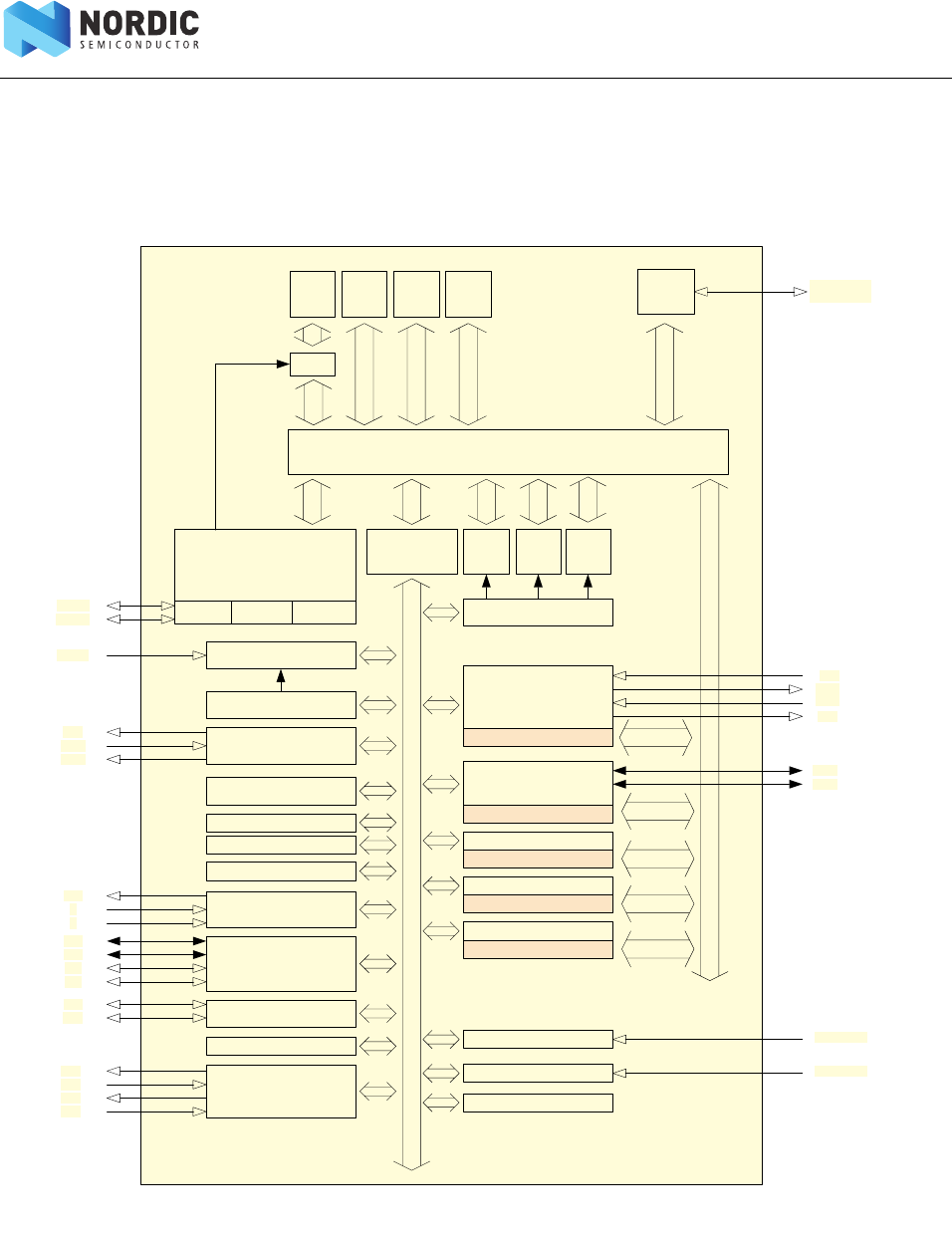
2.1 Block diagram
Figure 1 illustrates the overall system. Arrows with white heads indicate signals that share physical pins with
other signals.
Figure 1 Block diagram
Q5)
$+%72$3%
%5,'*(
5$',2
$+%/,7(0XOWL/D\HU
VODYH
$50
&257(;0
(&%
'$3
63,
51*
4'(&
7(03
:'7
190&
$'&
*3,27(
*3,2
PDVWHU
$17
$17
3
3±3
32:(5
6:',2
$,1±$,1
6:&/.
5(6(7
6&.
0,62
026,
/('
$
%
57&
33,
8$57
&/2&.
;/
;/
;&
;&
7:,
6&/
6'$
7,0(5
19,&
8,&5
VODYH
5$0
VODYH
),&5
VODYH
5$0
5$0
5$0
17%
6:'3
VODYH
VODYH
VODYH
63,6
6&.
026,
0,62
&61
&&0
&2'(
VODYH
(DV\'0$
/3&203
(DV\'0$
(DV\'0$
(DV\'0$ PDVWHU
PDVWHU
$,1±$,1
VODYH
PDVWHU
PDVWHU
5;'
7;'
&76
576
$$5
(DV\'0$ PDVWHU

Page 9 of 195
nRF51 Series Reference Manual v2.0 - System overview
2.2 System blocks
2.2.1 ARM® CortexTM-M0
A low power ARM® CortexTM-M0 32 bit CPU is embedded in all nRF51 series devices. The ARM® CortexTM-M0
has a 16 bit instruction set with 32 bit extensions (Thumb-2® technology) that delivers high density code
with a small memory footprint. By using a single-cycle 32 bit multiplier, a 3-stage pipeline, and a Nested
Vector Interrupt Controller (NVIC), the ARM® CortexTM-M0 CPU makes program execution simple and highly
efficient.
The ARM® Cortex Microcontroller Software Interface Standard (CMSIS) hardware abstraction layer for the
ARM® Cortex-M processor series is implemented and available for M0 CPU. Code is forward compatible with
ARM® Cortex-M3 based devices.
2.2.2 2.4 GHz radio
The nRF51 series ultra-low power 2.4 GHz GFSK RF transceiver is designed and optimized to operate in the
worldwide ISM frequency band at 2.400 GHz to 2.4835 GHz. Configurable radio modulation modes and
packet structure makes the transceiver interoperable with Bluetooth low energy (BLE), ANTTM, Gazell,
Enhanced ShockburstTM, and a range of other 2.4 GHz protocol implementations.
The transceiver receives and transmits data directly to and from system memory. It is stored in clear text
even when encryption is enabled, so packet data management is flexible and efficient.
2.2.3 Power management
The nRF51 series power management system is orthogonal and highly flexible with only simple ON or OFF
modes governing a whole device. In System OFF mode, everything is powered down but sections of the
RAM can be retained. The device state can be changed to System ON through reset or wake up from all
GPIOs. When in System ON mode, all functional blocks are accessible with each functional block remaining
in IDLE mode and only entering RUN mode when required.
2.2.4 PPI system
The Programmable Peripheral Interconnect (PPI) enables different peripherals to interact autonomously
with each other using tasks and events without use of the CPU. The PPI provides a mechanism to
automatically trigger a task in one peripheral as a result of an event occurring in another. A task is connected
to an event through a PPI channel.
2.2.5 Debugger support
The 2 pin Serial Wire Debug interface (provided as a part of the Debug Access Port, DAP) offers in
conjunction with the Basic Branch Buffer (BBB) a flexible and powerful mechanism for non-intrusive
program code debugging. This includes adding breakpoints in the code, performing single stepping, and
capturing instruction trace of parts of the code execution flow.

Page 10 of 195
nRF51 Series Reference Manual v2.0 - CPU
3 CPU
A low power ARM® CortexTM-M0 32 bit CPU is embedded in all nRF51 series devices. The ARM® CortexTM-M0
has a 16 bit instruction set with 32 bit extensions (Thumb-2® technology) that delivers high density code
with a small memory footprint. By using a single-cycle 32 bit multiplier, a 3-stage pipeline, and a Nested
Vector Interrupt Controller (NVIC), the ARM® CortexTM-M0 CPU makes program execution simple and highly
efficient.
The ARM® CortexTM Microcontroller Software Interface Standard (CMSIS) hardware abstraction layer for the
ARM® CortexTM-M processor series is implemented and available for M0 CPU. Code is forward compatible
with ARM® CortexTM-M3 based devices.
For further information on the embedded ARM® CortexTM-M0 CPU, please refer to www.arm.com/products/
processors/cortex-m/cortex-m0.php.

Page 11 of 195
nRF51 Series Reference Manual v2.0 - Memory
4 Memory
Figure 2 Memory map
4.1 Functional description
All memory blocks and registers in the nRF51 series are placed in a common memory map.
4.1.1 Memory categories
There are three main categories of memory:
• Code memory
• Random Access Memory (RAM)
• Peripheral registers (PER)
In addition, there is one information block (FICR) containing read only parameters describing configuration
details of the device and another information block (UICR) that can be configured by the user.
reserved
0xFFFFFFFF
Private Peripheral Bus
0xE0100000
reserved
AHB peripherals
0xE0000000
0x50000000
APB peripherals
reserved
RAM
0x40000000
0x20000000
reserved
FICR
reserved
reserved
Code
0x00000000
0x10000000
0x40080000
UICR
reserved
0x10001000

Page 12 of 195
nRF51 Series Reference Manual v2.0 - Memory
4.1.2 Memory types
The various memory categories can have one of the following memory types:
• Volatile memory (VM)
• Non-volatile memory (NVM)
Volatile memory is a type of memory that will lose its contents when the chip loses power. This memory
type can be read/written an unlimited number of times by the CPU.
Non-volatile memory is a type of memory that can retain stored information even when the chip loses
power. This memory type can be read an unlimited number of times by the CPU, but have restrictions on the
number of times it can be written and also on how it can be written. Writing to non-volatile memory is
managed by the Non Volatile Memory Controller (NVMC).
4.1.3 Code memory
The code memory is normally used for storing the program run by the CPU, but can also be used for storing
data constants that are retained when the chip loses power.
The code memory is non-volatile.
4.1.4 Random Access Memory (RAM)
RAM is normally used by the CPU program for temporary data storage, but it is also possible to run a CPU
program from RAM.
The RAM is divided into multiple RAM blocks that can be further divided into multiple RAM sections, that is,
a RAM block may contain one or more RAM sections. More information about how these RAM blocks are
divided can be found in the device specific product specifications.
The RAM is located from address 0x20000000 in the address space.
The RAM is volatile and always loses its contents when the chip loses power. The RAM may also lose its
contents when entering System OFF power saving mode. Whether the contents of a particular RAM block
are lost in System OFF power saving mode is dependent on the settings in the RAMON register in the
POWER peripheral.
4.1.5 Peripheral registers
The peripheral registers are registers used for interfacing to peripheral units such as timers, the radio, the
ADC, and so on.

Page 13 of 195
nRF51 Series Reference Manual v2.0 - Memory
4.2 Instantiation
The nRF51 series peripheral instantiation is shown in the table below.
Table 3 Peripheral instantiation
ID Base address Peripheral Instance Description
00x40000000 POWER POWER Power control
00x40000000 CLOCK CLOCK Clock control
10x40001000 RADIO RADIO 2.4 GHz Radio
20x40002000 UART UART0 Universal Asynchronous Receiver/Transmitter 0
30x40003000 SPI SPI0 Serial Peripheral Interface
30x40003000 TWI TWI0 I2C compatible Two-Wire Interface
40x40004000 SPI SPI1 Serial Peripheral Interface
40x40004000 TWI TWI1 I2C compatible Two-Wire Interface 1
40x40004000 SPIS SPIS1 SPI slave
60x40006000 GPIOTE GPIOTE GPIO Tasks and Events
70x40007000 ADC ADC Analog-to-Digital Converter
80x40008000 TIMER TIMER0 Timer/counter 0
90x40009000 TIMER TIMER1 Timer/counter 1
10 0x4000A000 TIMER TIMER2 Timer/counter 2
11 0x4000B000 RTC RTC0 Real Time Counter 0
12 0x4000C000 TEMP TEMP Temperature sensor
13 0x4000D000 RNG RNG Random number generator
14 0x4000E000 ECB ECB Crypto ECB
15 0x4000F000 CCM CCM AES CCM mode encryption
15 0x4000F000 AAR AAR Accelerated Address Resolver
16 0x40010000 WDT WDT Watchdog timer
17 0x40011000 RTC RTC1 Real Time Counter 1
18 0x40012000 QDEC QDEC Quadrature Decoder
19 0x40013000 LPCOMP LPCOMP Low power comparator
20
...
29
30 0x4001E000 NVMC NVMC Non-volatile memory controller
31 0x4001F000 PPI PPI Programmable Peripheral Interconnect
NA 0x50000000 GPIO P0 General purpose input and output
NA 0x10000000 FICR FICR Factory Information Configuration Registers
NA 0x10001000 UICR UICR User Information Configuration Registers

Page 14 of 195
nRF51 Series Reference Manual v2.0 - Non-Volatile Memory Controller (NVMC)
5 Non-Volatile Memory Controller (NVMC)
The Non-volatile Memory Controller (NVMC) is used for writing and erasing Non-volatile Memory (NVM).
Before a write can be performed the NVM must be enabled for writing in CONFIG.WEN. Similarly, before an
erase can be performed the NVM must be enabled for erasing in CONFIG.EEN. The user must make sure that
writing and erasing is not enabled at the same time, failing to do so may result in unpredictable behavior.
5.1 Functional description
5.1.1 Writing to the NVM
When writing is enabled, the NVM is written by writing a word to a word aligned address in the CODE or
UICR. The NVMC is only able to write bits in the NVM that are erased, that is, set to '1'.
The time it takes to write a word to the NVM is specified by tWRITE in the product specification. The CPU is
halted while the NVMC is writing to the NVM.
Only word aligned writes are allowed. Byte or half word aligned writes will result in a hard fault.
5.1.2 Writing to User Information Configuration Registers
UICR registers are written as ordinary non-volatile memory. After the UICR has been written, the new UICR
configuration will only take effect after a reset.
5.1.3 Erasing User Information Configuration Registers
There are two registers that can be used for erasing the UICR, the ERASEALL and the ERASEUICR. When
readback protection is configured, writing the ERASEUICR register only has an effect when the entire region
1 of code memory is erased (all ‘1’s).
The time it takes to perform an ERASEUICR command is specified by tPAGEERASE in the product specification.
The CPU is halted while the NVMC performs the erase operation.
5.1.4 Erase all
When erase is enabled, the whole CODE and UICR can be erased in one operation by using the ERASEALL
register. ERASEALL will not erase the Factory Information Configuration Registers (FICR).
The time it takes to perform an ERASEALL operation is specified by tERASEALL in the product specification.
The CPU is halted while the NVMC performs the erase operation.
5.1.5 Erasing a page in code region 1
When erase is enabled, the NVM can be erased page by page using the ERASEPAGE register or the
ERASEPCR1 register. After erasing a NVM page all bits in the page are set to ‘1’. The time it takes to erase a
page is specified by tPAGEERASE in the product specification. The CPU is halted while the NVMC performs the
erase operation.

Page 15 of 195
nRF51 Series Reference Manual v2.0 - Non-Volatile Memory Controller (NVMC)
5.1.6 Erasing a page in code region 0
ERASEPCR0 is used to erase a page in code region 0. The ERASEPCR0 register can only be accessed from a
program running in code region 0.
To enable non-volatile storage for program running in code region 0, it is possible for this program to erase
and re-write any code page it designates for this purpose within code region 0. The ERASEPCR0 can be used
for this purpose. The ERASEPCR0 register has a restriction on its use, enforced by the MPU, where only code
running from code region 0 can write to it. It is possible for a program running from code region 0 to erase a
page in code region 1 using ERASEPCR1.
The time it takes to erase a page is specified by tPAGEERASE in the product specification.
5.1.7 Availability of erase operations based on presence of pre-programmed factory
code
To enable independent readback protection of code region 0 and code region 1, and to ensure that a
developer cannot erase factory-programmed code from region 0, the ERASEALL and ERASEUICR registers
are not always available. The following table shows when the registers can and cannot be used. When a
register is disabled, attempting to write it will have no effect.
Table 4 Available erase operations dependent on presence of pre-programmed factory code
5.2 Registers
Table 5 Register overview
FICR.PPFC1
1. See Chapter 6 “Factory Information Configuration Regis-
ters (FICR)” on page 18 for details.
Available
operations
Unavailable
registers
0XFF
(Pre-programmed
code not present)
ERASEALL ERASEUICR
0x00
(Pre-programmed
code present)
ERASEUICR ERASEALL
Register Offset Description
REGISTERS
READY 0x400 Ready flag
CONFIG 0x504 Configuration register
ERASEPAGE 0x508 Register for erasing a page in code region 1
ERASEPCR1 0x508 Register for erasing a page in code region 1. Equivalent to ERASEPAGE.
ERASEPCR0 0x510 Register for erasing a page in code region 0
ERASEALL 0x50C Register for erasing all non-volatile user memory
ERASEUICR 0x514 Register for erasing User Information Configuration Registers

Page 16 of 195
nRF51 Series Reference Manual v2.0 - Non-Volatile Memory Controller (NVMC)
5.2.1 READY
5.2.2 CONFIG
5.2.3 ERASEALL
5.2.4 ERASEUICR
Bit number 31 30 29 28 27 26 25 24 23 22 21 20 19 18 17 16 15 14 13 12 11 10 9 8 7 6 5 4 3 2 1 0
ID (Field ID) - - - - - - - - - - - - - - - - - - - - - - - - - - - - - - - A
Reset value 0 0 0 0 0 0 0 0 0 0 0 0 0 0 0 0 0 0 0 0 0 0 0 0 0 0 0 0 0 0 0 0
ID RW Field Value ID Value Description
AR
0NVMC is busy (on-going write or erase operation).
1NVMC is ready.
Bit number 31 30 29 28 27 26 25 24 23 22 21 20 19 18 17 16 15 14 13 12 11 10 9 8 7 6 5 4 3 2 1 0
ID (Field ID) ------------------------------AA
Reset value 00000000000000000000000000000000
ID RW Field Value ID Value Description
A RW WEN Program memory access mode. It is strongly recommended to only activate
erase and write modes when they are actively used.
REN 0Read only access.
WEN 1 Write Enabled.
EEN 2Erase enabled.
Bit number 31 30 29 28 27 26 25 24 23 22 21 20 19 18 17 16 15 14 13 12 11 10 9 8 7 6 5 4 3 2 1 0
ID (Field ID) - - - - - - - - - - - - - - - - - - - - - - - - - - - - - - - A
Reset value 0 0 0 0 0 0 0 0 0 0 0 0 0 0 0 0 0 0 0 0 0 0 0 0 0 0 0 0 0 0 0 0
ID RW Field Value ID Value Description
A RW Erase all non-volatile memory including UICR registers. Code erase has to be
enabled by CONFIG.EEN before the non-volatile memory can be erased.
Note: FICR is not erased.
0No operation.
1Start chip erase.
Bit number 31 30 29 28 27 26 25 24 23 22 21 20 19 18 17 16 15 14 13 12 11 10 9 8 7 6 5 4 3 2 1 0
ID (Field ID) - - - - - - - - - - - - - - - - - - - - - - - - - - - - - - - A
Reset value 0 0 0 0 0 0 0 0 0 0 0 0 0 0 0 0 0 0 0 0 0 0 0 0 0 0 0 0 0 0 0 0
ID RW Field Value ID Value Description
A RW Register starting erase of all User Information Configuration Registers. Note that
code erase has to be enabled by CONFIG.EEN before the UICR can be erased.
0No operation.
1 Start erase of UICR.

Page 17 of 195
nRF51 Series Reference Manual v2.0 - Non-Volatile Memory Controller (NVMC)
5.2.5 ERASEPAGE/ERASEPCR1
5.2.6 ERASEPCR0
Bit number 31 30 29 28 27 26 25 24 23 22 21 20 19 18 17 16 15 14 13 12 11 10 9 8 7 6 5 4 3 2 1 0
ID (Field ID) A A A A A A A A A A A A A A A A A A A A A A A A A A A A A A A A
Reset value 0 0 0 0 0 0 0 0 0 0 0 0 0 0 0 0 0 0 0 0 0 0 0 0 0 0 0 0 0 0 0 0
ID RW Field Value ID Value Description
A RW Register for starting erase of a page in code region 1.
The value is the address of the page to be erased (addresses of first word in page).
Note that code erase must be enabled by CONFIG.EEN before any pages in code
region 1 can be erased.
See product specification for information about the total code size of the device
you are using. Attempts to erase pages that are outside the code area may result
in undesirable behavior, for example, the wrong page may be erased.
Bit number 31 30 29 28 27 26 25 24 23 22 21 20 19 18 17 16 15 14 13 12 11 10 9 8 7 6 5 4 3 2 1 0
ID (Field ID) A A A A A A A A A A A A A A A A A A A A A A A A A A A A A A A A
Reset value 0 0 0 0 0 0 0 0 0 0 0 0 0 0 0 0 0 0 0 0 0 0 0 0 0 0 0 0 0 0 0 0
ID RW Field Value ID Value Description
A RW Register for starting erase of a page in code region 0.
The value is the address of the page to be erased (addresses of first word in page).
Only page addresses in code region 0 are allowed. This register can only be
accessed from a program running in code memory region 0. A hard fault will be
generated if the register is attempted accessed from a program in RAM or code
memory region 1.
Writing to ERASEPRC0 from the Serial Wire Debug (SWD) will have no effect.
CONFIG.EEN has to be set to enable erase.
See product specification for information about the total code size of the device
you are using. Attempts to erase pages that are outside the code area may result
in undesirable behavior, for example, the wrong page may be erased.

Page 18 of 195
nRF51 Series Reference Manual v2.0 - Factory Information Configuration Registers (FICR)
6 Factory Information Configuration Registers (FICR)
6.1 Functional description
Factory Information Configuration Registers are pre-programmed in factory and cannot be erased by the
user. These registers contain chip specific information and configuration.
6.1.1 Override parameters
Factory Information Configuration Registers contain override parameters set during device calibration in
production, which need to replace default settings in the RADIO. Override parameters and the RADIO mode
they are used for varies between nRF51 devices. Read the OVERRIDDEN register to determine if the FICR
contains override parameters for the radio mode you are going to use. If the FICR contains override
parameters, they must be copied to the radio OVERRIDE registers before enabling the radio in that mode.

Page 19 of 195
nRF51 Series Reference Manual v2.0 - Factory Information Configuration Registers (FICR)
6.2 Registers
Table 6 Register overview
Register Offset Description
CODEPAGESIZE 0x010 Code memory page size
CODESIZE 0x014 Code memory size
CLENR0 0x028 Length of code region 0 in bytes
PPFC 0x02C Pre-programmed factory code present
NUMRAMBLOCK 0x034 Number of individually controllable RAM blocks
SIZERAMBLOCK[0] 0x038 Size of RAM block 0 in bytes
SIZERAMBLOCK[1] 0x03C Size of RAM block 1 in bytes
SIZERAMBLOCK[2] 0x040 Size of RAM block 2 in bytes
SIZERAMBLOCK[3] 0x044 Size of RAM block 3 in bytes
CONFIGID 0x05C Configuration identifier
DEVICEID[0] 0x060 Device identifier, bit 31-0
DEVICEID[1] 0x064 Device identifier, bit 63-32
ER[0] 0x080 Encryption root, bit 31-0
ER[1] 0x084 Encryption root, bit 63-32
ER[2] 0x088 Encryption root, bit 95-64
ER[3] 0x08C Encryption root, bit 127-96
IR[0] 0x090 Identity root, bit 31-0
IR[1] 0x094 Identity root, bit 63-32
IR[2] 0x098 Identity root, bit 95-64
IR[3] 0x09c Identity root, bit 127-96
DEVICEADDRTYPE 0x0A0 Device address type
DEVICEADDR[0] 0x0A4 Device address, bit 31-0
DEVICEADDR[1] 0x0A8 Device address, bit 47-32
OVERRIDDEN 0x0AC Override enable
BLE_1MBIT[0] 0x0EC RADIO.OVERRIDE[0] values for BLE_1MBIT mode
BLE_1MBIT[1] 0x0F0 RADIO.OVERRIDE[1] values for BLE_1MBIT mode
BLE_1MBIT[2] 0x0F4 RADIO.OVERRIDE[2] values for BLE_1MBIT mode
BLE_1MBIT[3] 0x0F8 RADIO.OVERRIDE[3] values for BLE_1MBIT mode
BLE_1MBIT[4] 0x0FC RADIO.OVERRIDE[4] values for BLE_1MBIT mode

Page 20 of 195
nRF51 Series Reference Manual v2.0 - Factory Information Configuration Registers (FICR)
6.2.1 CODEPAGESIZE
6.2.2 CODESIZE
6.2.3 CLENR0
6.2.4 PPFC
Bit number 31 30 29 28 27 26 25 24 23 22 21 20 19 18 17 16 15 14 13 12 11 10 9 8 7 6 5 4 3 2 1 0
ID (Field ID) A A A A A A A A A A A A A A A A A A A A A A A A A A A A A A A A
Value after erase 1 1 1 1 1 1 1 1 1 1 1 1 1 1 1 1 1 1 1 1 1 1 1 1 1 1 1 1 1 1 1 1
ID RW Field Value ID Value Description
A R Code memory page size in bytes
Bit number 31 30 29 28 27 26 25 24 23 22 21 20 19 18 17 16 15 14 13 12 11 10 9 8 7 6 5 4 3 2 1 0
ID (Field ID) AAAAAAAAAAAAAAAAAAAAAAAAAAAAAAAA
Value after erase 11111111111111111111111111111111
ID RW Field Value ID Value Description
A R Code memory size in number of pages. Total code space is:
CODEPAGESIZE*CODESIZE
Bit number 31 30 29 28 27 26 25 24 23 22 21 20 19 18 17 16 15 14 13 12 11 10 9 8 7 6 5 4 3 2 1 0
ID (Field ID) A A A A A A A A A A A A A A A A A A A A A A A A A A A A A A A A
Value after erase 1 1 1 1 1 1 1 1 1 1 1 1 1 1 1 1 1 1 1 1 1 1 1 1 1 1 1 1 1 1 1 1
ID RW Field Value ID Value Description
AR [0..N]
0xFFFFFFFF
Length of code region 0 in bytes. The value must be multiple of “code page size”
bytes (FICR.CODEPAGESIZE). This register is only used when pre-programmed
factory code is present on the chip, see PPFC.
N (max value) is (FICR.CODEPAGESIZE* FICR.CODESIZE-1, but not larger than 255.
This register can only be written if content is 0xFFFFFFFF.
Value if there is no pre-programmed code in the chip. Interpreted as 0.
Bit number 31 30 29 28 27 26 25 24 23 22 21 20 19 18 17 16 15 14 13 12 11 10 9 8 7 6 5 4 3 2 1 0
ID (Field ID) - - - - - - - - - - - - - - - - - - - - - - - - A A A A A A A A
Value after erase 1 1 1 1 1 1 1 1 1 1 1 1 1 1 1 1 1 1 1 1 1 1 1 1 1 1 1 1 1 1 1 1
ID RW Field Value ID Value Description
AR ADDR
0x00
0xFF
Pre-programmed factory code present.
Present
Not present

Page 21 of 195
nRF51 Series Reference Manual v2.0 - Factory Information Configuration Registers (FICR)
6.2.5 NUMRAMBLOCK
6.2.6 SIZERAMBLOCK[n] (n=0..3)
6.2.7 CONFIGID
6.2.8 DEVICEID[0]
6.2.9 DEVICEID[1]
Bit number 31 30 29 28 27 26 25 24 23 22 21 20 19 18 17 16 15 14 13 12 11 10 9 8 7 6 5 4 3 2 1 0
ID (Field ID) AAAAAAAAAAAAAAAAAAAAAAAAAAAAAAAA
Value after erase 11111111111111111111111111111111
ID RW Field Value ID Value Description
A R Number of individually controllable RAM blocks.
Bit number 31 30 29 28 27 26 25 24 23 22 21 20 19 18 17 16 15 14 13 12 11 10 9 8 7 6 5 4 3 2 1 0
ID (Field ID) AAAAAAAAAAAAAAAAAAAAAAAAAAAAAAAA
Value after erase 11111111111111111111111111111111
ID RW Field Value ID Value Description
A R Size of RAM block n in bytes.
Bit number 31 30 29 28 27 26 25 24 23 22 21 20 19 18 17 16 15 14 13 12 11 10 9 8 7 6 5 4 3 2 1 0
ID (Field ID) B B B B B B B B B B B B B B B B A A A A A A A A A A A A A A A A
Value after erase 1 1 1 1 1 1 1 1 1 1 1 1 1 1 1 1 1 1 1 1 1 1 1 1 1 1 1 1 1 1 1 1
ID RW Field Value ID Value Description
A R HWID Identification number for the HW.
B R FWID Identification number for the firmware that is pre-loaded into the chip.
Bit number 31 30 29 28 27 26 25 24 23 22 21 20 19 18 17 16 15 14 13 12 11 10 9 8 7 6 5 4 3 2 1 0
ID (Field ID) A A A A A A A A A A A A A A A A A A A A A A A A A A A A A A A A
Value after erase 1 1 1 1 1 1 1 1 1 1 1 1 1 1 1 1 1 1 1 1 1 1 1 1 1 1 1 1 1 1 1 1
ID RW Field Value ID Value Description
A R Device ID, bit 31-0, unique ID for each unit.
Bit number 31 30 29 28 27 26 25 24 23 22 21 20 19 18 17 16 15 14 13 12 11 10 9 8 7 6 5 4 3 2 1 0
ID (Field ID) A A A A A A A A A A A A A A A A A A A A A A A A A A A A A A A A
Value after erase 1 1 1 1 1 1 1 1 1 1 1 1 1 1 1 1 1 1 1 1 1 1 1 1 1 1 1 1 1 1 1 1
ID RW Field Value ID Value Description
A R Device ID, bit 63-32, unique ID for each unit.

Page 22 of 195
nRF51 Series Reference Manual v2.0 - Factory Information Configuration Registers (FICR)
6.2.10 ER[n] (n=0..3)
6.2.11 IR[n] (n=0..3)
6.2.12 DEVICEADDRTYPE
6.2.13 DEVICEADDR[0]
6.2.14 DEVICEADDR[1]
Bit number 31 30 29 28 27 26 25 24 23 22 21 20 19 18 17 16 15 14 13 12 11 10 9 8 7 6 5 4 3 2 1 0
ID (Field ID) A A A A A A A A A A A A A A A A A A A A A A A A A A A A A A A A
Value after erase 1 1 1 1 1 1 1 1 1 1 1 1 1 1 1 1 1 1 1 1 1 1 1 1 1 1 1 1 1 1 1 1
ID RW Field Value ID Value Description
A R Encryption root, word n.
Bit number 31 30 29 28 27 26 25 24 23 22 21 20 19 18 17 16 15 14 13 12 11 10 9 8 7 6 5 4 3 2 1 0
ID (Field ID) A A A A A A A A A A A A A A A A A A A A A A A A A A A A A A A A
Value after erase 1 1 1 1 1 1 1 1 1 1 1 1 1 1 1 1 1 1 1 1 1 1 1 1 1 1 1 1 1 1 1 1
ID RW Field Value ID Value Description
A R Identity root, word n.
Bit number 31 30 29 28 27 26 25 24 23 22 21 20 19 18 17 16 15 14 13 12 11 10 9 8 7 6 5 4 3 2 1 0
ID (Field ID) - - - - - - - - - - - - - - - - - - - - - - - - - - - - - - - A
Value after erase 1 1 1 1 1 1 1 1 1 1 1 1 1 1 1 1 1 1 1 1 1 1 1 1 1 1 1 1 1 1 1 1
ID RW Field Value ID Value Description
AR
PUBLIC
RANDOM
0
1
Device address type
Public address
Random address
Bit number 31 30 29 28 27 26 25 24 23 22 21 20 19 18 17 16 15 14 13 12 11 10 9 8 7 6 5 4 3 2 1 0
ID (Field ID) A A A A A A A A A A A A A A A A A A A A A A A A A A A A A A A A
Value after erase 1 1 1 1 1 1 1 1 1 1 1 1 1 1 1 1 1 1 1 1 1 1 1 1 1 1 1 1 1 1 1 1
ID RW Field Value ID Value Description
A R ADDR Device address bit 31-0.
Bit number 31 30 29 28 27 26 25 24 23 22 21 20 19 18 17 16 15 14 13 12 11 10 9 8 7 6 5 4 3 2 1 0
ID (Field ID) - - - - - - - - - - - - - - - - A A A A A A A A A A A A A A A A
Value after erase 1 1 1 1 1 1 1 1 1 1 1 1 1 1 1 1 1 1 1 1 1 1 1 1 1 1 1 1 1 1 1 1
ID RW Field Value ID Value Description
A R ADDR Device address bit 47-32.

Page 23 of 195
nRF51 Series Reference Manual v2.0 - Factory Information Configuration Registers (FICR)
6.2.15 OVERRIDDEN
6.2.16 NRF_1MBIT[n] (n=0..4)
6.2.17 BLE_1MBIT[n] (n=0..4)
Bit number 31 30 29 28 27 26 25 24 23 22 21 20 19 18 17 16 15 14 13 12 11 10 9 8 7 6 5 4 3 2 1 0
ID (Field ID) - - - - - - - - - - - - - - - - - - - - - - - - - - - - D - - A
Value after erase - - - - - - - - - - - - - - - - - - - - - - - - - - - - - - - -
ID RW Field Value ID Value Description
AR NRF_1MBIT 0
1
Override default values for NRF_1MBIT mode.
Use default values for NRF_1MBIT mode.
D R BLE_1MBIT 0
1
Override values for BLE_1MBIT mode is available in FICR.BLE_1MBIT[n] (n=0..4).
No override values for BLE_1MBIT mode available in FICR.
Bit number 31 30 29 28 27 26 25 24 23 22 21 20 19 18 17 16 15 14 13 12 11 10 9 8 7 6 5 4 3 2 1 0
ID (Field ID) A A A A A A A A A A A A A A A A A A A A A A A A A A A A A A A A
Value after erase - - - - - - - - - - - - - - - - - - - - - - - - - - - - - - - -
ID RW Field Value ID Value Description
A R Override values for NRF_1MBIT mode.
Bit number 31 30 29 28 27 26 25 24 23 22 21 20 19 18 17 16 15 14 13 12 11 10 9 8 7 6 5 4 3 2 1 0
ID (Field ID) A A A A A A A A A A A A A A A A A A A A A A A A A A A A A A A A
Value after erase - - - - - - - - - - - - - - - - - - - - - - - - - - - - - - - -
ID RW Field Value ID Value Description
A R Override values for BLE_1MBIT mode.

Page 24 of 195
nRF51 Series Reference Manual v2.0 - User Information Configuration Registers (UICR)
7 User Information Configuration Registers (UICR)
7.1 Functional description
The User Information Configuration Registers (UICRs) are NVM registers for configuring user specific settings
including code readback protection of the whole code area, or a part of the code area.
The code area can be divided into two regions, code region 0 (CR0) and code region 1 (CR1). Code region 0
starts at address 0x00000000 and stretches into the code area as specified in the CLENR0 register. The area
above CLENR0 will then be defined as code region 1. If CLENR0 is not configured, that is, has the value
0xFFFFFFFF, the whole code area will be defined as code region 1 (CR1).
Code running from code region 1 will not be able to write to code region 0. Additionally, the content of code
region 0 cannot be read from code running in code region 1 or through the SWD interface if code region 0 is
readback protected, see Section 7.2.2 “RBPCONF” on page 25.
The main readback protection mechanism that will protect the whole code, that is, both code region 0 and
code region 1, is also configured through the UICR, see Section 7.2.2 “RBPCONF” on page 25.
The PAGEERASE command in NVMC will only work for code region 1. See Chapter 5 “Non-Volatile Memory
Controller (NVMC)” on page 14 for more information on how to erase and program the code area and the
UICR.
7.2 Registers
Table 7 Register overview
7.2.1 CLENR0
Register Offset Description
REGISTERS
CLENR0 0x000 Length of code region 0.
RBPCONF 0x004 Read back protection configuration.
XTALFREQ 0x008 Reset value for XTALFREQ in clock, see Chapter 12 “Clock
management (CLOCK)” on page 53.
FWID 0x010
0x014 - 0x02C
0x030 - 0x07C
0x080 - 0x0FC
Firmware ID.
Reserved.
Reserved.
Reserved for customer.
Bit number 31 30 29 28 27 26 25 24 23 22 21 20 19 18 17 16 15 14 13 12 11 10 9 8 7 6 5 4 3 2 1 0
ID (Field ID) A A A A A A A A A A A A A A A A A A A A A A A A A A A A A A A A
Value after erase 1 1 1 1 1 1 1 1 1 1 1 1 1 1 1 1 1 1 1 1 1 1 1 1 1 1 1 1 1 1 1 1
ID RW Field Value ID Value Description
A RW [0..N] Length of code region 0 in bytes. The value must be a multiple of “code page size”
bytes (FICR. CODEPAGESIZE).
N (max value) is (FICR.CODEPAGESIZE* FICR.CODESIZE-1), but not larger than 255.
This register can only be written if content is 0xFFFFFFFF.
This register is only used when pre-programmed factory code is not present on the
chip, see PPFC in FICR.

Page 25 of 195
nRF51 Series Reference Manual v2.0 - User Information Configuration Registers (UICR)
7.2.2 RBPCONF
7.2.3 XTALFREQ
7.2.4 FWID
0xFFFFFFFF Value after mass erase of flash. Interpreted as 0.
Bit number 31 30 29 28 27 26 25 24 23 22 21 20 19 18 17 16 15 14 13 12 11 10 9 8 7 6 5 4 3 2 1 0
ID (Field ID) - - - - - - - - - - - - - - - - B B B B B B B B A A A A A A A A
Value after erase 1 1 1 1 1 1 1 1 1 1 1 1 1 1 1 1 1 1 1 1 1 1 1 1 1 1 1 1 1 1 1 1
ID RW Field Value ID Value Description
ARWPR0
0xFF
0x00
Readback protect code region 0. Will be ignored if preprogrammed factory code
is present on the chip.
Disabled
Enabled
BRW PALL
0xFF
0x00
Readback protect all code in device.
Disabled
Enabled
Bit number 31 30 29 28 27 26 25 24 23 22 21 20 19 18 17 16 15 14 13 12 11 10 9 8 7 6 5 4 3 2 1 0
ID (Field ID) - - - - - - - - - - - - - - - - - - - - - - - - A A A A A A A A
Value after erase 1 1 1 1 1 1 1 1 1 1 1 1 1 1 1 1 1 1 1 1 1 1 1 1 1 1 1 1 1 1 1 1
ID RW Field Value ID Value Description
AR
0xFF
0x00
Reset value for XTALFREQ in CLOCK, see Chapter 12 “Clock management
(CLOCK)” on page 53.
16 MHz crystal is used.
32 MHz crystal is used.
Bit number 31 30 29 28 27 26 25 24 23 22 21 20 19 18 17 16 15 14 13 12 11 10 9 8 7 6 5 4 3 2 1 0
ID (Field ID) - - - - - - - - - - - - - - - - A A A A A A A A A A A A A A A A
Value after erase 1 1 1 1 1 1 1 1 1 1 1 1 1 1 1 1 1 1 1 1 1 1 1 1 1 1 1 1 1 1 1 1
ID RW Field Value ID Value Description
A R Identification number for the firmware loaded into the chip. This ID is used when
the CONFIG.FWID in the FICR is set to 0xFFFF
Bit number 31 30 29 28 27 26 25 24 23 22 21 20 19 18 17 16 15 14 13 12 11 10 9 8 7 6 5 4 3 2 1 0
ID (Field ID) A A A A A A A A A A A A A A A A A A A A A A A A A A A A A A A A
Value after erase 1 1 1 1 1 1 1 1 1 1 1 1 1 1 1 1 1 1 1 1 1 1 1 1 1 1 1 1 1 1 1 1
ID RW Field Value ID Value Description
Page 26 of 195
nRF51 Series Reference Manual v2.0 - Memory Protection Unit (MPU)
8 Memory Protection Unit (MPU)
The Memory Protection Unit (MPU) can protect the entire memory against readback and also protect parts
of the memory area from accidental access by the CPU.
Figure 3 MPU block diagram
8.1 Functional description
Protect all (PALL) is configured by writing '0' to UICR.RBPCONF.PALL. When enabled, the debugger (SWD) will
no longer have access to code region 0 or code region 1, as well as no longer being able to access RAM or
any peripherals except for the NVMC. The debugger will always have access to the NVMC peripheral
independent of protection settings.
Code memory, RAM, and peripherals can be divided into two regions: region 0 and region 1. Code memory
regions are configured in the CLENR0 register in the User Information Configuration Register (UICR), see the
Memory isolation and run-time protection section in the Appendix A: on page 186. When memory
protection is enabled, these regions will be used by the Memory Protection Unit to enforce runtime
protection and readback protection of resources classified as region 0.
Independent of protection settings, code region R0 (CR0) will always have full access to the system. The
NVMC.ERASEPCR0 register, which is used to erase contents from code region 0, can only be accessed from a
program in code region 0.
Only the CPU can do fetches from code memory, and these will always be granted.
Except when generated by the SWD interface, accesses that are not granted by the MPU will result in a hard-
fault.
Readback protection of code region 0 is enabled by writing '0' to UICR.RBPCONF.PR0. When enabled, only
code running from code region 0 will be able to access the code in code region 0. Accesses generated by
code running from code region 1 or from RAM, as well as accesses generated by the debugger (SWD), will
not be granted when code region 0 is protected.
The main role for the two region memory protection system is to allow run time protection for SoftDevices
installed running on the IC. Please refer to Appendix A: on page 186 for a description of the nRF51 software
architecture and use of the memory protection system with SoftDevices.
MPU
Configuration
Requester
information
Request target
information
Decision
(FA, LA,
NA0 or NA1)

Page 27 of 195
nRF51 Series Reference Manual v2.0 - Memory Protection Unit (MPU)
8.1.1 Inputs
The MPU has three classes of inputs. These are:
• Configuration
• Readback protection configuration from UICR and FICR.
• Information about requester
• Source of memory access request (SWD or CPU program).
• If the request source is a CPU program; region from which the program is running
(region 0 or region 1).
• Type of access request (read or write).
• Target information
• Memory category requested access to (code, RAM, or PER).
• Memory region requested access to (region 0 or region 1).
8.1.2 Output
The MPU outputs the level of memory access that shall be given to a memory access request. The access
levels the MPU can give are as follows:
•Full Access (FA)
• Full read write access to the requested memory.
• Limited Access (LA)
• Full read access
• No write access. Write will generate hard fault exception.
• No Access 0 (NA0)
• No read or write access
•Read will return 0
• Write will have no effect
• No Access 1 (NA1)
• No read or write access
• Read or write will generate hard fault exception
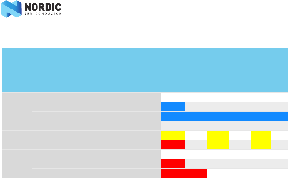
8.1.3 Output decision table
The output MPU access level based on the MPU inputs is given in the table below.
The given access level is dependent on settings in the Information Configuration Registers (ICRs). See the
UICR and FICR chapters for more details.
Page 28 of 195
nRF51 Series Reference Manual v2.0 - Memory Protection Unit (MPU)
X: Don’t care
LA: Limited Access
NA0: No Access 0
NA1: No Access 1
FA: Full Access
Table 8 MPU output decision table based on the MPU inputs and the ICR configuration
8.1.4 Exceptions from table
There are some exceptions from Table 8. These exceptions are:
• The NVMC.ERASEALL and NVMC.ERASEUICR registers have conditional write access
depending on the readback protection settings in the Information Configuration registers.
These exceptions are described in the NVMC chapter, see Chapter 5 “Non-Volatile Memory
Controller (NVMC)” on page 14.
• The NVMC.ERASEPCR0 register can only be accessed from a program in code region 0.
• The UICR.CLENR0 and the FICR. CLENR0 registers can only be modified when the register
value equals the default value (0xFF). This is to avoid that the memory region limits are
modified to bypass readback protection.
8.1.5 NVM protection blocks
The protection mechanism for NVM can be used to prevent erroneous application code from erasing or
writing to protected blocks. Non-volatile memory can be protected from erases/writes depending on
settings in the PROTENSET registers. One bit in a PROTENSET register represents one protected block. There
are two PROTENSET registers of 32 bits which means there are 64 protectable blocks in total. See the device
specific product specifications for more information on how the NVM protection blocks are organized.
Request target
Request
source
UICR.RBPCONF.PALL
(Readback protect
entire code memory)
UICR.RBPCONF.PR0 or
FICR.PPFC*
(Readback protect code
region 0)
Code R0 Code
R1
RAM
R0
RAM
R1
PER
R0
PER
R1
SWD 0xFF 0xFF FA FA FA FA FA FA
0xFF 0x00 NA0 FA FA FA FA FA
0x00 XNA0 NA0 NA0 NA0 NA0 NA0
Code R0 X X FA FA FA FA FA FA
Code R1 X0xFF LA FA LA FA LA FA
X0x00 NA1 FA LA FA LA FA
RAM
R0 / R1
0xFF 0xFF FA FA FA FA FA FA
0xFF 0x00 NA1 FA FA FA FA FA
0x00 XNA1 NA1FAFAFAFA
Page 29 of 195
nRF51 Series Reference Manual v2.0 - Memory Protection Unit (MPU)
Note: If an erase or write to a protected block is detected, the CPU will hard fault. If an ERASEALL
operation is attempted from the CPU while any block is protected it will be blocked and the
CPU will hard fault.
On reset, all the protection bits are cleared. To ensure safe operation, the first task after reset must be to set
the protection bits. The only way of clearing protection bits is by resetting the device from any reset source.
The protection mechanism is turned off when in debug mode (a debugger is connected) and the
DISABLEINDEBUG register is set to disable.
Figure 4 Protected regions of program memory
8.2 Registers
Table 9 Register overview
Register Offset Description
PERR0 0x528 Definition of peripherals in memory region 0.
RLENR0 0x52C Length of RAM region 0.
PROTENSET0 0x600 Protection bit enable set register
PROTENSET1 0x604 Protection bit enable set register
DISABLEINDEBUG 0x608 Disable protection mechanism in debug mode
0
31 PROTENSET[0]
63
61
62
2
0
1
...
Program Memory
0x0
0
31 PROTENSET[1]

Page 30 of 195
nRF51 Series Reference Manual v2.0 - Memory Protection Unit (MPU)
8.2.1 PERR0
Bit number 31 30 29 28 27 26 25 24 23 22 21 20 19 18 17 16 15 14 13 12 11 10 9 8 7 6 5 4 3 2 1 0
ID (Field ID) Z Y - - - - - - - - - - T S R Q P O N M L K J I H G - E D C B A
Reset value 0000000000 0000000000000000000000
ID RW Field Value ID Value Description
ARWPOWER_CLOCK
REGION0
REGION1
0
1
Classify POWER and CLOCK and all other peripherals with ID=0, as region 0 or region 1
peripheral.
Region 0
Region 1
BRW RADIO
REGION0
REGION1
0
1
Classify RADIO as region 0 or region 1 peripheral.
Region 0
Region 1
CRWUART0
REGION0
REGION1
0
1
Classify UART0 as region 0 or region 1 peripheral.
Region 0
Region 1
DRW SPI0_TWI0
REGION0
REGION1
0
1
Classify SPI0 and TWI0 as region 0 or region 1 peripheral.
ERWSPI1_TWI1
REGION0
REGION1
0
1
Classify SPI1, SPIS1, and TWI1 as region 0 or region 1 peripheral.
Region 0
Region 1
GRW GPIOTE
REGION0
REGION1
0
1
Classify GPIOTE as region 0 or region 1 peripheral.
HRWADC
REGION0
REGION1
0
1
Classify ADC as region 0 or region 1 peripheral.
Region 0
Region 1
IRW TIMER0
REGION0
REGION1
0
1
Classify TIMER0 as region 0 or region 1 peripheral.
Region 0
Region 1
JRWTIMER1
REGION0
REGION1
0
1
Classify TIMER1 as region 0 or region 1 peripheral.
Region 0
Region 1
KRW TIMER2
REGION0
REGION1
0
1
Classify TIMER2 as region 0 or region 1 peripheral.
LRWRTC0
REGION0
REGION1
0
1
Classify RTC0 as region 0 or region 1 peripheral.
MRW TEMP
REGION0
REGION1
0
1
Classify TEMP as region 0 or region 1 peripheral.
NRWRNG
REGION0
REGION1
0
1
Classify RNG as region 0 or region 1 peripheral.
ORW ECB
REGION0
REGION1
0
1
Classify ECB as region 0 or region 1 peripheral.
PRWCCM_AAR
REGION0
REGION1
0
1
Classify CCM and AAR as region 0 or region 1 peripheral.
QRW WDT
REGION0
REGION1
0
1
Classify WDT as region 0 or region 1 peripheral.

Page 31 of 195
nRF51 Series Reference Manual v2.0 - Memory Protection Unit (MPU)
8.2.2 RLENR0
RRWRTC1
REGION0
REGION1
0
1
Classify RTC1 as region 0 or region 1 peripheral.
SRW QDEC
REGION0
REGION1
0
1
Classify QDEC as region 0 or region 1 peripheral.
TRWCOMP_LPCOMP
REGION0
REGION1
0
1
Classify COMP_LPCOMP as region 0 or region 1 peripheral.
YRW NVMC
REGION0
REGION1
0
1
Classify NVMC as region 0 or region 1 peripheral.
ZRWPPI
REGION0
REGION1
0
1
Classify PPI as region 0 or region 1 peripheral.
Bit number 31 30 29 28 27 26 25 24 23 22 21 20 19 18 17 16 15 14 13 12 11 10 9 8 7 6 5 4 3 2 1 0
ID (Field ID) A A A A A A A A A A A A A A A A A A A A A A A A A A A A A A A A
Reset value 0 0 0 0 0 0 0 0 0 0 0 0 0 0 0 0 0 0 0 0 0 0 0 0 0 0 0 0 0 0 0 0
ID RW Field Value ID Value Description
ARW This register specifies the size of RAM region 0.
Given a base address for the RAM called RAMBA, RAM addresses < RAMBA +
RLENR0 are classified as region 0 RAM and RAM addresses >= RAMBA + RLENR0
are classified as region 1 RAM.
The address (RAMBA + RLENR0) has to be word-aligned.
RAMBA and the total available RAM is defined in the product specification of
the chip you are using.
Bit number 31 30 29 28 27 26 25 24 23 22 21 20 19 18 17 16 15 14 13 12 11 10 9 8 7 6 5 4 3 2 1 0
ID (Field ID) Z Y - - - - - - - - - - T S R Q P O N M L K J I H G - E D C B A
Reset value 0000000000 0000000000000000000000
ID RW Field Value ID Value Description

Page 32 of 195
nRF51 Series Reference Manual v2.0 - Memory Protection Unit (MPU)
8.2.3 PROTENSET0
Bit number 31 30 29 28 27 26 25 24 23 22 21 20 19 18 17 16 15 14 13 12 11 10 9 8 7 6 5 4 3 2 1 0
ID (Field ID) FF EE DD CC BB AA Z Y X W V U T S R Q P O N M L K J I H G F E D C B A
Reset value 0 0 0 0 0 0 0 0 0 0 0 0 0 0 0 0 0 0 0 0 0 0 0 0 0 0 0 0 0 0 0 0
ID RW Field Value ID Value Description
A
W
R
PROTREG0
ENABLE 1
PROTEN.0
Protection enable bit for block 0.
Enables protection of block 0.
Readback value of protection bit 0.
B
W
R
PROTREG1
ENABLE 1
PROTEN.1
Protection enable bit for block 1.
Enables protection of block 1.
Readback value of protection bit 1.
..
..
FF
W
R
PROTREG31
ENABLE 1
PROTEN.31
Protection enable bit for block 31.
Enables protection of block 31.
Readback value of protection bit 31.

Page 33 of 195
nRF51 Series Reference Manual v2.0 - Memory Protection Unit (MPU)
8.2.4 PROTENSET1
8.2.5 DISABLEINDEBUG
Bit number 31 30 29 28 27 26 25 24 23 22 21 20 19 18 17 16 15 14 13 12 11 10 9 8 7 6 5 4 3 2 1 0
ID (Field ID) FF EE DD CC BB AA Z Y X W V U T S R Q P O N M L K J I H G F E D C B A
Reset value 0 0 0 0 0 0 0 0 0 0 0 0 0 0 0 0 0 0 0 0 0 0 0 0 0 0 0 0 0 0 0 0
ID RW Field Value ID Value Description
A
W
R
PROTREG32
ENABLE 1
PROTEN.32
Protection enable bit for block 32.
Enables protection of block 32.
Readback value of protection bit 32.
B
W
R
PROTREG33
ENABLE 1
PROTEN.33
Protection enable bit for block 33.
Enables protection of block 33.
Readback value of protection bit 33.
..
..
FF
W
R
PROTREG63
ENABLE 1
PROTEN.63
Protection enable bit for block 63.
Enables protection of block 63.
Readback value of protection bit 63.
Bit number 31 30 29 28 27 26 25 24 23 22 21 20 19 18 17 16 15 14 13 12 11 10 9 8 7 6 5 4 3 2 1 0
ID (Field ID) - - - - - - - - - - - - - - - - - - - - - - - - - - - - - - - A
Reset value 0 0 0 0 0 0 0 0 0 0 0 0 0 0 0 0 0 0 0 0 0 0 0 0 0 0 0 0 0 0 0 1
ID RW Field Value ID Value Description
A RW DISABLEINDEBUG
DISABLE
ENABLE
1
0
Disable the protection mechanism for NVM blocks while in debug mode. This
register will only disable the protection mechanism if the device is in debug
mode.
Disable in debug.
Enable in debug.
Page 34 of 195
nRF51 Series Reference Manual v2.0 - Peripheral interface
9 Peripheral interface
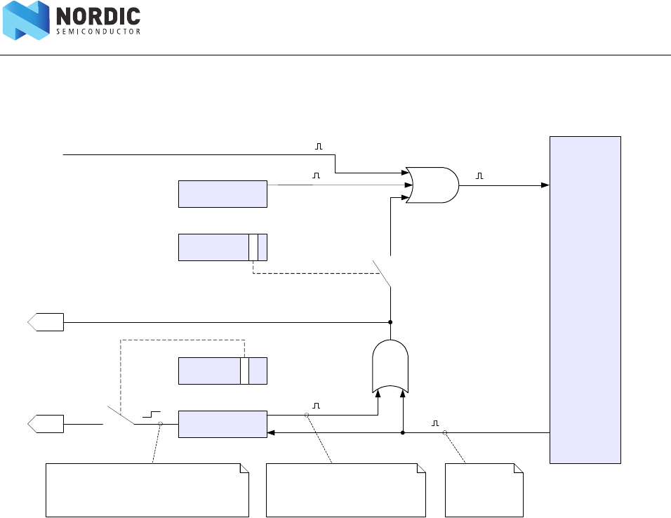
Figure 5 Tasks, events, shortcuts, and interrupts
9.1 Functional description
All peripherals on nRF51 series devices can be accessed through the standard ARM® Cortex Advanced
Peripheral Bus (APB) and AMBA High-performance Bus (AHB) registers as well as through task, event, and
interrupt registers.
9.1.1 Peripheral ID
For peripherals on the APB bus there is a direct relationship between its ID and its base address.
Every peripheral is assigned a fixed block of 0x1000 bytes, that is, a total of 1024 registers of 4 bytes on the
APB bus. The peripheral with base address 0x40000000 is therefore assigned ID=0, and a peripheral with the
base address 0x40001000 is assigned ID=1. The peripheral with the base address 0x4001F000 is assigned
ID=31.
Peripheral
core
TASK n
SHORTS k
EVENT m
From PPI
CPU write
INTEN m
To PPI
To NVIC
To core
From core
CPU write
Events and tasks
are pulses.
This signal reflects the state of the ”EVENT m” register,
i.e. if ”EVENT m” is ’1', the signal to the NVIC is ’1'; if
”EVENT m” is ’0', the signal to the NVIC is ’0'
The ability to trigger events from the CPU
is an optional feature, and may not be
implemented by all devices in the series.

Page 35 of 195
nRF51 Series Reference Manual v2.0 - Peripheral interface
Peripherals may share the same ID, which may impose one or more of the following limitations:
• Peripherals do not share any registers or common resources, but the total number of
registers available for each peripheral is reduced compared to a peripheral that has a
dedicated ID.
• Peripherals share some registers or other common resources.
• Only one of the peripherals can be used at a time.
• Both peripherals are optional in the series, and only one of them is instantiated in any given
chip.
9.1.2 Bit set and clear
Registers with multiple single-bit bit-fields may implement the “set and clear” pattern. This pattern enables
firmware to set and clear individual bits in a register without having to perform a read-modify-write
operation on the main register. This pattern is implemented using three consecutive addresses in the
register map where the main register is followed by a dedicated SET and CLR register in that order. The SET
register is used to set individual bits in the main register while the CLR register is used to clear individual bits
in the main register. Writing a ‘1’ to a bit in the SET or CLR register will set or clear the same bit in the main
register respectively. Reading the SET or CLR registers returns the value of the main register.
9.1.3 Tasks
Tasks are used to trigger actions in a peripheral, for example, to start a particular behavior. A peripheral can
implement multiple tasks with each task having a separate register in that peripheral’s task register group.
A task is triggered when firmware writes a ‘1’ to the task register or when the peripheral itself, or another
peripheral, toggles the corresponding task signal, see Figure 5 on page 34. All tasks follow the register layout
in Table 10 on page 37.
9.1.4 Events
Events are used to notify peripherals and the CPU about events that have happened, for example, a state
change in a peripheral. A peripheral may generate multiple events with each event having a separate
register in that peripheral’s event register group.
An event is generated when the peripheral itself toggles the corresponding event signal, whereupon the
event register is updated to reflect that the event has been generated, see Figure 5 on page 34. An event
register is only cleared when firmware writes a ‘0’ to it.
Events can be generated by the peripheral even when the event register is set to ‘1’. All events follow the
register layout described in Table 10 on page 37.
9.1.5 Shortcuts
A shortcut is a direct connection between an event and a task within the same peripheral. If a shortcut is
enabled, its associated task is automatically triggered when its associated event is generated.
Using a shortcut is the equivalent to making the same connection outside the peripheral and through the
PPI. However, the propagation delay through the shortcut is usually shorter than the propagation delay
through the PPI.
Shortcuts are predefined, which means their connections cannot be configured by firmware. Each shortcut
can be individually enabled or disabled through the shortcut register, one bit per shortcut, giving a

Page 36 of 195
nRF51 Series Reference Manual v2.0 - Peripheral interface
maximum of 32 shortcuts for each peripheral. All shortcut registers follow the register layout described in
Table 10 on page 37, (SHORTS).
9.1.6 Interrupts
An interrupt is an exception that is generated by an event and can interrupt the program flow of the CPU. All
peripherals on the APB bus support interrupts. A peripheral only occupies one interrupt, and the interrupt
number follows the peripheral ID, for example, the peripheral with ID=4 is connected to interrupt number 4
in the Nested Vector Interrupt Controller (NVIC).
Using the INTEN register, you can configure every event in a peripheral to generate that peripheral’s
interrupt. You can enable multiple events to generate interrupts simultaneously. To resolve the correct
interrupt’s source, firmware can query the event registers found in the event group in the peripherals
register map.
Each event implemented in the peripheral is associated with a specific bit position in the INTEN register. The
correct bit position can be derived from the event’s address. The event on address 0x100 is associated with
bit 0 in the INTEN register, the event at address 0x104 is associated with bit 1, and so on. The event at
address 0x17C is identified with bit 31 in the INTEN register. This pattern effectively limits the maximum
number of events in a peripheral to 32.
The INTEN register implements the “set and clear” pattern, which is illustrated in Table 10 on page 37, that is,
INTEN, INTENSET, and INTENCLR. The relationship between tasks, events, shortcuts, and interrupts is shown
in Figure 5 on page 34.

Page 37 of 195
nRF51 Series Reference Manual v2.0 - Peripheral interface
9.2 Register overview tables
All peripherals follow the register group pattern in Table 10; tasks are grouped together, events are grouped
together, and all other register types are grouped together. In addition, SHORTS and INTEN registers have a
fixed location in the register map.
Table 10 Example of register overview table
Register Offset Description
TASKS
{TASK0} 0x000 Description of the first task
{TASK1} 0x004 Description of the second task
<>
{TASK31} 0x07C Description of the 32nd task (last task)
EVENTS
{EVENT0} 0x100 Description of the first event
{EVENT1} 0x104 Description of the second event
<>
{EVENT31} 0x17C Description of the 32nd event (last event)
REGISTERS
SHORTS 0x200 Shortcut register
INTENSET 0x304 Interrupt enable set register
INTENCLR 0x308 Interrupt enable clear register
{REG0} 0x400 First generic register
<> <> <>
{REGN} 0x7FC Last generic register
Page 38 of 195
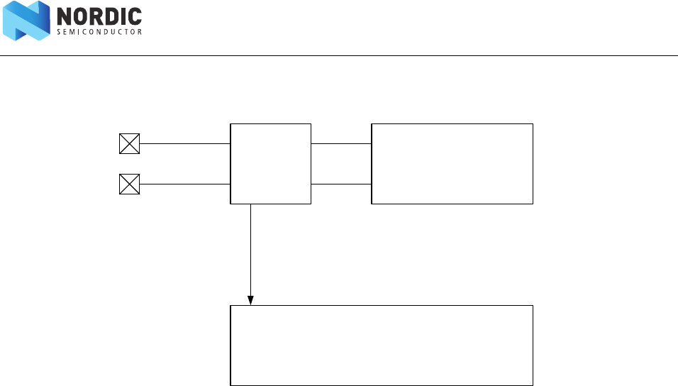
nRF51 Series Reference Manual v2.0 - Debugger Interface (DIF)
10 Debugger Interface (DIF)
Figure 6 Debugger interface
10.1 Functional description
nRF51 devices support the Serial wire Debug (SWD) interface from ARM. The interface has two lines;
SWDCLK and SWDIO. SWDIO and nRESET share the same physical pin. The Debugger Interface (DIF) module
is responsible for handling the resource sharing between SWD traffic and reset functionality. The SWDCLK pin
has an internal pull down resistor and the SWDIO/nRESET pin has an internal pull up resistor.
10.1.1 Normal mode
The DIF module will be in normal mode after power on reset. In this mode the SWDIO/nRESET pin acts as a
normal active low reset pin.
To guarantee that the device remains in normal mode, the SWDCLK line must be held low, that is, '0', at all
times. Failing to do so may result in the DIF entering into an unknown state and may lead to undesirable
behavior and power consumption.
10.1.2 Debug interface mode
Debug interface mode is initiated by clocking one clock cycle on SWDCLK with SWDIO=1. Due to delays
caused by starting up the DAP's power domain, a minimum of 150 clock cycles must be clocked at a speed
of minimum 125 kHz on SWDCLK with SWDIO=1 to guaranty that the DAP is able to capture a minimum of
50 clock cycles.
If the device is in System OFF mode, see the POWER chapter, Chapter 11 “Power management (POWER)” on
page 40, for more information about System OFF mode, entering into debug interface mode will generate a
wake-up.
In debug interface mode, the SWDIO/nRESET pin will be used as SWDIO. The pin reset mechanism will
therefore be disabled as long as the device is in debug interface mode.
In debug interface mode, System OFF will be emulated to facilitate debugging of the device while in System
OFF. Power numbers will naturally be higher in emulated System OFF compared to normal System OFF. See
emulated System OFF in Chapter 11 “Power management (POWER)” on page 40 for more information.
DIF
SWDCLK
SWDIO / nRESET
DAP
ARM CoreSigth
TM
DAP-Lite
SWDCLK
SWDIO
POWER
nRESET

Page 39 of 195
nRF51 Series Reference Manual v2.0 - Debugger Interface (DIF)
10.1.3 Resuming normal mode
Normal mode can always be resumed by performing a "hard-reset" through the SWD interface:
1. Enter debug interface mode.
2. Enable reset through the RESET register in the POWER peripheral.
3. Hold the SWDCLK and SWDIO/nRESET line low for a minimum of 100 µs.
You can also generate a "hard-reset" by performing a power on reset, or a brown-out reset.
Page 40 of 195
nRF51 Series Reference Manual v2.0 - Power management (POWER)
11 Power management (POWER)
The power management on the nRF51 series gives you unique flexibility through the orthogonal power
control of all system blocks on the devices.
11.1 Functional description
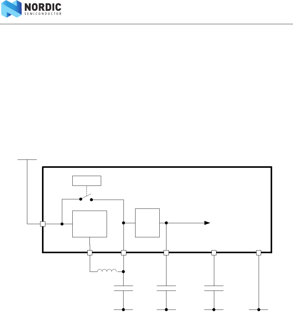
11.1.1 Power supply
The nRF51 supports three different power supply alternatives: internal DC/DC converter setup, internal LDO
setup, and Low Voltage mode setup.
11.1.1.1 DC/DC converter setup
Selected nRF51 series devices have a Buck type DC/DC converter that steps down the supply voltage VDD.
The resulting voltage is then used by an internal LDO that supplies the system with power, see Figure 7.
Figure 7 DC/DC converter
The DC/DC converter requires an external LC filter and is enabled through the DCDCEN register as illustrated
in Figure 7. See the product specification for more information about component values.
The DC/DC converter only reduces the system's net power consumption if VDD is above the minimum
voltage (stated in the product specification) and the internal current consumption (IDD) gives a DC/DC
conversion factor of FDCDC < 1. Therefore, to save power it is recommended to disable the DC/DC converter
if VDD is below the minimum voltage or FDCDC > 1.
AVDD is connected to VDD internally if the DC/DC converter is not enabled. This internal connection
introduces a small series resistance between VDD and AVDD, see the product specification for more
information.
nRF51
DC/DC
Converter
VDD
DCC AVDD
L
GND
C
LDO
DEC2 DEC1
GND
C
GND
C
System power
DCDCEN
VDD
VSS
GND
Page 41 of 195
nRF51 Series Reference Manual v2.0 - Power management (POWER)
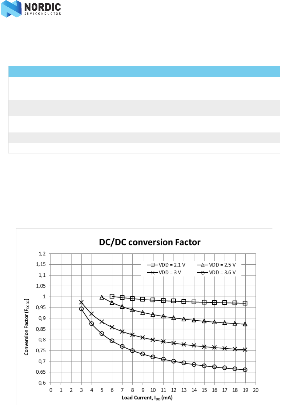
Calculating current when the DC/DC converter is enabled
The device current consumption when the DC/DC converter is enabled (IDD,DCDC) can be calculated using
Equation 1, the parameters in Table 11 and the conversion factor chart in Figure 7 on page 40.
Table 11 DC/DC current calculation parameters
Equation 1 DC/DC current calculation
The internal current consumption (IDD), calculated using electrical specification data from the product
specification, is used with the supply voltage (VDD) to find the current factor (FDCDC) using Figure 8.
Figure 8 DC/DC conversion factor
Parameter Description Value
IDD Internal current consumption (current drawn
from device power regulators) under Normal Test
Conditions (NTC)
Calculated by adding current values
from Electrical Specification tables in
the device product specification.
IDD,DCDC Current drawn from the external power supply
(VDD) when the DC/DC converter is enabled
Calculated using Equation 1.
FDCDC DC/DC current conversion factor based on DC/DC
converter efficiency
Interpolated from Figure 7.
VDD Voltage at VDD pin
TSTART,DCDC DC/DC converter startup time. Calculated using Equation 2.
IDD DCDCFDCDC IDD
=

Page 42 of 195
nRF51 Series Reference Manual v2.0 - Power management (POWER)
If FDCDC < 1, then IDD,DCDC < IDD when the DC/DC converter is enabled, resulting in a decrease in power
consumption.
If FDCDC > 1, then IDD < IDD,DCDC when the DC/DC converter is enabled, resulting in an increase in power
consumption. This is due to the base run current of the DC/DC converter (IDCDC) being the dominant factor.
Continuous use of the DC/DC converter
Using the DC/DC converter continuously can save power when average load current is expected to be larger
than 4 to 6 mA. When average load current is less than 4 mA, the conversion factor FDCDC approaches a
value > 1 and continuous use of the DC/DC converter will increase current consumption.
For example, if a battery voltage VDD = 3V and an average internal current consumption, including the DC/
DC converter run current (IDCDC), is IDD = 10 mA: FDCDC would be 0.8 using Figure 7 on page 40.The current
drawn from VDD, when the DC/DC converter is enabled, would be IDD,DCDC = 0.8 x 10 mA = 8 mA.
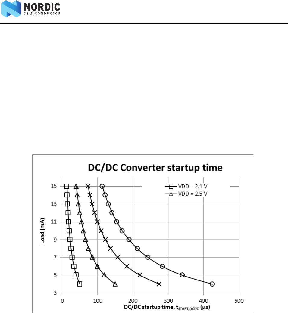
Page 43 of 195
nRF51 Series Reference Manual v2.0 - Power management (POWER)
Non-continuous use of the DC/DC converter
The DC/DC converter has a startup time of tSTART,DCDC. This is the time it takes for the DC/DC converter to
pull down AVDD to the internal supply voltage of 1.9 V. This is a function of the decoupling capacitance on
the AVDD pin (CAVDD), supply voltage (VDD), and load current (IDD):
Equation 2 DC/DC converter startup time
For example, given a decoupling capacitance (CAVDD) of 1 µF, supply voltage (VDD) of 3.6 V, and internal
current consumption (IDD) of 4 mA, tSTART,DCDC is 425 µs.
Figure 9 DC/DCconverterstartuptimewhenCAVDD=1 μf
tSTART,DCDC must be considered when enabling the DC/DC converter during periods of peak current
consumption because the DC/DC converter will draw base current of IDCDC when enabled, including the
startup period.
tSTART DCDC
VDD 1.9–CAVDD
IDD
-----------------------------------------------------
=
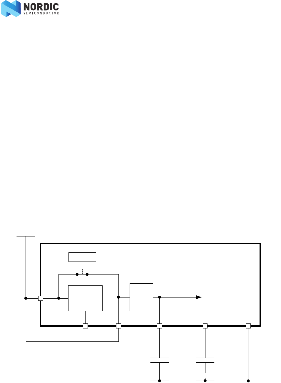
Page 44 of 195
nRF51 Series Reference Manual v2.0 - Power management (POWER)
For example, if the DC/DC converter was enabled and VDD = 3V and peak current IDD = 10 mA, FDCDC would
be 0.8 using Figure 8 on page 41 and tSTART,DCDC would be 110 µs using Equation 2 on page 43. The current
drawn from the battery in the first 110 µs would be IDD = 10 mA + (IDCDC) = 10.3mA. The current drawn from
the battery after the first 110 µs would be IDD,DCDC = 8.24 mA. Peak current, in this case, would have to be
drawn for more than 198 µs to save power:
Note: • If the DC/DC converter is to be used when the Radio is enabled, it must start (AVDD = 1.9V)
before the TXENABLE or RXENABLE tasks can be set. The DC/DC converter cannot be
enabled within tSTART,DCDC of the Radio starting. The software managing the non-continu-
ous use of the DC/DC converter must ensure this is true.
•The DC/DC converter does not operate over the whole device voltage range and must be
disabled (switching the device to use the internal LDO) when the voltage drops to the lower
threshold of the supply voltage range.
11.1.1.2 Internal LDO setup
The internal DC/DC converter can be bypassed if it is not going to be used. When the DC/DC converter is
bypassed, only the internal LDO is active as illustrated in Figure 10. The internal LDO will then generate the
system power directly from the supply voltage VDD. It is recommended that the DC/DC converter is
disabled in this setup.
Figure 10 LDO regulator only
8.24mA 110s
10.3mA
----------------------------------------110s+198s=
nRF51
DC/DC
Converter
VDD
DCC AVDD
DCDCEN
DEC2 DEC1
GND
C
GND
C
VDD
LDO
System power
VSS
GND
Page 45 of 195
nRF51 Series Reference Manual v2.0 - Power management (POWER)
11.1.1.3 Low voltage mode setup
If you have a stable, low voltage available for the nRF51 device, it is possible to configure the device in low
voltage mode as illustrated in Figure 11. In this mode the internal LDO is bypassed and the system is
powered directly from the supply voltage VDD. See the product specification for more information about
which voltage levels are supported in low voltage mode. In low voltage mode, the DC/DC converter must be
disabled. Additional requirements may apply to the accuracy and stability of the supply voltage in low
voltage mode. See the product specification for more information.
Figure 11 Low voltage mode
11.1.2 System OFF mode
System OFF is the deepest power saving mode the system can enter. In this mode, the system’s core
functionality is powered down and all ongoing tasks are terminated. The only mechanism that is functional
and responsive in this mode is the reset and the wake-up mechanism.
One or more blocks of RAM can be retained in System OFF mode depending on the settings in the RAMON
register.
The system can be woken up from System OFF mode either from the DETECT signal generated by the GPIO
peripheral, by the ANADETECT signal generated by the LPCOMP module, or from a reset. When the system
wakes up from OFF mode, a system reset is performed.
Before entering System OFF mode you must make sure that all on-going EasyDMA transactions have been
completed. This is usually accomplished by making sure that the EasyDMA enabled peripheral is not active
when entering System OFF.
11.1.2.1 Emulated System OFF mode
If the device is in debug interface mode, System OFF will be emulated to secure that all required resources
needed for debugging are available during System OFF, see Chapter 10 “Debugger Interface (DIF)” on
nRF51
DC/DC
Converter
VDD
DCC AVDD
DCDCEN
DEC2 DEC1
GND
C
GND
C
VDD
LDO
System power
VSS
GND

Page 46 of 195
nRF51 Series Reference Manual v2.0 - Power management (POWER)
page 38, for more information. This includes the following key components: DAP, DIF, CLOCK, POWER,
NVMC, MPU, CPU, CODE, and RAM. Since the CPU is kept on in emulated System OFF mode, it is
recommended to add an infinite loop directly after entering System OFF, to prevent the CPU from executing
code that normally should not be executed.
11.1.3 System ON mode
System ON mode is a fully operational mode, where the CPU and selected peripherals can be brought into a
state where they are functional and more or less responsive depending on the sub power mode selected.
In System ON mode the CPU can either be active or sleeping. The CPU enters sleep by executing the WFI or
WFE instruction found in the CPU’s instruction set. In WFI sleep the CPU will wake up as a result of an
interrupt request if the associated interrupt is enabled in the NVIC. In WFE sleep the CPU will wake up as a
result of an interrupt request regardless of the associated interrupt being enabled in the NVIC or not.
The system implements mechanisms to automatically switch on and off the appropriate power sources
depending on how many peripherals are active, and how much power is needed at any given time. The
power requirement of a peripheral is directly related to its activity level. The activity level is usually raised
and lowered when specific tasks are triggered or events generated, see individual chapters describing the
different peripherals for more information on how to optimize power consumption in System ON mode.
11.1.3.1 Sub power modes
During CPU sleep, in System ON mode, the system can reside in one of the following two sub power modes:
•Constant Latency
•Low Power
In Constant Latency mode (for more information, see the device specific product specification) the CPU
wakeup latency and the PPI task response will be constant and kept at a minimum. This is secured by forcing
a set of base resources while in sleep, see the device specific product specification for more information
about which resources are forced on. The advantage of having a constant and predictable latency will be at
the cost of having increased power consumption. The Constant Latency mode is selected by triggering the
CONSTLAT task.
In Low Power mode the automatic power management system, described in Section 11.1.3 “System ON
mode”, will be most effective and save most power. The advantage of having low power will be at the cost of
having varying CPU wakeup latency and PPI task response. The Low Power mode is selected by triggering
the LOWPWR task.
When the system enters ON mode, it will, by default, reside in the Low Power sub power mode.
Page 47 of 195
nRF51 Series Reference Manual v2.0 - Power management (POWER)
11.1.4 Power supply supervisor
The power supply supervisor initializes the system at power-on and provides an early warning of impending
power failure. In addition the power supply supervisor puts the system in a reset state if the supply voltage
is too low for safe operation (brown-out). The power supply supervisor is illustrated in Figure 12.
Figure 12 Power supply supervisor
11.1.4.1 Power-fail comparator
The power failure comparator provides the CPU with an early warning of impending power failure. It will not
reset the system, but give the CPU time to prepare for an orderly power-down. It also provides hardware
protection of data stored in program memory by preventing write and erase instructions from being
executed.
The comparator has approximately 0.1 V of hysteresis (VHYST), as illustrated in Figure 13.
Figure 13 Power failure comparator (BOR = Brown-out reset)
POFCON
MUX
THRESHOLD
2.1V
2.3V
2.5V
2.7V
POFWARN
1.7V Brown-out reset
Power on reset
C
R
VSS
VDD
VDD
t
MCU
POFWARN
THRESHOLD
THRESHOLD+VHYST
POFWARN
1.7V
BOR

Page 48 of 195
nRF51 Series Reference Manual v2.0 - Power management (POWER)
The power failure comparator is only intended to be used as long as the CPU is running. If the power failure
comparator is enabled when the CPU is not running, this may result in unpredictable behavior in the power
failure comparator.
11.1.5 RAM blocks
Each of the available RAM blocks, which each may contain multiple RAM sections, can power up and down
independently in both System ON and System OFF mode. See Chapter 4 “Memory” on page 11 for more
information about RAM blocks and their sections.
11.1.6 Reset
The nRF51 series implements various reset sources. After a reset the CPU can query the RESETREAS (reset
reason register) to find out which source generated the reset.
11.1.6.1 Power-on reset
The power-on reset generator initializes the system at power-on. The system is held in reset state until the
supply has reached the minimum operating voltage, see the device specific product specification for more
information.
11.1.6.2 Pin reset
A pin reset is generated when the physical reset pin on the device is asserted. Since the debugger interface
uses the same pin as the pin reset mechanism, a pin reset will not be available when the device is in debug
interface mode unless explicitly enabled in the RESET register.
11.1.6.3 Wakeup from OFF mode reset
The device is reset when it wakes up from OFF mode.
The DAP is not reset following a wake up from OFF mode if the device is in debug interface mode, see
Chapter 10 “Debugger Interface (DIF)” on page 38 for more information.
11.1.6.4 Soft reset
A soft reset is generated when the SYSRESETREQ bit of the Application Interrupt and Reset Control Register
(AIRCR register) in the ARM® core is set.
11.1.6.5 Watchdog reset
A Watchdog reset is generated when the watchdog times out.
11.1.6.6 Brown-out reset
The brown-out reset generator puts the system in reset state if the supply voltage drops below the brown-
out reset threshold.
11.1.6.7 Retained registers
A retained register is a register that will retain its value in System OFF mode, and through a reset depending
on reset source. See individual peripheral chapters for information of which registers are retained for the
different peripherals.

Page 49 of 195
nRF51 Series Reference Manual v2.0 - Power management (POWER)
11.1.6.8 Reset behavior
11.2 Registers
Table 12 Register overview
Reset source
Reset target
CPU Peripherals GPIO DAP RAM1
1. The RAM is never reset, but depending on reset source, RAM content may be corrupted.
WDT Retained
registers RESETREAS
CPU lockup2
2. Reset from CPU lockup is disabled if the device is in debug interface mode. CPU lockup is not possible in System OFF.
Soft reset
Wakeup from System OFF
mode reset
3
3. The DAP will not be reset if the device is in debug interface mode.
4
4. RAM is not reset on wake-up from OFF mode, but depending on settings in the RAMON register parts, or the whole RAM, may
not be retained after the device has entered System OFF mode.
Watchdog reset5
5. Watchdog reset is not available in System OFF.
Pin reset6
6. Not available when device is in debug interface mode.
Brownout reset
Power on reset
Register Offset Description
TASKS
CONSTLAT 0x078 Enable constant latency mode
LOWPWR 0x07C Enable low power mode (variable latency)
EVENTS
POFWARN 0x108 Power failure warning
REGISTERS
INTENSET 0x304 Interrupt enable set register
INTENCLR 0x308 Interrupt enable clear register
RESETREAS 0x400 Reset reason
SYSTEMOFF 0x500 System OFF register
POFCON 0x510 Power failure configuration
GPREGRET 0x51C General purpose retention register
RAMON 0x524 RAM on/off
RESET 0x544 Configure reset functionality
DCDCEN 0x578 DCDC enable register

Page 50 of 195
nRF51 Series Reference Manual v2.0 - Power management (POWER)
11.2.1 RESETREAS
Unless cleared, this register is cumulative. A field is cleared by writing ‘1’ to it. If none of the reset sources are
flagged, it indicates that the chip was reset from the on-chip reset generator.
11.2.2 SYSTEMOFF
11.2.3 GPREGRET
Bit number 31 30 29 28 27 26 25 24 23 22 21 20 19 18 17 16 15 14 13 12 11 10 9 8 7 6 5 4 3 2 1 0
ID (Field ID) - - - - - - - - - - - - - G F E - - - - - - - - - - - - D C B A
Reset value 0 0 0 0 0 0 0 0 0 0 0 0 0 0 0 0 0 0 0 0 0 0 0 0 0 0 0 0 0 0 0 0
ID RW Field Value ID Value Description
A RW RESETPIN 1 Reset from pin detected
BRW DOG 1Reset from watchdog detected
C RW SREQ 1 Reset from AIRCR.SYSRESETREQ detected
DRW LOCKUP 1Reset from CPU lock-up detected
E RW OFF 1 Reset due to wake-up from OFF mode when wakeup is triggered from the
DETECT signal from GPIO
FRW LPCOMP 1Reset due to wake-up from OFF mode when wakeup is triggered from
ANADETECT signal from LPCOMP
G RW DIF 1 Reset due to wake-up from OFF mode when wakeup is triggered from entering
into debug interface mode
Bit number 31 30 29 28 27 26 25 24 23 22 21 20 19 18 17 16 15 14 13 12 11 10 9 8 7 6 5 4 3 2 1 0
ID (Field ID) - - - - - - - - - - - - - - - - - - - - - - - - - - - - - - - A
Reset value 0 0 0 0 0 0 0 0 0 0 0 0 0 0 0 0 0 0 0 0 0 0 0 0 0 0 0 0 0 0 0 0
ID RW Field Value ID Value Description
A W 1 Enter System OFF mode
Bit number 31 30 29 28 27 26 25 24 23 22 21 20 19 18 17 16 15 14 13 12 11 10 9 8 7 6 5 4 3 2 1 0
ID (Field ID) ------------------------AAAAAAAA
Reset value 00000000000000000000000000000000
ID RW Field Value ID Value Description
A RW General purpose retention register. This register is a retained register.

Page 51 of 195
nRF51 Series Reference Manual v2.0 - Power management (POWER)
11.2.4 POFCON
11.2.5 RAMON
The RAM is divided into separate blocks for power management purposes. These blocks are not related in
any way to the region concept described in the memory chapter.
Bit number 31 30 29 28 27 26 25 24 23 22 21 20 19 18 17 16 15 14 13 12 11 10 9 8 7 6 5 4 3 2 1 0
ID (Field ID) - - - - - - - - - - - - - - - - - - - - - - - - - - - - - B B A
Reset value 0 0 0 0 0 0 0 0 0 0 0 0 0 0 0 0 0 0 0 0 0 0 0 0 0 0 0 0 0 0 0 0
ID RW Field Value
ID Value Description
A RW POF 0 Disable power failure comparator
1Enable power failure comparator
B RW THRESHOLD V21 0 Set threshold to 2.1 V
V23 1Set threshold to 2.3 V
V25 2 Set threshold to 2.5 V
V27 3Set threshold to 2.7 V
Bit number 31 30 29 28 27 26 25 24 23 22 21 20 19 18 17 16 15 14 13 12 11 10 9 8 7 6 5 4 3 2 1 0
ID (Field ID) - - - - - - - - - - - - H G F E - - - - - - - - - - - - D C B A
Reset value 0 0 0 0 0 0 0 0 0 0 0 0 0 0 0 0 0 0 0 0 0 0 0 0 0 0 0 0 1 1 1 1
ID RW Field Value ID Value Description
A RW ONRAM0 0 Keep RAM block 0 off in ON mode
1Keep RAM block 0 on in ON mode
B RW ONRAM1 0 Keep RAM block 1 off in ON mode
1Keep RAM block 1 on in ON mode
C RW ONRAM2 0 Keep RAM block 2 off in ON mode
1Keep RAM block 2 on in ON mode
D RW ONRAM3 0 Keep RAM block 3 off in ON mode
1Keep RAM block 3 on in ON mode
E RW OFFRAM0 0 Keep RAM block 0 off in OFF mode
1Keep RAM block 0 on in OFF mode
F RW OFFRAM1 0 Keep RAM block 1 off in OFF mode
1Keep RAM block 1 on in OFF mode
G RW OFFRAM2 0 Keep RAM block 2 off in OFF mode
1Keep RAM block 2 on in OFF mode
H RW OFFRAM3 0 Keep RAM block 3 off in OFF mode
1Keep RAM block 3 on in OFF mode

Page 52 of 195
nRF51 Series Reference Manual v2.0 - Power management (POWER)
11.2.6 RESET
11.2.7 DCDCEN
Bit number 31 30 29 28 27 26 25 24 23 22 21 20 19 18 17 16 15 14 13 12 11 10 9 8 7 6 5 4 3 2 1 0
ID (Field ID) - - - - - - - - - - - - - - - - - - - - - - - - - - - - - - - A
Reset value 0 0 0 0 0 0 0 0 0 0 0 0 0 0 0 0 0 0 0 0 0 0 0 0 0 0 0 0 0 0 0 1
ID RW Field Value ID Value Description
A RW Enable pin reset in debug interface mode, see the DIF peripheral register. This
register is a retained register.
0Disable
1Enable
Bit number 31 30 29 28 27 26 25 24 23 22 21 20 19 18 17 16 15 14 13 12 11 10 9 8 7 6 5 4 3 2 1 0
ID (Field ID) - - - - - - - - - - - - - - - - - - - - - - - - - - - - - - - A
Reset value 0 0 0 0 0 0 0 0 0 0 0 0 0 0 0 0 0 0 0 0 0 0 0 0 0 0 0 0 0 0 0 0
ID RW Field Value ID Value Description
ARW Enable DC/DC converter.
0Disable
1Enable
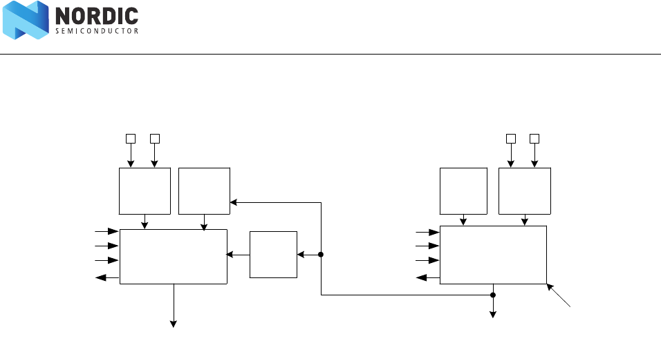
Page 53 of 195
nRF51 Series Reference Manual v2.0 - Clock management (CLOCK)
12 Clock management (CLOCK)
Figure 14 Clock control
12.1 Functional description
The system depends on, and generates, two different clocks: a high frequency clock (HFCLK) and a low
frequency clock (LFCLK). These clocks are only available when the system is in ON mode.
The HFCLK is fixed to 16 MHz and the LFCLK is fixed to 32.768 kHz.
12.1.1 Low frequency clock (LFCLK)
The system supports three LFCLK clock sources: the 32.768 kHz crystal oscillator, the 32.768 kHz RC
oscillator, and the 32.768 kHz synthesized clock, see Figure 14. The 32.768 kHz crystal oscillator requires an
external AT-cut quartz crystal to be connected to the XL1 and XL2 pins in parallel resonant mode. The XL1
and XL2 share pins with the GPIO.
Note: GPIOs that share pins with XL1 and XL2 differ from device to device. For more information, see
the device specific product specification.
The LFCLK clock and all of the available LFCLK sources are switched off by default when the system is
propagated from OFF to ON mode.
The LFCLK clock is started by first selecting the preferred clock source in the LFCLKSRC register and then
triggering the LFCLKSTART task. If the selected clock source cannot be started immediately the 32.768 kHz
RC oscillator will start automatically and generate the LFCLK until the selected clock source is available.
The LFCLK is stopped by triggering the LFCLKSTOP task. The LFCLKSRC register should only be modified
when the LFCLK is not running.
The 32.768 kHz crystal oscillator utilizes an amplitude regulated architecture to achieve low current
consumption and fast start-up. The 32.768 kHz crystal oscillator is also designed to work with one of the
following alternative external sources:
• A rail-to-rail clock signal applied to the XL1 pin. The XL2 pin shall then be left unconnected.
• A low swing clock signal applied to the XL1 pin. The XL2 pin shall then be left unconnected.
32.768 kHz
RC
oscillator
32.768 kHz
crystal
oscillator
16 MHz
RC
oscillator
16/32 MHz
crystal
oscillator
LFCLK
clock control
HFCLK
clock control
HFCLK
LFCLK
LFCLKSRC
LFCLKSTART
LFCLKSTOP
LFCLKSTARTED
HFCLKSTART
HFCLKSTOP
HFCLKSTARTED
Request from the
rest of the system
XL1 XL2 XC1 XC2
32.768 kHz
synthesizer
HFCLKSRC

Page 54 of 195
nRF51 Series Reference Manual v2.0 - Clock management (CLOCK)
The synthesized 32.768 kHz clock depends on the HFCLK to run. If 250 ppm accuracy is required for the
LFCLK running off the synthesized 32.768 kHz clock, the HFCLK must be generated from the 16/32 MHz
crystal oscillator.
12.1.2 High frequency clock (HFCLK)
The system supports two high frequency clock sources: the 16/32 MHz crystal oscillator and the 16 MHz RC
oscillator, see Figure 14 on page 53. The HFCLK (16/32 MHz) crystal oscillators require an external AT-cut
quartz crystal to be connected to the XC1 and XC2 pins in parallel resonant mode. If a 32 MHz crystal is used
the XTALFREQ register must be configured accordingly.
When the system enters ON mode, the 16 MHz RC oscillator will start up automatically to provide the HFCLK
to the CPU and other active parts of the system.
The HFCLK crystal oscillator is started by triggering the HFCLKSTART task and stopped using the HFCLKSTOP
task. A HFCLKSTARTED event will be generated when the selected HFCLK crystal oscillator has started. The
start-up times of the 16 MHz and 32 MHz crystal oscillators are described in the device specific product
specification.
The 16 MHz RC oscillator is automatically switched off when one of the HFCLK crystal oscillators is running; it
will be switched back on automatically when the HFCLK crystal oscillator is stopped.
If the system does not require a 16 MHz clock, the 16 MHz RC oscillator may be switched off automatically to
save power. This occurs if all peripherals that require the HFCLK are appropriately stopped or disabled, and
the CPU is sleeping. When this condition is no longer met the 16 MHz RC oscillator is automatically restarted.
These optimization steps are only performed when the HFCLK is generated from the 16 MHz RC oscillator.
To use the RADIO and the calibration mechanism associated with the 32.768 kHz RC oscillator, the HFCLK
must be generated from a HFCLK crystal oscillator.
The HFCLK crystal oscillators utilize amplitude regulated architecture to achieve low current consumption
and fast start-up. The HFCLK crystal oscillators are also designed to work with one of the following
alternative external sources:
• A 16 MHz rail-to-rail clock signal applied to the XC1 pin. The XC2 pin shall then be left
unconnected.
• A 16MHz low swing clock signal applied to the XC1 pin. The XC2 pin shall then be left
unconnected.
12.1.3 Calibrating the 32.768 kHz RC oscillator
After the 32.768 kHz RC oscillator is started and running, it can be calibrated triggering the CAL task. The
32.768 kHz RC oscillator will then temporarily request the HFCLK to calibrate itself against. A DONE event
will be generated when calibration has finished. The calibration mechanism will only work as long as HFCLK
is generated from the 16/32MHz crystal oscillator. Therefore, it is necessary to explicitly start this crystal
oscillator before calibration can be started. See the device product specification for recommendations on
calibration intervals and crystal accuracy.
12.1.3.1 Calibration timer
The calibration timer can be used to time the calibration interval of the 32.768 kHz RC oscillator. The
calibration timer is started by triggering the CTSTART task and stopped by triggering the CTSTOP task. The
calibration timer will always start counting down from the value specified in CTIV and generate a CTTO
timeout event when it reaches 0. The Calibration timer will stop by itself when it reaches 0.

Page 55 of 195
nRF51 Series Reference Manual v2.0 - Clock management (CLOCK)
Figure 15 Calibration timer
Due to limitations in the calibration timer, only one task related to calibration, that is, CAL, CTSTART and
CTSTOP, can be triggered for every period of LFCLOCK.
12.2 Registers
Table 13 Register overview
Register Offset Description
TASKS
HFCLKSTART 0x000 Start HFCLK crystal oscillator
HFCLKSTOP 0x004 Stop HFCLK crystal oscillator
LFCLKSTART 0x008 Start LFCLK source
LFCLKSTOP 0x00C Stop LFCLK source
CAL 0x010 Start calibration of LFCLK RC oscillator
CTSTART 0x014 Start calibration timer
CTSTOP 0x018 Stop calibration timer
EVENTS
HFCLKSTARTED 0x100 16 MHz oscillator started
LFCLKSTARTED 0x104 32 kHz oscillator started
DONE 0x10C Calibration of LFCLK RC oscillator complete event
CTTO 0x110 Calibration timer timeout
REGISTERS
INTENSET 0x304 Interrupt enable set register
INTENCLR 0x308 Interrupt enable clear register
HFCLKSTAT 0x40C Which HFCLK source is running
LFCLKSTAT 0x418 Which LFCLK source is running
LFCLKSRC 0x518 Clock source for the 32 kHz clock
CTIV 0x538 Calibration timer interval
XTALFREQ 0x550 Crystal frequency
Calibration
timer
CTSTART
CTSTOP
CTTO
CTIV

Page 56 of 195
nRF51 Series Reference Manual v2.0 - Clock management (CLOCK)
12.2.1 HFCLKSTAT
12.2.2 LFCLKSRC
12.2.3 LFCLKSTAT
Bit number 31 30 29 28 27 26 25 24 23 22 21 20 19 18 17 16 15 14 13 12 11 10 9 8 7 6 5 4 3 2 1 0
ID (Field ID) - - - - - - - - - - - - - - - B - - - - - - - - - - - - - - - A
Reset value 0 0 0 0 0 0 0 0 0 0 0 0 0 0 0 0 0 0 0 0 0 0 0 0 0 0 0 0 0 0 0 0
ID RW Field Value ID Value Description
AR SRC Active Clock source
RC 016 MHz RC oscillator running and generating the HFCLK
XTAL 1 16/32 MHz crystal oscillator running and generating the HFCLK
B R STATE HFCLK state
HFCLK not running
HFCLK running
NOTRUNNING 0
RUNNING 1
Bit number 31 30 29 28 27 26 25 24 23 22 21 20 19 18 17 16 15 14 13 12 11 10 9 8 7 6 5 4 3 2 1 0
ID (Field ID) ------------------------------AA
Reset value 00000000000000000000000000000000
ID RW Field Value ID Value Description
ARW SRC Clock source
RC 032.768 kHz RC oscillator
XTAL 1 32.768 kHz crystal oscillator
SYNTH 232.768 kHz synthesizer synthesizing 32.768 kHz from 16 MHz system clock
Bit number 31 30 29 28 27 26 25 24 23 22 21 20 19 18 17 16 15 14 13 12 11 10 9 8 7 6 5 4 3 2 1 0
ID (Field ID) - - - - - - - - - - - - - - - B - - - - - - - - - - - - - - A A
Reset value 0 0 0 0 0 0 0 0 0 0 0 0 0 0 0 0 0 0 0 0 0 0 0 0 0 0 0 0 0 0 0 0
ID RW Field Value ID Value Description
AR SRC Active Clock source
RC 032.768 kHz RC oscillator running and generating the LFCLK
XTAL 1 32.768 kHz crystal oscillator running and generating the LFCLK
SYNTH 232.768 kHz synthesizer synthesizing 32.768 kHz from 16 MHz system clock
BR STATE LFCLK state
NOTRUNNING 0LFCLK not running
RUNNING 1 LFCLK running

Page 57 of 195
nRF51 Series Reference Manual v2.0 - Clock management (CLOCK)
12.2.4 CTIV
12.2.5 XTALFREQ
Bit number 31 30 29 28 27 26 25 24 23 22 21 20 19 18 17 16 15 14 13 12 11 10 9 8 7 6 5 4 3 2 1 0
ID (Field ID) 0 0 0 0 0 0 0 0 0 0 0 0 0 0 0 0 0 0 0 0 0 0 0 0 0 A A A A A A A
Reset value 0 0 0 0 0 0 0 0 0 0 0 0 0 0 0 0 0 0 0 0 0 0 0 0 0 0 0 0 0 0 0 0
ID RW Field Value ID Value Description
A RW Calibration timer interval in multiples of 0.25 seconds.
Range: 0.25 seconds to 31.75 seconds.
Bit number 31 30 29 28 27 26 25 24 23 22 21 20 19 18 17 16 15 14 13 12 11 10 9 8 7 6 5 4 3 2 1 0
ID (Field ID) - - - - - - - - - - - - - - - - - - - - - - - - A A A A A A A A
Reset value 1 1 1 1 1 1 1 1 1 1 1 1 1 1 1 1 1 1 1 1 1 1 1 1 1 1 1 1 1 1 1 1
ID RW Field Value ID Value Description
A RW Select nominal frequency of external crystal for HFCLK. This register has to match the actual
crystal used in design to enable correct behavior.
0xFF 16 MHz crystal is used.
0x00 32 MHz crystal is used.
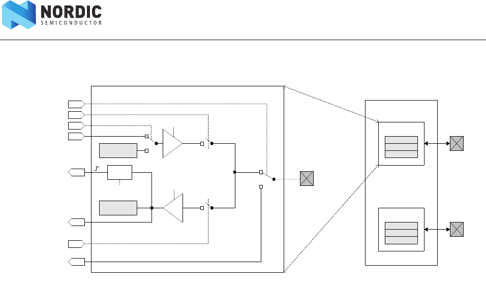
Page 58 of 195
nRF51 Series Reference Manual v2.0 - GPIO
13 GPIO
Figure 16 GPIO Port and the GPIO pin details
Figure 16 illustrates the GPIO port containing 32 individual pins, where PIN0 is illustrated in more detail as a
reference. All the signals on the left side of the illustration are used by other peripherals in the system, and
therefore, are not directly available to the CPU.
13.1 Functional description
The GPIO Port peripheral implements up to 32 pins, PIN0 through PIN31. Each of these pins can be
individually configured in the PIN_CNF[n] registers (n=0..31). The following parameters can be configured
through these registers:
•Direction
•Drive strength
• Enabling of pull-up and pull-down resistors
• Pin sensing
• Input buffer disconnect
• Analog input (for selected pins)
The PIN[n].CNF registers are retained registers. See Chapter 11 “Power management (POWER)” on page 40
for more information about retained registers.
Pins can be individually configured, through the pin sense mechanism, to detect either a high level or a low
level on their input. When the correct level is detected, the sense mechanism raises the DETECT signal line,
which can then be read by other peripherals in the system, see Figure 16. This mechanism is functional in
both ON and OFF mode.
The input buffer of a GPIO pin can be disconnected from the pin to enable power savings when the pin is
not used as an input, see Figure 16. Inputs must be connected in order to get a valid input value in the IN
register and for the sense mechanism to get access to the pin.
Other peripherals in the system can attach themselves to GPIO pins and override their output value and
configuration, or read their analog or digital input value, see Figure 16.
GPIO Port
PIN31
PIN0
PIN31
PIN_CNF[31]
IN.31
OUT.31
PIN0
PIN_CNF[0]
IN.0
OUT.0
..
PIN0
OUT.0
IN.0
IN
Sense
OUT_OVERRIDE
DIR_OVERRIDE
DETECT
OUT
O
I
O: output buffer I: input buffer
PIN_CNF[0].INPUT
PIN_CNF[0].PULL
PIN_CNF[0].DRIVE
PIN0_CNF.SENSE
PIN_CNF[0].DIR
INPUT_OVERRIDE
ANAIN
ANAEN

Page 59 of 195
nRF51 Series Reference Manual v2.0 - GPIO
Selected PINs also support analog input signals, see ANAIN in Figure 16 on page 58. Pins that support
analog input signals vary between devices, see the product specification for your device for more details.
Pin direction can be configured both in the DIR register as well as through the individual PIN_CNF[n]
registers. A change in one register will automatically be reflected in the other register.
13.2 Registers
Table 14 Register overview
13.2.1 OUT
13.2.2 IN
Register Offset Description
REGISTERS
OUT 0x504 Write GPIO port
OUTSET 0x508 Set individual bits in GPIO port
OUTCLR 0x50C Clear individual bits in GPIO port
IN 0x510 Read GPIO port
DIR 0x514 Direction of GPIO pins
DIRSET 0x518 Setting DIR register
DIRCLR 0x51C Clearing DIR register
PIN_CNF[0] 0x700 Configuration of pin 0
.. .. ..
PIN_CNF[31] 0x77C Configuration of pin 31
Bit number 31 30 29 28 27 26 25 24 23 22 21 20 19 18 17 16 15 14 13 12 11 10 9 8 7 6 5 4 3 2 1 0
ID (Field ID) AAAAAAAAAAAAAAAAAA AAAAAAAAAAAAAA
Reset value 000000000000000000 00000000000000
ID RW Field Value ID Value Description
A RW Register to write to the whole GPIO port. Bit position in register relates to pin
number in GPIO port, e.g. bit 0 relates to GPIO pin number 0.
Bit number 31 30 29 28 27 26 25 24 23 22 21 20 19 18 17 16 15 14 13 12 11 10 9 8 7 6 5 4 3 2 1 0
ID (Field ID) AAAAAAAAAAAAAAAAAAAAAAAAAAAAAAAA
Reset value 00000000000000000000000000000000
ID RW Field Value ID Value Description
A R Register to read the whole GPIO port. Bit position in register relates to pin number
in GPIO port, e.g. bit 0 relates to GPIO pin number 0.

Page 60 of 195
nRF51 Series Reference Manual v2.0 - GPIO
13.2.3 OUTSET
13.2.4 OUTCLR
13.2.5 DIR
13.2.6 DIRSET
Bit number 31 30 29 28 27 26 25 24 23 22 21 20 19 18 17 16 15 14 13 12 11 10 9876543210
ID (Field ID) AAAAAAAAAAAAAAAAAAAAAAAAAAAAAAAA
Reset value 00000000000000000000000000000000
ID RW Field Value ID Value Description
A RW Register to set pins in the GPIO port high (‘1’). Bit position in register relates to pin
number in GPIO port, e.g. bit 0 relates to GPIO pin number 0. Setting a ‘1’ in one of
the bits in the register will set the corresponding bit in the GPIO port high.
Bit number 31 30 29 28 27 26 25 24 23 22 21 20 19 18 17 16 15 14 13 12 11 10 9 8 7 6 5 4 3 2 1 0
ID (Field ID) AAAAAAAAAAAAAAAAAAAAAAAAAAAAAAAA
Reset value 00000000000000000000000000000000
ID RW Field Value ID Value Description
A RW Register to clear pins in the GPIO port low (‘0’). Bit position in register relates to pin
number in GPIO port, e.g. bit 0 relates to GPIO pin number 0. Setting a ‘1’ in one of
the bits in the register will set the corresponding bit in the GPIO port low.
Bit number 31 30 29 28 27 26 25 24 23 22 21 20 19 18 17 16 15 14 13 12 11 10 9 8 7 6 5 4 3 2 1 0
ID (Field ID) AAAAAAAAAAAAAAAAAAAAAAAAAAAAAAAA
Reset value 00000000000000000000000000000000
ID RW Field Value ID Value Description
A RW Register to set direction of pins in the GPIO. Bit position in register relates to pin
number in GPIO port, e.g. bit 0 relates to GPIO pin number 0. Setting a ‘1’ in one of
the bits in the register will configure the corresponding GPIO pin as an output pin.
Setting the same bit to ‘0’ will configure GPIO pin as an input.
Bit number 31 30 29 28 27 26 25 24 23 22 21 20 19 18 17 16 15 14 13 12 11 10 9 8 7 6 5 4 3 2 1 0
ID (Field ID) A A A A A A A A A A A A A A A A A A A A A A A A A A A A A A A A
Reset value 0 0 0 0 0 0 0 0 0 0 0 0 0 0 0 0 0 0 0 0 0 0 0 0 0 0 0 0 0 0 0 0
ID RW Field Value ID Value Description
A RW Register to set individual bits in the DIR register, which subsequently sets
individual GPIO pins as outputs. Setting a ‘1’ in one or more bits in this register will
set the corresponding bits in the DIR register.

Page 61 of 195
nRF51 Series Reference Manual v2.0 - GPIO
13.2.7 DIRCLR
13.2.8 PIN_CNF[n] (n=0..31)
Bit number 31 30 29 28 27 26 25 24 23 22 21 20 19 18 17 16 15 14 13 12 11 10 9 8 7 6 5 4 3 2 1 0
ID (Field ID) A A A A A A A A A A A A A A A A A A A A A A A A A A A A A A A A
Reset value 0 0 0 0 0 0 0 0 0 0 0 0 0 0 0 0 0 0 0 0 0 0 0 0 0 0 0 0 0 0 0 0
ID RW Field Value ID Value Description
A RW Register to clear individual bits in the DIR register, which subsequently sets
individual GPIO pins as input. Setting a ‘1’ in one or more bits in this register will
clear the corresponding bits in the DIR register.
Bit number 31 30 29 28 27 26 25 24 23 22 21 20 19 18 17 16 15 14 13 12 11 10 9 8 7 6 5 4 3 2 1 0
ID (Field ID) - - - - - - - - - - - - - - E E - - - - - D D D - - - - C C B A
Reset value 0 0 0 0 0 0 0 0 0 0 0 0 0 0 0 0 0 0 0 0 0 0 0 0 0 0 0 0 0 0 1 0
ID RW Field Value ID Value Description
ARWDIR Pin direction
INPUT 0Configure pin as an input pin
OUTUT 1 Configure pin as an output pin
BRW INPUT Connect or disconnect input buffer
CONNECT 0 Connect input buffer
DISCONNECT 1Disconnect input buffer
CRWPULL
DISABLED 0No pull
PULLDOWN 1 Pull down on pin
PULLUP 3Pull up on pin
DRWDRIVE
S0S1 0Standard 0, standard 1
H0S1 1 High drive 0, standard 1
S0H1 2Standard 0, high drive 1
H0H1 3 High drive 0, high drive 1
D0S1 4Disconnect 0, standard 1
D0H1 5 Disconnect 0, high drive 1
S0D1 6Standard 0, disconnect 1
H0D1 7 High drive 0, disconnect 1
ERW SENSE Pin sensing mechanism
DISABLED 0 Disabled
HIGH 2Sense for high level
LOW 3 Sense for low level

Page 62 of 195
nRF51 Series Reference Manual v2.0 - GPIO tasks and events (GPIOTE)
14 GPIO tasks and events (GPIOTE)
14.1 Functional description
The GPIO Tasks and Events (GPIOTE) module provides functionality for accessing GPIO pins using tasks and
events.
A task can be used for performing the following write operations to a pin:
•Set
•Clear
• Toggle
An event can be generated from any of the following input pins using the GPIO DETECT signal:
• Rising edge
•Falling edge
•Any change
14.1.1 Pin events and tasks
The GPIOTE module has a number of tasks and events that can be configured to operate on individual GPIO
pins; the OUT[n] tasks and the IN[n] events. The tasks can be used for writing to individual pins, and the
events can be generated from changes occurring at the inputs of individual pins.
The tasks and events are configured using the CONFIG[n] registers. Every pair of OUT[n] tasks and IN[n]
events has one CONFIG[n] register associated with it.
When an OUT[n] task or an IN[n] event has been configured to operate on a pin, the pin can only be written
from the GPIOTE module. Attempting to write a pin as a normal GPIO pin will have no effect.
As long as an OUT[n] task or an IN[n] event is configured to control a pin n, the pin's output value will only be
updated by the GPIOTE module. The pin's output value as specified in the GPIO will therefore be ignored as
long as the pin is controlled by GPIOTE. When the GPIOTE is disconnected from a pin, see MODE field in
CONFIG[n] register, the associated pin will get the output and configuration values specified in the GPIO
module.
When a GPIOTE channel is configured to operate on a pin as a task, the initial value of that pin is configured
in the OUTINIT field of CONFIG[n].
14.1.2 Port event
PORT is an event that can be generated from multiple input pins using the GPIO DETECT signal. The event
will be generated on the rising edge of the DETECT signal. See Section 13.1 “Functional description” on
page 58 for more information about the DETECT signal.
This feature is always enabled although the peripheral itself appears to be IDLE, that is, no clocks or other
power intensive infrastructure have to be requested to keep this feature enabled. This feature can therefore
be used to wake-up the CPU from a WFI or WFE type sleep in System ON with all peripherals and the CPU
idle, that is, lowest power consumption in System ON mode.

Page 63 of 195
nRF51 Series Reference Manual v2.0 - GPIO tasks and events (GPIOTE)
14.2 Registers
Table 15 Register overview
Registers Offset Description
TASKS
OUT[0] 0x000 Task for writing to pin specified by PSEL in CONFIG[0].
OUT[1] 0x004 Task for writing to pin specified by PSEL in CONFIG[1].
OUT[2] 0x008 Task for writing to pin specified by PSEL in CONFIG[2].
OUT[3] 0x00C Task for writing to pin specified by PSEL in CONFIG[3].
EVENTS
IN[0] 0x100 Event generated from pin specified by PSEL in CONFIG[0].
IN[1] 0x104 Event generated from pin specified by PSEL in CONFIG[1].
IN[2] 0x108 Event generated from pin specified by PSEL in CONFIG[2].
IN[3] 0x10C Event generated from pin specified by PSEL in CONFIG[3].
PORT 0x17C Event generate from multiple input pins.
REGISTERS
INTENSET 0x304 Interrupt enable set register.
INTENCLR 0x308 Interrupt enable clear register.
CONFIG[0] 0x510 Configuration for OUT[0] task and IN[0] event.
CONFIG[1] 0x514 Configuration for OUT[1] task and IN[1] event.
CONFIG[2] 0x518 Configuration for OUT[2] task and IN[2] event.
CONFIG[3] 0x51C Configuration for OUT[3] task and IN[3] event.

Page 64 of 195
nRF51 Series Reference Manual v2.0 - GPIO tasks and events (GPIOTE)
14.2.1 CONFIG[n] (n=0..3)
Bit number 31 30 29 28 27 26 25 24 23 22 21 20 19 18 17 16 15 14 13 12 11 10 9 8 7 6 5 4 3 2 1 0
ID (Field ID) - - - - - - - - - - - D - - C C - - - B B B B B - - - - - - A A
Reset value 0 0 0 0 0 0 0 0 0 0 0 0 0 0 0 0 0 0 0 0 0 0 0 0 0 0 0 0 0 0 0 0
ID RW Field Value ID Value Description
ARW MODE Mode
DISABLED 0Disabled. Pin specified by PSEL will not be acquired by the GPIOTE module.
EVENT 1 Event mode. The pin specified by PSEL will be configured as an input and the
IN[n] event will be generated if operation specified in POLARITY occurs on the
pin.
TASK 3Task mode. The pin specified by PSEL will be configured as an output and
triggering the OUT[n] task will perform the operation specified by POLARITY on
the pin. When enabled as a task the GPIOTE module will acquire the pin and the
pin can no longer be written as a regular output pin from the GPIO module.
B RW PSEL [0..31] Pin number associated with OUT[n] task and IN[n] event.
CRW POLARITY When in task mode: Operation to be performed on output when OUT[n] task is
triggered.
When In event mode: Operation on input that shall trigger IN[n] event.
LOTOHI 1 Task mode: Set pin from OUT[n] task.
Event mode: Generate IN[n] event when rising edge on pin.
HITOLO 2Task mode: Clear pin from OUT[n] task.
Event mode: Generate IN[n] event when falling edge on pin.
TOGGLE 3 Task mode: Toggle pin from OUT[n].
Event mode: Generate IN[n] when any change on pin.
DRW OUTINIT When in task mode: Initial value of the output when the GPIOTE channel is
configured.
When in event mode: No effect.
LOW 0Task mode: Initial value of pin before task triggering is low.
HIGH 1 Task mode: Initial value of pin before task triggering is high.
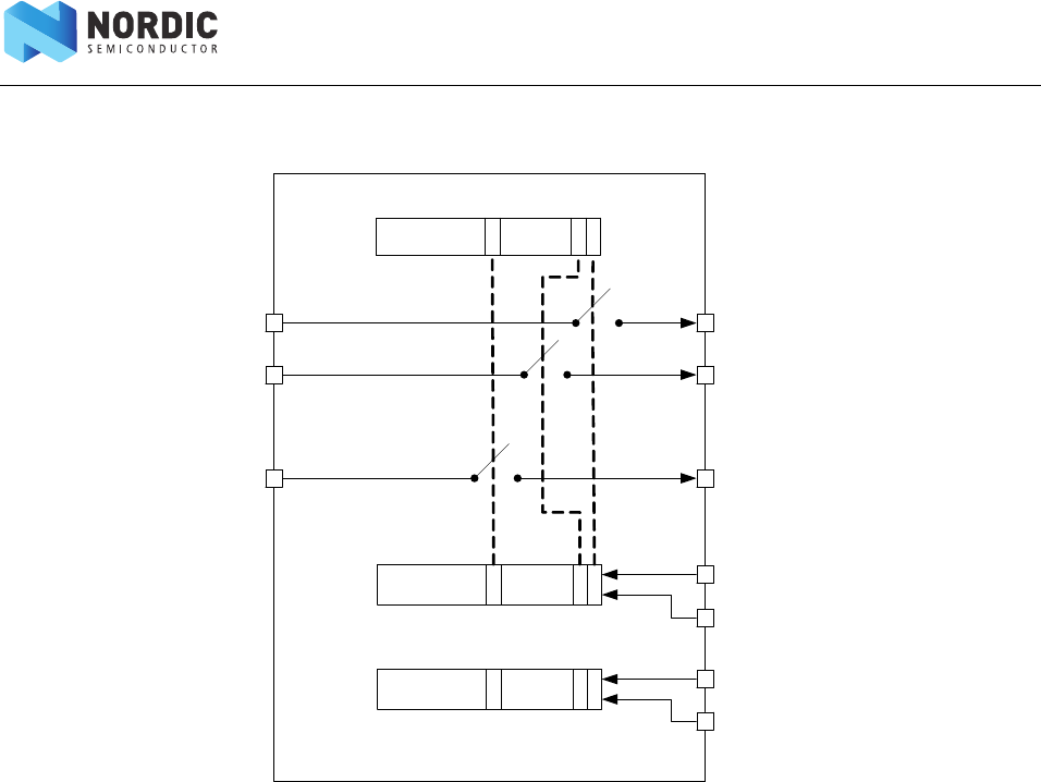
Page 65 of 195
nRF51 Series Reference Manual v2.0 - Programmable Peripheral Interconnect (PPI)
15 Programmable Peripheral Interconnect (PPI)
Figure 17 PPI block diagram
15.1 Functional description
The Programmable Peripheral Interconnect (PPI) enables peripherals to interact autonomously with each
other using tasks and events independent of the CPU.
The PPI provides a mechanism to automatically trigger a task in one peripheral as a result of an event
occurring in another peripheral. A task is connected to an event through a PPI channel. The PPI channel is
composed of two end-point registers, the Event End-Point (EEP) and the Task End-Point (TEP). A peripheral
task is connected to a Task End-Point using the address of the task register associated with the task.
Similarly, a peripheral event is connected to an Event End-Point using the address of the event register
associated with the event.
There are two ways of enabling and disabling PPI channels:
• Enable or disable PPI channels individually using the CHEN, CHENSET, and CHENCLR
registers.
• Enable or disable PPI channels in PPI channel Groups through the Groups’ ENABLE and
DISABLE tasks. Prior to these tasks being triggered, the PPI channel Group must be
configured to define which PPI channels belongs to which groups.
01n
01n
CH[0].EEP
CH[1].EEP
CH[n].EEP
CH[0].TEP
CH[1].TEP
CH[n].TEP
CHG[0].EN
CHG[0].DIS
CHG[m].EN
CHG[m].DIS
n: number of channels
m: number of channel groups
CHG[0]
CHG[m]
01n
CHEN

Page 66 of 195
nRF51 Series Reference Manual v2.0 - Programmable Peripheral Interconnect (PPI)
PPI tasks (for example, CHG0EN) can be triggered through the PPI like any other task, which means they can
be hooked up to a PPI channel as a TEP. One event can trigger multiple tasks by using multiple channels and
one task can be triggered by multiple events in the same way.
15.1.1 Pre-programmed channels
The PPI system has in addition to the fully programmable peripheral interconnections, a set of channels
where the event (EEP) and task (TEP) endpoints are set in hardware. These fixed channels can be individually
enabled, disabled, or added to PPI channel groups in the same way as ordinary PPI channels.
Table 16 Pre-programmed channels
15.2 Registers
Channel EEP TEP
20 TIMER0->EVENTS_COMPARE[0] RADIO->TASKS_TXEN
21 TIMER0->EVENTS_COMPARE[0] RADIO->TASKS_RXEN
22 TIMER0->EVENTS_COMPARE[1] RADIO->TASKS_DISABLE
23 RADIO->EVENTS_BCMATCH AAR->TASKS_START
24 RADIO->EVENTS_READY CCM->TASKS_KSGEN
25 RADIO->EVENTS_ADDRESS CCM->TASKS_CRYPT
26 RADIO->EVENTS_ADDRESS TIMER0->TASKS_CAPTURE[1]
27 RADIO->EVENTS_END TIMER0->TASKS_CAPTURE[2]
28 RTC0->COMPARE[0] RADIO-> TASKS_TXEN
29 RTC0->COMPARE[0] RADIO-> TASKS_RXEN
30 RTC0->COMPARE[0] TIMER0->TASKS_CLEAR
31 RTC0->COMPARE[0] TIMER0->TASKS_START
Register Offset Description
TASKS
CHG[0].EN 0x000 Enable channel group 0
CHG[0].DIS 0x004 Disable channel group 0
CHG[1].EN 0x008 Enable channel group 1
CHG[1].DIS 0x00C Disable channel group 1
CHG[2].EN 0x010 Enable channel group 2
CHG[2].DIS 0x014 Disable channel group 2
CHG[3].EN 0x018 Enable channel group 3
CHG[3].DIS 0x01C Disable channel group 3
REGISTERS
CHEN 0x500 Channel enable
CHENSET 0x504 Channel enable set
CHENCLR 0x508 Channel enable clear
CH[0].EEP 0x510 Channel 0 event endpoint
CH[0].TEP 0x514 Channel 0 task endpoint

Page 67 of 195
nRF51 Series Reference Manual v2.0 - Programmable Peripheral Interconnect (PPI)
CH[1].EEP 0x518 Channel 1 event endpoint
CH[1].TEP 0x51C Channel 1 task endpoint
CH[2].EEP 0x520 Channel 2 event endpoint
CH[2].TEP 0x524 Channel 2 task endpoint
CH[3].EEP 0x528 Channel 3 event endpoint
CH[3].TEP 0x52C Channel 3 task endpoint
CH[4].EEP 0x530 Channel 4 event endpoint
CH[4].TEP 0x534 Channel 4 task endpoint
CH[5].EEP 0x538 Channel 5 event endpoint
CH[5].TEP 0x53C Channel 5 task endpoint
CH[6].EEP 0x540 Channel 6 event endpoint
CH[6].TEP 0x544 Channel 6 task endpoint
CH[7].EEP 0x548 Channe 7 event endpoint
CH[7].TEP 0x54C Channel 7 task endpoint
CH[8].EEP 0x550 Channel 8 event endpoint
CH[8].TEP 0x554 Channel 8 task endpoint
CH[9].EEP 0x558 Channel 9 event endpoint
CH[9].TEP 0x55C Channel 9 task endpoint
CH[10].EEP 0x560 Channel 10 event endpoint
CH[10].TEP 0x564 Channel 10 task endpoint
CH[11].EEP 0x568 Channel 11 event endpoint
CH[11].TEP 0x56C Channel 11 task endpoint
CH[12].EEP 0x570 Channel 12 event endpoint
CH[12].TEP 0x574 Channel 12 task endpoint
CH[13].EEP 0x578 Channel 13 event endpoint
CH[13].TEP 0x57C Channel 13 task endpoint
CH[14].EEP 0x580 Channel 14 event endpoint
CH[14].TEP 0x584 Channel 14 task endpoint
CH[15].EEP 0x588 Channel 15 event endpoint
CH[15].TEP 0x58C Channel 15 task endpoint
CHG[0] 0x800 Channel group 0
CHG[1] 0x804 Channel group 1
CHG[2] 0x808 Channel group 2
CHG[3] 0x80C Channel group 3
Register Offset Description

Page 68 of 195
nRF51 Series Reference Manual v2.0 - Programmable Peripheral Interconnect (PPI)
15.2.1 CHEN
Bit number 31 30 29 28 27 26 25 24 23 22 21 20 19 18 17 16 15 14 13 12 11 10 9 8 7 6 5 4 3 2 1 0
ID (Field ID) FF EE DD CC BB AA Z Y X W V U - - - - P O N M L K J I H G F E D C B A
Reset value 0 0 0 0 0 0 0 0 0 0 0 0 0 0 0 0 0 0 0 0 0 0 0 0 0 0 0 0 0 0 0 0
ID RW Field Value ID Value Description
AR
W
CH0 Enable or disable channel 0
0Disable
1Enable
B.. CH1 .. ..
C .. CH2 .. ..
D.. CH3 .. ..
E .. CH4 .. ..
F.. CH5 .. ..
G.. CH6 ..
H.. CH7 .. ..
I .. CH8 .. ..
J.. CH9 .. ..
K..CH10 .. ..
L.. CH11 .. ..
M.. CH12 .. ..
N.. CH13 .. ..
O.. CH14 .. ..
P.. CH15 .. ..
U.. CH20 .. ..
V.. CH21 .. ..
W.. CH22 .. ..
X.. CH23 .. ..
Y..CH24 .. ..
Z.. CH25 .. ..
AA .. CH26 .. ..
BB CH27 .. ..
CC CH28 .. ..
DD CH29 .. ..
EE CH30 .. ..
FF CH31 .. ..

Page 69 of 195
nRF51 Series Reference Manual v2.0 - Programmable Peripheral Interconnect (PPI)
15.2.2 CHENSET
Bit number 31 30 29 28 27 26 25 24 23 22 21 20 19 18 17 16 15 14 13 12 11 10 9 8 7 6 5 4 3 2 1 0
ID (Field ID) FF EE DD CC BB AA Z Y X W V U - - - - P O N M L K J I H G F E D C B A
Reset value 0 0 0 0 0 0 0 0 0 0 0 0 0 0 0 0 0 0 0 0 0 0 0 0 0 0 0 0 0 0 0 0
ID RW Field Value ID Value Description
A CH0 Enable channel 0
W 1 Enable
R CHEN.CH0 Read value of CH0 field in CHEN register
B.. CH1 .. ..
C.. CH2 .. ..
D.. CH3 .. ..
E.. CH4 .. ..
F.. CH5 .. ..
G.. CH6 .. ..
H.. CH7 .. ..
I..CH8 .. ..
J.. CH9 .. ..
K.. CH10 .. ..
L.. CH11 .. ..
M.. CH12 .. ..
N.. CH13 .. ..
O.. CH14 .. ..
P.. CH15 .. ..
U.. CH20 .. ..
V.. CH21 .. ..
W.. CH22 .. ..
X.. CH23 .. ..
Y.. CH24 .. ..
Z.. CH25 .. ..
AA .. CH26 .. ..
BB .. CH27 .. ..
CC .. CH28 .. ..
DD .. CH29 .. ..
EE .. CH30 .. ..
FF .. CH31 .. ..

Page 70 of 195
nRF51 Series Reference Manual v2.0 - Programmable Peripheral Interconnect (PPI)
15.2.3 CHENCLR
Bit number 31 30 29 28 27 26 25 24 23 22 21 20 19 18 17 16 15 14 13 12 11 10 9 8 7 6 5 4 3 2 1 0
ID (Field ID) FF EE DD CC BB AA Z Y X W V U - - - - P O N M L K J I H G F E D C B A
Reset value 0 0 0 0 0 0 0 0 0 0 0 0 0 0 0 0 0 0 0 0 0 0 0 0 0 0 0 0 0 0 0 0
ID RW Field Value ID Value Description
A CH0 Enable channel 0
W 1 Enable
R CHEN.CH0 Read value of CH0 field in CHEN register
B.. CH1 .. ..
C..CH2 .. ..
D.. CH3 .. ..
E..CH4 .. ..
F.. CH5 .. ..
G.. CH6 .. ..
H.. CH7 .. ..
I..CH8 .. ..
J.. CH9 .. ..
K..CH10 .. ..
L.. CH11 .. ..
M.. CH12 .. ..
N.. CH13 .. ..
O.. CH14 .. ..
P.. CH15 .. ..
U.. CH20 .. ..
V.. CH21 .. ..
W.. CH22 .. ..
X.. CH23 .. ..
Y..CH24 .. ..
Z.. CH25 .. ..
AA .. CH26 .. ..
BB .. CH27 .. ..
CC .. CH28 .. ..
DD .. CH29 .. ..
EE .. CH30 .. ..
FF .. CH31 .. ..

Page 71 of 195
nRF51 Series Reference Manual v2.0 - Programmable Peripheral Interconnect (PPI)
15.2.4 CH[n].EEP (n=0..15)
Event endpoints are only able to recognize addresses from the EVENT group.
15.2.5 CH[n].TEP (n=0..15)
Task endpoints are only able to recognize addresses from the TASK group.
Bit number 31 30 29 28 27 26 25 24 23 22 21 20 19 18 17 16 15 14 13 12 11 10 9 8 7 6 5 4 3 2 1 0
ID (Field ID) AAAAAAAAAAAAAAAAAAAAAAAAAAAAAAAA
Reset value 00000000000000000000000000000000
ID RW Field Value ID Value Description
A RW Pointer to event register. Accepts only addresses to registers from the Event
group.
Bit number 31 30 29 28 27 26 25 24 23 22 21 20 19 18 17 16 15 14 13 12 11 10 9 8 7 6 5 4 3 2 1 0
ID (Field ID) AAAAAAAAAAAAAAAAAAAAAAAAAAAAAAAA
Reset value 00000000000000000000000000000000
ID RW Field Value ID Value Description
A RW Pointer to task register. Accepts only addresses to registers from the Task group.

Page 72 of 195
nRF51 Series Reference Manual v2.0 - Programmable Peripheral Interconnect (PPI)
15.2.6 CHG[n] (n=0..3)
Bit number 31 30 29 28 27 26 25 24 23 22 21 20 19 18 17 16 15 14 13 12 11 10 9 8 7 6 5 4 3 2 1 0
ID (Field ID) FF EE DD CC BB AA Z Y X W V U - - - - P O N M L K J I H G F E D C B A
Reset value 0 0 0 0 0 0 0 0 0 0 0 0 0 0 0 0 0 0 0 0 0 0 0 0 0 0 0 0 0 0 0 0
ID RW Field Value ID Value Description
A RW CH0 Include or exclude channel 0 in group n
0Exclude
1Include
BRW CH1 .. ..
C RW CH2 .. ..
DRW CH3 .. ..
E RW CH4 .. ..
FRW CH5 .. ..
G RW CH6 .. ..
HRW CH7 .. ..
I RW CH8 .. ..
JRW CH9 .. ..
KRWCH10 .. ..
LRW CH11 .. ..
MRWCH12 .. ..
NRW CH13 .. ..
ORWCH14 .. ..
PRW CH15 .. ..
URWCH20 .. ..
VRW CH21 .. ..
WRWCH22 .. ..
XRW CH23 .. ..
YRWCH24 .. ..
ZRW CH25 .. ..
AA RW CH26 .. ..
BB RW CH27 .. ..
CC RW CH28 .. ..
DD RW CH29 .. ..
EE RW CH30 .. ..
FF RW CH31 .. ..
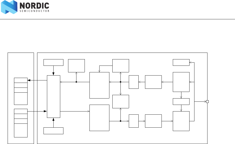
Page 73 of 195
nRF51 Series Reference Manual v2.0 - 2.4 GHz radio (RADIO)
16 2.4 GHz radio (RADIO)
Figure 18 Radio block diagram
The RADIO contains a 2.4 GHz radio receiver and a 2.4 GHz radio transmitter that is compatible with Nordic's
proprietary 2 Mbps, 1 Mbps, and 250 kbps radio modes in addition to 1 Mbps Bluetooth Low Energy mode.
The RADIO implements EasyDMA. EasyDMA in combination with an automated packet assembler and
packet disassembler, and an automated CRC generator and CRC checker, makes it very easy to configure
and use the RADIO. See Figure 18 for more information.
The RADIO includes a Device Address Match unit and an interframe spacing control unit that can be utilized
to simplify address white listing and interframe spacing respectively, in Bluetooth Low Energy and similar
applications.
The RADIO also includes a Received Signal Strength Indicator (RSSI) and a bit counter. The bit counter
generates events when a preconfigured number of bits have been sent or received by the RADIO.
16.1 Functional description
16.1.1 EasyDMA
The RADIO implements EasyDMA for reading and writing of data packets from and to the RAM without CPU
involvement.
As illustrated in Figure 18, the RADIO's EasyDMA utilizes the same PACKETPTR pointer for receiving packets
and transmitting packets. The CPU should therefore reconfigure this pointer every time the radio is switched
between transmit and receive mode. The MAXLEN register configures the maximum number of bytes that
can be transmitted or received by the RADIO within the same packet. This feature can be used to ensure that
the RADIO does not overwrite, or read beyond, the RAM assigned to the packet.
The EasyDMA is guaranteed to have finished accessing the RAM when the DISABLED event is generated.
RADIO
2.4Gz
Receiver
2.4GHz
Transm itter
RSSI
EasyDMA
Dewhi teni ng
Whi teni ng
IFS
contr ol unit
CRC
CRC
Address
match
Bit counter
RAM
L
S0
Payoad
S1
L
S0
S1
PACKETPTR
ANT0, ANT1
Packet
disassembler
Packet
assembler
Device
Address
match
Packet synch
Payload
MAXLEN

Page 74 of 195
nRF51 Series Reference Manual v2.0 - 2.4 GHz radio (RADIO)
16.1.2 Packet configuration
A radio packet contains the following fields: PREAMBLE, ADDRESS, LENGTH, S0, S1, PAYLOAD, and CRC. The
radio sends the different fields in the packet in the order they are shown in Figure 19, from left to right. The
preamble will be sent least significant bit first on-air.
Figure 19 On-air packet layout
The PREAMBLE is always one byte long taking the value 0xAA or 0x55 depending on the first ADDRESS bit
that is sent on air. If the first bit of the ADDRESS is 0 the preamble is set to 0xAA. Otherwise, the PREAMBLE is
set to 0x55.
Radio packets are stored in memory inside instances of a radio packet data structure as shown in Figure 20.
The PREAMBLE, ADDRESS and CRC fields are omitted in this data structure since they are added dynamically
when the packet is sent.
Figure 20 In-RAM representation of radio packet, S0, LENGTH, and S1 are optional
The byte ordering on air is always least significant byte first for the ADDRESS and PAYLOAD fields and most
significant byte first for the CRC field. The ADDRESS fields are always transmitted and received with least
significant bit first on-air. The CRC field is always transmitted and received with the most significant bit first.
The bit-endianness (which means the order the bits are sent and received in) of the S0, LENGTH, S1, and
PAYLOAD fields can be configured through the ENDIAN field in PCNF1.
The sizes of the S0, LENGTH, and S1 fields can be individually configured through S0S, LS, and S1S in PCNF0
respectively. If any of these fields are configured to be less than 8 bits long, the least significant bits of the
fields, as seen from the RAM representation, are used.
If S0, LENGTH, or S1 are specified with zero length, their fields will be omitted in memory. Otherwise, each
field is represented as a separate byte, regardless of the number of bits in their on-air counterpart.
16.1.3 Maximum packet length
Independent of the configuration of MAXLEN, the combined length of S0, LENGTH, S1, and PAYLOAD cannot
exceed 255 bytes.
16.1.4 Address configuration
The on-air radio ADDRESS field is composed of two parts: the base address field and the address prefix field,
see Figure 19. The size of the base address field is configurable through BALEN in PCNF1. The base address is
truncated from LSByte if the BALEN is less than 4.
PREAMBLE BASE PREFIX S0 LEN GTH S1 CRCPAYLOAD
0x55 = 10101010 : 1
0xAA= 01010101 : 0
LSBit
LSByte
?
MSByteLSByte
LSBit
ADDRESS
S0 LENGTH S1 PAYLOAD
0nLSByte

Page 75 of 195
nRF51 Series Reference Manual v2.0 - 2.4 GHz radio (RADIO)
The on-air addresses are defined in the BASEn and PREFIXn registers. For other radio address registers such
as the TXADDRESS, RXADDRESSES and RXMATCH registers, logical radio addresses ranging from 0 to 7 are
being used. The relationship between the on-air radio addresses and the logical addresses are described in
Table 17.
Table 17 Definition of logical addresses
16.1.5 Received Signal Strength Indicator (RSSI)
The radio implements a mechanism for measuring the power in the received radio signal. This feature is
called Received Signal Strength Indicator (RSSI).
Sampling of the received signal strength is started by using the RSSISTART task. The sample can be read
from the RSSISAMPLE register.
The sample period of the RSSI is defined by RSSIRESOLUTION, see the device specific product specification for
details. The RSSI sample will hold the average received signal strength during this sample period.
For the RSSI sample to be valid the radio has to be enabled in receive mode (RXEN task) and the reception
has to be started (READY event followed by START task).
16.1.6 Data whitening
The RADIO is able to do packet whitening and de-whitening, see WHITEEN in PCNF1 register for how to
enable whitening. When enabled, whitening and de-whitening are handled by the RADIO automatically as
packets are sent and received, that is, radio packets located in RAM will not be whitened.
The whitening word is generated using polynomial g(D) = D7 + D4 + 1, which then is XORed with the data
packet that is to be whitened, or de-whitened, see Figure 21.
Figure 21 Data whitening and de-whitening.
Logical
address
Base
address Prefix byte
0 BASE0 PREFIX0.AP0
1BASE1 PREFIX0.AP1
2 BASE1 PREFIX0.AP2
3BASE1 PREFIX0.AP3
4 BASE1 PREFIX1.AP4
5BASE1 PREFIX1.AP5
6 BASE1 PREFIX1.AP6
7BASE1 PREFIX1.AP7
++
Data in
Data out
Position 0 1 2 3 4 5 6
D
0
D
4
D
7
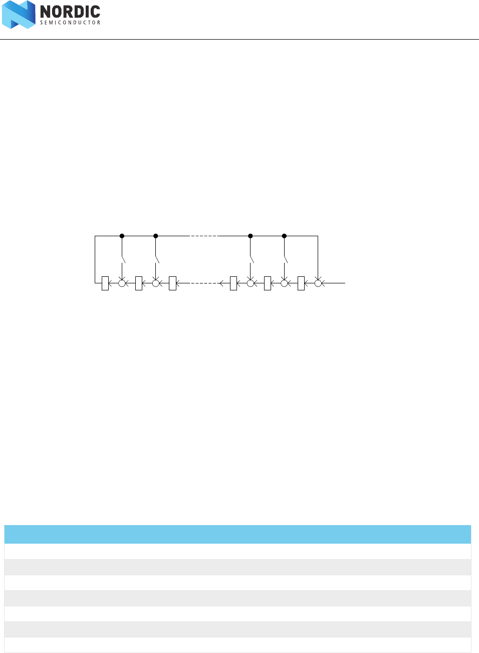
Page 76 of 195
nRF51 Series Reference Manual v2.0 - 2.4 GHz radio (RADIO)
Whitening and de-whitening will be performed over the whole packet, except for the preamble and the
address field.
The linear feedback shift register, illustrated in Figure 21 on page 75 can be initialized through the
DATAWHITEIV register.
16.1.7 CRC
The CRC generator in the RADIO calculates the CRC over the whole packet excluding the preamble. If
desirable the address field can be excluded from the CRC calculation as well, see CRCCNF register for more
information.
The CRC polynomial is configurable as illustrated in Figure 22 where bit 0 in the CRCPOLY register
corresponds to X0 and bit 1 corresponds to X1 etc. See CRCPOLY for more information.
Figure 22 CRC generator for an n bit CRC
As illustrated in Figure 17 on page 65, the CRC is calculated by feeding the packet serially through the CRC
generator. Before the packet is clocked through the CRC generator, the CRC generator's latches b0 through
bn will be initialized with a predefined value specified in the CRCINIT register. When the whole packet is
clocked through the CRC generator, latches b0 through bn will hold the resulting CRC. This value will be used
by the RADIO during both transmission and reception but it is not available to be read by the CPU at any
time. A received CRC can however be read by the CPU through the RXCRC register independent of whether
or not it has passed the CRC check.
The length (n) of the CRC is configurable, see CRCCNF for more information.
16.1.8 Radio states
The radio can enter the states described in Table 18.
Table 18 Radio states
State Description
DISABLED No operations are going on inside the radio and the power consumption is at a minimum.
RXRU The radio is ramping up and preparing for reception.
RXIDLE The radio is ready for reception to start.
RX Reception has been started and the addresses enabled in the RXADDRESSES register are being monitored.
TXRU The radio is ramping up and preparing for transmission.
TXIDLE The radio is ready for transmission to start.
TX The radio is transmitting a packet.
+
Packet
(Clocked in serially)
+
+
+
+
Xn
bnb0
Xn-1 X2 X1 X0
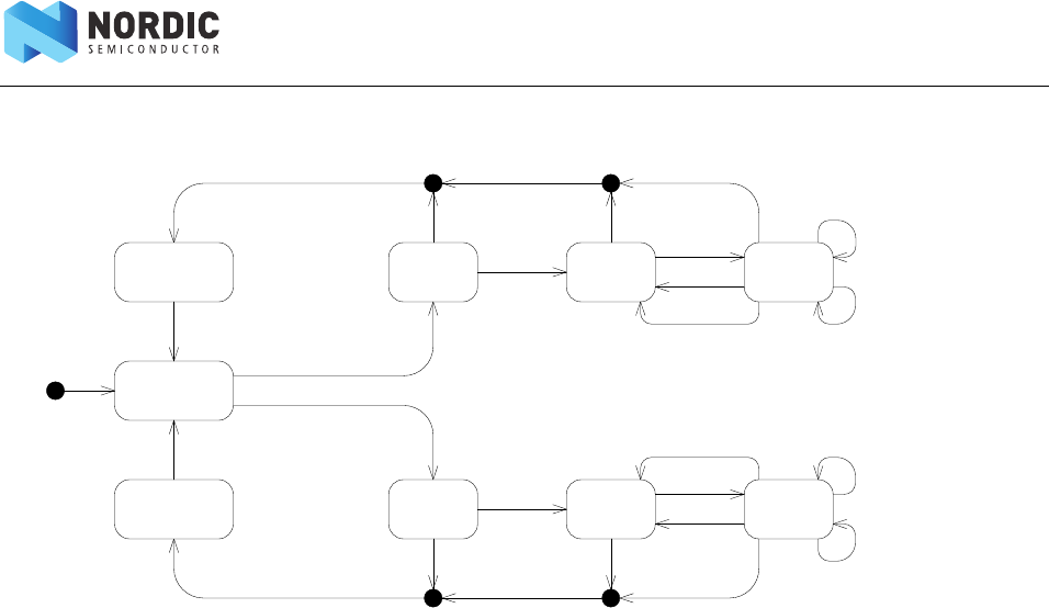
Page 77 of 195
nRF51 Series Reference Manual v2.0 - 2.4 GHz radio (RADIO)
Figure 23 Radio state diagram
16.1.9 Maximum consecutive transmission time
Maximum consecutive transmission time is defined as the longest time the RADIO can be active
transmitting before it has to be disabled, that is, the longest possible time between READY event and
DISABLE task.
Maximum consecutive transmission time for the RADIO is 4 ms running off a 60 ppm crystal and 16 ms
running off a 30 ppm crystal.
DISABLED
TXRU TXIDLE TX
TXEN
Ramp-up
complete
/ READY
START
Packet sent / END
Address sent / ADDRESS
Payload sent [payload length >=0]
/ PAYLOAD
DISABLE
RXRU RXIDLE RX
RXEN
Ramp-up
complete
/ READY
START
Packet received / END Address received [Address match]
/ ADDRESS
Payload received [payload length >=0]
/ PAYLOAD
DISABLE
RXDISABLE
/ DISABLED
TXDISABLE
/ DISABLED
STOP
STOP
Page 78 of 195
nRF51 Series Reference Manual v2.0 - 2.4 GHz radio (RADIO)
16.1.10 Transmit sequence
Before the RADIO is able to transmit a packet, it must first ramp-up in TX mode, see TXRU in Figure 23 on
page 77 and Figure 24. A TXRU ramp-up sequence is initiated when the TXEN task is triggered. After the
radio has successfully ramped up it will generate the READY event indicating that a packet transmission can
be initiated. A packet transmission is initiated by triggering the START task. As illustrated in Figure 23 on
page 77 the START task can first be triggered after the RADIO has entered into the TXIDLE state.
Figure 24 illustrates a single packet transmission where the CPU manually triggers the different tasks
needed to control the flow of the RADIO, that is, no shortcuts are used. If shortcuts are not used, a certain
amount of delay caused by CPU execution is expected between READY and START, and between END and
DISABLE. As illustrated in Figure 23 on page 77 the RADIO will by default transmit '1's between READY and
START and between END and DISABLED.
Figure 24 Transmit sequence
A slightly modified version of the transmit sequence from Figure 24 is illustrated in Figure 25 where the
RADIO is configured to use shortcuts between READY and START, and between END and DISABLE, and
therefore no delay is introduced.
Figure 25 Transmit sequence using shortcuts to avoid delays.
Sta te
TXRU
TX EN
Lifeline
31
END
2
READY
STA RT
P AYL OAD
DISABLE
DIS ABL ED
TXIDLE
Tr a nsm it t er
AS0 LS1 PAYLOAD CRCP
TX TXIDLE TXDISABLE
ADDRESS
’1’’1’
State
TXRU
TX EN
Lifeline
21
END
READY
STA RT
PAYLOAD
DISABLE
DIS ABL ED
Tr a ns m it ter
AS0 LS1 PAYLOAD CRCP
TX TXDISABLE
ADDRESS
’1’
Page 79 of 195
nRF51 Series Reference Manual v2.0 - 2.4 GHz radio (RADIO)
The RADIO is able to send multiple packets one after the other without having to disable and re-enable the
RADIO between packets, this is illustrated in Figure 26.
Figure 26 Transmission of multiple packets
16.1.11 Receive sequence
Before the RADIO is able to receive a packet, it must first ramp-up in RX mode. An RXRU ramp-up sequence
is initiated when the RXEN task is triggered. After the radio has successfully ramped up it will generate the
READY event indicating that a packet reception can be initiated. A packet reception is initiated by triggering
the START task. As illustrated in Figure 27 the START task can first be triggered after the RADIO has entered
into the RXIDLE state.
Figure 28 on page 80 illustrates a single packet reception where the CPU manually triggers the different
tasks needed to control the flow of the RADIO, that is, no shortcuts are used. If shortcuts are not used, a
certain amount of delay, caused by CPU execution, is expected between READY and START, and between
END and DISABLE. As illustrated in Figure 28 on page 80 the RADIO will be listening and possibly receiving
undefined data, illustrated with an 'X', from START and until a packet with valid preamble (P) is received.
Figure 27 Receive sequence
A slightly modified version of the receive sequence from Figure 27 is illustrated in Figure 28 on page 80
where the RADIO is configured to use shortcuts between READY and START, and between END and DISABLE,
and therefore no delay is introduced.
State
TXRU
TX EN
Lifeline
31
END
READY
STA RT
PAYLOAD
DISABLE
DISABLED
Tr a ns m it te r
AS0 LS1 PAYLOAD CRCP
TX TXDISABLE
ADDRESS
END
STA RT
PAYLOAD
AS0 LS1 PAYLOAD CRCP
TX
ADDRESS
2
’1’ ’1’
TXIDLE
State
RXRU
RXEN
Lifeline
31
END
2
READY
STA RT
P AYL OAD
DISABLE
DIS ABL ED
RXIDLE
Reception
AS0 LS1 PAYLOAD CRCP
RX RXIDLE RXDISABLE
ADDRESS
’X’
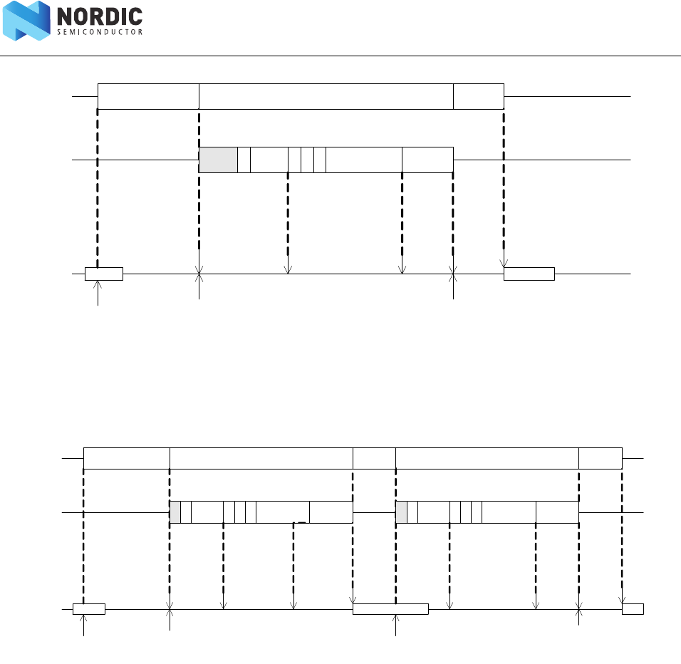
Page 80 of 195
nRF51 Series Reference Manual v2.0 - 2.4 GHz radio (RADIO)
Figure 28 Receive sequence using shortcuts to avoid delays
The RADIO is able to receive multiple packets one after the other without having to disable and re-enable
the RADIO between packets, this is illustrated Figure 29.
Figure 29 Reception of multiple packets
16.1.12 Interframe spacing
Interframe spacing is the time interval between two consecutive packets. It is defined as the time, in micro
seconds, from the end of the last bit of the previous packet received and to the start of the first bit of the
subsequent packet that is transmitted. The RADIO is able to enforce this interval as specified in the TIFS
register as long as TIFS is not specified to be shorter than the RADIO’s startup time (see the radio timing
parameters tTXEN and tRXEN in the product specification for details), that is, the time needed to switch off the
receiver, and switch back on the transmitter. TIFS is only enforced if END_DISABLE and DISABLED_TXEN
shortcuts are enabled. TIFS is only qualified for use in BLE_1MBIT mode.
16.1.13 Device address match
The device address match feature is tailored for address white listing in a Bluetooth low energy and similar
implementations. This feature enables on-the-fly device address matching while receiving a packet on air.
This feature only works in receive mode and as long as RADIO is configured for little endian.
Sta te
RXRU
RXEN
Lifeline
21
END
READY
STA RT
P AYL OAD
DISABLE
DIS ABL ED
Reception
AS0 LS1 PAYLOAD CRCP
RX RXDISABLE
ADDRESS
’X’
State
RXRU
RXEN
Lifeline
31
END
READY
STA RT
PAYLOAD
DISABLE
DISABLED
Receiver
AS0 LS1 PAYLOAD CRCP
RX RXDISABLE
ADDRESS
END
STA RT
PAYLOAD
AS0 LS1 PAYLOAD CRCP
RX
ADDRESS
2
’X’ ’X’
RXIDLE
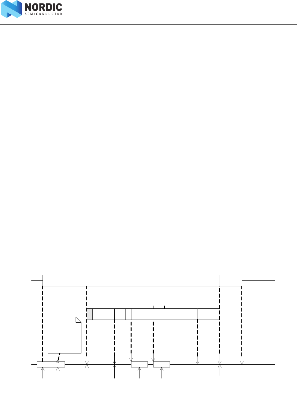
Page 81 of 195
nRF51 Series Reference Manual v2.0 - 2.4 GHz radio (RADIO)
The Device Address match unit assumes that the 48 first bits of the payload is the device address and that bit
number 6 in S0 is the TxAdd bit. See the Bluetooth specification 4.0 for more information about device
addresses, TxAdd, and whitelisting.
The RADIO is able to listen for 8 different device addresses at the same time. These addresses are specified in
a DAB/DAP register pair, one pair per address, in addition to a TxAdd bit configured in the DACNF register.
The DAB register specifies the 32 least significant bits of the device address, while the DAP register specifies
the 16 most significant bits of the device address.
Each of the device addresses can be individually included or excluded from the matching mechanism. This is
configured in the DACNF register.
16.1.14 Bit counter
The RADIO implements a simple counter that can be configured to generate an event after a specific
number of bits have been transmitted or received. By using shortcuts, this counter can be started from
different events generated by the RADIO and then count relative to these events.
The bit counter can only be started after the RADIO has received the ADDRESS event.
The bit counter starts counting after it is started with the BCSTART task, and stopped by triggering the
BCSTOP task. A BCMATCH event will be generated when the bit counter has counted the number of bits
specified in the BCC register. The bit counter will continue to count bits until the DISABLED event is
generated or until the BCSTOP task is triggered. The CPU can therefore, after a BCMATCH event, reconfigure
the BCC value for new BCMATCH events within the same packet.
The bit counter will stop and reset on BCSTOP, STOP, and DISABLE tasks. The bit counter is also stopped and
reset on END event unless the END_START shortcut is enabled.
Figure 30 illustrates how the bit counter can be used to generate a BCMATCH event in the beginning of the
packet payload (BCC=12 bits), and generate a second BCMATCH event after sending 2 bytes (BCC=12 + 16
bits) of the payload.
Figure 30 Bit counter example.
RXEN
Lifeline
1
END
READY
STA RT
PAYLOAD
DISABLE
DIS ABL ED
Reception
AS0 LS1 PAYLOAD CRCP
ADDRESS
BCMATCH
State
RXRU RX RXDISABLE
2
BCSTART
BCC = 12
This exam ple
assumes that the
combined length
of S 0, Length (L)
and S 1 is 12
bits .
BCC = 12 + 16
BCMATCH
3
BCSTOP
012
’X’

Page 82 of 195
nRF51 Series Reference Manual v2.0 - 2.4 GHz radio (RADIO)
16.1.15 Override registers
The OVERRIDE[n] (n=0…4) registers must be configured for a specific radio mode if override parameters
have been written to the FICR during production calibration. It is not possible to partially override these
parameters, meaning all five registers must either be used or left untouched.
16.1.15.1 Using the Override registers
Before enabling the radio, check if the FICR contains override parameters for the selected radio mode by
reading the FICR.OVERRIDDEN register. If the FICR contains override parameters for this mode, they have to
be copied into the RADIO.OVERRIDE[n] (n=0…4) registers before the radio is enabled. See Chapter 6
“Factory Information Configuration Registers (FICR)” on page 18 for further details.
Override can be disabled by setting the value of OVERRIDE[4].OREN to 0. Override can be re-enabled by
setting the value of OVERRIDE[4].OREN to 1.
Configuration of the OVERRIDE registers, including OVERRIDE[4].OREN, must occur before the radio is
enabled using the RXEN or TXEN task. The registers must not be overwritten while the radio is enabled, that
is, from RADIO.RXEN or RADIO.TXEN until the RADIO.DISABLED event.

Page 83 of 195
nRF51 Series Reference Manual v2.0 - 2.4 GHz radio (RADIO)
16.2 Register
Register Offset Description
TASKS
TXEN 0x000 Enable radio in TX mode.
RXEN 0x004 Enable radio in RX mode.
START 0x008 Start radio.
STOP 0x00C Stop radio.
DISABLE 0x010 Disable radio.
RSSISTART 0x014 Task for starting the RSSI and take one single sample of the receive signal
strength.
RSSISTOP 0x018 Task for stopping the RSSI measurement.
BCSTART 0x01C Start bit counter.
BCSTOP 0x020 Stop bit counter.
EVENTS
READY 0x100 Ready event.
ADDRESS 0x104 Address event.
PAYLOAD 0x108 Payload event.
END 0x10C End event.
DISABLED 0x110 Disabled event.
DEVMATCH 0x114 A device address match occurred on the last received packet.
DEVMISS 0x118 No device address match occurred on the last received packet.
RSSIEND 0x11C Sampling of receive signal strength complete. A new RSSI sample is ready for
readout from the RSSISAMPLE register.
BCMATCH 0x128 Bit counter reached bit count value specified in BCC.
REGISTERS
SHORTS 0x200 Shortcuts for the radio.
INTENSET 0x304 Interrupt enable set register.
INTENCLR 0x308 Interrupt enable clear register.
CRCSTATUS 0x400 CRC status.
RXMATCH 0x408 Received address.
RXCRC 0x40C Received CRC.
DAI 0x410 Device address match index.
PACKETPTR 0x504 Packet pointer.
FREQUENCY 0x508 Frequency.
TXPOWER 0x50C Output power.
MODE 0x510 Data rate and modulation.
PCNF0 0x514 Packet configuration 0.
PCNF1 0x518 Packet configuration 1.
BASE0 0x51C Base address 0.
BASE1 0x520 Base address 1.
PREFIX0 0x524 Prefixes bytes for logical addresses 0-3.

Page 84 of 195
nRF51 Series Reference Manual v2.0 - 2.4 GHz radio (RADIO)
Table 19 Register overview
PREFIX1 0x528 Prefixes bytes for logical addresses 4-7.
TXADDRESS 0x52C Transmit address select.
RXADDRESSES 0x530 Receive address select.
CRCCNF 0x534 CRC configuration.
CRCPOLY 0x538 CRC polynomial.
CRCINIT 0x53C CRC initial value.
TEST 0x540 Test features enable register.
TIFS 0x544 Interframe Spacing in µs.
RSSISAMPLE 0x548 RSSI sample.
STATE 0x550 Current radio state.
DATAWHITEIV 0x554 Data whitening initial value.
BCC 0x560 Bit counter compare.
DAB[0] 0x600 Device address 0 base segment.
DAB[1] 0x604 Device address 1 base segment.
.. .. ..
DAB[7] 0x61C Device address 7 base segment.
DAP[0] 0x620 Device address 0 prefix.
DAP[1] 0x624 Device address 1 prefix.
.. .. ..
DAP[7] 0x63C Device address 7 prefix.
DACNF 0x640 Device address match configuration.
.. .. ..
OVERRIDE[0] 0x724 Override0 - Radio configuration parameters.
OVERRIDE[1] 0x728 Override1 - Radio configuration parameters.
OVERRIDE[2] 0x72C Override2 - Radio configuration parameters.
OVERRIDE[3] 0x730 Override3 - Radio configuration parameters.
OVERRIDE[4] 0x734 Override4 - Radio configuration parameters.
.. .. ..
POWER 0xFFC Peripheral power control.
Register Offset Description

Page 85 of 195
nRF51 Series Reference Manual v2.0 - 2.4 GHz radio (RADIO)
16.2.1 SHORTS
16.2.2 CRCSTATUS
16.2.3 RXMATCH
16.2.4 RXCRC
Bit number 31 30 29 28 27 26 25 24 23 22 21 20 19 18 17 16 15 14 13 12 11 10 9 8 7 6 5 4 3 2 1 0
ID (Field ID) - - - - - - - - - - - - - - - - - - - - - - - I - G F E DC B A
Reset value 0 0 0 0 0 0 0 0 0 0 0 0 0 0 0 0 0 0 0 0 0 0 0 0 0 0 0 0 0 0 0 0
ID RW Field Value
ID Value Description
A RW READY_START Enable or disable shortcut between READY event and START task.
BRW END_DISABLE Enable or disable shortcut between END event and DISABLE task.
C RW DISABLED_TXEN Enable or disable shortcut between DISABLED event and TXEN task.
DRW DISABLED_RXEN Enable or disable shortcut between DISABLED event and RXEN task.
E RW ADDRESS_RSSISTART Enable or disable shortcut between ADDRESS event and RSSISTART task.
FRW END_START Enable or disable shortcut between END event and START task.
G RW ADDRESS_BCSTART Enable or disable shortcut between ADDRESS event and BCSTART task.
IRW DISABLED_RSSISTOP Enable or disable shortcut between DISABLED event and RSSISTOP task.
Bit number 31 30 29 28 27 26 25 24 23 22 21 20 19 18 17 16 15 14 13 12 11 10 9 8 7 6 5 4 3 2 1 0
ID (Field ID) - - - - - - - - - - - - - - - - - - - - - - - - - - - - - - - A
Reset value 0 0 0 0 0 0 0 0 0 0 0 0 0 0 0 0 0 0 0 0 0 0 0 0 0 0 0 0 0 0 0 0
ID RW Field Value ID Value Description
A R CRC status of packet received
0Packet received with CRC error
1 Packet received with CRC OK
Bit number 31 30 29 28 27 26 25 24 23 22 21 20 19 18 17 16 15 14 13 12 11 10 9 8 7 6 5 4 3 2 1 0
ID (Field ID) - - - - - - - - - - - - - - - - - - - - - - - - - - - - - A A A
Reset value 0 0 0 0 0 0 0 0 0 0 0 0 0 0 0 0 0 0 0 0 0 0 0 0 0 0 0 0 0 0 0 0
ID RW Field Value ID Value Description
A R Logical address on which previous packet was received.
Bit number 31 30 29 28 27 26 25 24 23 22 21 20 19 18 17 16 15 14 13 12 11 10 9 8 7 6 5 4 3 2 1 0
ID (Field ID) - - - - - - - - A A A A A A A A A A A A A A A A A A A A A A A A
Reset value 00000000000000000000000000000000
ID RW Field Value ID Value Description
A R CRC field of previously received packet.

Page 86 of 195
nRF51 Series Reference Manual v2.0 - 2.4 GHz radio (RADIO)
16.2.5 PACKETPTR
16.2.6 TXPOWER
16.2.7 MODE
Bit number 31 30 29 28 27 26 25 24 23 22 21 20 19 18 17 16 15 14 13 12 11 10 9 8 7 6 5 4 3 2 1 0
ID (Field ID) AAAAAAAAAAAAAAAAAAAAAAAAAAAAAAAA
Reset value 00000000000000000000000000000000
ID RW Field Value ID Value Description
A RW Packet address to be used for the next transmission or reception. When
transmitting, the packet pointed to by this address will be transmitted and
when receiving, the received packet will be written to this address.
This address is a byte aligned RAM address.
Decision point: START task.
Bit number 31 30 29 28 27 26 25 24 23 22 21 20 19 18 17 16 15 14 13 12 11 10 9 8 7 6 5 4 3 2 1 0
ID (Field ID) ------------------------AAAAAAAA
Reset value 00000000000000000000000000000000
ID RW Field Value ID Value Description
A RW Radio output power. Decision point: TXEN task.
POS_4_DBM 0x04 + 4 dBm
0_DBM 0 0 dBm
NEG_4_DBM 0xFC -4 dBm
NEG_8_DBM 0xF8 -8 dBm
NEG_12_DBM 0xF4 -12 dBm
NEG_16_DBM 0xF0 -16 dBm
NEG_20_DBM 0xEC -20 dBm
NEG_30_DBM 0xD8 -30 dBm
Bit number 31 30 29 28 27 26 25 24 23 22 21 20 19 18 17 16 15 14 13 12 11 10 9 8 7 6 5 4 3 2 1 0
ID (Field ID) - - - - - - - - - - - - - - - - - - - - - - - - - - - - - - A A
Reset value 0 0 0 0 0 0 0 0 0 0 0 0 0 0 0 0 0 0 0 0 0 0 0 0 0 0 0 0 0 0 0 0
ID RW Field Value ID Value Description
A RW Radio data rate and modulation setting.
The radio supports Frequency-shift Keying (FSK) modulation, which depending
on setting are compatible with either Nordic Semiconductor’s proprietary
radios, or Bluetooth low energy.
NRF_1MBIT 01 Mbit/s Nordic proprietary radio mode
NRF_2MBIT 1 2 Mbit/s Nordic proprietary radio mode
NRF_250_KBIT 2250 kbit/s Nordic proprietary radio mode
BLE_1MBIT 3 1 Mbit/s Bluetooth Low Energy.

Page 87 of 195
nRF51 Series Reference Manual v2.0 - 2.4 GHz radio (RADIO)
16.2.8 PCNF0
Bit number 31 30 29 28 27 26 25 24 23 22 21 20 19 18 17 16 15 14 13 12 11 10 9 8 7 6 5 4 3 2 1 0
ID (Field ID) - - - - - - - - - - - - C C C C - - - - - - - B - - - - A A A A
Reset value 00000000000000000000000000000000
ID RW Field Value ID Value Description
A RW LFLEN [0..8] Length of length field in number of bits. Decision point: START task.
BRW S0LEN [0..1] Length of S0 field in number of bytes. Decision point: START task.
C RW S1LEN [0..8] Length of S1 field in number of bits. Decision point: START task.

Page 88 of 195
nRF51 Series Reference Manual v2.0 - 2.4 GHz radio (RADIO)
16.2.9 PCNF1
16.2.10 BASE0
16.2.11 BASE1
Bit number 31 30 29 28 27 26 25 24 23 22 21 20 19 18 17 16 15 14 13 12 11 10 9 8 7 6 5 4 3 2 1 0
ID (Field ID) - - - - - - E D - - - - - C C C B B B B B B B B A A A A A A A A
Reset value 00000000000000000000000000000000
ID RW Field Value ID Value Description
A RW MAXLEN [0..255] Maximum length of packet payload. If the payload of a packet is larger than
MAXLEN the radio will only receive MAXLEN number of bytes.
BRW STATLEN [0..255] Static length in number of bytes. The radio will send and receive N bytes more
than what is defined in the Length field of the packet. Usually the RADIO will
send/receive the number of bytes defined by the Length field in the RADIO
packet. If you want to send more than that, you do so by adding a static length
of N bytes to the packet.
Decision point: START task.
C RW BALEN [2..4] Base address length in number of bytes. The address field is composed of the
base address and the one byte long address prefix, e.g. set BALEN=2 to get a
total address of 3 bytes.
Decision point: START task.
DRW ENDIAN On air endianness of packet length field.
Decision point: START task.
LITTLE 0 Least significant bit on air first
BIG 1Most significant bit on air first
E RW WHITEEN Packet whitening enabled
0Disabled
1Enabled
Bit number 31 30 29 28 27 26 25 24 23 22 21 20 19 18 17 16 15 14 13 12 11 10 9 8 7 6 5 4 3 2 1 0
ID (Field ID) A A A A A A A A A A A A A A A A A A A A A A A A A A A A A A A A
Reset value 0 0 0 0 0 0 0 0 0 0 0 0 0 0 0 0 0 0 0 0 0 0 0 0 0 0 0 0 0 0 0 0
ID RW Field Value ID Value Description
A RW Radio base address 0. Decision point: START task.
Bit number 31 30 29 28 27 26 25 24 23 22 21 20 19 18 17 16 15 14 13 12 11 10 9 8 7 6 5 4 3 2 1 0
ID (Field ID) A A A A A A A A A A A A A A A A A A A A A A A A A A A A A A A A
Reset value 0 0 0 0 0 0 0 0 0 0 0 0 0 0 0 0 0 0 0 0 0 0 0 0 0 0 0 0 0 0 0 0
ID RW Field Value ID Value Description
A RW Radio base address 1. Decision point: START task.

Page 89 of 195
nRF51 Series Reference Manual v2.0 - 2.4 GHz radio (RADIO)
16.2.12 PREFIX0
16.2.13 PREFIX1
16.2.14 TXADDRESS
Bit number 31 30 29 28 27 26 25 24 23 22 21 20 19 18 17 16 15 14 13 12 11 10 9 8 7 6 5 4 3 2 1 0
ID (Field ID) D D D D D D D D C C C C C C C C B B B B B B B B A A A A A A A A
Reset value 0 0 0 0 0 0 0 0 0 0 0 0 0 0 0 0 0 0 0 0 0 0 0 0 0 0 0 0 0 0 0 0
ID RW Field Value ID Value Description
A RW AP0 Address prefix 0. Decision point: START task.
BRW AP1 ..
CRW AP2 ..
DRW AP3 ..
Bit number 31 30 29 28 27 26 25 24 23 22 21 20 19 18 17 16 15 14 13 12 11 10 9 8 7 6 5 4 3 2 1 0
ID (Field ID) D D D D D D D D C C C C C C C C B B B B B B B B A A A A A A A A
Reset value 00000000000000000000000000000000
ID RW Field Value ID Value Description
A RW AP4 Address prefix 4. Decision point: START task.
BRW AP5 ..
CRW AP6 ..
DRW AP7 ..
Bit number 31 30 29 28 27 26 25 24 23 22 21 20 19 18 17 16 15 14 13 12 11 10 9 8 7 6 5 4 3 2 1 0
ID (Field ID) - - - - - - - - - - - - - - - - - - - - - - - - - - - - - A A A
Reset value 0 0 0 0 0 0 0 0 0 0 0 0 0 0 0 0 0 0 0 0 0 0 0 0 0 0 0 0 0 0 0 0
ID RW Field Value ID Value Description
A RW Logical address to be used when transmitting a packet. Decision point: START
task.

Page 90 of 195
nRF51 Series Reference Manual v2.0 - 2.4 GHz radio (RADIO)
16.2.15 RXADDRESSES
16.2.16 CRCCNF
16.2.17 CRCPOLY
Bit number 31 30 29 28 27 26 25 24 23 22 21 20 19 18 17 16 15 14 13 12 11 10 9 8 7 6 5 4 3 2 1 0
ID (Field ID) ------------------------HGFEDCBA
Reset value 00000000000000000000000000000000
ID RW Field Value ID Value Description
A RW ADR0 Enable reception on logical address 0. Decision point START task
0Disable
1Enable
BRW ADR1 ..
CRW ADR2 ..
DRW ADR3 ..
ERW ADR4 ..
FRW ADR5 ..
GRW ADR6 ..
HRW ADR7 ..
Bit number 31 30 29 28 27 26 25 24 23 22 21 20 19 18 17 16 15 14 13 12 11 10 9 8 7 6 5 4 3 2 1 0
ID (Field ID) -----------------------B------AA
Reset value 00000000000000000000000000000000
ID RW Field Value ID Value Description
A RW LEN [1..3] CRC length in number of bytes. Decision point: START task.
0CRC length is zero, and CRC calculation is disabled.
B RW SKIP_ADR Leave packet address field out of CRC calculation. Decision point: START task.
0CRC calculation includes address field.
1 CRC calculation does not include address field. The CRC calculation will start at
the first byte after the address.
Bit number 31 30 29 28 27 26 25 24 23 22 21 20 19 18 17 16 15 14 13 12 11 10 9 8 7 6 5 4 3 2 1 0
ID (Field ID) - - - - - - - - A A A A A A A A A A A A A A A A A A A A A A A -
Reset value 00000000000000000000000000000000
ID RW Field Value ID Value Description
ARW CRC polynomial.
Each term in the CRC polynomial is mapped to a bit in this register which index
corresponds to the term’s exponent. The least significant term/bit is hardwired to
1.
The following example is for an 8-bit CRC polynomial:
x8 + x7 + x3 + x2 + 1 = 1 1000 1101
Decision point: START task.

Page 91 of 195
nRF51 Series Reference Manual v2.0 - 2.4 GHz radio (RADIO)
16.2.18 CRCINIT
16.2.19 FREQUENCY
16.2.20 TEST
16.2.21 RSSISAMPLE
Bit number 31 30 29 28 27 26 25 24 23 22 21 20 19 18 17 16 15 14 13 12 11 10 9 8 7 6 5 4 3 2 1 0
ID (Field ID) - - - - - - - - A A A A A A A A A A A A A A A A A A A A A A A A
Reset value 00000000000000000000000000000000
ID RW Field Value ID Value Description
A RW Initial value for CRC calculation. Decision point: START task.
Bit number 31 30 29 28 27 26 25 24 23 22 21 20 19 18 17 16 15 14 13 12 11 10 9 8 7 6 5 4 3 2 1 0
ID (Field ID) - - - - - - - - - - - - - - - - - - - - - - - - - A A A A A A A
Reset value 0 0 0 0 0 0 0 0 0 0 0 0 0 0 0 0 0 0 0 0 0 0 0 0 0 0 0 0 0 0 0 0
ID RW Field Value ID Value Description
A RW Radio channel frequency offset in MHz: RF frequency = 2400 + A (MHz)
Decision point: TXEN or RXEN
Bit number 31 30 29 28 27 26 25 24 23 22 21 20 19 18 17 16 15 14 13 12 11 10 9 8 7 6 5 4 3 2 1 0
ID (Field ID) ------------------------------BA
Reset value 00000000000000000000000000000000
ID RW Field Value
ID Value Description
A RW CONST_CARRIER Constant carrier. Decision point: TXEN task.
0Disable
1Enable
BRW PLL_LOCK PLL lock. Decision point: TXEN or RXEN task.
0Disable
1Enable
Bit number 31 30 29 28 27 26 25 24 23 22 21 20 19 18 17 16 15 14 13 12 11 10 9 8 7 6 5 4 3 2 1 0
ID (Field ID) - - - - - - - - - - - - - - - - - - - - - - - - - A A A A A A A
Reset value 0 0 0 0 0 0 0 0 0 0 0 0 0 0 0 0 0 0 0 0 0 0 0 0 0 0 0 0 0 0 0 0
ID RW Field Value ID Value Description
A RW [0..127] RSSI sample result. The value of this register is read as a positive value while the
actual received signal strength is a negative value. Actual received signal
strength is as follows:
Received signal strength = -A [dBm]

Page 92 of 195
nRF51 Series Reference Manual v2.0 - 2.4 GHz radio (RADIO)
16.2.22 STATE
16.2.23 DATAWHITEIV
16.2.24 DAI
16.2.25 TIFS
Bit number 31 30 29 28 27 26 25 24 23 22 21 20 19 18 17 16 15 14 13 12 11 10 9 8 7 6 5 4 3 2 1 0
ID (Field ID) - - - - - - - - - - - - - - - - - - - - - - - - - - - - A A A A
Reset value 0 0 0 0 0 0 0 0 0 0 0 0 0 0 0 0 0 0 0 0 0 0 0 0 0 0 0 0 0 0 0 0
ID RW Field Value ID Value Description
AR Current radio state.
DISABLED 0Radio is in the DISABLED state.
RXRU 1 Radio is in the RXRU state.
RXIDLE 2Radio is in the RXIDLE state.
RX 3 Radio is in the RX state.
RXDISABLE 4Radio is in the RXDISABLE state.
TXRU 9 Radio is in the TXRU state.
TXIDLE 10 Radio is in the TXIDLE state.
TX 11 Radio is in the TX state.
TXDISABLE 12 Radio is in the TXDISABLE state.
Bit number 31 30 29 28 27 26 25 24 23 22 21 20 19 18 17 16 15 14 13 12 11 10 9 8 7 6 5 4 3 2 1 0
ID (Field ID) - - - - - - - - - - - - - - - - - - - - - - - - - 1 A A A A A A
Reset value 0 0 0 0 0 0 0 0 0 0 0 0 0 0 0 0 0 0 0 0 0 0 0 0 0 1 0 0 0 0 0 0
ID RW Field Value ID Value Description
A RW Data whitening initial value. Bit 0 corresponds to Position 6 of the LSFR, Bit 1 to
Position 5. etc. Decision point: TXEN and RXEN.
Bit number 31 30 29 28 27 26 25 24 23 22 21 20 19 18 17 16 15 14 13 12 11 10 9 8 7 6 5 4 3 2 1 0
ID (Field ID) - - - - - - - - - - - - - - - - - - - - - - - - - - - - - A A A
Reset value 0 0 0 0 0 0 0 0 0 0 0 0 0 0 0 0 0 0 0 0 0 0 0 0 0 1 0 0 0 0 0 0
ID RW Field Value ID Value Description
AR Index(n) of device address, see DAB[n] and DAP[n], that got an address match.
Bit number 31 30 29 28 27 26 25 24 23 22 21 20 19 18 17 16 15 14 13 12 11 10 9 8 7 6 5 4 3 2 1 0
ID (Field ID) - - - - - - - - - - - - - - - - - - - - - - - - A A A A A A A A
Reset value 0 0 0 0 0 0 0 0 0 0 0 0 0 0 0 0 0 0 0 0 0 0 0 0 0 1 0 0 0 0 0 0
ID RW Field Value ID Value Description
A RW Interframe spacing.
Interframe space is the time interval between two consecutive packets. It is
defined as the time, in micro seconds, from the end of the last bit of the previous
packet to the start of the first bit of the subsequent packet.
Decision point: START task.

Page 93 of 195
nRF51 Series Reference Manual v2.0 - 2.4 GHz radio (RADIO)
16.2.26 DAB[n] (n=0..7)
16.2.27 DAP[n] (n=0..7)
Bit number 31 30 29 28 27 26 25 24 23 22 21 20 19 18 17 16 15 14 13 12 11 10 9 8 7 6 5 4 3 2 1 0
ID (Field ID) A A A A A A A A A A A A A A A A A A A A A A A A A A A A A A A A
Reset value 0 0 0 0 0 0 0 0 0 0 0 0 0 0 0 0 0 0 0 0 0 0 0 0 0 1 0 0 0 0 0 0
ID RW Field Value ID Value Description
A RW Device address base segment.
Bit number 31 30 29 28 27 26 25 24 23 22 21 20 19 18 17 16 15 14 13 12 11 10 9 8 7 6 5 4 3 2 1 0
ID (Field ID) - - - - - - - - - - - - - - - - A A A A A A A A A A A A A A A A
Reset value 0 0 0 0 0 0 0 0 0 0 0 0 0 0 0 0 0 0 0 0 0 0 0 0 0 1 0 0 0 0 0 0
ID RW Field Value ID Value Description
A RW Device address prefix.

Page 94 of 195
nRF51 Series Reference Manual v2.0 - 2.4 GHz radio (RADIO)
16.2.28 DACNF
16.2.29 BCC
16.2.30 OVERRIDE[n] (n=0..3)
Bit number 31 30 29 28 27 26 25 24 23 22 21 20 19 18 17 16 15 14 13 12 11 10 9 8 7 6 5 4 3 2 1 0
ID (Field ID) - - - - - - - - - - - - - - - - P O N M L K J I H G F E D C B A
Reset value 0 0 0 0 0 0 0 0 0 0 0 0 0 0 0 0 0 0 0 0 0 0 0 0 0 1 0 0 0 0 0 0
ID RW Field Value ID Value Description
ARW ENA0
0
1
Enable or disable device address matching using device address 0.
Disable
Enable
BRW ENA1 ..
CRW ENA2 ..
DRW ENA3 ..
ERW ENA4 ..
FRW ENA5 ..
GRW ENA6 ..
HRW ENA7 ..
I RW TXADD0 TxAdd for device address 0.
JRW TXADD1 ..
K RW TXADD2 ..
LRW TXADD3 ..
M RW TXADD4 ..
NRW TXADD5 ..
O RW TXADD6 ..
PRW TXADD7 ..
Bit number 31 30 29 28 27 26 25 24 23 22 21 20 19 18 17 16 15 14 13 12 11 10 9 8 7 6 5 4 3 2 1 0
ID (Field ID) A A A A A A A A A A A A A A A A A A A A A A A A A A A A A A A A
Reset value 0 0 0 0 0 0 0 0 0 0 0 0 0 0 0 0 0 0 0 0 0 0 0 0 0 0 0 0 0 0 0 0
ID RW Field Value ID Value Description
A RW Bit counter compare
Bit number 31 30 29 28 27 26 25 24 23 22 21 20 19 18 17 16 15 14 13 12 11 10 9 8 7 6 5 4 3 2 1 0
ID (Field ID) A A A A A A A A A A A A A A A A A A A A A A A A A A A A A A A A
Reset value 0 0 0 0 0 0 0 0 0 0 0 0 0 0 0 0 0 0 0 0 0 0 0 0 0 0 0 0 0 0 0 0
ID RW Field Value ID Value Description
A R Radio override

Page 95 of 195
nRF51 Series Reference Manual v2.0 - 2.4 GHz radio (RADIO)
16.2.31 OVERRIDE[4]
16.2.32 POWER
Bit number 31 30 29 28 27 26 25 24 23 22 21 20 19 18 17 16 15 14 13 12 11 10 9 8 7 6 5 4 3 2 1 0
ID (Field ID) B A A A A A A A A A A A A A A A A A A A A A A A A A A A A A A A
Reset value 0 0 0 0 0 0 0 0 0 0 0 0 0 0 0 0 0 0 0 0 0 0 0 0 0 0 0 0 0 0 0 0
ID RW Field Value ID Value Description
A RW Radio override
BRW OREN
0
1
Override control.
Disable use of OVERRIDE[n] (n=0...4) registers.
Enable use of OVERRIDE[n] (n=0...4) registers.
Bit number 31 30 29 28 27 26 25 24 23 22 21 20 19 18 17 16 15 14 13 12 11 10 9 8 7 6 5 4 3 2 1 0
ID (Field ID) - - - - - - - - - - - - - - - - - - - - - - - - - - - - - - - A
Reset value 0 0 0 0 0 0 0 0 0 0 0 0 0 0 0 0 0 0 0 0 0 0 0 0 0 0 0 0 0 0 0 1
ID RW Field Value ID Value Description
ARW
0
1
Peripheral power control. The peripheral and its registers are reset to its initial
state by switching the peripheral off and then back on again.
Peripheral is powered off
Peripheral is powered on
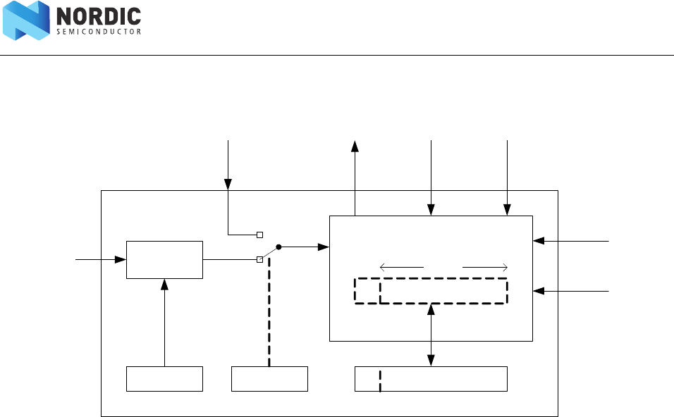
Page 96 of 195
nRF51 Series Reference Manual v2.0 - Timer/counter (TIMER)
17 Timer/counter (TIMER)
Figure 31 Block schematic for Time/counter
17.1 Functional description
The TIMER can operate in two modes, Timer mode and Counter mode. In both modes the TIMER is started
by triggering the START task, and stopped by triggering the STOP task. The TIMER is a count-up timer.
In Timer mode, the TIMER's internal Counter register is incremented by one for every tick of the timer
frequency fTIMER as illustrated in Figure 31. The timer frequency is derived from HFCLK as described below
using the values specified in the PRESCALER register:
In counter mode, the TIMER's internal Counter register is incremented by one each time the COUNT task is
triggered, that is, the timer frequency and the prescaler are not utilized in counter mode. Similarly, the
COUNT task has no effect in Timer mode.
The TIMER's maximum value is configured by changing the bit-width of the timer in the BITMODE register.
For details on which bit-widths that are supported on the different timers see the device product
specification.
The PRESCALER register and the BITMODE register must only be updated when the timer is stopped. If these
registers are updated while the TIMER is started then this may result in unpredictable behavior.
When the timer is incremented beyond its maximum value the Counter register will overflow and the TIMER
will automatically start over from zero.
The Counter register can be cleared, that is, its internal value set to zero explicitly, by triggering the CLEAR
task.
TIMER
HFCLK Prescaler
TIMER Core
CC[0..n]
COMPARE [0 ..n] CAPTURE[0..n]COUNT
f
TIMER
In c r e m e n t
MODEPRESCALER
START
STOP
CLEAR
Counter
BITMODE
fTIMER
HFCLK
2PRESCALER
-----------------------------
=

Page 97 of 195
nRF51 Series Reference Manual v2.0 - Timer/counter (TIMER)
The TIMER implements multiple capture/compare registers, see the product specification for more
information on how many capture/compare registers that are supported in the chip.
17.1.1 Compare
The TIMER implements one COMPARE event for every available capture/compare register. A COMPARE event
is generated when the Counter is incremented and then becomes equal to the value specified in one of the
capture compare registers. When the Counter value becomes equal to the value specified in a capture
compare register CC[n], the corresponding compare event COMPARE[n] is generated.
BITMODE specifies how many bits of the Counter register and the capture/compare register that are used
when the comparison is performed. Other bits will be ignored.
17.1.2 Capture
The TIMER implements one capture task for every available capture/compare register. Every time the
CAPTURE[n] task is triggered the Counter value is copied to the CC[n] register.
17.1.3 Task priority
If the START task and the STOP task are triggered at the same time, that is, within the same period of HFCLK,
the STOP task will be prioritized.
17.1.4 Task delays
The CLEAR task, COUNT task and the STOP task will guarantee to take effect within one clock cycle of the
HFCLK. Depending on sub-power mode, the START task may require longer time to take effect, see product
specification for more information. See POWER chapter, Chapter 11 “Power management (POWER)” on
page 40, for more information about sub-power modes.

Page 98 of 195
nRF51 Series Reference Manual v2.0 - Timer/counter (TIMER)
17.2 Registers
Table 20 Register overview
Register Offset Description
TASKS
START 0x000 Start Timer
STOP 0x004 Stop Timer
COUNT 0x008 Increment Timer (Counter mode only)
CLEAR 0x00C Clear timer
CAPTURE[0] 0x040 Capture Timer value to CC0 register
CAPTURE[1] 0x044 Capture Timer value to CC1 register
CAPTURE[2] 0x048 Capture Timer value to CC2 register
CAPTURE[3] 0x04C Capture Timer value to CC3 register
EVENTS
COMPARE[0] 0x140 Compare event on CC[0] match
COMPARE[1] 0x144 Compare event on CC[1] match
COMPARE[2] 0x148 Compare event on CC[2] match
COMPARE[3] 0x14C Compare event on CC[3] match
REGISTERS
SHORTS 0x200 Shortcuts
INTENSET 0x304 Interrupt enable set register
INTENCLR 0x308 Interrupt enable clear register
MODE 0x504 Timer mode selection
BITMODE 0x508 Configure the number of bits used by the TIMER
PRESCALER 0x510 Timer prescaler register
CC[0] 0x540 Capture/Compare register 0
CC[1] 0x544 Capture/Compare register 1
CC[2] 0x548 Capture/Compare register 2
CC[3] 0x54C Capture/Compare register 3

Page 99 of 195
nRF51 Series Reference Manual v2.0 - Timer/counter (TIMER)
17.2.1 SHORTS
17.2.2 MODE
17.2.3 PRESCALER
Bit number 31 30 29 28 27 26 25 24 23 22 21 20 19 18 17 16 15 14 13 12 11 10 9 8 7 6 5 4 3 2 1 0
ID (Field ID) - - - - - - - - - - - - - - - - - - - - H G F E - - - - D C B A
Reset value 0 0 0 0 0 0 0 0 0 0 0 0 0 0 0 0 0 0 0 0 0 0 0 0 0 0 0 0 0 0 0 0
ID Field Value Description
A RW COMPARE0_CLEAR Enable or disable shortcut between COMPARE0 and CLEAR task.
BRW COMPARE1_ CLEAR Enable or disable shortcut between COMPARE1 and CLEAR task.
C RW COMPARE2_ CLEAR Enable or disable shortcut between COMPARE2 and CLEAR task.
DRW COMPARE3_ CLEAR Enable or disable shortcut between COMPARE3 and CLEAR task.
E RW COMPARE0 _STOP Enable or disable shortcut between COMPARE0 and STOP task.
FRW COMPARE 1_STOP Enable or disable shortcut between COMPARE1 and STOP task.
G RW COMPARE2_STOP Enable or disable shortcut between COMPARE2 and STOP task.
HRW COMPARE3_STOP Enable or disable shortcut between COMPARE3 and STOP task.
Bit number 31 30 29 28 27 26 25 24 23 22 21 20 19 18 17 16 15 14 13 12 11 10 987654321 0
ID (Field ID) - - ----------------------------- A
Reset value 0000000000000000000000000000000 0
ID RW Field Value Description
ARW Timer mode
TIMER 0Select timer mode
COUNTER 1 Select counter mode
Bit number 31 30 29 28 27 26 25 24 23 22 21 20 19 18 17 16 15 14 13 12 11 10 9 8 7 6 5 4 3 2 1 0
ID (Field ID) - - --------------------------AAA A
Reset value 0000000000000000000000000000010 0
ID RW Field Value Description
ARW [0..9] Prescaler value

Page 100 of 195
nRF51 Series Reference Manual v2.0 - Timer/counter (TIMER)
17.2.4 BITMODE
Bit number 31 30 29 28 27 26 25 24 23 22 21 20 19 18 17 16 15 14 13 12 11 10 9 8 7 6 5 4 3 2 1 0
ID (Field ID) - - - - - - - - - - - - - - - - - - - - - - - - - - - - - - A A
Reset value 0 0 0 0 0 0 0 0 0 0 0 0 0 0 0 0 0 0 0 0 0 0 0 0 0 0 0 0 0 0 0 0
ID RW Field Value Description
ARW Timer bit width
16BIT 016 bit timer bit width
08BIT 1 8 bit timer bit width
24BIT 224 bit timer bit width
32BIT 3 32 bit timer bit width
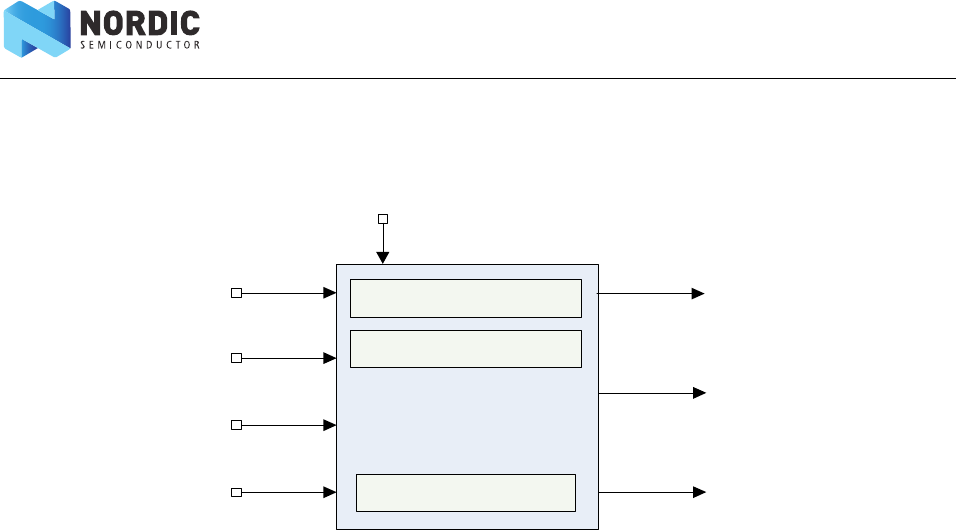
Page 101 of 195
nRF51 Series Reference Manual v2.0 - Real Time Counter (RTC)
18 Real Time Counter (RTC)
Figure 32 RTC block schematic
18.1 Functional description
The RTC is a 24 bit low-frequency clock with frequency prescaling and tick, compare, and overflow events.
18.1.1 Clock Source
The RTC will run off a low-frequency clock (LFCLK) running at 32.768 kHz. This clock may be either a RC
oscillator or a crystal oscillator. The COUNTER resolution will therefore be 30.517 µs. The RTC must be able to
run while the 16 MHz system clock (SysClk) source is OFF.
18.1.2 Resolution versus overflow and the PRESCALER
COUNTER increment frequency:
The PRESCALER register is read/write when the RTC is stopped. The PRESCALER register is read-only once
the RTC is STARTed. Writing to the PRESCALER register when the RTC is started has no effect.
The PRESCALER is restarted on START, CLEAR and TRIGOVRFLW, that is, the prescaler value is latched to an
internal register (<<PRESC>>) on these tasks.
RTC
32.768 kHz
CC[0:3]
PRESCALER
COUNTER
task
CLEAR
task
TRIGOVRFLW
event TICK
event OVRFLW
event COMPARE[0..N]
task
START
task
STOP
fRTC
32 768kHz
PRESCALER 1+
--------------------------------------------
=
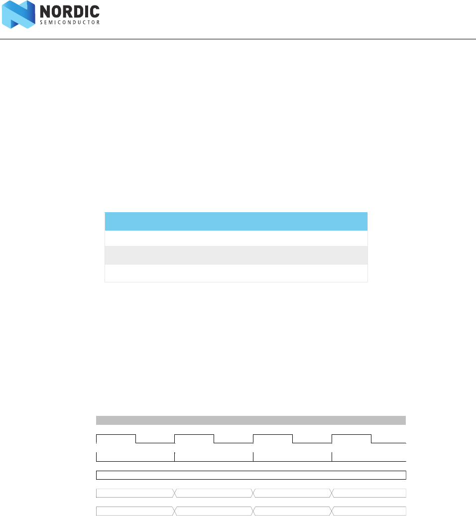
Page 102 of 195
nRF51 Series Reference Manual v2.0 - Real Time Counter (RTC)
Examples
1. Desired COUNTER frequency 100 Hz (10 ms per counter period)
PRESCALER = round(32.768 kHz / 100 Hz) - 1 = 327
fRTC = 99.9 Hz
10009.576 s counter period
2. Desired COUNTER frequency 8 Hz (125 millisecond counter period)
PRESCALER = round (32.768 kHz / 8 Hz) – 1 = 4095
fRTC = 8 Hz
125 ms counter period
Table 21 RTC Resolution versus Overflow
18.1.3 The COUNTER register
The COUNTER increments on LFCLK when the internal PRESCALER register (<<PRESC>>) is 0x00. The
internal <<PRESC>> register is reloaded from the PRESCALER register. If enabled, the TICK event occurs on
each increment of the COUNTER. The TICK event can be disabled.
Figure 33 Timing diagram - COUNTER_PRESCALER_0
Prescaler Counter resolution Overflow
0 30.517 µs 512 seconds
28 - 1 7812.5 µs 131072 seconds
212 - 1 125 ms 582.542 hours
0x000
0x000 0x000 0x000 0x000
0x000000 0x000001 0x000002 0x000003
Sy sClk
LFClk
TICK
PRESC
<<PRESC>>
COUNTER

Page 103 of 195
nRF51 Series Reference Manual v2.0 - Real Time Counter (RTC)
Figure 34 Timing diagram - COUNTER_PRESCALER_1
18.1.4 Overflow features
The TRIGOVRFLW task sets the COUNTER value to 0xFFFFF0 to allow SW test of the overflow condition.
OVRFLW occurs when COUNTER overflows from 0xFFFFFF to 0x000000.
Note: The OVRFLW event is disabled by default.
18.1.5 The TICK event
The TICK event enables low power “tick-less” RTOS implementation as it optionally provides a regular
interrupt source for a RTOS without the need to use the ARM® SysTick feature. Using the RTC TICK event
rather than the SysTick allows the CPU to be powered down while still keeping RTOS scheduling active.
Note: The TICK event is disabled by default.
18.1.6 Event Control feature
To optimize RTC power consumption, events in the RTC can be prevented from being routed to the PPI by
configuring the EVTEN register. When routing an event to the PPI is disabled the HFCLK will no longer be
required and power consumption will be reduced.
For example, if the TICK event is not required for an application, routing of this event to the PPI should be
disabled as it is frequently occurring and may raise power consumption if HFCLK can otherwise be powered
down for long durations.
18.1.7 Compare feature
There are three supported compare registers and up to one optional. See product specification for details on
available compare registers.
When setting a compare register, the following behavior of the RTC compare event should be noted:
• If a CC register value is 0 when a CLEAR task is set, this will not trigger a COMPARE event.
0x001
0x000 0x001 0x000 0x001
0x000000
0x000001
Sy sClk
LFClk
TICK
PRESC
<<PRESC>>
COUNTER
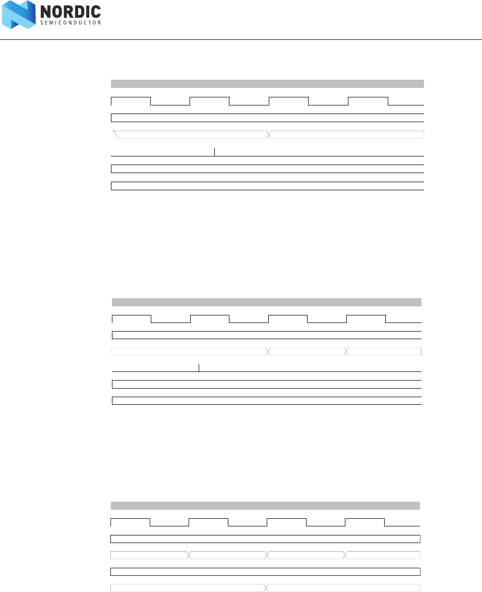
Page 104 of 195
nRF51 Series Reference Manual v2.0 - Real Time Counter (RTC)
Figure 35 Timing diagram –COMPARE_CLEAR
• If a CC register is N and the COUNTER value is N when the START task is set, this will not
trigger a COMPARE event.
Figure 36 Timing diagram - COMPARE_START
• COMPARE occurs when a CC register is N and the COUNTER value transitions from N-1 to N.
Figure 37 Timing diagram - COMPARE
• If the COUNTER is N, writing N+2 to a CC register is guaranteed to trigger a COMPARE event
at N+2.
0x000
X
0x000000
0x000000
0
Sy sClk
LFClk
PRESC
COUNTER
CLEAR
CC[0]
COMPARE[0]
0x000
N-1 N
N+1
N
0
Sy sClk
LFClk
PRESC
COUNTER
START
CC[0]
COMPARE[0]
0x000
N-2 N-1
N
N+1
N
0 1
Sy sClk
LFClk
PRESC
COUNTER
CC[0]
COMPARE[0]
Page 105 of 195
nRF51 Series Reference Manual v2.0 - Real Time Counter (RTC)
Figure 38 Timing diagram - COMPARE_N+2
• If the COUNTER is N, writing N or N+1 to a CC register may not trigger a COMPARE event.
Figure 39 Timing diagram - COMPARE_N+1
• If the COUNTER is N and the current CC register value is N+1 or N+2 when a new CC value is
written, a match may trigger on the previous CC value before the new value takes effect. If
the current CC value greater than N+2 when the new value is written, there will be no event
due to the old value.
Figure 40 Timing diagram - COMPARE_N-1
0x000
N-1 N
N+1
N+2
X
N+2
0
1
> 62.5ns
Sy sClk
LFClk
PRESC
COUNTER
CC[0]
COMPARE[0]
0x000
N-2 N-1
NN+1
X
N+1
0
>= 0
Sy sClk
LFClk
PRESC
COUNTER
CC[0]
COMPARE[0]
0x000
N-2 N-1 N
N+1
N+1
X
0 1
>= 0
Sy sClk
LFClk
PRESC
COUNTER
CC[0]
COMPARE[0]

Page 106 of 195
nRF51 Series Reference Manual v2.0 - Real Time Counter (RTC)
18.1.8 TASK and EVENT jitter/delay
The source of jitter or delay in the RTC is due to the peripheral clock being a low frequency clock (LFCLK)
which is not synchronous to the faster system clock (SysClk). Registers in the peripheral interface, part of the
SysClk domain, have a set of mirrored registers in the LFCLK domain. For example, the COUNTER value
accessible from the CPU is in the SysClk domain and is latched on read from an internal register called
COUNTER in the LFCLK domain. COUNTER is the register which is actually modified each time the RTC ticks.
These registers must be synchronised between clock domains (SysClk and LFCLK).
The following is a summary of the jitter introduced on tasks and events. Figures illustrating jitter follow.
Table 22 RTC jitter magnitudes on tasks
Table 23 RTC jitter magnitudes on events
1. CLEAR and STOP (and TRIGOVRFLW; not shown) will be delayed as long as it takes for the
peripheral to clock a falling edge and rising of the LFCLK. This is between 15.2585 µs and 45.7755
µs – rounded to 15 µs and 46 µs for the remainder of the section.
Figure 41 Timing diagram - DELAY_CLEAR
Task Delay
CLEAR, STOP, START, TRIGOVRFLW +15 to 46 s
Operation/Function Jitter
START to COUNTER increment +/- 15 s
COMPARE to COMPARE1
1.Assumes RTC runs continuously between these events.
Note: 32.768 kHz clock jitter is additional to the above provided numbers
+/- 62.5 ns
0x000
X
X+1 0x000000 0x000001
CLEAR
1 or more Sy sClk bef ore
0 or more Sy sClk af ter
>= ~15us
<= ~46us
Sy sClk
LFClk
PRESC
COUNTER
CLEARa
CLEARb
Page 107 of 195
nRF51 Series Reference Manual v2.0 - Real Time Counter (RTC)
Figure 42 Timing diagram - DELAY_STOP
2. The START task will start the RTC. The first increment of COUNTER (and instance of TICK event) will
be after 30. 5 µs +/-15 µs, again because at least 1 falling edge must occur after the START TASK
before the rising edge causes events and COUNTER increment. The figures show the smallest and
largest delays to on the START task which appears as a +/-15 µs jitter on the first COUNTER
increment.
Figure 43 Timing diagram - JITTER_START–
0x000
X
X+1
STOP
1 or more Sy sClk bef ore
0 or more Sy sClk af ter
>= ~15us
<= ~46us
Sy sClk
LFClk
PRESC
COUNTER
STOPa
STOPb
0x000
X
X+1 X+2
X+3
START
0 or more Sy sClk bef ore
>= ~15us
Sy sClk
LFClk
PRESC
COUNTER
START
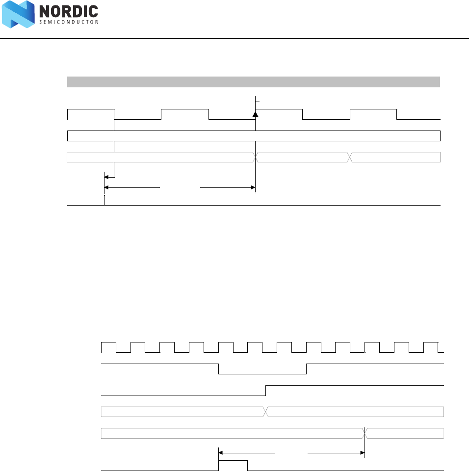
Page 108 of 195
nRF51 Series Reference Manual v2.0 - Real Time Counter (RTC)
Figure 44 Timing diagram - JITTER_START+
18.1.9 Reading the COUNTER register
To read the COUNTER register, the internal <<COUNTER>> value is sampled. To ensure <<COUNTER>> is
safely sampled (considering a LFCLK transition may occur during a read), the CPU and core memory bus are
halted for 3 cycles by lowering the core PREADY signal. The Read takes the CPU 2 cycles in addition resulting
in the COUNTER register read taking a fixed five SysClk clock cycles.
Figure 45 Timing diagram - COUNTER_READ
0x000
X
X+1
X+2
START
0 or more Sy sClk bef ore
<= ~45us
Sy sClk
LFClk
PRESC
COUNTER
START
N-1
N
X
N
375.2ns
Sy sClk
PREADY
LFClk
<<COUN TER>>
COUNTER
COUNTER_READ

Page 109 of 195
nRF51 Series Reference Manual v2.0 - Real Time Counter (RTC)
18.2 Registers
Register Offset Description
TASKS
START 0x000 Start RTC COUNTER.
STOP 0x004 Stop RTC COUNTER.
CLEAR 0x008 Clear RTC COUNTER.
TRIGOVRFLW 0x00C Set COUNTER to 0xFFFFF0.
EVENTS
TICK 0x100 Event on COUNTER increment.
OVRFLW 0x104 Event on COUNTER overflow.
COMPARE[0] 0x140 Compare event on CC[0] match.
COMPARE[1] 0x144 Compare event on CC[1] match.
COMPARE[2] 0x148 Compare event on CC[2] match.
COMPARE[3] 0x14C Compare event on CC[3] match.
REGISTERS
INTENSET 0x304 Configures which events shall generate a RTC interrupt.
INTENCLR 0x308 Configures which events shall not generate a RTC interrupt.
EVTEN 0x340 Enable or disable event routing to PPI.
EVTENSET 0x344 Enable event routing to PPI.
EVTENCLR 0x348 Disable event routing to PPI.
COUNTER 0x504 Current COUNTER value.
PRESCALER 0x508 12 bit prescaler for COUNTER frequency (32768/(PRESCALER+1)).
Must be written when RTC is stopped.
CC[0] 0x540 Compare register.
CC[1] 0x544 Compare register.
CC[2] 0x548 Compare register.
CC[3] 0x54C Compare register.

Page 110 of 195
nRF51 Series Reference Manual v2.0 - Real Time Counter (RTC)
18.2.1 EVTEN
Bit number 31 30 29 28 27 26 25 24 23 22 21 20 19 18 17 16 15 14 13 12 11 10 9 8 7 6 5 4 3 2 1 0
ID (Field ID) - - - - - - - - - - - - F E D C - - - - - - - - - - - - - - B A
Reset value 0 0 0 0 0 0 0 0 0 0 0 0 0 0 0 0 0 0 0 0 0 0 0 0 0 0 0 0 0 0 0 0
ID RW Field Value ID Value Description
A RW TICK Enable or disable routing of TICK event to PPI.
1Enable
0Disable
BRW OVERFLW Enable or disable routing of OVRFLW event to PPI.
1Enable
0Disable
C RW COMPARE0 Enable or disable routing of COMPARE[0]event to PPI.
1Enable
0Disable
DRW COMPARE1 Enable or disable routing of COMPARE[1]event to PPI.
1Enable
0Disable
E RW COMPARE2 Enable or disable routing of COMPARE[2]event to PPI.
1Enable
0Disable
FRW COMPARE3 Enable or disable routing of COMPARE[3]event to PPI.
1Enable
0Disable

Page 111 of 195
nRF51 Series Reference Manual v2.0 - Real Time Counter (RTC)
18.2.2 EVTENSET
Bit number 31 30 29 28 27 26 25 24 23 22 21 20 19 18 17 16 15 14 13 12 11 10 9 8 7 6 5 4 3 2 1 0
ID (Field ID) - - - - - - - - - - - - F E D C - - - - - - - - - - - - - - B A
Reset value 0 0 0 0 0 0 0 0 0 0 0 0 0 0 0 0 0 0 0 0 0 0 0 0 0 0 0 0 0 0 0 0
ID RW Field Value ID Value Description
A TICK Enable routing of TICK event to PPI.
W 1 Enable
R EVTEN.0 Readback bit 0 of EVTEN
BOVRFLW Enable routing of OVRFLW event to PPI.
W1Enable
REVTEN.1 Readback bit 1 of EVTEN
C COMPARE0 Enable routing of COMPARE[0] event to PPI.
W 1 Enable
R EVTEN.16 Readback bit 16 of EVTEN
DCOMPARE1 Enable routing of COMPARE[1] event to PPI.
W1Enable
REVTEN.17 Readback bit 17 of EVTEN
E COMPARE2 Enable routing of COMPARE[2] event to PPI.
W 1 Enable
R EVTEN.18 Readback bit 18 of EVTEN
FCOMPARE3 Enable routing of COMPARE[3] event to PPI.
W1Enable
REVTEN.19 Readback bit 19 of EVTEN

Page 112 of 195
nRF51 Series Reference Manual v2.0 - Real Time Counter (RTC)
18.2.3 EVTENCLR
18.2.4 COUNTER
18.2.5 PRESCALER
Bit number 31 30 29 28 27 26 25 24 23 22 21 20 19 18 17 16 15 14 13 12 11 10 9 8 7 6 5 4 3 2 1 0
ID (Field ID) - - - - - - - - - - - - F E D C - - - - - - - - - - - - - - B A
Reset value 0 0 0 0 0 0 0 0 0 0 0 0 0 0 0 0 0 0 0 0 0 0 0 0 0 0 0 0 0 0 0 0
ID RW Field Value ID Value Description
A TICK Disable routing of TICK event to PPI.
W 1 Disable
R EVTEN.0 Readback bit 0 of EVTEN
BOVRFLW Disable routing of OVRFLW event to PPI.
W1Disable
REVTEN.1 Readback bit 1 of EVTEN
C COMPARE0 Disable routing of COMPARE[0] event to PPI.
W 1 Disable
R EVTEN.16 Readback bit 16 of EVTEN
DCOMPARE1 Disable routing of COMPARE[1] event to PPI.
W1Disable
REVTEN.17 Readback bit 17 of EVTEN
E COMPARE2 Disable routing of COMPARE[2] event to PPI.
W 1 Disable
R EVTEN.18 Readback bit 18 of EVTEN
FCOMPARE3 Disable routing of COMPARE[3] event to PPI.
W1Disable
REVTEN.19 Readback bit 19 of EVTEN
Bit number 31 30 29 28 27 26 25 24 23 22 21 20 19 18 17 16 15 14 13 12 11 10 9876543210
ID (Field ID) - - - - - - - - A A A A A A A A A A A A A A A A A A A A A A A A
Reset value 00000000000000000000000000000000
ID RW Field Value ID Value Description
ACounter value
Bit number 31 30 29 28 27 26 25 24 23 22 21 20 19 18 17 16 15 14 13 12 11 10 9876543210
ID (Field ID) --------------------AAAAAAAAAAAA
Reset value 00000000000000000000000000000000
ID RW Field Value ID Value Description
APRESCALER value

Page 113 of 195
nRF51 Series Reference Manual v2.0 - Real Time Counter (RTC)
18.2.6 CC[N] (n=0..3)
Bit number 31 30 29 28 27 26 25 24 23 22 21 20 19 18 17 16 15 14 13 12 11 10 9 8 7 6 5 4 3 2 1 0
ID (Field ID) - - - - - - - - A A A A A A A A A A A A A A A A A A A A A A A A
Reset value 0 0 0 0 0 0 0 0 0 0 0 0 0 0 0 0 0 0 0 0 0 0 0 0 0 0 0 0 0 0 0 0
ID RW Field Value ID Value Description
ACompare value

Page 114 of 195
nRF51 Series Reference Manual v2.0 - Watchdog timer (WDT)
19 Watchdog timer (WDT)
19.1 Functional description
The watchdog is implemented as a down-counter that generates a TIMEOUT event when it wraps over after
counting down to 0. The watchdog timer is started by triggering the START task, whereupon the watchdog
counter is loaded with the value specified in the CRV register. This counter is also reloaded with the value
specified in the CRV register when a reload request is granted.
The counter reload value is specified in the CRV register, and the timer is started using the START task.
The watchdog’s timeout period is given by:
When started, the watchdog will automatically force the 32.768 kHz RC oscillator on.
19.1.1 Reload criteria
The watchdog has 8 separate reload request registers which shall be used to request the watchdog to reload
its counter with the value specified in the CRV register. To reload the watchdog counter, the special value
0x6E524635 needs to be written to all enabled reload registers. One or more RR registers can be individually
enabled via the RREN register.
19.1.2 Temporarily pausing the watchdog
By default the watchdog will be active counting down the down-counter while the CPU is sleeping and
when it is halted by the debugger. It is however possible to configure the watchdog to automatically pause
while the CPU is sleeping as well as when it is halted by the debugger.
19.1.3 Watchdog reset
A TIMEOUT event will automatically lead to a watchdog reset equivalent to a system reset, see Chapter 11
“Power management (POWER)” on page 40. If the watchdog is configured to generate an interrupt on the
TIMEOUT event, the watchdog reset will be postponed with two 32.768 kHz clock cycles after the TIMEOUT
event has been generated. Once the TIMEOUT event has been generated, the impending watchdog reset
will always be effectuated.
The watchdog must be configured before it is started. After it is started, the watchdog’s configuration
registers, which comprises registers CRV, RREN, and CONFIG, will be blocked for further configuration.
The watchdog is reset when the device is put into System OFF mode. The watchdog is also reset when the
whole system is reset, except for when the system is reset through a soft reset, see Chapter 11 “Power
management (POWER)” on page 40 for more information about reset types.
When the device starts running again, after a reset, or waking up from OFF mode, the watchdog
configuration registers will be available for configuration again.
CRV 1+
32768
--------------------- s

Page 115 of 195
nRF51 Series Reference Manual v2.0 - Watchdog timer (WDT)
19.2 Registers
Table 24 Register overview
19.2.1 RUNSTATUS
Register Offset Description
TASKS
START 0x000 Start the watchdog
EVENTS
TIMEOUT 0x100 Watchdog timeout
REGISTERS
INTENSET 0x304 Interrupt enable set register
INTENCLR 0x308 Interrupt enable clear register
RUNSTATUS 0x400 Run status
REQSTATUS 0x404 Request status
CRV 0x504 Counter reload value
RREN 0x508 Reload request enable
CONFIG 0x50C Configuration register
RR[0] 0x600 Reload request 0
RR[1] 0x604 Reload request 1
.. .. ..
RR[7] 0x61C Reload request 7
Bit number 31 30 29 28 27 26 25 24 23 22 21 20 19 18 17 16 15 14 13 12 11 10 9 8 7 6 5 4 3 2 1 0
ID (Field ID) - - - - - - - - - - - - - - - - - - - - - - - - - - - - - - - A
Reset value 0 0 0 0 0 0 0 0 0 0 0 0 0 0 0 0 0 0 0 0 0 0 0 0 0 0 0 0 0 0 0 0
ID RW Field Value ID Value Description
AR
0
1
Indicates if the watchdog is running.
Watchdog is not running.
Watchdog is running.

Page 116 of 195
nRF51 Series Reference Manual v2.0 - Watchdog timer (WDT)
19.2.2 REQSTATUS
19.2.3 CRV
19.2.4 RREN
Bit number 31 30 29 28 27 26 25 24 23 22 21 20 19 18 17 16 15 14 13 12 11 10 9 8 7 6 5 4 3 2 1 0
ID (Field ID) -------- ----------------HGFEDCBA
Reset value 00000000 000000000000000000000001
ID RW Field Value ID Value Description
A R RR0 Request status for RR[0] register
0RR[0] register is not enabled, or are already requesting reload
1 RR[0] register is enabled, and are not yet requesting reload
B R RR1 .. ..
C R RR2 .. ..
D R RR3 .. ..
R R RR4 .. ..
F R RR5 .. ..
G R RR6 .. ..
H R RR7 .. ..
Bit number 31 30 29 28 27 26 25 24 23 22 21 20 19 18 17 16 15 14 13 12 11 10 9 8 7 6 5 4 3 2 1 0
ID (Field ID) A A A A A A A A A A A A A A A A A A A A A A A A A A A A A A A A
Reset value 0 0 0 0 0 0 0 0 0 0 0 0 0 0 0 0 0 0 0 0 0 0 0 0 0 0 0 0 0 0 0 0
ID RW Field Value ID Value Description
A RW Counter reload value in number of cycles of the 32.768 kHz clock
Bit number 31 30 29 28 27 26 25 24 23 22 21 20 19 18 17 16 15 14 13 12 11 10 9 8 7 6 5 4 3 2 1 0
ID (Field ID) --------------- ---------HGFEDCBA
Reset value 000000000000000 00000000000000001
ID RW Field Value ID Value Description
A RW RR0 Enable or disable RR[0] register
0Disable RR[0] register
1 Enable RR[0] register
BRW RR1 .. ..
C RW RR2 .. ..
DRW RR3 .. ..
R RW RR4 .. ..
FRW RR5 .. ..
G RW RR6 .. ..
HRW RR7 .. ..

Page 117 of 195
nRF51 Series Reference Manual v2.0 - Watchdog timer (WDT)
19.2.5 CONFIG
19.2.6 RR[n] (n=0..7)
Bit number 31 30 29 28 27 26 25 24 23 22 21 20 19 18 17 16 15 14 13 12 11 10 9 8 7 6 5 4 3 2 1 0
ID (Field ID) - - - - - - - - - - - - - - - - - - - - - - - - - - - - B - - A
Reset value 0 0 0 0 0 0 0 0 0 0 0 0 0 0 0 0 0 0 0 0 0 0 0 0 0 0 0 0 0 0 0 1
ID RW Field Value ID Value Description
A RW SLEEP Configure the watchdog to either be paused, or kept running, while the CPU is
sleeping.
PAUSE 0Pause watchdog while the CPU is sleeping.
RUN 1 Keep the watchdog running while the CPU is sleeping.
BRW HALT Configure the watchdog to either be paused, or kept running, while the CPU is
halted by the debugger.
PAUSE 0 Pause watchdog while the CPU is halted by the debugger.
RUN 1Keep the watchdog running while the CPU is halted by the debugger.
Bit number 31 30 29 28 27 26 25 24 23 22 21 20 19 18 17 16 15 14 13 12 11 10 9 8 7 6 5 4 3 2 1 0
ID (Field ID) A A A A A A A A A A A A A A A A A A A A A A A A A A A A A A A A
Reset value 0 0 0 0 0 0 0 0 0 0 0 0 0 0 0 0 0 0 0 0 0 0 0 0 0 0 0 0 0 0 0 0
ID RW Field Value ID Value Description
A W Reload request register

Page 118 of 195
nRF51 Series Reference Manual v2.0 - Random Number Generator (RNG)
20 Random Number Generator (RNG)
Figure 46 Random Number Generator
20.1 Functional description
The Random Number Generator (RNG) generates true non-deterministic random numbers based on
internal thermal noise.
The RNG is started by triggering the START task. When started, new random numbers are generated
continuously and written to the VALUE register when ready. A VALRDY event is generated for every new
random number that is written to the VALUE register.
20.1.1 Digital error correction
A digital corrector algorithm is employed on the internal bit stream to remove any bias toward ‘1’ or ‘0’. The
bits are then queued into an 8 bit register for parallel readout from the VALUE register.
It is possible to disable the bias in the CONFIG register. This offers a substantial speed advantage, but may
result in a statistical distribution that is not perfectly uniform.
20.1.2 Speed
The time needed to generate one random byte of data is unpredictable, and may vary from one byte to the
next. This is especially true when digital error correction is enabled.
Random Number
Generator
START
STOP
VALRDY
VALUE

Page 119 of 195
nRF51 Series Reference Manual v2.0 - Random Number Generator (RNG)
20.2 Registers
Table 25 Register overview
20.2.1 SHORTS
20.2.2 VALUE
Register Offset Description
TASKS
START 0x000 Task starting the random number generator.
STOP 0x004 Task stopping the random number generator.
EVENTS
VALRDY 0x100 Event being generated for every new random number written to the VALUE register.
REGISTERS
SHORTS 0x200 Shortcut register.
INTENSET 0x304 Interrupt enable set register.
INTENCLR 0x308 Interrupt enable clear register.
CONFIG 0x504 Configuration register.
VALUE 0x508 Output random number.
Bit number 31 30 29 28 27 26 25 24 23 22 21 20 19 18 17 16 15 14 13 12 11 10 9 8 7 6 5 4 3 2 1 0
ID (Field ID) -------------------------------A
Reset value 00000000000000000000000000000000
ID RW Field Value
ID Value Description
A RW VALRDY_STOP Shortcut between VALRDY event and STOP task.
0Disable
1Enable
Bit number 31 30 29 28 27 26 25 24 23 22 21 20 19 18 17 16 15 14 13 12 11 10 9 8 7 6 5 4 3 2 1 0
ID (Field ID) - - - - - - - - - - - - - - - - - - - - - - - - A A A A A A A A
Reset value 0 0 0 0 0 0 0 0 0 0 0 0 0 0 0 0 0 0 0 0 0 0 0 0 0 0 0 0 0 0 0 0
ID RW Field Value ID Value Description
A R [0..255] Generated random number.

Page 120 of 195
nRF51 Series Reference Manual v2.0 - Random Number Generator (RNG)
20.2.3 CONFIG
Bit number 31 30 29 28 27 26 25 24 23 22 21 20 19 18 17 16 15 14 13 12 11 10 9 8 7 6 5 4 3 2 1 0
ID (Field ID) -------------------------------A
Reset value 00000000000000000000000000000000
ID RW Field Value ID Value Description
A RW DERCEN Digital error correction
0Disabled
1Enabled

Page 121 of 195
nRF51 Series Reference Manual v2.0 - Temperature sensor (TEMP)
21 Temperature sensor (TEMP)
21.1 Functional description
The temperature sensor measures the silicon die temperature.
The TEMP is started by triggering the START task. When the temperature measurement is completed, a
DATARDY event will be generated and the result of the measurement can be read from the TEMP register.
When the temperature measurement is completed, the TEMP analog electronics power down to save
power.
The TEMP only supports one-shot operation, meaning that every TEMP measurement has to be explicitly
started using the START task.
21.2 Registers
Table 26 Register overview
21.2.1 TEMP
Register Offset Description
TASKS
START 0x000 Start temperature measurement.
STOP 0x004 Stop temperature measurement.
EVENTS
DATARDY 0x100 Temperature measurement complete, data ready.
REGISTERS
INTENSET 0x304 Interrupt enable set register.
INTENCLR 0x308 Interrupt enable clear register.
TEMP 0x508 Temperature.
Bit number 31 30 29 28 27 26 25 24 23 22 21 20 19 18 17 16 15 14 13 12 11 10 9 8 7 6 5 4 3 2 1 0
R AAAAAAAAAAAAAAAAAAAAAAAAAAAAAAA A
Reset value 0000000000000000000000000000000 0
ID Field Value Description
A Result of temperature measurement. Die temperature in °C, 2’s complement format, 0.25 °C
precision.
Decision point: DATARDY.

Page 122 of 195
nRF51 Series Reference Manual v2.0 - AES Electronic Codebook Mode Encryption (ECB)
22 AES Electronic Codebook Mode Encryption (ECB)
22.1 Functional description
AES ECB is a single AES block encrypt hardware module.
AES ECB features:
• 128 bit AES encryption
• Supports standard AES ECB block encryption
• Memory pointer support
• DMA data transfer
AES ECB performs a 128 bit AES block encrypt. At the STARTECB task, data and key is loaded into the
algorithm by EasyDMA. When output data has been written back to memory, the ENDECB event is triggered.
AES ECB can be stopped by triggering the STOPECB task.
22.1.1 EasyDMA
The ECB implements an EasyDMA mechanism for reading and writing to and from the RAM. When the
ENDECB or ERRORECB is generated EasyDMA stops accessing the RAM.
22.1.2 ECB Data Structure
Input to the block encrypt and output from the block encrypt are stored in the same data structure.
ECBDATAPTR should point to this data structure before STARTECB is initiated.
Table 27 ECB data structure overview
22.1.3 Shared resources
The ECB, CCM, and AAR share the same AES module. The ECB will always have lowest priority and if there is a
sharing conflict during encryption, the ECB operation will be aborted and an ERRORECB event will be
generated.
Property Address
offset Description
KEY 0 16 byte AES key
CLEARTEXT 16 16 byte AES cleartext input block
CIPHERTEXT 32 16 byte AES ciphertext output block

Page 123 of 195
nRF51 Series Reference Manual v2.0 - AES Electronic Codebook Mode Encryption (ECB)
22.2 Registers
Table 28 Register overview
22.2.1 ECBDATAPTR
Register Offset Description
TASKS
STARTECB 0x000 Start ECB block encrypt. If a crypto operation is already running in the AES core, the
STARTECB task will not start a new encryption and an ERRORECB event will be
triggered.
STOPECB 0x004 Abort a possible executing ECB operation. If a running ECB operation is aborted by
STOPECB, the ERRORECB event is triggered.
EVENTS
ENDECB 0x100 ECB block encrypt complete.
ERRORECB 0x104 ECB block encrypt aborted because of a STOPECB task or due to an error.
REGISTERS
INTENSET 0x304 Interrupt enable set register.
INTENCLR 0x308 Interrupt enable clear register.
ECBDATAPTR 0x504 ECB block encrypt memory pointers.
Bit number 31 30 29 28 27 26 25 24 23 22 21 20 19 18 17 16 15 14 13 12 11 10 9 8 7 6 5 4 3 2 1 0
ID (Field ID) A A A A A A A A A A A A A A A A A A A A A A A A A A A A A A A A
Reset value 0 0 0 0 0 0 0 0 0 0 0 0 0 0 0 0 0 0 0 0 0 0 0 0 0 0 0 0 0 0 0 0
ID RW Field Value ID Value Description
A Pointer to the ECB data structure (see Table 27 on page 122)
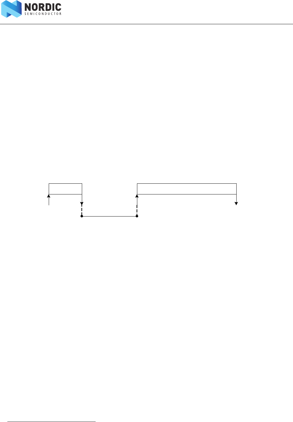
Page 124 of 195
nRF51 Series Reference Manual v2.0 - AES CCM Mode Encryption (CCM)
23 AES CCM Mode Encryption (CCM)
23.1 Functional description
The AES CCM supports three operations: key-stream generation, packet encryption, and packet decryption.
All these operations are done in compliance with the Bluetooth specification1. A new key-stream must be
generated before a new packet encryption or packet decryption operation can be started.
A key-stream is generated by triggering the KSGEN task. An ENDKSGEN event will be generated when the
new key-stream has been generated. The key-stream will be stored in the AES CCM’s temporary memory
area, specified by the SCRATCHPTR, where it will be used in subsequent encryption and decryption
operations.
Encryption is started by triggering the CRYPT task with the MODE register set to ENCRYPTION. Similarly,
decryption is started by triggering the same task with MODE set to DECRYPTION. An ENDCRYPT event will
be generated when packet encryption is completed as well as when packet decryption is completed, see
Figure 47.
Figure 47 Key-stream generation followed by encryption or decryption. The shortcut is optional.
Key-stream generation, packet encryption, and packet decryption operations utilize the configuration
specified in the data structure pointed to by the CNFPTR pointer. It is necessary to configure this pointer and
its underlying data structure, and the MODE register before the KSGEN task is triggered. It is also necessary
to configure the INPTR pointer and the OUTPTR pointer before the CRYPT task is triggered.
If a shortcut is used between ENDKSGEN event and CRYPT task, the INPTR pointer and the OUTPTR pointer
must be configured before the KSGEN task is triggered.
23.1.1 Encryption
During packet encryption the AES CCM will read the unencrypted packet located in RAM at the address
specified in the INPTR pointer, encrypt the packet and append a four byte long Message Integrity Check
(MIC) field to the packet. The AES CCM will also modify the length field of the packet to adjust for the
appended MIC field, that is, add four bytes to the length, and store the resulting packet back into RAM at the
address specified in the OUTPTR pointer, see Figure 48 on page 125.
Empty packets (length field is set to 0) will not be encrypted but instead moved unmodified through the
AES CCM.
The AES CCM is limited to read maximum 27 bytes of the unencrypted payload (PL) regardless of what is
specified in the length field of the unencrypted packet.
1. Bluetooth AES CCM 128 bit block encryption, see Bluetooth specification Version 4.0.
key-stream
generation
KSGEN
encryption / decrypt ion
CRYPTENDKSGEN ENDCRYPT
SHORTCUT
Page 125 of 195
nRF51 Series Reference Manual v2.0 - AES CCM Mode Encryption (CCM)
Figure 48 Encryption
23.1.2 Decryption
During packet decryption the AES CCM will read the encrypted packet located in RAM at the address
specified in the INPTR pointer, decrypt the packet, authenticate the packet’s MIC field and generate the
appropriate MIC status. The AES CCM will also modify the length field of the packet to adjust for the MIC
field, that is, subtract four bytes from the length, and then store the decrypted packet back into RAM at the
address pointed to by the OUTPTR pointer, see Figure 49.
The CCM is only able to decrypt packets that are at least 5 bytes long, that is, 1 byte encrypted payload (EPL)
and 4 bytes of MIC. The CCM will therefore generate a MIC error for packets where the length field is set to 1,
2, 3 or 4.
Empty packets (length field is set to 0) will not be decrypted but instead moved unmodified through the
AES CCM, these packets will always pass the MIC check.
The AES CCM is limited to read maximum 27 bytes of the encrypted payload and four bytes of the MIC
regardless of what is specified in the length field of the encrypted packet.
Figure 49 Decryption
AES CCM
HPLLRFU
HEPLL+4 RFU
Unencr ypted packet
Encrypted packet
MIC
Scratch ar ea
CCM data
structure
MODE = ENCRYPTION
H: Header (S0 )
L: Length
RFU: reserved for future use (S1)
PL: unencr ypted payload
EPL : encr ypted payload
INPTR
OUTPTR
SCRATCHPTR
CNFPTR
AES CCM
HPLLRFU
HEPLL+4 RFU
Unencr ypted packet
Encrypted packet
MIC
Scratch ar ea
CCM data
structure
MODE = DECRYPTION
H: Header (S0 )
L: Length
RFU: reserved for future use (S1)
PL: unencr ypted payload
EPL : encr ypted payload
OUTPTR
INPTR
SCRATCHPTR
CNFPTR
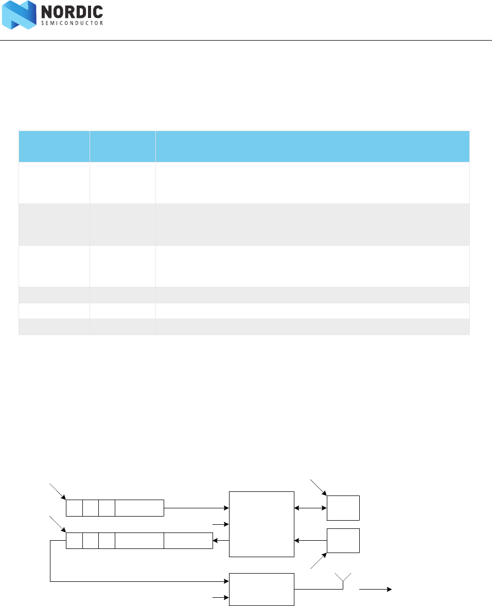
Page 126 of 195
nRF51 Series Reference Manual v2.0 - AES CCM Mode Encryption (CCM)
23.1.3 AES CCM and RADIO concurrent operation
The AES CCM is designed to run in parallel with the RADIO to enable on-the-fly encryption and decryption
of RADIO packets without CPU involvement. To facilitate this, the RADIO has to be configured with the
following settings:
Table 29 Radio configuration settings
23.1.4 Encrypting packets on-the-fly in radio transmit mode
When the AES CCM is encrypting a packet on-the-fly at the same time as the RADIO is transmitting it, the
RADIO must read the encrypted packet from the same memory location as the AES CCM is writing to. The
OUTPTR pointer in the AES CCM must therefore point to the same memory location as the PACKETPTR
pointer in the RADIO, see Figure 50.
Figure 50 Configuration of on-the-fly encryption
In order to match the RADIO’s timing, the KSGEN task must be triggered no later than when the START task
in the RADIO is triggered, in addition the shortcut between the ENDKSGEN event and the CRYPT task must
be enabled. This use-case is illustrated in Figure 51 on page 127 using a PPI connection between the READY
event in the RADIO and the KSGEN task in the AES CCM.
Radio
parameter Value Description
PCNF0.S0LEN 1 S0 field = 1 byte. Must match with the HEADER property in the data structure
associated with INPTR and OUTPTR, see Table 31 on page 129 and Table 32 on
page 129
PCNF0.LFLEN 5Length field = 5 bit. Must match with the LENGTH property in the data structure
associated with INPTR and OUTPTR, see Table 31 on page 129 and Table 32 on
page 129
PCNF0.S1LEN 3 S1 field = 3 bit. Must match with the RFU property in the data structure
associated with INPTR and OUTPTR, see Table 31 on page 129 and Table 32 on
page 129
MODE 1_MBIT_QPSK 1 Mbps data rate
PCNF1.BALEN 3 Length of address (32 bit)
CRCCNF.LEN 3Length of CRC (24 bit)
AES CCM
HPLLRFU
HEPLL+4 RFU
Unencr ypted packet
Encrypted packet
MIC
Scratch ar ea
CCM data
structure
MODE = ENCRYPTION
RADIO
TXEN
To remote
receiver
H: Header (S0 )
L: Length
RFU: reserved for future use (S1)
PL: unencr ypted payload
EPL : encr ypted payload
INPTR
OUTPTR
&
PACKETPTR
SCRATCHPTR
CNFPTR
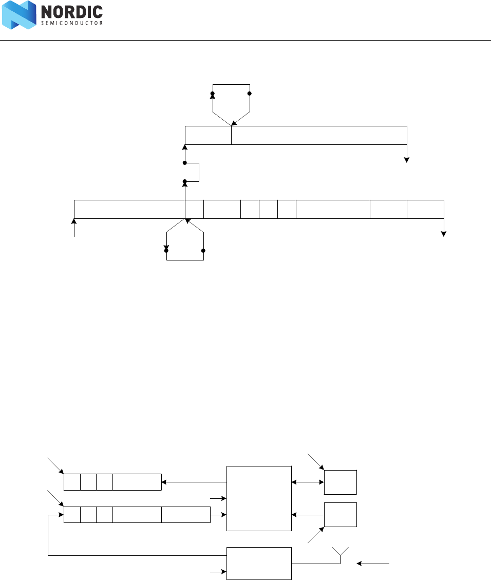
Page 127 of 195
nRF51 Series Reference Manual v2.0 - AES CCM Mode Encryption (CCM)
Figure 51 On-the-fly encryption using a PPI connection
23.1.5 Decrypting packets on-the-fly in radio receive mode
When the AES CCM is decrypting a packet on-the-fly at the same time as the RADIO is receiving it, the AES
CCM must read the encrypted packet from the same memory location as the RADIO is writing to. The INPTR
pointer in the AES CCM must therefore point to the same memory location as the PACKETPTR pointer in the
RADIO, see Figure 52.
Figure 52 Configuration of on-the-fly decryption
In order to match the RADIO’s timing, the KSGEN task must be triggered no later than when the START task
in the RADIO is triggered. In addition, the CRYPT task must be triggered no earlier than when the ADDRESS
event is generated by the RADIO.
If the CRYPT task is triggered exactly at the same time as the ADDRESS event is generated by the RADIO, the
AES CCM will guarantee that the decryption is completed no later than when the END event in the RADIO is
generated.
RU P A H L RFU EPL MI C CRC
READY
TXEN END
key-stream
generation
KSGEN
encryption
ENDCRYPT
READY START
SHORTCUT
RADI O
AES CCM
RU: Ramp-u p of RADI O
P: Preamble
A: Address
H: Header (S0)
L: Length
RFU: reserved for future use (S1)
EPL: encrypted payload
CRYPTENDKSGEN
SHORTCUT
PPI
AES CCM
HPLLRFU
HEPLL+4 RFU
Unencr ypted packet
Encrypted packet
MIC
Scratch ar ea
CCM data
structure
MODE = DECRYPTION
RADIO
RXEN
From remote
transmitter
H: Header (S0 )
L: Length
RFU: reserved for future use (S1)
PL: unencr ypted payload
EPL : encr ypted payload
OUTPTR
INPTR
&
PACKETPTR
SCRATCHPTR
CNFPTR
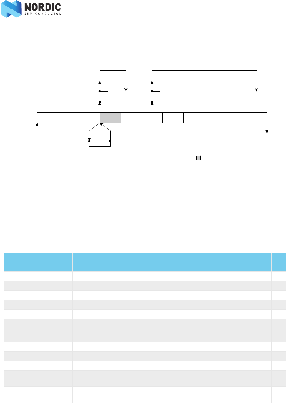
Page 128 of 195
nRF51 Series Reference Manual v2.0 - AES CCM Mode Encryption (CCM)
This use-case is illustrated in Figure 53 using a PPI connection between the ADDRESS event in the RADIO
and the CRYPT task in the AES CCM. The KSGEN task is trigger from the READY event in the RADIO through a
PPI connection.
Figure 53 On-the-fly decryption using a PPI connection between the READY event in the RADIO and the KSGEN
task in the AES CCM
23.1.6 CCM data structure
The CCM data structure specified in Table 30 is located in RAM at the memory location specified by the
CNFPTR pointer register.
Table 30 CCM data structure overview
Property Address
offset Description
KEY 0 16 byte AES key
PKTCTR 16 Octet0 (LSO) of packet counter
17 Octet1 of packet counter
18 Octet2 of packet counter
19 Octet3 of packet counter
20 Bit 6 – Bit 0: Octet4 (7 most significant bits of packet counter, with Bit 6 being the most
significant bit)
Bit7: Ignored
21 Ignored
22 Ignored
23 Ignored
DIRECTION 24 Bit 0: Direction bit
Bit 7 – Bit 1: Zero padded
IV 25 8 byte initialization vector (IV)
Octet0 (LSO) of IV, Octet1 of IV, … , Octet7 (MSO) of IV
RU A H L RFU EPL MI C CRC
ADDRESS
RXEN END
key-stream
generation
KSGEN
decryption
CRYPT
PPI
ENDKSGEN ENDCRYPT
P
READY START
SHORTCUT
RADIO
AES CCM
RU: Ramp-up of RADIO
P: Preamble
A: Address
H: Header (S0)
L: Length
RFU: reserved for future use (S1)
EPL: encrypted payload
: RADIO receiving noise
READY
PPI

Page 129 of 195
nRF51 Series Reference Manual v2.0 - AES CCM Mode Encryption (CCM)
The NONCE vector (as specified by the Bluetooth Core Specification) will be generated by hardware based on
the information specified in the CNFPTR data structure.
Table 31 Data structure for unencrypted packet
Table 32 Data structure for encrypted packet
23.1.7 EasyDMA and ERROR event
The CCM implements an EasyDMA mechanism for reading and writing to the RAM.
In some scenarios where the CPU and other DMA enabled peripherals are accessing the RAM at the same
time, the CCM DMA could experience some bus conflicts which may also result in an error during
encryption. If this happens, the ERROR event will be generated.
EasyDMA finishes accessing the RAM when the ENDKSGEN and ENDCRYPT events are generated.
23.1.8 Shared resources
The CCM shares registers and other resources with other peripherals that have the same ID as the CCM. The
user must therefore disable all peripherals that have the same ID as the CCM before the CCM can be
configured and used. Disabling a peripheral that have the same ID as the CCM will not reset any of the
registers that are shared with the CCM. It is therefore important to configure all relevant CCM registers
explicitly to secure that it operates correctly.
The Instantiation table, Table 3 on page 13, shows which peripherals have the same ID as the CCM.
Property Address offset Description
HEADER 0 Packet Header
LENGTH 1Number of bytes in unencrypted payload
RFU 2 Reserved Future Use
PAYLOAD 30 to 27 bytes unencrypted payload
Property Address offset Description
HEADER 0 Packet Header
LENGTH 1Number of bytes in encrypted payload including length of MIC
Note: LENGTH will be 0 for empty packets since the MIC is not added to empty
packets
RFU 2 Reserved Future Use
PAYLOAD 30 to 27 bytes encrypted payload
MIC 3 + payload
length
ENCRYPT: 4 bytes encrypted MIC
Note: MIC is not added to empty packets

Page 130 of 195
nRF51 Series Reference Manual v2.0 - AES CCM Mode Encryption (CCM)
23.2 Registers
23.2.1 SHORTS
23.2.2 MICSTATUS
Register Offset Description
TASKS
KSGEN 0x000 Start generation of key-stream. This operation will stop by itself when completed.
CRYPT 0x004 Start encryption/decryption. This operation will stop by itself when completed.
STOP 0x008 Stop encryption/decryption
EVENTS
ENDKSGEN 0x100 Key-stream generation complete
ENDCRYPT 0x104 Encrypt/decrypt complete
ERROR 0x108 CCM error event
REGISTERS
SHORTS 0x200 Shortcut register
INTENSET 0x304 Interrupt enable set register
INTENCLR 0x308 Interrupt enable clear register
MICSTATUS 0x400 MIC check result
ENABLE 0x500 Enable
MODE 0x504 Operation mode
CNFPTR 0x508 Pointer to data structure holding AES key and NONCE vector
INPTR 0x50C Input pointer
OUTPTR 0x510 Output pointer
SCRATCHPTR 0x521 Pointer to data area used for temporary storage
Bit number 31 30 29 28 27 26 25 24 23 22 21 20 19 18 17 16 15 14 13 12 11 10 9 8 7 6 5 4 3 2 1 0
ID (Field ID) -------------------------------A
Reset value 00000000000000000000000000000000
ID RW Field Value
ID Value Description
A RW ENDKSGEN_
CRYPT 0
1
Short-cut between ENDKSGEN event and CRYPT task
Disable
Enable
Bit number 31 30 29 28 27 26 25 24 23 22 21 20 19 18 17 16 15 14 13 12 11 10 9 8 7 6 5 4 3 2 1 0
ID (Field ID) -------------------------------A
Reset value 00000000000000000000000000000000
ID RW Field Value
ID Value Description
AR
0
1
The result of the MIC check performed during the previous decryption
operation.
MIC check failed
MIC check passed

Page 131 of 195
nRF51 Series Reference Manual v2.0 - AES CCM Mode Encryption (CCM)
23.2.3 ENABLE
23.2.4 MODE
23.2.5 CNFPTR
23.2.6 INPTR
23.2.7 OUTPTR
Bit number 31 30 29 28 27 26 25 24 23 22 21 20 19 18 17 16 15 14 13 12 11 10 9 8 7 6 5 4 3 2 1 0
ID (Field ID) ------------------------------AA
Reset value 00000000000000000000000000000000
ID RW Field Value
ID Value Description
AR
0
2
Enable CCM
Disable CCM
Enable CCM
Bit number 31 30 29 28 27 26 25 24 23 22 21 20 19 18 17 16 15 14 13 12 11 10 9 8 7 6 5 4 3 2 1 0
ID (Field ID) - - - - - - - - - - - - - - - - - - - - - - - - - - - - - - - A
Reset value 0 0 0 0 0 0 0 0 0 0 0 0 0 0 0 0 0 0 0 0 0 0 0 0 0 0 0 0 0 0 0 1
ID RW Field Value ID Value Description
ARW
Encryption
Decryption
0
1
The mode operation to be used.
AES CCM packet encryption mode
AES CCM packet decryption mode
Bit number 31 30 29 28 27 26 25 24 23 22 21 20 19 18 17 16 15 14 13 12 11 10 9 8 7 6 5 4 3 2 1 0
ID (Field ID) A A A A A A A A A A A A A A A A A A A A A A A A A A A A A A A A
Reset value 0 0 0 0 0 0 0 0 0 0 0 0 0 0 0 0 0 0 0 0 0 0 0 0 0 0 0 0 0 0 0 0
ID RW Field Value ID Value Description
A RW Pointer to the data structure holding the AES key and the CCM NONCE vector
(see Table 30 on page 128 on CCM data structure overview)
Bit number 31 30 29 28 27 26 25 24 23 22 21 20 19 18 17 16 15 14 13 12 11 10 9 8 7 6 5 4 3 2 1 0
ID (Field ID) A A A A A A A A A A A A A A A A A A A A A A A A A A A A A A A A
Reset value 0 0 0 0 0 0 0 0 0 0 0 0 0 0 0 0 0 0 0 0 0 0 0 0 0 0 0 0 0 0 0 0
ID RW Field Value ID Value Description
ARW Input pointer
Bit number 31 30 29 28 27 26 25 24 23 22 21 20 19 18 17 16 15 14 13 12 11 10 9 8 7 6 5 4 3 2 1 0
ID (Field ID) A A A A A A A A A A A A A A A A A A A A A A A A A A A A A A A A
Reset value 0 0 0 0 0 0 0 0 0 0 0 0 0 0 0 0 0 0 0 0 0 0 0 0 0 0 0 0 0 0 0 0
ID RW Field Value ID Value Description
A RW Output pointer

Page 132 of 195
nRF51 Series Reference Manual v2.0 - AES CCM Mode Encryption (CCM)
23.2.8 SCRATCHPTR
Bit number 31 30 29 28 27 26 25 24 23 22 21 20 19 18 17 16 15 14 13 12 11 10 9 8 7 6 5 4 3 2 1 0
ID (Field ID) A A A A A A A A A A A A A A A A A A A A A A A A A A A A A A A A
Reset value 0 0 0 0 0 0 0 0 0 0 0 0 0 0 0 0 0 0 0 0 0 0 0 0 0 0 0 0 0 0 0 0
ID RW Field Value ID Value Description
A Pointer to a ‘scratch’ data area used for temporary storage during key-stream
generation, MIC generation and encryption/decryption.
The scratch area is used for temporary storage of data during key-stream
generation and encryption. A space of minimum 43 bytes must be reserved.
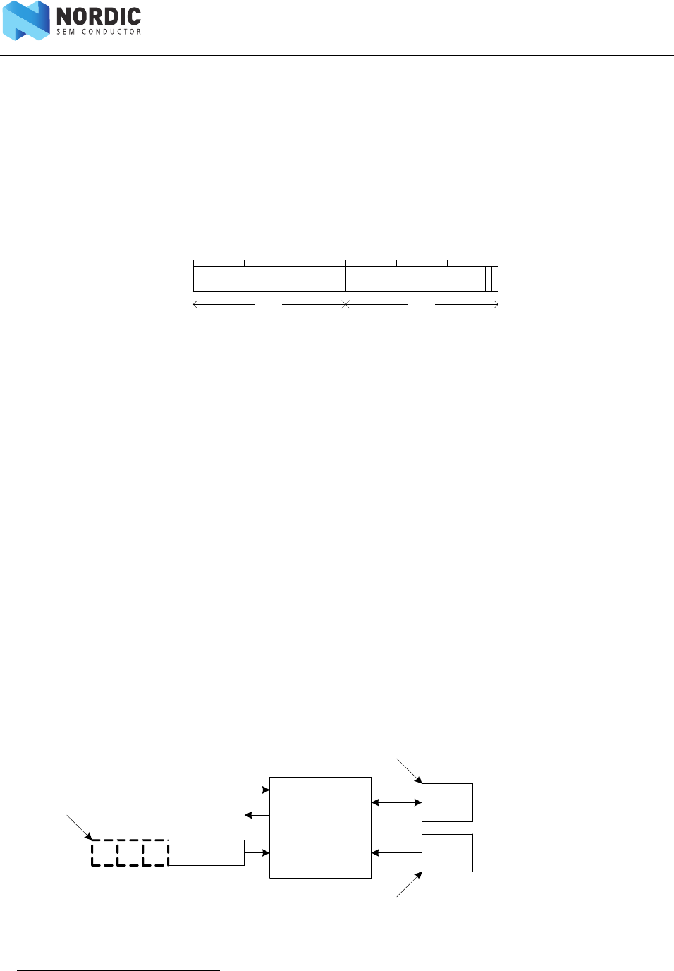
Page 133 of 195
nRF51 Series Reference Manual v2.0 - Accelerated Address Resolver (AAR)
24 Accelerated Address Resolver (AAR)
24.1 Functional description
24.1.1 Resolving a resolvable address
A private resolvable address shall be composed of 6 bytes as illustrated in Figure 54.
Figure 54 Resolvable address
To resolve an address the ADDRPTR pointer must point to the least significant byte (LSB) of the resolvable
address offset by 3 bytes to accommodate the packet header. The resolver is started by triggering the START
task. A RESOLVED event is generated when and if the AAR manages to resolve the address using one of the
Identity Resolving Keys (IRK) found in the IRK data structure. The AAR will use the IRK specified in the register
IRK0 to IRK15 starting from IRK0. How many to be used is specified by the NIRK register. The AAR module will
generate a NOTRESOLVED event if it is not able to resolve the address using the specified list of IRKs.
The AAR will go through the list of available IRKs in the IRK data structure and for each IRK try to resolve the
address according to the Resolvable Private Address Resolution Procedure described in the Bluetooth
Specification2. The time it takes to resolve an address may vary depending on where in the list the
resolvable address is located. The resolution time will also be affected by RAM accesses performed by other
peripherals and the CPU. See product specification for more information about resolution time.
The AAR will not distinguish between public and random addresses. The AAR will also not distinguish
between static and private addresses, or between private resolvable and private non-resolvable addresses.
The AAR will stop as soon as it has managed to resolve the address, or after trying to resolve the address
using NIRK number of IRKs from the IRK data structure. The AAR will generate an END event after it has
stopped.
Figure 55 Address resolution with packet preloaded into RAM
2. Bluetooth Specification Version 4.0 [Vol 3] chapter 10.8.2.3.
r andom
LSB MSB
10
hash
(24-bit)
prand
(24-bit)
AAR
ADDR
Scr atch area
IRK data
structure
ADDR: resolvable addr ess
ADDRPTR
SCRATCHPTR
IRKPTR
S1LS0
RESOLVED
START
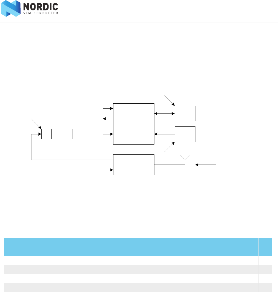
Page 134 of 195
nRF51 Series Reference Manual v2.0 - Accelerated Address Resolver (AAR)
24.1.2 Use case example for chaining RADIO packet reception with resolving addresses
with the AAR
The AAR may be started as soon as the 6 bytes required by the AAR has been received by the RADIO and
stored in RAM. The ADDRPTR pointer must point to the least significant byte of the resolvable address within
the received packet.
Figure 56 Address resolution with packet loaded into RAM by the RADIO
24.1.3 IRK data structure
The IRK data structure specified in Table 33 is located in RAM at the memory location specified by the
CNFPTR pointer register.
Table 33 IRK data structure overview
24.1.4 EasyDMA
The AAR implements EasyDMA for reading and writing to the RAM. EasyDMA finishes accessing the RAM
when the END, RESOLVED, and NOTRESOLVED events are generated.
24.1.5 Shared resources
The AAR shares registers and other resources with other peripherals that have the same ID as the AAR. The
user must therefore disable all peripherals that have the same ID as the AAR before the AAR can be
configured and used. Disabling a peripheral that have the same ID as the AAR will not reset any of the
registers that are shared with the AAR. It is therefore important to configure all relevant AAR registers
explicitly to secure that it operates correctly. The Instantiation table, Table 3 on page 13, shows which
peripherals have the same ID as the AAR.
Property Address
offset Description
IRK0 0 IRK number 0 (16 – byte)
IRK1 16 IRK number 1 (16 – byte)
.. .. ..
IRK15 240 IRK number 15 (16 – byte)
AAR
S0 ADDRLS1
Scr atch ar ea
IRK data
structure
RADIO
RXEN
From remote
transmitter
S0 : S0 field of R ADIO (optional )
L: Length fi eld of RADIO (optional )
S1 : S1 field of R ADIO (optional )
ADDR: r esol vable addr ess
PACKETPTR
ADDRPTR
SCRATCHPTR
IRKPTR
RESOLVED
START

Page 135 of 195
nRF51 Series Reference Manual v2.0 - Accelerated Address Resolver (AAR)
24.2 Registers
24.2.1 STATUS
24.2.2 ENABLE
Register Offset Description
TASKS
START 0x000 Start resolving addresses based on IRKs specified in the IRK data structure
STOP 0x008 Stop resolving addresses
EVENTS
END 0x100 Address resolution procedure complete
RESOLVED 0x104 Address resolved
NOTRESOLVED 0x108 Address not resolved
REGISTERS
INTENSET 0x304 Interrupt enable set register
INTENCLR 0x308 Interrupt enable clear register
STATUS 0x400 Resolution status
ENABLE 0x500 Enable AAR
NIRK 0x504 Number of IRKs
IRKPTR 0x508 Pointer to IRK data structure
ADDPTR 0x510 Pointer to the resolvable address
SCRATCHPTR 0x514 Pointer to data area used for temporary storage
Bit number 31 30 29 28 27 26 25 24 23 22 21 20 19 18 17 16 15 14 13 12 11 10 9 8 7 6 5 4 3 2 1 0
ID (Field ID) ----------------------------AAAA
Reset value 00000000000000000000000000000000
ID RW Field Value
ID Value Description
A R 0..15 The IRK that was used last time an address was resolved
Bit number 31 30 29 28 27 26 25 24 23 22 21 20 19 18 17 16 15 14 13 12 11 10 9 8 7 6 5 4 3 2 1 0
ID (Field ID) ------------------------------AA
Reset value 00000000000000000000000000000000
ID RW Field Value
ID Value Description
ARW
0
3
Enable or disable AAR
Disable
Enable

Page 136 of 195
nRF51 Series Reference Manual v2.0 - Accelerated Address Resolver (AAR)
24.2.3 NIRK
24.2.4 IRKPTR
24.2.5 ADDRPTR
24.2.6 SCRATCHPTR
Bit number 31 30 29 28 27 26 25 24 23 22 21 20 19 18 17 16 15 14 13 12 11 10 9 8 7 6 5 4 3 2 1 0
ID (Field ID) ---------------------------AAAAA
Reset value 00000000000000000000000000000001
ID RW Field Value
ID Value Description
A RW 1..16 Number of identity root keys available in the IRK data structure
Bit number 31 30 29 28 27 26 25 24 23 22 21 20 19 18 17 16 15 14 13 12 11 10 9 8 7 6 5 4 3 2 1 0
ID (Field ID) AAAAAAAAAAAAAAAAAAAAAAAAAAAAAAAA
Reset value 00000000000000000000000000000000
ID RW Field Value
ID Value Description
A RW Pointer to the IRK data structure
Bit number 31 30 29 28 27 26 25 24 23 22 21 20 19 18 17 16 15 14 13 12 11 10 9 8 7 6 5 4 3 2 1 0
ID (Field ID) AAAAAAAAAAAAAAAAAAAAAAAAAAAAAAAA
Reset value 00000000000000000000000000000000
ID RW Field Value
ID Value Description
A RW Pointer to resolvable address (6 bytes)
Bit number 31 30 29 28 27 26 25 24 23 22 21 20 19 18 17 16 15 14 13 12 11 10 9 8 7 6 5 4 3 2 1 0
ID (Field ID) AAAAAAAAAAAAAAAAAAAAAAAAAAAAAAAA
Reset value 00000000000000000000000000000000
ID RW Field Value
ID Value Description
A RW Pointer to a ‘scratch’ data are used for temporary storage during resolution
A space of minimum 3 bytes must be reserved
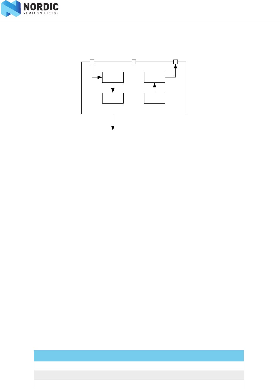
Page 137 of 195
nRF51 Series Reference Manual v2.0 - Serial Peripheral Interface (SPI) Master
25 Serial Peripheral Interface (SPI) Master
Figure 57 SPI master
Note: RXD-1 and TXD+1 illustrate the double buffered version of RXD and TXD respectively.
25.1 SPI master - functional description
The SPI master provides a simple CPU interface which includes a TXD register for sending data and an RXD
register for receiving data. These registers are double buffered to enable some degree of uninterrupted data
flow in and out of the SPI master. The SPI master does not implement support for chip select directly.
Therefore, the CPU must use available GPIOs to select the correct slave and control this independently of the
SPI master. The SPI master supports SPI modes 0 through 3.
25.1.1 SPI master mode pin configuration
The different signals SCK, MOSI, and MISO associated with the SPI master are mapped to physical pins
according to the configuration specified in the PSELSCK, PSELMOSI, and PSELMISO registers respectively. If a
value of 0xFFFFFFFF is specified in any of these registers, the associated SPI master signal is not connected
to any physical pin. The PSELSCK, PSELMOSI, and PSELMISO registers and their configurations are only used
as long as the SPI master is enabled, and retained only as long as the device is in ON mode.
To secure correct behavior in the SPI, the pins used by the SPI must be configured in the GPIO peripheral as
described in Table 34 prior to enabling the SPI. The SCK must always be connected to a pin, and that pin's
input buffer must always be connected for the SPI to work. This configuration must be retained in the GPIO
for the selected IOs as long as the SPI is enabled.
Only one peripheral can be assigned to drive a particular GPIO pin at a time, failing to do so may result in
unpredictable behavior.
Table 34 GPIO configuration
SPI master signal SPI master pin Direction Output value
SCK As specified in PSELSCK Output Same as CONFIG.CPOL
MOSI As specified in PSELMOSI Output 0
MISO As specified in PSELMISO Input Not applicable
RXD
READY
MISO MOSI
PSELMISO
RXD-1
TXD
TXD+1
PSELSCK PSELMOSI
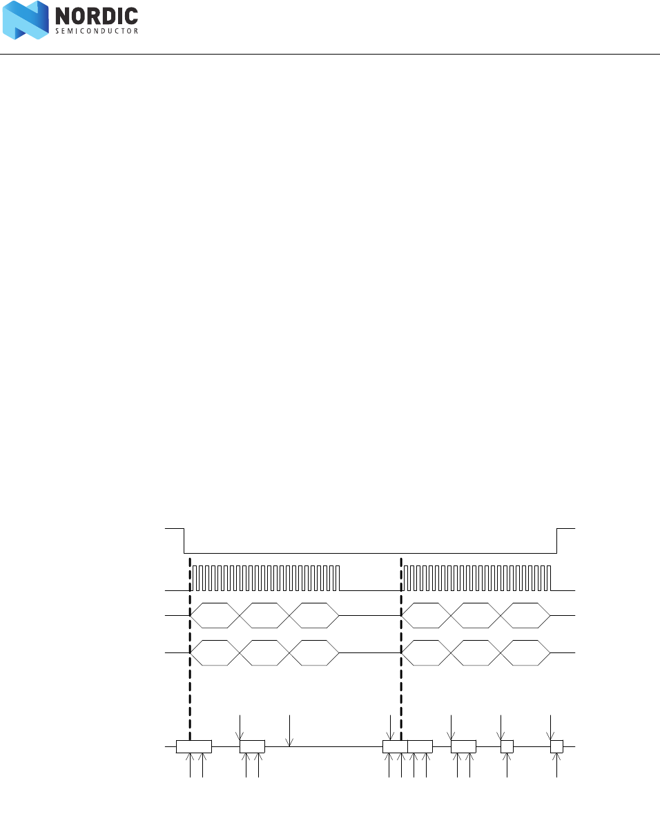
Page 138 of 195
nRF51 Series Reference Manual v2.0 - Serial Peripheral Interface (SPI) Master
25.1.2 Shared resources
The SPI shares registers and other resources with other peripherals that have the same ID as the SPI. The user
must therefore disable all peripherals that have the same ID as the SPI before the SPI can be configured and
used. Disabling a peripheral that have the same ID as the SPI will not reset any of the registers that are
shared with the SPI. It is therefore important to configure all relevant SPI registers explicitly to secure that it
operates correctly.
The Instantiation table in Section 4.2 “Instantiation” on page 13 shows which peripherals have the same ID
as the SPI.
25.1.3 SPI master transaction sequence
An SPI master transaction is started by writing the first byte, which is to be transmitted by the SPI master, to
the TXD register. Since the transmitter is double buffered, the second byte can be written to the TXD register
immediately after the first one. The SPI master will then send these bytes in the order they are written to the
TXD register.
The SPI master is a synchronous interface, and for every byte that is sent, a different byte will be received at
the same time; this is illustrated in Figure 58. Bytes that are received will be moved to the RXD register where
the CPU can extract them by reading the register. The RXD register is double buffered in the same way as the
TXD register, and a second byte can therefore be received at the same time as the first byte is being
extracted from RXD by the CPU. The SPI master will generate a READY event every time a new byte is moved
to the RXD register. The double buffered byte will be moved from RXD-1 to RXD as soon as the first byte is
extracted from RXD. The SPI master will stop when there are no more bytes to send in TXD and TXD+1.
Figure 58 SPI master transaction.
The READY event of the third byte transaction is delayed until B is extracted from RXD in occurrence number
3 on the horizontal lifeline. The reason for this is that the third event is generated first when C is moved from
RXD-1 to RXD after B is read.
012 n-2 n-1 n
ABC m-2 m-1 m
CS NMO SIMI SO
TX D = 0
TX D = 1
READY
Lifeline
A = RXD
TX D = 2
READY
B = RXD
TXD = n-2
C = RXD
TXD = n-1
READY
READY
READY
READY
m-2 = RXD
TX D = n
m-1 = RXD
m = RXD
SCK
1 3 4 5 6 72
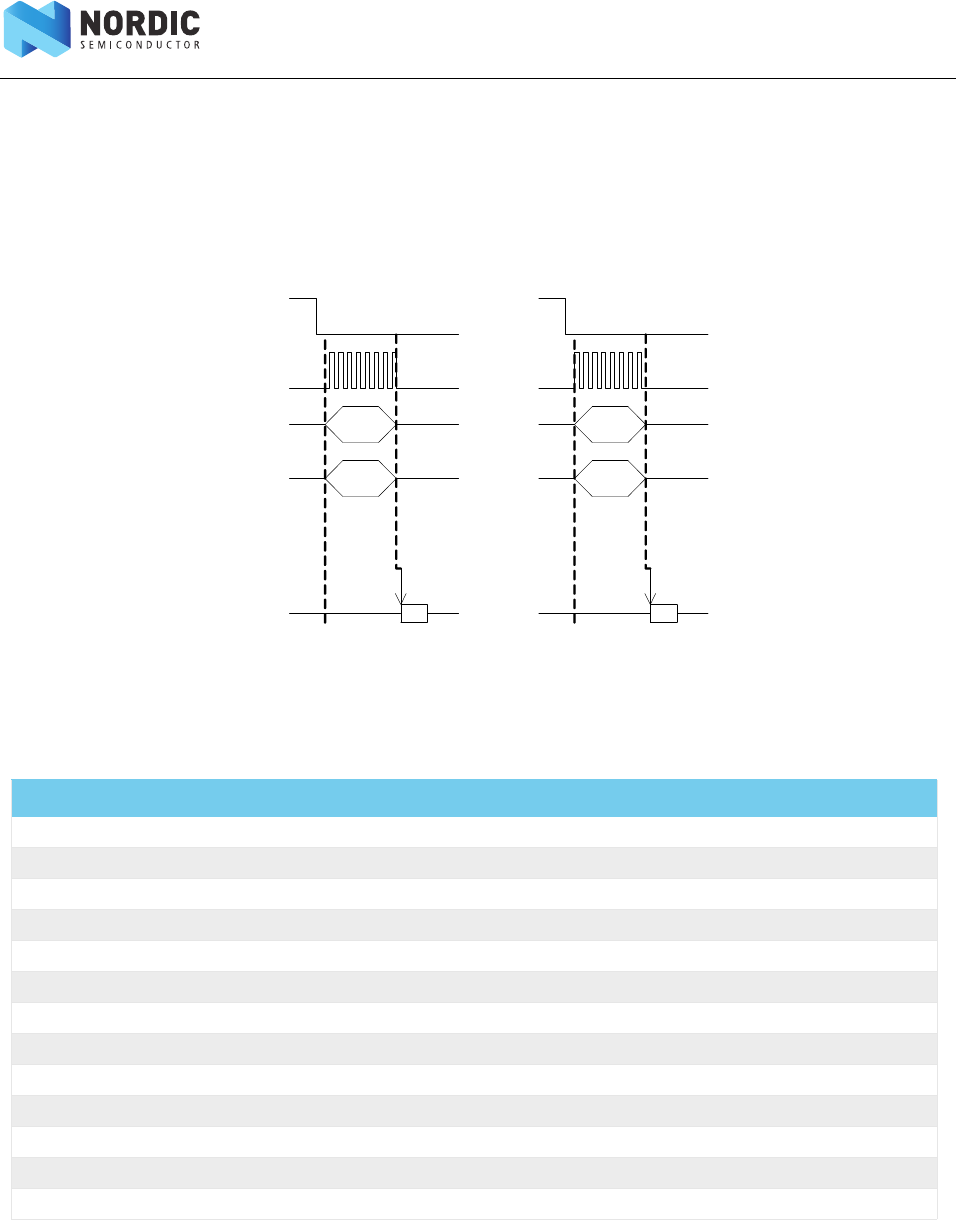
Page 139 of 195
nRF51 Series Reference Manual v2.0 - Serial Peripheral Interface (SPI) Master
The SPI master will move the incoming byte to the RXD register after a short delay following the SCK clock
period of the last bit in the byte. This also means that the READY event will be delayed accordingly, see
Figure 59. Therefore, it is important that you always clear the READY event, even if the RXD register and the
data that is being received is not used.
Figure 59 READY event timing details for SPI master mode for CPHA = 0 and CPHA = 1.
25.2 Registers
Table 35 Register overview
Register Offset Description
EVENTS
READY 0x108 TXD byte sent and RXD byte received
REGISTERS
INTENSET 0x304 Interrupt enable set register
INTENCLR 0x308 Interrupt enable clear register
ENABLE 0x500 Enable SPI
PSELSCK 0x508 Pin select for SCK
PSELMOSI 0x50C Pin select for MOSI
PSELMISO 0x510 Pin select for MISO
RXD 0x518 RXD register
TXD 0x51C TXD register
FREQUENCY 0x524 SPI frequency
CONFIG 0x554 Configuration register
MOSIMISO CSN
READY
Lifeline SCK
(CPHA=0)
1
MOSIMISO CSN
READY
Lifeline
SCK
(CPHA=1)
1

Page 140 of 195
nRF51 Series Reference Manual v2.0 - Serial Peripheral Interface (SPI) Master
25.2.1 RXD
25.2.2 TXD
25.2.3 ENABLE
25.2.4 PSELSCK
Bit number 31 30 29 28 27 26 25 24 23 22 21 20 19 18 17 16 15 14 13 12 11 10 9 8 7 6 5 4 3 2 1 0
ID (Field ID) ------------------------AAAAAAAA
Reset value 00000000000000000000000000000000
ID RW Field Value ID Value Description
A RW RX data received. Double buffered.
Bit number 31 30 29 28 27 26 25 24 23 22 21 20 19 18 17 16 15 14 13 12 11 10 9 8 7 6 5 4 3 2 1 0
ID (Field ID) - - - - - - - - - - - - - - - - - - - - - - - - A A A A A A A A
Reset value 0 0 0 0 0 0 0 0 0 0 0 0 0 0 0 0 0 0 0 0 0 0 0 0 0 0 0 0 0 0 0 0
ID RW Field Value ID Value Description
A RW TX data to send. Double buffered
Bit number 31 30 29 28 27 26 25 24 23 22 21 20 19 18 17 16 15 14 13 12 11 10 9 8 7 6 5 4 3 2 1 0
ID (Field ID) 00000000000000000000000000000AAA
Reset value 00000000000000000000000000000000
ID RW Field Value ID Value Description
A RW Enable or disable SPI
DISABLE 0Disable SPI
ENABLE 1 Enable SPI
Bit number 31 30 29 28 27 26 25 24 23 22 21 20 19 18 17 16 15 14 13 12 11 10 9 8 7 6 5 4 3 2 1 0
ID (Field ID) A A A A A A A A A A A A A A A A A A A A A A A A A A A A A A A A
Reset value 1 1 1 1 1 1 1 1 1 1 1 1 1 1 1 1 1 1 1 1 1 1 1 1 1 1 1 1 1 1 1 1
ID RW Field Value ID Value Description
A Pin number configuration for SPI SCK signal
RW [0..31] Pin number to route the SPI SCK signal to
W 0xFFFFFFFF Disconnect

Page 141 of 195
nRF51 Series Reference Manual v2.0 - Serial Peripheral Interface (SPI) Master
25.2.5 PSELMOSI
25.2.6 PSELMISO
25.2.7 CONFIG
Bit number 31 30 29 28 27 26 25 24 23 22 21 20 19 18 17 16 15 14 13 12 11 10 9 8 7 6 5 4 3 2 1 0
ID (Field ID) AAAAAAAAAAAAAAAAAAAAAAAAAAAAAAAA
Reset value 11111111111111111111111111111111
ID RW Field Value ID Value Description
A Pin number configuration for SPI MOSI signal
RW [0..31] Pin number to route the SPI MOSI signal to
W 0xFFFFFFFF Disconnect
Bit number 31 30 29 28 27 26 25 24 23 22 21 20 19 18 17 16 15 14 13 12 11 10 9 8 7 6 5 4 3 2 1 0
ID (Field ID) A A A A A A A A A A A A A A A A A A A A A A A A A A A A A A A A
Reset value 1 1 1 1 1 1 1 1 1 1 1 1 1 1 1 1 1 1 1 1 1 1 1 1 1 1 1 1 1 1 1 1
ID RW Field Value ID Value Description
A Pin number configuration for SPI master MISO signal
RW [0..31] Pin number to route the SPI master MISO signal to
W 0xFFFFFFFF Disconnect
Bit number 31 30 29 28 27 26 25 24 23 22 21 20 19 18 17 16 15 14 13 12 11 10 9 8 7 6 5 4 3 2 1 0
ID (Field ID) -----------------------------CBA
Reset value 00000000000000000000000000000000
ID RW Field Value ID Value Description
A RW ORDER Bit order
MSBFIRST 0Most significant bit shifted out first
LSBFIRST 1 Least significant bit shifted out first
BRW CPOL Serial clock (SCK) polarity
ACTIVEHIGH 0 Active high
ACTIVELOW 1Active low
C RW CPHA Serial clock (SCK) phase
LEADING 0Sample on leading edge of clock, shift serial data on trailing edge
TRAILING 1 Sample on trailing edge of clock, shift serial data on leading edge

Page 142 of 195
nRF51 Series Reference Manual v2.0 - Serial Peripheral Interface (SPI) Master
25.2.8 FREQUENCY
Bit number 31 30 29 28 27 26 25 24 23 22 21 20 19 18 17 16 15 14 13 12 11 10 9 8 7 6 5 4 3 2 1 0
ID (Field ID) A A A A A A A A A A A A A A A A A A A A A A A A A A A A A A A A
Reset value 0 0 0 0 0 0 0 0 0 0 0 0 0 0 0 0 0 0 0 0 0 0 0 0 0 0 0 0 0 0 0 0
ID RW Field Value ID Value Description
A RW SPI master data rate
K125 0x02000000 125 kbps
K250 0x04000000 250 kbps
K500 0x08000000 500 kbps
M1 0x10000000 1 Mbps
M2 0x20000000 2 Mbps
M4 0x40000000 4 Mbps
M8 0x80000000 8 Mbps
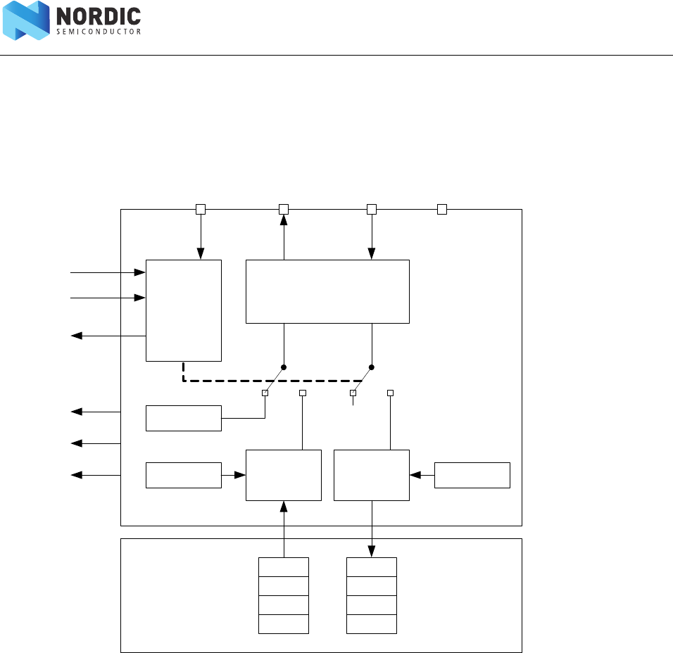
Page 143 of 195
nRF51 Series Reference Manual v2.0 - SPI Slave (SPIS)
26 SPI Slave (SPIS)
SPIS is a SPI slave with EasyDMA support for ultra low power serial communication from an external SPI
master. EasyDMA in conjunction with hardware based semaphore mechanisms removes all real-time
requirements associated with controlling the SPI slave from a low priority CPU execution context.
Figure 60 SPI slave
26.1 Pin configuration
The different signals CSN, SCK, MOSI, and MISO associated with the SPI slave are mapped to physical pins
according to the configuration specified in the PSELCSN, PSELSCK, PSELMOSI, and PSELMISO registers
respectively. If a value of 0xFFFFFFFF is specified in any of these registers, the associated SPI slave signal will
not be connected to any physical pins.
The PSELCSN, PSELSCK, PSELMOSI, and PSELMISO registers and their configurations are only used as long as
the SPI slave is enabled, and retained only as long as the device is in System ON mode, see Chapter 11
“Power management (POWER)” on page 40 for more information about power modes.
To secure correct behavior in the SPI slave, the pins used by the SPI slave must be configured in the GPIO
peripheral as described in Table 36 on page 144 prior to enabling the SPI slave. This is to secure that the pins
used by the SPI slave are driven correctly if the SPI slave itself is temporarily disabled or the device
temporarily enters System OFF. This configuration must be retained in the GPIO for the selected I/Os as long
as the SPI slave is to be recognized by an external SPI master.
The MISO line is set in high impedance as long as the SPI slave is not selected with CSN.
EasyDMA
RAM
SPIS
ACQUIRED
RXDPTRTXDPTR
TXD+1
TXD
TXD+n
TXD+2
RXD+1
RXD
RXD+n
RXD+2
EasyDMA
MISO MOSI
ACQUIRE
RELEASE
OVERFLOW
PSELMISO PSELMOSIPSELCSN PSELSCK
Semaphore
SPI slave tr anceiver
DEF
CSN
END
OVERREAD

Page 144 of 195
nRF51 Series Reference Manual v2.0 - SPI Slave (SPIS)
Only one peripheral can be assigned to drive a particular GPIO pin at a time, failing to do so may result in
unpredictable behavior.
Table 36 Pin configuration
26.2 Shared resources
The SPI slave shares registers and other resources with other peripherals that have the same ID as the SPI
slave. You must, therefore, disable all peripherals that have the same ID as the SPI slave before the SPI slave
can be configured and used. Disabling a peripheral that has the same ID as the SPI slave will not reset any of
the registers that are shared with the SPI slave. It is important to configure all relevant SPI slave registers
explicitly to secure that it operates correctly.
The Instantiation table in Section 4.2 “Instantiation” on page 13 shows which peripherals have the same ID
as the SPI slave.
26.3 EasyDMA
The SPI Slave implements EasyDMA for reading and writing to and from the RAM. The EasyDMA will have
finished accessing the RAM when the END event is generated.
26.4 SPI slave operation
SPI slave uses two memory pointers, RXDPTR and TXDPTR, that point to the RXD buffer (receive buffer) and
TXD buffer (transmit buffer) respectively, see Figure 60 on page 143. Since these buffers are located in RAM,
which can be accessed by both the SPI slave and the CPU, a hardware based semaphore mechanism is
implemented to enable safe sharing.
Before the CPU can safely update the RXDPTR and TXDPTR pointers it must first acquire the SPI semaphore.
The CPU can acquire the semaphore by triggering the ACQUIRE task and then receiving the ACQUIRED
event. When the CPU has updated the RXDPTR and TXDPTR pointers the CPU must release the semaphore
before the SPI slave will be able to acquire it. The CPU releases the semaphore by triggering the RELEASE
task. This is illustrated in Figure 61 on page 146. Triggering the RELEASE task when the semaphore is not
granted to the CPU will have no effect.
The semaphore mechanism does not, at any time, prevent the CPU from performing read or write access to
the RXDPTR register, the TXDPTR registers, or the RAM that these pointers are pointing to. The semaphore is
only telling when these can be updated by the CPU so that safe sharing is achieved.
The semaphore is by default assigned to the CPU after the SPI slave is enabled. No ACQUIRED event will be
generated for this initial semaphore handover. An ACQUIRED event will be generated immediately if the
ACQUIRE task is triggered while the semaphore is assigned to the CPU.
The SPI slave will try to acquire the semaphore when CSN goes low. If the SPI slave does not manage to
acquire the semaphore at this point, the transaction will be ignored. This means that all incoming data on
SPI signal SPI pin Direction Output value Comment
CSN As specified in PSELCSN Input Not applicable
SCK As specified in PSELSCK Input Not applicable
MOSI As specified in PSELMOSI Input Not applicable
MISO As specified in PSELMISO Input Not applicable Emulates that the SPI slave is not selected.

Page 145 of 195
nRF51 Series Reference Manual v2.0 - SPI Slave (SPIS)
MOSI will be discarded, and the DEF (default) character will be clocked out on the MISO line throughout the
whole transaction. This will also be the case even if the semaphore is released by the CPU during the
transaction. In case of a race condition where the CPU and the SPI slave try to acquire the semaphore at the
same time, as illustrated in lifeline item 2 in Figure 61 on page 146, the semaphore will be granted to the
CPU.
If the SPI slave acquires the semaphore, the transaction will be granted. The incoming data on MOSI will be
stored in the RXD buffer and the data in the TXD buffer will be clocked out on MISO.
When a granted transaction is completed and CSN goes high, the SPI slave will automatically release the
semaphore and generate the END event.
As long as the semaphore is available the SPI slave can be granted multiple transactions one after the other.
If the CPU is not able to reconfigure the TXDPTR and RXDPTR between granted transactions, the same TX
data will be clocked out and the RX buffers will be overwritten. To prevent this from happening, the
END_ACQUIRE shortcut can be used. With this shortcut enabled the semaphore will be handed over to the
CPU automatically after the granted transaction has completed, giving the CPU the ability to update the
TXDPTR and RXDPTR between every granted transaction.
If the CPU tries to acquire the semaphore while it is assigned to the SPI slave, an immediate handover will
not be granted. However, the semaphore will be handed over to the CPU as soon as the SPI slave has
released the semaphore after the granted transaction is completed. If the END_ACQUIRE shortcut is enabled
and the CPU has triggered the ACQUIRE task during a granted transaction, only one ACQUIRE request will be
served following the END event.
The MAXRX register specifies the maximum number of bytes the SPI slave can receive in one granted
transaction. If the SPI slave receives more than MAXRX number of bytes, an OVERFLOW will be indicated in
the STATUS register and the incoming bytes will be discarded.
The MAXTX parameter specifies the maximum number of bytes the SPI slave can transmit in one granted
transaction. If the SPI slave is forced to transmit more than MAXTX number of bytes, an OVERREAD will be
indicated in the STATUS register and the ORC character will be clocked out.
The AMOUNTRX and AMOUNTTX registers are updated when a granted transaction is completed. The
AMOUNTTX register indicates how many bytes were read from the TX buffer in the last transaction, that is,
ORC (over-read) characters are not included in this number. Similarly, the AMOUNTRX register indicates how
many bytes were written into the RX buffer in the last transaction.
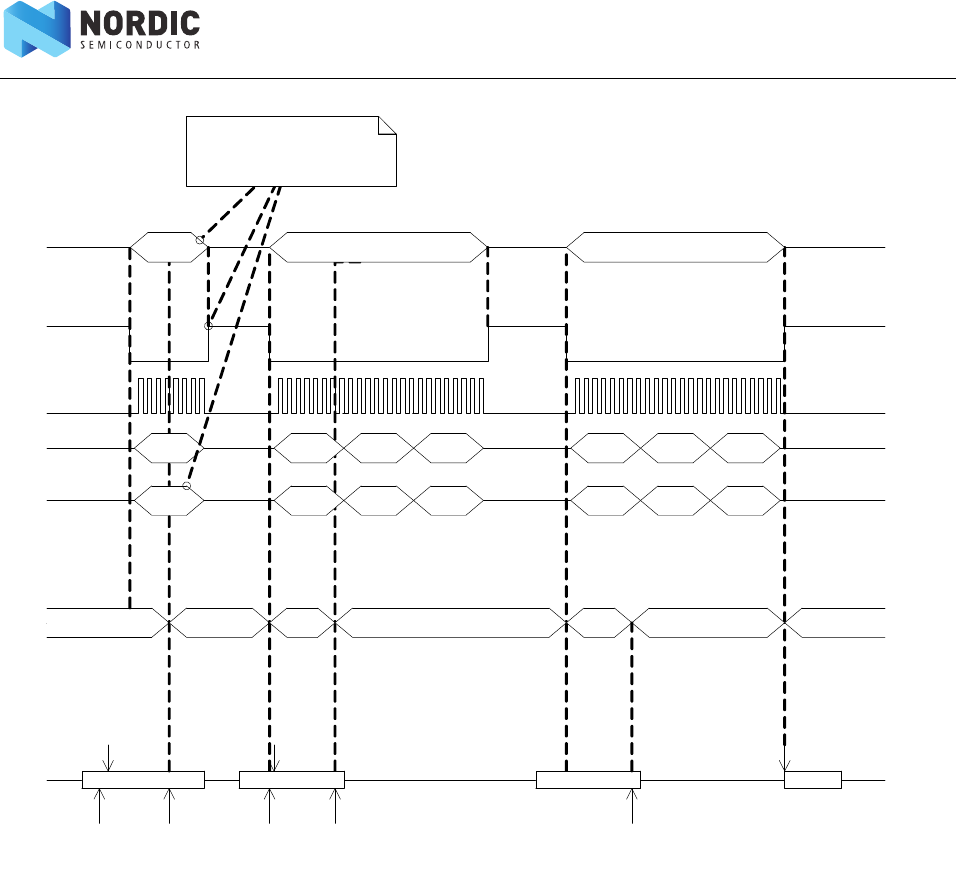
Page 146 of 195
nRF51 Series Reference Manual v2.0 - SPI Slave (SPIS)
Figure 61 SPI transaction when shortcut between END and ACQUIRE is enabled.
0 0 1 2
DEF ABC
CSNMOSIMISO
ACQUIRE
Lifeline
ACQUIRED
SCK
41
RELEASE
END
&
ACQUIRED
Se ma ph or e assi gn me nt
CPU Free CPUPENDING CPU
Transaction status
Ignored Granted
3
ACQUIRE
Ignored
0
DEF
CPU
2
ACQUIRE
RELEASE
Free
ACQUIRED
1
DEF
SPI master can use the DEF
character to stop the transaction as
soon as possible if the transaction is
not gr anted .
2
DEF
SPIS

Page 147 of 195
nRF51 Series Reference Manual v2.0 - SPI Slave (SPIS)
26.5 Registers
Table 37 Register overview
26.5.1 SHORTS
Register Offset Description Support
TASKS
ACQUIRE 0x024 Acquire SPI semaphore. S
RELEASE 0x028 Release SPI semaphore, enabling the SPI slave to acquire it. S
EVENTS
END 0x104 Granted transaction completed. S
ACQUIRED 0x128 Semaphore acquired. S
REGISTERS
SHORTS 0x200 Shortcut for the SPI slave. S
INTENSET 0x304 Interrupt enable set register. S
INTENCLR 0x308 Interrupt enable clear register. S
SEMSTAT 0x400 Semaphore status register. S
STATUS 0x440 Status from last transaction. S
ENABLE 0x500 Enable SPI slave. S
PSELSCK 0x508 Pin select for SCK. S
PSELMISO 0x50C Pin select for MISO. S
PSELMOSI 0x510 Pin select for MOSI. S
PSELCSN 0x514 Pin select for CSN. S
RXDPTR 0x534 RXD data pointer. S
MAXRX 0x538 Maximum number of bytes in receive buffer. S
AMOUNTRX 0x53C Number of bytes received in last granted transaction. S
TXDPTR 0x544 TXD data pointer. S
MAXTX 0x548 Maximum number of bytes in transmit buffer. S
AMOUNTTX 0x54C Number of bytes transmitted in last granted transaction. S
CONFIG 0x554 Configuration register. S
DEF 0x55C Default character. Character clocked out in case of an ignored transaction. S
ORC 0x5C0 Over-read character. Character clocked out after an over-read of the transmit
buffer.
S
Bit number 31 30 29 28 27 26 25 24 23 22 21 20 19 18 17 16 15 14 13 12 11 10 9 8 7 6 5 4 3 2 1 0
ID (Field ID) - - - - - - - - - - - - - - - - - - - - - - - - - - - - - A - -
Reset value 0 0 0 0 0 0 0 0 0 0 0 0 0 0 0 0 0 0 0 0 0 0 0 0 0 0 0 0 0 0 0 0
ID RW Field Value ID Value Description
A RW END_ACQUIRE Enable or disable shortcut between END event and ACQUIRE task.

Page 148 of 195
nRF51 Series Reference Manual v2.0 - SPI Slave (SPIS)
26.5.2 ENABLE
26.5.3 SEMSTAT
26.5.4 STATUS
Individual status bits are cleared by writing a '1' to the bits that shall be cleared.
26.5.5 RXDPTR
Bit number 31 30 29 28 27 26 25 24 23 22 21 20 19 18 17 16 15 14 13 12 11 10 9 8 7 6 5 4 3 2 1 0
ID (Field ID) 0 0 0 0 0 0 0 0 0 0 0 0 0 0 0 0 0 0 0 0 0 0 0 0 0 0 0 0 0 A A A
Reset value 0 0 0 0 0 0 0 0 0 0 0 0 0 0 0 0 0 0 0 0 0 0 0 0 0 0 0 0 0 0 0 0
ID RW Field Value ID Value Description
ARW
DISABLE
ENABLE
0
2
Enable or disable SPI slave
Disable SPI slave
Enable SPI slave
Bit number 31 30 29 28 27 26 25 24 23 22 21 20 19 18 17 16 15 14 13 12 11 10 9 8 7 6 5 4 3 2 1 0
ID (Field ID) - - - - - - - - - - - - - - - - - - - - - - - - - - - - - - A A
Reset value 0 0 0 0 0 0 0 0 0 0 0 0 0 0 0 0 0 0 0 0 0 0 0 0 0 0 0 0 0 0 0 1
ID RW Field Value ID Value Description
AR
Free
CPU
SPIS
CPUENDING
0
1
2
3
Semaphore status.
Semaphore is free.
Semaphore is assigned to CPU.
Semaphore is assigned to SPI slave.
Semaphore is assigned to SPI but a handover to the CPU is pending.
Bit number 31 30 29 28 27 26 25 24 23 22 21 20 19 18 17 16 15 14 13 12 11 10 9 8 7 6 5 4 3 2 1 0
ID (Field ID) - - - - - - - - - - - - - - - - - - - - - - - - - - - - - - B A
Reset value 0 0 0 0 0 0 0 0 0 0 0 0 0 0 0 0 0 0 0 0 0 0 0 0 0 0 0 0 0 0 0 0
ID RW Field Value ID Value Description
A
B
RW
RW
OVERREAD
OVERFLOW
TX buffer over-read detected and prevented.
RX buffer overflow detected and prevented.
Bit number 31 30 29 28 27 26 25 24 23 22 21 20 19 18 17 16 15 14 13 12 11 10 9 8 7 6 5 4 3 2 1 0
ID (Field ID) A A A A A A A A A A A A A A A A A A A A A A A A A A A A A A A A
Reset value 0 0 0 0 0 0 0 0 0 0 0 0 0 0 0 0 0 0 0 0 0 0 0 0 0 0 0 0 0 0 0 0
ID RW Field Value ID Value Description
ARW RXD data pointer

Page 149 of 195
nRF51 Series Reference Manual v2.0 - SPI Slave (SPIS)
26.5.6 TXDPTR
26.5.7 PSELCSN
26.5.8 PSELSCK
26.5.9 PSELMOSI
Bit number 31 30 29 28 27 26 25 24 23 22 21 20 19 18 17 16 15 14 13 12 11 10 9 8 7 6 5 4 3 2 1 0
ID (Field ID) A A A A A A A A A A A A A A A A A A A A A A A A A A A A A A A A
Reset value 0 0 0 0 0 0 0 0 0 0 0 0 0 0 0 0 0 0 0 0 0 0 0 0 0 0 0 0 0 0 0 0
ID RW Field Value ID Value Description
A RW TXD data pointer
Bit number 31 30 29 28 27 26 25 24 23 22 21 20 19 18 17 16 15 14 13 12 11 10 9 8 7 6 5 4 3 2 1 0
ID (Field ID) A A A A A A A A A A A A A A A A A A A A A A A A A A A A A A A A
Reset value 1 1 1 1 1 1 1 1 1 1 1 1 1 1 1 1 1 1 1 1 1 1 1 1 1 1 1 1 1 1 1 1
ID RW Field Value ID Value Description
A
RW
W
[0..31]
0xFFFFFFFF
Pin number configuration for SPI CSN signal.
Pin number to route the SPI CSN signal to.
Disconnect.
Bit number 31 30 29 28 27 26 25 24 23 22 21 20 19 18 17 16 15 14 13 12 11 10 9 8 7 6 5 4 3 2 1 0
ID (Field ID) A A A A A A A A A A A A A A A A A A A A A A A A A A A A A A A A
Reset value 1 1 1 1 1 1 1 1 1 1 1 1 1 1 1 1 1 1 1 1 1 1 1 1 1 1 1 1 1 1 1 1
ID RW Field Value ID Value Description
A
RW
W
[0..31]
0xFFFFFFFF
Pin number configuration for SPI SCK signal.
Pin number to route the SPI SCK signal to.
Disconnect.
Bit number 31 30 29 28 27 26 25 24 23 22 21 20 19 18 17 16 15 14 13 12 11 10 9 8 7 6 5 4 3 2 1 0
ID (Field ID) A A A A A A A A A A A A A A A A A A A A A A A A A A A A A A A A
Reset value 1 1 1 1 1 1 1 1 1 1 1 1 1 1 1 1 1 1 1 1 1 1 1 1 1 1 1 1 1 1 1 1
ID RW Field Value ID Value Description
A
RW
W
[0..31]
0xFFFFFFFF
Pin number configuration for SPI MOSI signal.
Pin number to route the SPI MOSI signal to.
Disconnect.

Page 150 of 195
nRF51 Series Reference Manual v2.0 - SPI Slave (SPIS)
26.5.10 PSELMISO
26.5.11 CONFIG
26.5.12 DEF
26.5.13 ORC
Bit number 31 30 29 28 27 26 25 24 23 22 21 20 19 18 17 16 15 14 13 12 11 10 9 8 7 6 5 4 3 2 1 0
ID (Field ID) A A A A A A A A A A A A A A A A A A A A A A A A A A A A A A A A
Reset value 1 1 1 1 1 1 1 1 1 1 1 1 1 1 1 1 1 1 1 1 1 1 1 1 1 1 1 1 1 1 1 1
ID RW Field Value ID Value Description
A
RW
W
[0..31]
0xFFFFFFFF
Pin number configuration for SPI MISO signal.
Pin number to route the SPI MISO signal to.
Disconnect.
Bit number 31 30 29 28 27 26 25 24 23 22 21 20 19 18 17 16 15 14 13 12 11 10 9 8 7 6 5 4 3 2 1 0
ID (Field ID) - - - - - - - - - - - - - - - - - - - - - - - - - - - - - C B A
Reset value 0 0 0 0 0 0 0 0 0 0 0 0 0 0 0 0 0 0 0 0 0 0 0 0 0 0 0 0 0 0 0 0
ID RW Field Value ID Value Description
A
B
C
RW
RW
RW
ORDER
CPHA
CPOL
MSBFIRST
LSBFIRST
LEADING
TRAILING
ACTIVEHIGH
ACTIVELOW
0
1
0
1
0
1
Bit order.
Most significant bit shifted out first.
Least significant bit shifted out first.
Serial clock (SCK) phase.
Sample on leading edge of clock, shift serial data on trailing edge.
Sample on trailing edge of clock, shift serial data on leading edge.
Serial clock (SCK) polarity.
Active high.
Active low.
Bit number 31 30 29 28 27 26 25 24 23 22 21 20 19 18 17 16 15 14 13 12 11 10 9 8 7 6 5 4 3 2 1 0
ID (Field ID) - - - - - - - - - - - - - - - - - - - - - - - - A A A A A A A A
Reset value 0 0 0 0 0 0 0 0 0 0 0 0 0 0 0 0 0 0 0 0 0 0 0 0 0 0 0 0 0 0 0 0
ID RW Field Value ID Value Description
A RW Default character. Clocked out on MISO during an ignored transaction.
Bit number 31 30 29 28 27 26 25 24 23 22 21 20 19 18 17 16 15 14 13 12 11 10 9 8 7 6 5 4 3 2 1 0
ID (Field ID) - - - - - - - - - - - - - - - - - - - - - - - - A A A A A A A A
Reset value 0 0 0 0 0 0 0 0 0 0 0 0 0 0 0 0 0 0 0 0 0 0 0 0 0 0 0 0 0 0 0 0
ID RW Field Value ID Value Description
A RW Over-read character. Character clocked out after an over-read of the transmit
buffer.

Page 151 of 195
nRF51 Series Reference Manual v2.0 - SPI Slave (SPIS)
26.5.14 MAXRX
26.5.15 MAXTX
26.5.16 AMOUNTRX
26.5.17 AMOUNTTX
Bit number 31 30 29 28 27 26 25 24 23 22 21 20 19 18 17 16 15 14 13 12 11 10 9 8 7 6 5 4 3 2 1 0
ID (Field ID) - - - - - - - - - - - - - - - - - - - - - - - - A A A A A A A A
Reset value 0 0 0 0 0 0 0 0 0 0 0 0 0 0 0 0 0 0 0 0 0 0 0 0 0 0 0 0 0 0 0 0
ID RW Field Value ID Value Description
A RW Maximum number of bytes in receive buffer.
Bit number 31 30 29 28 27 26 25 24 23 22 21 20 19 18 17 16 15 14 13 12 11 10 9 8 7 6 5 4 3 2 1 0
ID (Field ID) - - - - - - - - - - - - - - - - - - - - - - - - A A A A A A A A
Reset value 0 0 0 0 0 0 0 0 0 0 0 0 0 0 0 0 0 0 0 0 0 0 0 0 0 0 0 0 0 0 0 0
ID RW Field Value ID Value Description
A RW Maximum number of bytes in transmit buffer.
Bit number 31 30 29 28 27 26 25 24 23 22 21 20 19 18 17 16 15 14 13 12 11 10 9 8 7 6 5 4 3 2 1 0
ID (Field ID) - - - - - - - - - - - - - - - - - - - - - - - - A A A A A A A A
Reset value 0 0 0 0 0 0 0 0 0 0 0 0 0 0 0 0 0 0 0 0 0 0 0 0 0 0 0 0 0 0 0 0
ID RW Field Value ID Value Description
A RW Number of bytes received in the last granted transaction.
Bit number 31 30 29 28 27 26 25 24 23 22 21 20 19 18 17 16 15 14 13 12 11 10 9 8 7 6 5 4 3 2 1 0
ID (Field ID) - - - - - - - - - - - - - - - - - - - - - - - - A A A A A A A A
Reset value 0 0 0 0 0 0 0 0 0 0 0 0 0 0 0 0 0 0 0 0 0 0 0 0 0 0 0 0 0 0 0 0
ID RW Field Value ID Value Description
A RW Number of bytes transmitted in the last granted transaction.
Page 152 of 195
nRF51 Series Reference Manual v2.0 - I2C compatible Two Wire Interface (TWI)
27 I2C compatible Two Wire Interface (TWI)
Figure 62 TWI master’s main features
27.1 Functional description
The TWI master is compatible with I2C operating at 100 kHz and 400 kHz. This TWI master is not compatible
with CBUS. As illustrated in Figure 62, the TWI transmitter and receiver are single buffered.
A TWI setup comprising one master and three slaves is illustrated in Figure 63. This TWI master is only able to
operate as the only master on the TWI bus.
Figure 63 A typical TWI setup comprising one master and three slaves
This TWI master supports clock stretching performed by the slaves. The TWI master is started by triggering
the STARTTX or STARTRX tasks, and stopped by triggering the STOP task.
If a NACK is clocked in from the slave, the TWI master will generate an ERROR event.
27.2 Master mode pin configuration
The different signals SCL and SDA associated with the TWI master are mapped to physical pins according to
the configuration specified in the PSELSCL and PSELSDA registers respectively. If a value of 0xFFFFFFFF is
specified in any of these registers, the associated TWI master signal is not connected to any physical pin. The
PSELSCL and PSELSDA registers and their configurations are only used as long as the TWI master is enabled,
and retained only as long as the device is in ON mode. To secure correct signal levels on the pins used by the
TWI master when the system is in OFF mode, and when the TWI master is disabled, these pins must be
configured in the GPIO peripheral as described in Table 38 on page 153.
TXD
(signal)
RXD TXD
PSELSDAPSELSCKPSELSDA
RXD
(signal) ERROR
STOP
STARTTX
STARTRX
STOPPED
RXDRDY
TXDSENT
BBSUSPEND
RESUME
TWI master
TWI slave
(Sensor)
Address = b1011000
TWI slave
Address = b1011011
SCL SDA
TWI slave
(EEPROM)
Address = b1011001
SDA
R
VDD
R
VDD
SDA SCL SCL SDA SCL

Page 153 of 195
nRF51 Series Reference Manual v2.0 - I2C compatible Two Wire Interface (TWI)
Only one peripheral can be assigned to drive a particular GPIO pin at a time, failing to do so may result in
unpredictable behavior.
Table 38 GPIO configuration
27.3 Shared resources
The TWI shares registers and other resources with other peripherals that have the same ID as the TWI.
Therefore, you must disable all peripherals that have the same ID as the TWI before the TWI can be
configured and used. Disabling a peripheral that has the same ID as the TWI will not reset any of the
registers that are shared with the TWI. It is therefore important to configure all relevant TWI registers
explicitly to secure that it operates correctly.
The Instantiation table in Section 4.2 “Instantiation” on page 13 shows which peripherals have the same ID
as the TWI.
27.4 Master write sequence
A TWI master write sequence is started by triggering the STARTTX task. After the STARTTX task has been
triggered, the TWI master will generate a start condition on the TWI bus, followed by clocking out the
address and the READ/WRITE bit set to 0 (WRITE=0, READ=1). The address must match the address of the
slave device that the master wants to write to. The READ/WRITE bit is followed by an ACK/NACK bit (ACK=0
or NACK=1) generated by the slave.
After receiving the ACK/NACK bit, the TWI master will clock out the data bytes that are written to the TXD
register. Each byte clocked out from the master will be followed by an ACK/NACK bit clocked in from the
slave. A TXDSENT event will be generated each time the TWI master has clocked out a TXD byte, and the
associated ACK/NACK bit has been clocked in from the slave.
The TWI master transmitter is single buffered, and a second byte can only be written to the TXD register
after the previous byte has been clocked out and the ACK/NACK bit clocked in, that is, after the TXDSENT
event has been generated.
If the CPU is prevented from writing to TXD when the TWI master is ready to clock out a byte, the TWI master
will stretch the clock until the CPU has written a byte to the TXD register.
A typical TWI master write sequence is illustrated in Figure 64 on page 154. Occurrence 3 in Figure 64 on
page 154 illustrates delayed processing of the TXDSENT event associated with TXD byte 1. In this scenario
the TWI master will stretch the clock to prevent writing erroneous data to the slave.
TWI master signal TWI master pin Direction Drive strength Output value
SCL As specified in PSELSCL Input S0D1 Not applicable
SDA As specified in PSELSDA Input S0D1 Not applicable
Page 154 of 195
nRF51 Series Reference Manual v2.0 - I2C compatible Two Wire Interface (TWI)
Figure 64 The TWI master writing data to a slave.
The TWI master write sequence is stopped when the STOP task is triggered. When the STOP task is triggered,
the TWI master will generate a stop condition on the TWI bus.
27.5 Master read sequence
A TWI master read sequence is started by triggering the STARTRX task. After the STARTRX task has been
triggered the TWI master will generate a start condition on the TWI bus, followed by clocking out the
address and the READ/WRITE bit set to 1 (WRITE = 0, READ = 1). The address must match the address of the
slave device that the master wants to read from. The READ/WRITE bit is followed by an ACK/NACK bit (ACK=0
or NACK = 1) generated by the slave.
After having sent the ACK/NACK bit the TWI slave will send data to the master using the clock generated by
the master.
The TWI master will generate a RXDRDY event every time a new byte is received in the RXD register.
After receiving a byte, the TWI master will delay sending the ACK/NACK bit by stretching the clock until the
CPU has extracted the received byte, that is, by reading the RXD register.
The TWI master read sequence is stopped by triggering the STOP task. This task must be triggered before
the last byte is extracted from RXD to ensure that the TWI master sends a NACK back to the slave before
generating the stop condition.
A typical TWI master read sequence is illustrated in Figure 65 on page 155. Occurrence 3 in Figure 65 on
page 155 illustrates delayed processing of the RXDRDY event associated with RXD byte B. In this scenario
the TWI master will stretch the clock to prevent the slave from overwriting the contents of the RXD register.
67$577;
7;'6(17
&38/LIHOLQH
7;'
7;'
7;'6(17
7;'6(17
67$57
$''5
$&.
$&.
$&.
1
$&.
1
$&.
6723
7:,
6723
$&.
7;'
7;'6(17
7;' 1
:5,7(
67233('
Page 155 of 195
nRF51 Series Reference Manual v2.0 - I2C compatible Two Wire Interface (TWI)
Figure 65 The TWI master reading data from a slave.
67$575;
&38/LIHOLQH
$ 5;'
5;'5'<
5;'5'<
67$57
$''5
$&.
$
$&.
0
$&.
0
1$&.
6723
7:,
%
$&.
5;'5'<
0 5;'
5($'
67233('
5(680(
%%
6863(1'
6+257
%%
6863(1'
6+257
7:,/LIHOLQH
%%
6863(1'
6+257
%%
6723
6+257
5(680(
0 5;'
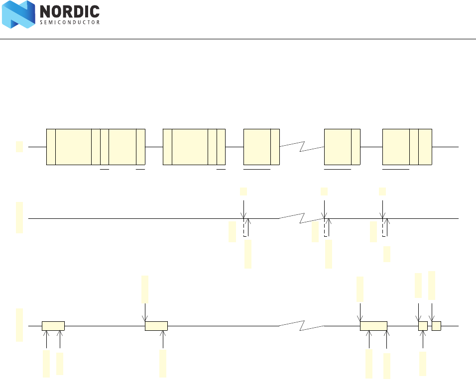
Page 156 of 195
nRF51 Series Reference Manual v2.0 - I2C compatible Two Wire Interface (TWI)
27.6 Master repeated start sequence
Figure 66 illustrates a typical repeated start sequence where the TWI master writes one byte to the slave
followed by reading M bytes from the slave. Any combination and number of transmit and receive
sequences can be combined in this fashion. Only one shortcut to STOP can be enabled at any given time.
Figure 66 A repeated start sequence, where the TWI master writes one byte, followed by reading M bytes from
the slave without performing a stop in-between
To generate a repeated start after a read sequence, a second start task must be triggered instead of the STOP
task, that is, STARTRX or STARTTX. This start task must be triggered before the last byte is extracted from
RXD to ensure that the TWI master sends a NACK back to the slave before generating the repeated start
condition.
67$577;
7;'6(17
&38/LIHOLQH
67$575;
5;'5'<
67$57
$''5
$&.
$&.
$
$&.
0
$&.
0
1$&.
6723
7:,
7;'
5;'5'<
0 5;'
:5,7(
67233('
%%
6863(1'
6+257
7:,/LIHOLQH
%%
6863(1'
6+257
%%
6723
6+257
5(680(
0 5;'
67$57
$''5
$&.
5($'

Page 157 of 195
nRF51 Series Reference Manual v2.0 - I2C compatible Two Wire Interface (TWI)
27.7 Registers
Table 39 Register overview
27.7.1 SHORTS
Register Offset Description
TASKS
STARTRX 0x000 Start TWI receive sequence
STARTTX 0x008 Start TWI transmit sequence
STOP 0x014 Stop TWI transaction
SUSPEND 0x01C Suspend TWI transaction
RESUME 0x020 Resume TWI transaction
EVENTS
STOPPED 0x104 TWI stopped
RXDRDY 0x108 TWI RXD byte received
TXDSENT 0x11C TWI TXD byte sent
ERROR 0x124 TWI error
BB 0x138 TWI byte boundary, generated before each byte that is sent or received
REGISTERS
SHORTS 0x200 Shortcut register
INTENSET 0x304 Interrupt enable set register
INTENCLR 0x308 Interrupt enable clear register
ERRORSRC 0x4C4 TWI error source
ENABLE 0x500 Enable TWI master
PSELSCL 0x508 Pin select for SCL
PSELSDA 0x50C Pin select for SDA
RXD 0x518 RXD register
TXD 0x51C TXD register
FREQUENCY 0x524 TWI frequency
ADDRESS 0x588 Address used in the TWI transfer
Bit number 31 30 29 28 27 26 25 24 23 22 21 20 19 18 17 16 15 14 13 12 11 10 9 8 7 6 5 4 3 2 1 0
ID (Field ID) ------------------------------BA
Reset value 00000000000000000000000000000000
ID RW Field Value
ID Value Description
A RW BB_SUSPEND
0
1
Short-cut between BB event and SUSPEND task
Disable
Enable
BRW BB_STOP
0
1
Short-cut between BB event and STOP task
Disable
Enable

Page 158 of 195
nRF51 Series Reference Manual v2.0 - I2C compatible Two Wire Interface (TWI)
27.7.2 ERRORSRC
27.7.3 ENABLE
27.7.4 PSELSCL
27.7.5 PSELSDA
Bit number 31 30 29 28 27 26 25 24 23 22 21 20 19 18 17 16 15 14 13 12 11 10 9 8 7 6 5 4 3 2 1 0
ID (Field ID) - - - - - - - - - - - - - - - - - - - - - - - - - - - - - C B -
Reset value 0 0 0 0 0 0 0 0 0 0 0 0 0 0 0 0 0 0 0 0 0 0 0 0 0 0 0 0 0 0 0 0
ID RW Field Value ID Value Description
B RW ANACK 1 NACK received after sending the address (write ‘1’ to clear)
CRW DNACK 1NACK received after sending a data byte (write ‘1’ to clear)
Bit number 31 30 29 28 27 26 25 24 23 22 21 20 19 18 17 16 15 14 13 12 11 10 9 8 7 6 5 4 3 2 1 0
ID (Field ID) 00000000000000000000000000000AAA
Reset value 00000000000000000000000000000000
ID RW Field Value ID Value Description
A RW ENABLE Enable or disable TWI
DISABLE 0Disable TWI
ENABLE 5 Enable TWI
Bit number 31 30 29 28 27 26 25 24 23 22 21 20 19 18 17 16 15 14 13 12 11 10 9 8 7 6 5 4 3 2 1 0
ID (Field ID) A A A A AAAAAAAAAAAAAAAAAAAAAAAAAAAA
Reset value 1 1 1 1 1111111111111111111111111111
ID RW Field Value ID Value Description
A Pin number configuration for TWI SCL signal
RW [0..31] Pin number to route the TWI SCL signal to
W 0xFFFFFFFF Disconnect
Bit number 31 30 29 28 27 26 25 24 23 22 21 20 19 18 17 16 15 14 13 12 11 10 9 8 7 6 5 4 3 2 1 0
ID (Field ID) A A A A A A A A A A A A A A A A A A A A A A A A A A A A A A A A
Reset value 1 1 1 1 1 1 1 1 1 1 1 1 1 1 1 1 1 1 1 1 1 1 1 1 1 1 1 1 1 1 1 1
ID RW Field Value ID Value Description
A Pin number configuration for TWI SDA signal
RW [0..31] Pin number to route the TWI SDA signal to
W 0xFFFFFFFF Disconnect

Page 159 of 195
nRF51 Series Reference Manual v2.0 - I2C compatible Two Wire Interface (TWI)
27.7.6 RXD
27.7.7 TXD
27.7.8 FREQUENCY
27.7.9 ADDRESS
Bit number 31 30 29 28 27 26 25 24 23 22 21 20 19 18 17 16 15 14 13 12 11 10 9 8 7 6 5 4 3 2 1 0
ID (Field ID) ------------------------AAAAAAAA
Reset value 00000000000000000000000000000000
ID RW Field Value ID Value Description
A RW RX data from last transfer
Bit number 31 30 29 28 27 26 25 24 23 22 21 20 19 18 17 16 15 14 13 12 11 10 9 8 7 6 5 4 3 2 1 0
ID (Field ID) - - - - - - - - - - - - - - - - - - - - - - - - A A A A A A A A
Reset value 0 0 0 0 0 0 0 0 0 0 0 0 0 0 0 0 0 0 0 0 0 0 0 0 0 0 0 0 0 0 0 0
ID RW Field Value ID Value Description
A RW TX data for next transfer
Bit number 31 30 29 28 27 26 25 24 23 22 21 20 19 18 17 16 15 14 13 12 11 10 9 8 7 6 5 4 3 2 1 0
ID (Field ID) A A A A AAAAAAAAAAAAAAAAAAAAAAAAAAAA
Reset value 0 0 0 0 0100000000000000000000000000
ID RW Field Value ID Value Description
A RW TWI master clock frequency
K100 0x01980000 100 kbps
K250 0x4000000 250 kbps
K400 0x06680000 400 kbps
Bit number 31 30 29 28 27 26 25 24 23 22 21 20 19 18 17 16 15 14 13 12 11 10 9 8 7 6 5 4 3 2 1 0
ID (Field ID) -------------------------AAAAAAA
Reset value 00000000000000000000000000000000
ID RW Field Value ID Value Description
A RW TWI address
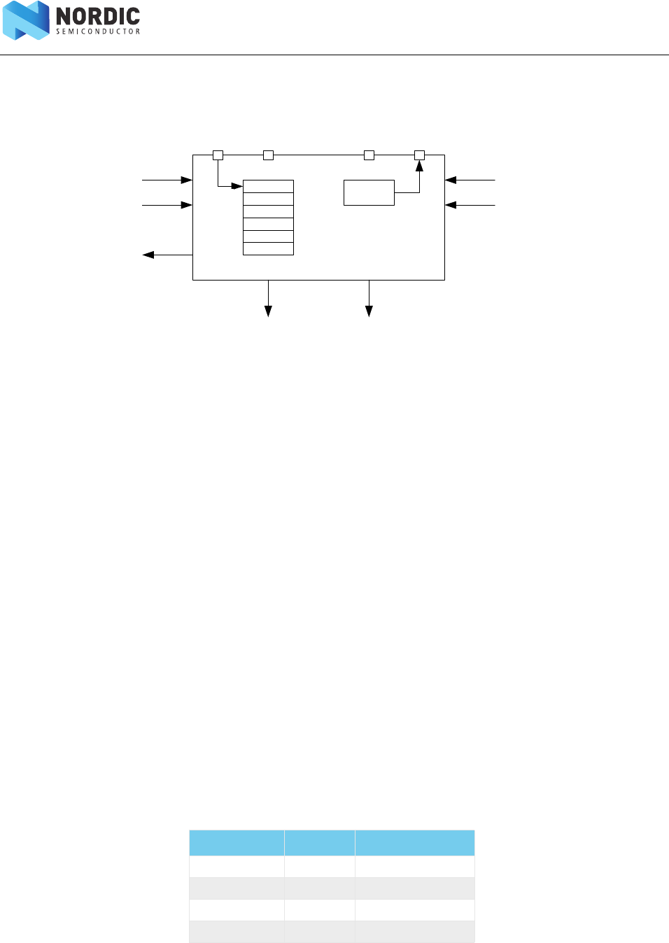
Page 160 of 195
nRF51 Series Reference Manual v2.0 - Universal Asynchronous Receiver/Transmitter (UART)
28 Universal Asynchronous Receiver/Transmitter (UART)
Figure 67 UART configuration
28.1 Functional description
The UART implements support for the following features:
•Full-duplex operation
• Automatic flow control
• Parity checking and generation for the 9th data bit
As illustrated in Figure 67, the UART uses the TXD and RXD registers directly to transmit and receive data.
The UART uses one stop bit.
28.2 Pin configuration
The different signals RXD, CTS (Clear To Send, active low), RTS (Request To Send, active low), and TXD
associated with the UART are mapped to physical pins according to the configuration specified in the
PSELRXD, PSELCTS, PSELRTS, and PSELTXD registers respectively. If a value of 0xFFFFFFFF is specified in any
of these registers, the associated UART signal will not be connected to any physical pin. The PSELRXD,
PSELCTS, PSELRTS, and PSELTXD registers and their configurations are only used as long as the UART is
enabled, and retained only for the duration the device is in ON mode. To secure correct signal levels on the
pins by the UART when the system is in OFF mode, the pins must be configured in the GPIO peripheral as
described in Table 40.
Only one peripheral can be assigned to drive a particular GPIO pin at a time. Failing to do so may result in
unpredictable behavior.
Table 40 GPIO configuration
UART pin Direction Output value
RXD Input Not applicable
CTS Input Not applicable
RTS Output 1
TXD Output 1
RXDRDY
TXD
(signal )
RXD-3
TXD
PSELCTS PSELTXD
TXDRDY
PSELRTSPSELRXD
RXD
(signal )
RXD-2
RXD-1
RXD
RXD-4
RXD-5
STARTRX
STOPRX
RXTO
STARTTX
STOPTX
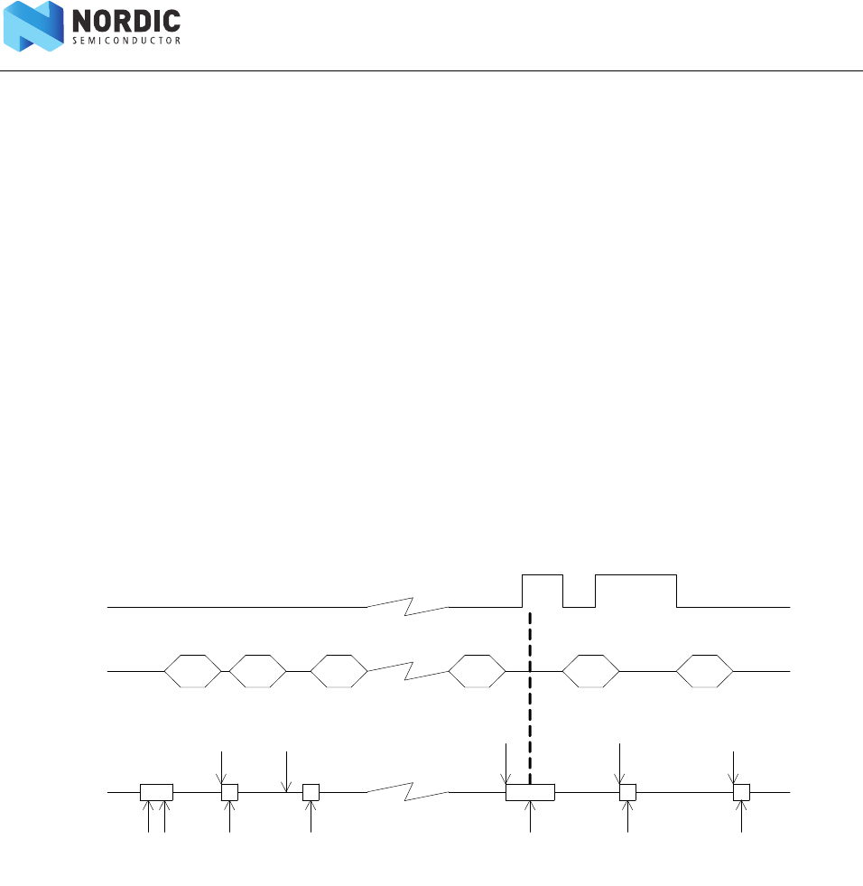
Page 161 of 195
nRF51 Series Reference Manual v2.0 - Universal Asynchronous Receiver/Transmitter (UART)
28.3 Shared resources
The UART shares registers and other resources with other peripherals that have the same ID as the UART.
Therefore, you must disable all peripherals that have the same ID as the UART before the UART can be
configured and used. Disabling a peripheral that has the same ID as the UART will not reset any of the
registers that are shared with the UART. It is therefore important to configure all relevant UART registers
explicitly to ensure that it operates correctly.
See the Instantiation table in Section 4.2 “Instantiation” on page 13 for details on peripherals and their IDs.
28.4 Transmission
A UART transmission sequence is started by triggering the STARTTX task. Bytes are transmitted by writing to
the TXD register. When a byte has been successfully transmitted the UART will generate a TXDRDY event
after which a new byte can be written to the TXD register. A UART transmission sequence is stopped
immediately by triggering the STOPTX task.
If flow control is enabled a transmission will be automatically suspended when CTS is deactivated and
resumed when CTS is activated again, as illustrated in Figure 68. A byte that is in transmission when CTS is
deactivated will be fully transmitted before the transmission is suspended.
Figure 68 UART transmission
28.5 Reception
A UART reception sequence is started by triggering the STARTRX task. The UART receiver chain implements a
FIFO capable of storing six incoming RXD bytes before data is overwritten. Bytes are extracted from this FIFO
by reading the RXD register. When a byte is extracted from the FIFO a new byte pending in the FIFO will be
moved to the RXD register. The UART will generate an RXDRDY event every time a new byte is moved to the
RXD register.
When flow control is enabled, the UART will deactivate the RTS signal when there is only space for four more
bytes in the receiver FIFO. The counterpart transmitter is therefore able to send up to four bytes after the RTS
signal is deactivated before data is being overwritten. To prevent overwriting data in the FIFO, the
counterpart UART transmitter must therefore make sure to stop transmitting data within four bytes after the
RTS line is deactivated.
CTSTXD
STARTTX
TX D = 0
TXDRDY
Lifeline
TX D = 1
TXDRDY
TXD = N
TXDRDY
1 5 62
TXDRDY
TX D = 2
3
0 1 2 N- 1
TXD = N-1
5
TXDRDY
N- 2 N
STOPTX
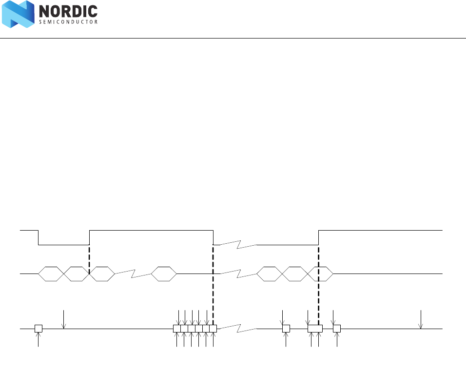
Page 162 of 195
nRF51 Series Reference Manual v2.0 - Universal Asynchronous Receiver/Transmitter (UART)
The RTS signal will first be activated again when the FIFO has been emptied, that is, when all bytes in the
FIFO have been read by the CPU, see Figure 69.
The RTS signal will also be deactivated when the receiver is stopped through the STOPRX task as illustrated
in Figure 69. The UART will be able to receive up to four bytes if they are sent immediately after the RTS
signal has been deactivated. This is possible because the UART is, even after the STOPRX task is triggered,
able to receive bytes for an extended period equal to the time it takes to send four bytes on the configured
baud rate. The UART will generate a receiver timeout event (RXTO) when this period has elapsed.
To prevent loss of incoming data the RXD register must only be read once following every RXDRDY event.
If there is more than one byte available in the FIFO, RXDRDY event will be triggered immediately when the
RXD register is read. To ensure that you have control of any new RXDRDY event arriving you must clear the
EVENT before you read the RXD register.
Figure 69 UART reception.
As indicated in occurrence 2 in Figure 69, the RXDRDY event associated with byte B is generated first after
byte A has been extracted from RXD.
28.6 Error conditions
An ERROR event, in the form of a framing error, will be generated if a valid stop bit is not detected in a frame.
Another ERROR event, in the form of a break condition, will be generated if the RXD line is held active low for
longer than the length of a data frame. Effectively, a framing error is always generated before a break
condition occurs.
28.7 Using the UART without flow control
If flow control is not enabled the interface will behave as if the CTS and RTS lines are kept active all the time.
28.8 Parity configuration
When parity is enabled, the parity will be generated automatically from the even parity of TXD and RXD for
transmission and reception respectively.
RTSRX D
STARTRX
RXDRDY
Lifeline
A = R XD
RXDRDY
1 2
B = R XD
3
A B C
RXDRDY
M-2 M-1
RXDRDY
M-2 = RXD
5
RXDRDY
M-1 = RXD
6
M
RXDRDY
M = RXD
7
STOP RX
C = RXD
4
RXDRDY
D = RXD
5
E = R XD
6
RXDRDY
F = RXD
7
RXDRDY
F
RXTO

Page 163 of 195
nRF51 Series Reference Manual v2.0 - Universal Asynchronous Receiver/Transmitter (UART)
28.9 Registers
Table 41 Register overview
28.9.1 RXD
Register Offset Description
TASKS
STARTRX 0x000 Start UART receiver
STOPRX 0x004 Stop UART receiver
STARTTX 0x008 Start UART transmitter
STOPTX 0x00C Stop UART transmitter
EVENTS
RXDRDY 0x108 Data received in RXD
TXDRDY 0x11C Data sent from TXD
ERROR 0x124 Error detected
RXTO 0x144 Receiver timeout
REGISTERS
INTENSET 0x304 Interrupt enable set register
INTENCLR 0x308 Interrupt enable clear register
ERRORSRC 0x480 Error source
ENABLE 0x500 Enable UART
PSELRTS 0x508 Pin select for RTS
PSELTXD 0x50C Pin select for TXD
PSELCTS 0x510 Pin select for CTS
PSELRXD 0x514 Pin select for RXD
RXD 0x518 RXD register
TXD 0x51C TXD register
BAUDRATE 0x524 Baud rate
CONFIG 0x56C Configuration of parity and hardware flow control
Bit number 31 30 29 28 27 26 25 24 23 22 21 20 19 18 17 16 15 14 13 12 11 10 9 8 7 6 5 4 3 2 1 0
ID (Field ID) ------------------------AAAAAAAA
Reset value 00000000000000000000000000000000
ID RW Field Value ID Value Description
A R RX data received in previous transfers.

Page 164 of 195
nRF51 Series Reference Manual v2.0 - Universal Asynchronous Receiver/Transmitter (UART)
28.9.2 TXD
28.9.3 ENABLE
28.9.4 PSELRTS
28.9.5 PSELTXD
Bit number 31 30 29 28 27 26 25 24 23 22 21 20 19 18 17 16 15 14 13 12 11 10 9 8 7 6 5 4 3 2 1 0
ID (Field ID) - - - - - - - - - - - - - - - - - - - - - - - - A A A A A A A A
Reset value 0 0 0 0 0 0 0 0 0 0 0 0 0 0 0 0 0 0 0 0 0 0 0 0 0 0 0 0 0 0 0 0
ID RW Field Value ID Value Description
A W TX data to be transferred.
Bit number 31 30 29 28 27 26 25 24 23 22 21 20 19 18 17 16 15 14 13 12 11 10 9 8 7 6 5 4 3 2 1 0
ID (Field ID) 0 0 0 0 0 0 0 0 0 0 0 0 0 0 0 0 0 0 0 0 0 0 0 0 0 0 0 0 0 A A A
Reset value 0 0 0 0 0 0 0 0 0 0 0 0 0 0 0 0 0 0 0 0 0 0 0 0 0 0 0 0 0 0 0 0
ID RW Field Value ID Value Description
A RW Enable or disable UART
DISABLE 0Disable UART
ENABLE 4 Enable UART
Bit number 31 30 29 28 27 26 25 24 23 22 21 20 19 18 17 16 15 14 13 12 11 10 9 8 7 6 5 4 3 2 1 0
ID (Field ID) AAAAAAAAAAAAAAAAAAAAAAAAAAAAAAAA
Reset value 11111111111111111111111111111111
ID RW Field Value ID Value Description
A Pin number configuration for UART RTS signal
RW [0..31] Pin number to route the UART RTS signal to
W 0xFFFFFFFF Disconnect
Bit number 31 30 29 28 27 26 25 24 23 22 21 20 19 18 17 16 15 14 13 12 11 10 9 8 7 6 5 4 3 2 1 0
ID (Field ID) A A A A A A A A A A A A A A A A A A A A A A A A A A A A A A A A
Reset value 1 1 1 1 1 1 1 1 1 1 1 1 1 1 1 1 1 1 1 1 1 1 1 1 1 1 1 1 1 1 1 1
ID RW Field Value ID Value Description
A Pin number configuration for UART TXD signal
RW [0..31] Pin number to route the UART TXD signal to
W 0xFFFFFFFF Disconnect

Page 165 of 195
nRF51 Series Reference Manual v2.0 - Universal Asynchronous Receiver/Transmitter (UART)
28.9.6 PSELCTS
28.9.7 PSELRXD
28.9.8 ERRORSRC
Bit number 31 30 29 28 27 26 25 24 23 22 21 20 19 18 17 16 15 14 13 12 11 10 9 8 7 6 5 4 3 2 1 0
ID (Field ID) A A A A A A A A A A A A A A A A A A A A A A A A A A A A A A A A
Reset value 1 1 1 1 1 1 1 1 1 1 1 1 1 1 1 1 1 1 1 1 1 1 1 1 1 1 1 1 1 1 1 1
ID RW Field Value ID Value Description
A Pin number configuration for UART CTS signal
RW [0..31] Pin number to route the UART CTS signal to
W 0xFFFFFFFF Disconnect
Bit number 31 30 29 28 27 26 25 24 23 22 21 20 19 18 17 16 15 14 13 12 11 10 9 8 7 6 5 4 3 2 1 0
ID (Field ID) AAAAAAAAAAAAAAAAAAAAAAAAAAAAAAAA
Reset value 11111111111111111111111111111111
ID RW Field Value ID Value Description
A Pin number configuration for UART RXD signal
RW [0..31] Pin number to route the UART RXD signal to
W 0xFFFFFFFF Disconnect
Bit number 31 30 29 28 27 26 25 24 23 22 21 20 19 18 17 16 15 14 13 12 11 10 9 8 7 6 5 4 3 2 1 0
ID (Field ID) - - - - - - - - - - - - - - - - - - - - - - - - - - - - D C B A
Reset value 0 0 0 0 0 0 0 0 0 0 0 0 0 0 0 0 0 0 0 0 0 0 0 0 0 0 0 0 0 0 0 0
ID RW Field Value ID Value Description
A OVERRUN Overrun error.
A start bit is received while the previous data still lies in RXD. (Previous data is lost.)
R 0 Not occurred
R1Occurred
W 1 Clear
B.. PARITY .. Parity error.
A character with bad parity is received, if HW parity check is enabled.
C.. FRAMING .. Framing error occurred.
A valid stop bit is not detected on the serial data input after all bits in a character
have been received.
D .. BREAK .. Break condition.
The serial data input is '0' for longer than the length of a data frame. (The data
frame length is 10 bits without parity bit, and 11 bits with parity bit.)

Page 166 of 195
nRF51 Series Reference Manual v2.0 - Universal Asynchronous Receiver/Transmitter (UART)
28.9.9 CONFIG
28.9.10 BAUDRATE
Bit number 31 30 29 28 27 26 25 24 23 22 21 20 19 18 17 16 15 14 13 12 11 10 9 8 7 6 5 4 3 2 1 0
ID (Field ID) -----------------------------BBA
Reset value 00000000000000000000000000000100
ID RW Field Value ID Value Description
A RW HWFC Hardware flow control
0Disabled
1Enabled
BRW PA RIT Y Parity
0x0 Exclude parity bit
0x7 Include parity bit
Bit number 31 30 29 28 27 26 25 24 23 22 21 20 19 18 17 16 15 14 13 12 11 10 9 8 7 6 5 4 3 2 1 0
ID (Field ID) A A A A A A A A A A A A A A A A A A A A A A A A A A A A A A A A
Reset value 0 0 0 0 0 0 0 1 1 0 0 1 1 0 0 0 0 0 0 0 0 0 0 0 0 0 0 0 0 0 0 0
ID RW Field Value ID Value Description
ARW Baud-rate
BAUD1200 0x0004F000 1200 baud
BAUD2400 0x0009D000 2400 baud
BAUD4800 0x0013B000 4800 baud
BAUD9600 0x00275000 9600 baud
BAUD14400 0x003B0000 14400 baud
BAUD19200 0x004EA000 19200 baud
BAUD28800 0x0075F000 28800 baud
BAUD38400 0x009D5000 38400 baud
BAUD57600 0x00EBF000 57600 baud
BAUD76800 0x013A9000 76800 baud
BAUD115200 0x01D7E000 115200 baud
BAUD230400 0x03AFB000 230400 baud
BAUD250000 0x04000000 250000 baud
BAUD460800 0x075F7000 460800 baud
BAUD921600 0X0EBEDFA4 921600 baud
BAUD1M 0x10000000 1 megabaud
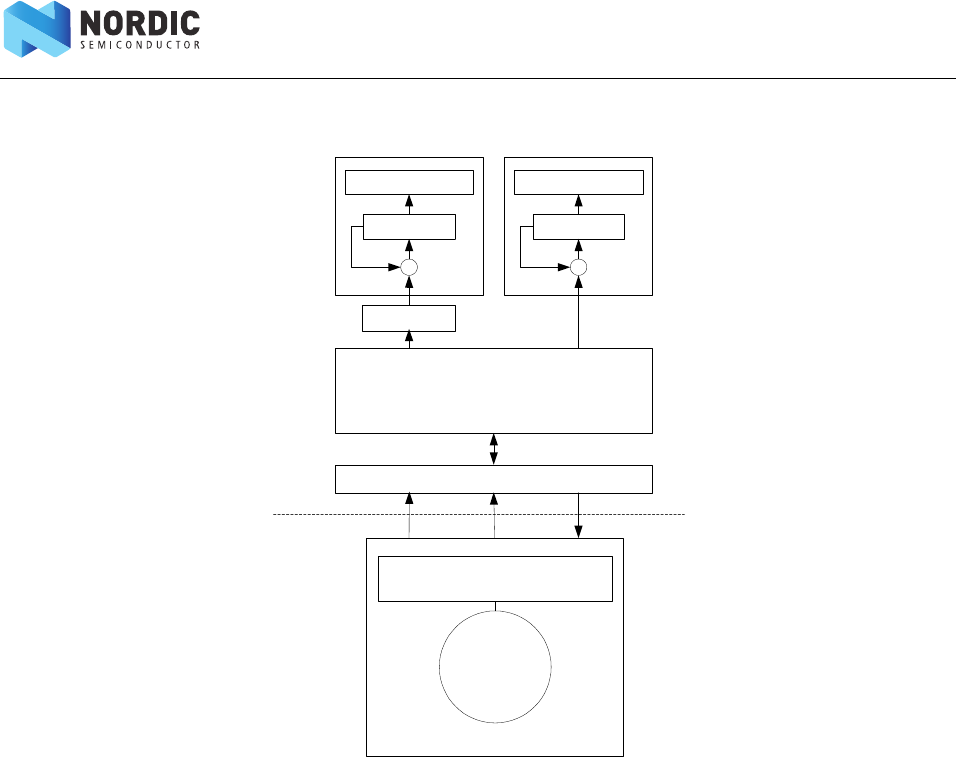
Page 167 of 195
nRF51 Series Reference Manual v2.0 - Quadrature Decoder (QDEC)
29 Quadrature Decoder (QDEC)
Figure 70 Quadrature decoder configuration
29.1 Functional description
The Quadrature Decoder (QDEC) can be used for decoding the output of an off-chip quadrature encoder.
The QDEC provides the following:
• Decoding of digital waveform from off-chip quadrature encoder.
• Sample accumulation eliminating hard real-time requirements to be enforced on
application.
• Optional input debounce filters.
• Optional LED output signal for optical encoders.
29.1.1 Pin configuration
The different signals: Phase A, Phase B, and LED, are mapped to physical pins according to the configuration
specified in the PSELA, PSELB, and PSELLED registers respectively. If a value of 0xFFFFFFFF is specified in any
of these registers, the associated signal will not be connected to any physical pin. The PSELA, PSELB, and
PSELLED registers and their configurations are only used as long as the QDEC is enabled, and retained only
as long as the device is in ON mode.
To secure correct behavior in the QDEC, the pins used by the QDEC must be configured in the GPIO
peripheral as described in Table 42 on page 168 prior to enabling the QDEC. This configuration must be
retained in the GPIO for the selected IOs as long as the QDEC is enabled.
Electrical to mechanical
Mechanical
device
Quadrature decoder
SAMPLE
Quadrature Encoder
IO router
On-chip
Off-chip
ACC
ACCREAD
+
ACCDBL
ACCDBLREAD
+
Phase A Phase B LED

Page 168 of 195
nRF51 Series Reference Manual v2.0 - Quadrature Decoder (QDEC)
Only one peripheral can be assigned to drive a particular GPIO pin at a time, failing to do so may result in
unpredictable behavior.
Table 42 GPIO configuration
29.1.2 Sampling and decoding
The off-chip quadrature encoder is an incremental motion encoder outputting two waveforms; phase A and
phase B. The two output waveforms are always 90 degrees out of phase, meaning that one always changes
level before the other. The direction of movement is indicated by which of these two waveforms that
changes level first. Invalid transitions may occur, that is when the two waveforms switch simultaneously.
This may occur if the wheel rotates too fast relative to the sample rate set for the decoder.
The QDEC decodes the output from the off-chip encoder by sampling the QDEC phase input pins (A and B)
at a fixed rate as specified in the SAMPLEPER register.
When started, the decoder continuously samples the two input waveforms and decodes these by
comparing the current sample pair (n) with the previous sample pair (n-1). The decoding of the sample pairs
is described in Table 43.
Table 43 Quadrature decoder input decoding
QDEC signal QDEC pin Direction Output value
Phase A As specified in PSELA Input Not applicable
Phase B As specified in PSELB Input Not applicable
LED As specified in PSELLED Input Not applicable
Previous sample pair
(n - 1)
Current samples
pair (n) SAMPLE
register
ACC
operation
ACCDBL
operation Description
A B A B
0 0 0 0 0 No change No change No movement
0 1 1 Increment No change Movement in positive direction
1 0 -1 Decrement No change Movement in negative direction
1 1 2 No change Increment Error: Double transition
0 1 0 0 -1 Decrement No change Movement in negative direction
0 1 0 No change No change No movement
1 0 2 No change Increment Error: Double transition
1 1 1 Increment No change Movement in positive direction
1 0 0 0 1 Increment No change Movement in positive direction
0 1 2 No change Increment Error: Double transition
1 0 0 No change No change No movement
1 1 -1 Decrement No change Movement in negative direction
1 1 0 0 2 No change Increment Error: Double transition
0 1 -1Decrement No change Movement in negative direction
1 0 1 Increment No change Movement in positive direction
1 1 0 No change No change No movement

Page 169 of 195
nRF51 Series Reference Manual v2.0 - Quadrature Decoder (QDEC)
29.1.3 LED output
The LED output follows the sample period and the LED is switched on a given period prior to sampling and
switched off immediately after the inputs are sampled. The period the LED is switched on prior to sampling
is given in the LEDPRE register.
The LED output pin polarity is specified in the LEDPOL register.
For using off-chip mechanical encoders not requiring a LED, the LED output can be disabled by writing
0xFFFFFFFF to the PSELLED register. In this case the QDEC will not acquire access to a LED output pin and
the pin can be used for other purposes by the CPU.
29.1.4 Debounce filters
Each of the two phase inputs have digital debounce filters. When enabled, the filter inputs are sampled at a
fixed 1 MHz frequency during the entire sample period (which is specified in the SAMPLEPER register), and
the filters require all of the samples within this sample period to equal before the input signal is accepted
and transferred to the output of the filter.
As a result, only input signal with a steady state longer than twice the period specified in SAMPLEPER are
guaranteed to pass through the filter, and any signal with a steady state shorter than SAMPLEPER will always
be suppressed by the filter. (This is assumed that the frequency during the debounce period never exceeds
500 kHz (as required by the Nyquist theorem when using a 1 MHz sample frequency).
Note: The LED will always be ON when the debounce filters are enabled, as the inputs in this case
will be sampled continuously.
29.1.5 Accumulators
The quadrature decoder contains two the accumulator registers ACC and ACCDBL that accumulates valid
motion sample values and the number of detected invalid samples (double transitions), respectively.
The ACC register will accumulate all valid values (1/-1) written to the SAMPLE register. This can be useful for
preventing hard real-time requirements from being enforced on the application. When using the ACC
register the application does not need to read every single sample from the SAMPLE register, but can
instead fetch the ACC register whenever it fits the application. The ACC register will always hold the relative
movement of the external mechanical device since the previous clearing of the ACC register. Sample values
indicating a double transition (2) will not be accumulated in the ACC register.
An ACCOF event will be generated if the ACC receives a SAMPLE value that would cause the register to
overflow or underflow. Any SAMPLE value that would cause the an ACC overflow or underflow will be
discarded, but any samples not causing the ACC to overflow or underflow will still be accepted.
The accumulator ACCDBL accumulates the number of detected double transitions since the previous
clearing of the ACCDBL register.
The ACC and ACCDBL registers can be cleared by the READCLRACC and subsequently read using the
ACCREAD and ACCDBLREAD registers.

Page 170 of 195
nRF51 Series Reference Manual v2.0 - Quadrature Decoder (QDEC)
29.1.6 Output/input pins
The QDEC uses a 3 pin interface to the off-chip quadrature encoder.
These pins will be acquired when the QDEC is enabled in the ENABLE register. The pins acquired by the
QDEC cannot be written by the CPU, but they can still be read by the CPU.
The pin numbers to be used for the QDEC are selected using the PSELn registers.
29.2 Registers
Register Offset Description
TASKS
START 0x000 Task starting the quadrature decoder. When started, the SAMPLE register will be
continuously updated at the rate given in the SAMPLEPER register.
STOP 0x004 Task stopping the quadrature decoder.
READCLRACC 0x008 Task transferring the content of ACC to ACCREAD and the content of ACCDBL to
ACCDBLREAD, and then clearing the ACC and ACCDBL registers. These read-and-
clear operations will be done automatically.
EVENTS
SAMPLERDY 0x100 Event being generated for every new sample value written to the SAMPLE register.
REPORTRDY 0X104 Event being generated when REPORTPER number of samples has been accumulated
in the ACC register and the content of the ACC register does not equal 0. (Thus, this
event is only generated if a motion is detected since the previous clearing of the ACC
register).
ACCOF 0X108 ACC or ACCDBL register overflow.
REGISTERS
SHORTS 0x200 Shortcut register.
INTENSET 0x304 Interrupt enable set register.
INTENCLR 0x308 Interrupt enable clear register.
ENABLE 0x500 ADC enable.
LEDPOL 0x504 ADC configuration.
SAMPLEPER 0x508 ADC conversion result.
SAMPLE 0X50C Motion sample value.
REPORTPER 0X510 Number of samples to be taken before a REPORTRDY event is generated.
ACC 0X514 Register accumulating the valid transitions.
ACCREAD 0X518 Snapshot of the ACC register updated by the READCLRACC task.
PSELLED 0X51C GPIO pin number to be used as LED output.
PSELA 0X520 GPIO pin number to be used as Phase A input.
PSELB 0X524 GPIO pin number to be used as Phase B input.
DBFEN 0X528 Enable input debounce filters.
LEDPRE 0X540 Time period the LED is switched ON prior to sampling.
ACCDBL 0X544 Register accumulating the number of detected double transitions.
ACCDBLREAD 0X548 Snapshot of the ACCDBL.

Page 171 of 195
nRF51 Series Reference Manual v2.0 - Quadrature Decoder (QDEC)
29.2.1 Shorts
29.2.2 ENABLE
29.2.3 LEDPOL
Bit number 31 30 29 28 27 26 25 24 23 22 21 20 19 18 17 16 15 14 13 12 11 10 9 8 7 6 5 4 3 2 1 0
ID (Field ID) ------------------------------BA
Reset value 00000000000000000000000000000000
ID RW Field Value ID Value Description
ARW REPORTRDY_
READCLRACC Disable
Enable
0
1
Short REPORTRDY event to READCLRACC task.
BRW SAMPLERDY_
STOP Disable
Enable
0
1
Short SAMPLERDY event to STOP task.
Bit number 31 30 29 28 27 26 25 24 23 22 21 20 19 18 17 16 15 14 13 12 11 10 9 8 7 6 5 4 3 2 1 0
ID (Field ID) - - - - - - - - - - - - - - - - - - - - - - - - - - - - - - - A
Reset value 0 0 0 0 0 0 0 0 0 0 0 0 0 0 0 0 0 0 0 0 0 0 0 0 0 0 0 0 0 0 0 0
ID RW Field Value ID Value Description
A RW VAL Enable the quadrature decoder. When enabled, the decoder pins will be active.
When disabled, the quadrature decoder pins are not active and can be used as
GPIO.
DISABLE 0
ENABLE 1
Bit number 31 30 29 28 27 26 25 24 23 22 21 20 19 18 17 16 15 14 13 12 11 10 9 8 7 6 5 4 3 2 1 0
ID (Field ID) -------------------------------A
Reset value 00000000000000000000000000000000
ID RW Field Value ID Value Description
ARW LED output polarity.
ACTIVELOW 0LED active on output pin low.
ACTIVEHIGH 1 LED active on output pin high.

Page 172 of 195
nRF51 Series Reference Manual v2.0 - Quadrature Decoder (QDEC)
29.2.4 SAMPLEPER
29.2.5 SAMPLE
Bit number 31 30 29 28 27 26 25 24 23 22 21 20 19 18 17 16 15 14 13 12 11 10 9 8 7 6 5 4 3 2 1 0
ID (Field ID) - - - - - - - - - - - - - - - - - - - - - - - - - - - - - A A A
Reset value 0 0 0 0 0 0 0 0 0 0 0 0 0 0 0 0 0 0 0 0 0 0 0 0 0 0 0 0 0 0 0 0
ID RW Field Value ID Value Description
A RW VAL Sample period. The SAMPLE register will be updated for every new sample.
128_US 0128 s
256_US 1 256 s
512_US 2512 s
1024_US 3 1024 s
2048_US 42048 s
4096_US 5 4096 s
8192_US 68192 s
16384_US 7 16384 s
Bit number 31 30 29 28 27 26 25 24 23 22 21 20 19 18 17 16 15 14 13 12 11 10 9 8 7 6 5 4 3 2 1 0
ID (Field ID) A A A A A A A A A A A A A A A A A A A A A A A A A A A A A A A A
Reset value 0 0 0 0 0 0 0 0 0 0 0 0 0 0 0 0 0 0 0 0 0 0 0 0 0 0 0 0 0 0 0 0
ID RW Field Value ID Value Description
A R (--1..2) Last motion sample.
The value is a 2’s complement value, and the sign gives the direction of the
motion.
The value ‘2’ indicates a double transition.

Page 173 of 195
nRF51 Series Reference Manual v2.0 - Quadrature Decoder (QDEC)
29.2.6 REPORTPER
29.2.7 ACC
Bit number 31 30 29 28 27 26 25 24 23 22 21 20 19 18 17 16 15 14 13 12 11 10 9 8 7 6 5 4 3 2 1 0
ID (Field ID) - - - - - - - - - - - - - - - - - - - - - - - - - - - - - A A A
Reset value 0 0 0 0 0 0 0 0 0 0 0 0 0 0 0 0 0 0 0 0 0 0 0 0 0 0 0 0 0 0 0 0
ID RW Field Value ID Value Description
A RW VAL Specifies the number of samples to be accumulated in the ACC register before
the REPORTRDY event can be generated.
The report period in s is given as:
RPUS = SP * RP
Where
RPUS is the report period in [s/report
SP is the sample period in [s/sample] specified in SAMPLEPER
RP is the report period in [samples/report] specified in REPORTPER
10_SMPL 010 samples/report
40_SMPL 1 40 samples/report
80_SMPL 280 samples/report
120_SMPL 3 120 samples/report
160_SMPL 4160 samples/report
200_SMPL 5 200 samples/report
240_SMPL 6240 samples/report
280_SMPL 7 280 samples/report
Bit number 31 30 29 28 27 26 25 24 23 22 21 20 19 18 17 16 15 14 13 12 11 10 9 8 7 6 5 4 3 2 1 0
ID (Field ID) A A A A A A A A A A A A A A A A A A A A A A A A A A A A A A A A
Reset value 0 0 0 0 0 0 0 0 0 0 0 0 0 0 0 0 0 0 0 0 0 0 0 0 0 0 0 0 0 0 0 0
ID RW Field Value ID Value Description
A R (-1024..1023) Register accumulating all valid samples (not double transition) read from the
RENC (in the SAMPLE register). Double transitions (SAMPLE = 2) will not be
accumulated in this register.
The value is a 32 bit 2’s complement value.
If a sample that would cause this register to overflow or underflow is received, the
sample will be ignored and an overflow event (ACCOF) will be generated.
The ACC register is cleared by triggering the READCLRACC task.

Page 174 of 195
nRF51 Series Reference Manual v2.0 - Quadrature Decoder (QDEC)
29.2.8 ACCREAD
29.2.9 PSELLED
29.2.10 PSELA
29.2.11 PSELB
29.2.12 LEDPRE
Bit number 31 30 29 28 27 26 25 24 23 22 21 20 19 18 17 16 15 14 13 12 11 10 9 8 7 6 5 4 3 2 1 0
ID (Field ID) A A A A A A A A A A A A A A A A A A A A A A A A A A A A A A A A
Reset value 0 0 0 0 0 0 0 0 0 0 0 0 0 0 0 0 0 0 0 0 0 0 0 0 0 0 0 0 0 0 0 0
ID RW Field Value ID Value Description
A R (-1024..1023) Snapshot of the ACC register.
The ACCREAD register is updated when the READCLRACC task is triggered,
Bit number 31 30 29 28 27 26 25 24 23 22 21 20 19 18 17 16 15 14 13 12 11 10 9 8 7 6 5 4 3 2 1 0
ID (Field ID) A A A A AAAAAAAAAAAAAAAAAAAAAAAAAAAA
Reset value 1 1 1 1 1111111111111111111111111111
ID RW Field Value ID Value Description
A RW (0..31) GPIO pin number to be used as LED output. Writing the value 0xFFFFFFFF will
disable this output.
Bit number 31 30 29 28 27 26 25 24 23 22 21 20 19 18 17 16 15 14 13 12 11 10 9 8 7 6 5 4 3 2 1 0
ID (Field ID) A A A A A A A A A A A A A A A A A A A A A A A A A A A A A A A A
Reset value 1 1 1 1 1 1 1 1 1 1 1 1 1 1 1 1 1 1 1 1 1 1 1 1 1 1 1 1 1 1 1 1
ID RW Field Value
ID Value Description
A RW (0..31) GPIO pin number to be used as Phase A input. Writing the value 0xFFFFFFFF will
disable this input.
Bit number 31 30 29 28 27 26 25 24 23 22 21 20 19 18 17 16 15 14 13 12 11 10 9 8 7 6 5 4 3 2 1 0
ID (Field ID) A A A A A A A A A A A A A A A A A A A A A A A A A A A A A A A A
Reset value 1 1 1 1 1 1 1 1 1 1 1 1 1 1 1 1 1 1 1 1 1 1 1 1 1 1 1 1 1 1 1 1
ID RW Field Value ID Value Description
A RW (0..31) GPIO pin number to be used as Phase B input. Writing the value 0xFFFFFFFF will
disable this input.
Bit number 31 30 29 28 27 26 25 24 23 22 21 20 19 18 17 16 15 14 13 12 11 10 9 8 7 6 5 4 3 2 1 0
ID (Field ID) - - - - - - - - - - - - - - - - - - - - - - - A A A A A A A A A
Reset value 0 0 0 0 0 0 0 0 0 0 0 0 0 0 0 0 0 0 0 0 0 0 0 0 0 0 0 0 0 0 0 0
ID RW Field Value ID Value Description
A RW (0..511) Period in s the LED is switched on prior to sampling.

Page 175 of 195
nRF51 Series Reference Manual v2.0 - Quadrature Decoder (QDEC)
29.2.13 DBFEN
29.2.14 ACCDBL
29.2.15 ACCDBLREAD
Bit number 31 30 29 28 27 26 25 24 23 22 21 20 19 18 17 16 15 14 13 12 11 10 9 8 7 6 5 4 3 2 1 0
ID (Field ID) - - - - - - - - - - - - - - - - - - - - - - - - - - - - - - - A
Reset value 0 0 0 0 0 0 0 0 0 0 0 0 0 0 0 0 0 0 0 0 0 0 0 0 0 0 0 0 0 0 0 0
ID RW Field Value ID Value Description
A RW Enable input debounce filters.
0Disable
1Enable
Bit number 31 30 29 28 27 26 25 24 23 22 21 20 19 18 17 16 15 14 13 12 11 10 9 8 7 6 5 4 3 2 1 0
ID (Field ID) - - - - - - - - - - - - - - - - - - - - - - - - - - - - A A A A
Reset value 0 0 0 0 0 0 0 0 0 0 0 0 0 0 0 0 0 0 0 0 0 0 0 0 0 0 0 0 0 0 0 0
ID RW Field Value ID Value Description
A R (0..15) Register accumulating the number of detected double or illegal transitions.
(SAMPLE = 2).
When this register has reached its maximum value the accumulation of double /
illegal transitions will stop.
An overflow event (ACCOF) will be generated if any double or illegal transitions
are detected after the maximum or minimum value was reached.
This field is cleared by triggering the READCLRACC task.
Bit number 31 30 29 28 27 26 25 24 23 22 21 20 19 18 17 16 15 14 13 12 11 10 9 8 7 6 5 4 3 2 1 0
ID (Field ID) - - - - - - - - - - - - - - - - - - - - - - - - - - - - A A A A
Reset value 0 0 0 0 0 0 0 0 0 0 0 0 0 0 0 0 0 0 0 0 0 0 0 0 0 0 0 0 0 0 0 0
ID RW Field Value ID Value Description
A R (0..15) Snapshot of the ACCDBL register.
This field is updated when the READCLRACC task is triggered.
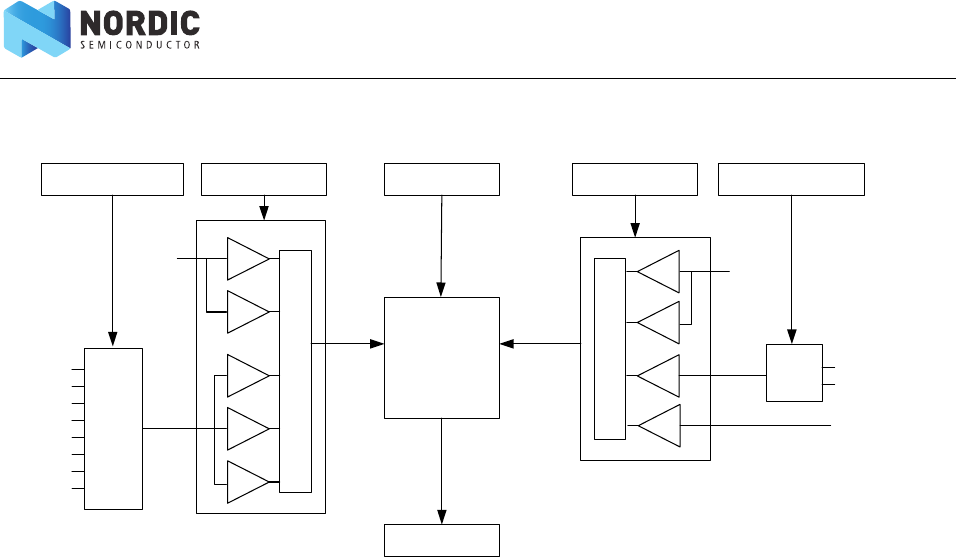
Page 176 of 195
nRF51 Series Reference Manual v2.0 - Analog to Digital Converter (ADC)
30 Analog to Digital Converter (ADC)
Figure 71 Analog to Digital converter
30.1 Functional description
30.1.1 Configuration
All parameters such as input selection, reference selection, resolution, pre-scaling etc. are configured using
the CONFIG register.
Note: It is not allowed to configure the ADC during an on-going ADC conversion (ADC busy).
30.1.2 Usage
An ADC conversion is started by using the START task, either by writing the task register directly from the
CPU or by triggering the task through the PPI.
During sampling the ADC will enter a busy state. The ADC busy/ready state can be monitored via the BUSY
register.
When the ADC conversion is completed, an END event will be generated and the result of the conversion
can be read from the RESULT register.
When the ADC conversion is completed, the ADC analog electronics power down to save power.
30.1.3 One-shot / continuous operation
The ADC itself only supports one-shot operation, this means every single conversion has to be explicitly
started using the START task.
However, continuous ADC operation can be achieved by continuously triggering the START task from, for
example, a timer through the PPI.
1/3
2/3
1/3
2/3
1
M
U
X
VDD
Reference
AIN2
AIN3
AIN4
AIN5
AIN0
AIN1
AIN6
AIN7 ADC
CONFIG.INPSEL
CONFIG.PSEL CONFIG.RES
SAMPLE
MUX
Input
1/3
1/2
M
U
X
VDD
1MUX AREF0
AREF1
CONFIG.EXTREFSEL
CONFIG.REFSEL
VBG
1

Page 177 of 195
nRF51 Series Reference Manual v2.0 - Analog to Digital Converter (ADC)
30.1.4 Pin configuration
The user can use the PSEL register to select one of the analog input pins, AIN0 through AIN7, as input for the
ADC. See the device product specification for more information about which analog pins are available on a
particular device. The selected analog pin will be acquired by the ADC when it is enabled through the
ENABLE register, see Chapter 13 “GPIO” on page 58 for more information on how analog pins are selected.
30.1.5 Shared resources
The ADC shares registers and other resources with peripherals that have the same ID as the ADC. The user
must therefore disable all peripherals that have the same ID as the ADC before the ADC can be configured
and used. The ADC is using the same analog pins as the LPCOMP. The LPCOMP must therefore be disabled
before the ADC can be enabled. It is important to configure all relevant ADC registers explicitly to secure
that it operates correctly.
The Instantiation table in Section 4.2 “Instantiation” on page 13 shows which peripherals have the same ID
as the ADC.
30.2 Registers
Table 44 Register overview
30.2.1 BUSY
Register Offset Description
TASKS
START 0x000 Start a new ADC conversion.
STOP 0x004 Stop ADC.
EVENTS
END 0x100 An ADC conversion is completed.
REGISTERS
INTENSET 0x304 Interrupt enable set register.
INTENCLR 0x308 Interrupt enable clear register.
BUSY 0x400 ADC busy (conversion in progress).
ENABLE 0x500 Enable ADC. When enabled, the ADC will acquire access to the analog input pins
specified in the CONFIG register.
CONFIG 0x504 ADC configuration.
RESULT 0x508 Result of the previous ADC conversion.
Bit number 31 30 29 28 27 26 25 24 23 22 21 20 19 18 17 16 15 14 13 12 11 10 9 8 7 6 5 4 3 2 1 0
ID (Field ID) - - - - - - - - - - - - - - - - - - - - - - - - - - - - - - - A
Reset value 0 0 0 0 0 0 0 0 0 0 0 0 0 0 0 0 0 0 0 0 0 0 0 0 0 0 0 0 0 0 0 0
ID RW Field Value ID Value Description
AR
0ADC is ready. No ongoing conversion.
1 ADC is busy. Conversion in progress.

Page 178 of 195
nRF51 Series Reference Manual v2.0 - Analog to Digital Converter (ADC)
30.2.2 ENABLE
Bit number 31 30 29 28 27 26 25 24 23 22 21 20 19 18 17 16 15 14 13 12 11 10 9 8 7 6 5 4 3 2 1 0
ID (Field ID) -------- ----------------------AA
Reset value 00000000 000000000000000000000000
ID RW Field Value ID Value Description
ARW VAL
0ADC disabled.
1ADC enabled.

Page 179 of 195
nRF51 Series Reference Manual v2.0 - Analog to Digital Converter (ADC)
30.2.3 CONFIG
Bit number 31 30 29 28 27 26 25 24 23 22 21 20 19 18 17 16 15 14 13 12 11 10 9 8 7 6 5 4 3 2 1 0
ID (Field ID) - - - - - - - - - - - - - - E E D D D D D D D D - C C B B B A A
Reset value 0 0 0 0 0 0 0 0 0 0 0 0 0 0 0 0 0 0 0 0 0 0 0 0 0 0 0 0 0 0 0 0
ID RW Field Value ID Value Description
ARWRES ADC resolution.
8_BIT 08 bit
9_BIT 1 9 bit
10_BIT 210 bit
B RW INPSEL ADC input selection.
AIN_NO_
PS
0Analog input pin specified by CONFIG.PSEL with no prescaling.
AIN_
2_3_PS
1 Analog input pin specified by CONFIG. PSEL with 2/3 prescaling.
AIN_
1_3_PS
2Analog input pin specified by CONFIG. PSEL with 1/3 prescaling.
VDD
2_3_PS
5VDD with 2/3 prescaling.
VDD
1_3_PS
6VDD with 1/3 prescaling.
C RW REFSEL ADC reference selection
VBG 0Use internal 1.2 V band gap reference.
EXT 1 Use external reference specified by CONCFIG EXTREFSEL.
VDD_1_2
_PS
2Use VDD with 1/2 prescaling. (Only applicable when VDD is in the range 1.7V –
2.6V).
VDD_1_3
_PS
3 Use VDD with 1/3 prescaling. (Only applicable when VDD is in the range 2.5V –
3.6V).
DRW PSEL Select pin to be used as ADC input pin.
DISABLE 0 Analog input pins disabled.
AIN0 1Use AIN0 as analog input.
AIN1 2 Use AIN1 as analog input.
AIN2 4Use AIN2 as analog input.
AIN3 8 Use AIN3 as analog input.
AIN4 16 Use AIN4 as analog input.
AIN5 32 Use AIN5 as analog input.
AIN6 64 Use AIN6 as analog input.
AIN7 128 Use AIN7 as analog input.
ERW EXTREFSEL External reference pin selection.
NONE 0 Analog reference inputs disabled.
AREF0 1Use AREF0 as analog reference.
AREF1 2 Use AREF1 as analog reference.

Page 180 of 195
nRF51 Series Reference Manual v2.0 - Analog to Digital Converter (ADC)
30.2.4 RESULT
Bit number 31 30 29 28 27 26 25 24 23 22 21 20 19 18 17 16 15 14 13 12 11 10 9 8 7 6 5 4 3 2 1 0
ID (Field ID) -------- --------------AAAAAAAAAA
Reset value 00000000 000000000000000000000000
ID RW Field Value ID Value Description
A R [0..1023] Result of the previous ADC conversion. The value is updated for every completed
ADC conversion. The result value is relative to the selected ADC reference input. If
the sampled analog input signal is equal to or greater than the ADC reference
signal, the result value will be set to the maximum (limited by the selected ADC bit
width). The value is right justified (LSB of sample value always on register bit 0).
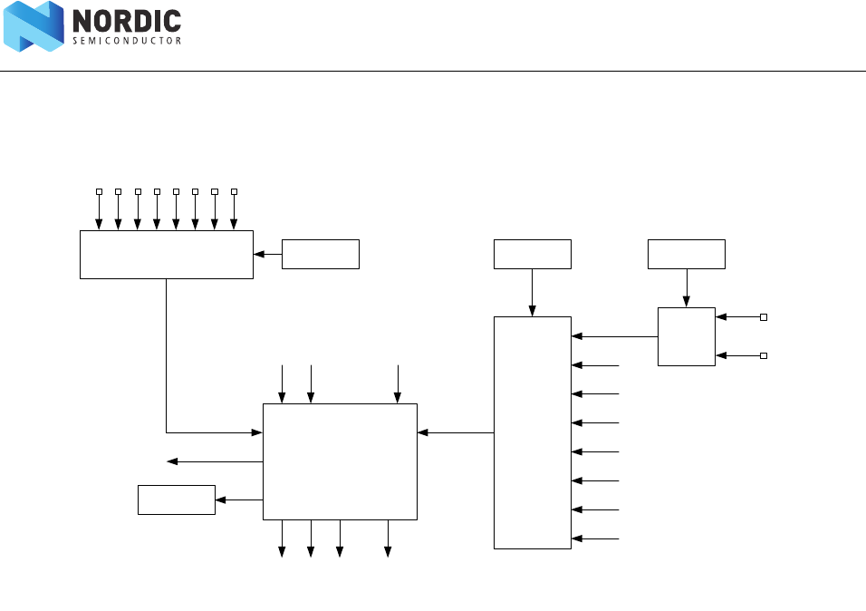
Page 181 of 195
nRF51 Series Reference Manual v2.0 - Low Power Comparator (LPCOMP)
31 Low Power Comparator (LPCOMP)
Figure 72 Low power comparator
31.1 Functional description
The low power comparator (LPCOMP) compares an input voltage (VIN+), which comes from an analog input
pin selected through the PSEL register against a reference voltage (VIN-) selected through the REFSEL and
EXTREFSEL registers.
The PSEL, REFSEL, and EXTREFSEL registers must be configured before the LPCOMP is enabled through the
ENABLE register.
The LPCOMP is started by triggering the START task. After a start-up time of tLPCOMPSTARTUP the LPCOMP will
generate a READY event to indicate that the comparator is ready to use and the output of the LPCOMP is
correct. After the READY event is generated, the LPCOMP will generate events every time VIN+ crosses VIN-,
that is, every time VIN+ rises above VIN- (upward crossing) and every time VIN+ falls below VIN- (downward
crossing), see Figure 72. The LPCOMP is stopped by triggering the STOP task.
An upward crossing will generate an UP event and a downward crossing will generate a DOWN event. The
CROSS event will be generated every time there is a crossing, independent of direction.
LPCOMP will be operational in both System ON and System OFF mode when it is enabled through the
ENABLE register, see Chapter 11 “Power management (POWER)” on page 40 for more information about
power modes. All LPCOMP registers including the ENABLE register are classified as retained registers when
the LPCOMP is enabled. However, when the device wakes up from System OFF, all LPCOMP registers will be
reset.
The LPCOMP can wake up the system from System OFF by asserting the ANADETECT signal. The
ANADETECT signal can be derived from any of the event sources that generate the UP, DOWN, and CROSS
events. In case of wakeup from System OFF, no events will be generated, only the ANADETECT signal. See
the ANADETECT register Section 31.4.7 “ANADETECT” on page 185 for more information on how to
REFSEL
Comparator
core
START
STOP
MUX
VIN-
ANADETECT
(signal to POWER module )
MUX
AIN7
AIN6
AIN5
AIN4
AIN3
AIN2
AIN1
AIN0
VIN+
PSEL
AREF
AVDD*1/8
AVDD*2/8
AVDD*3/8
AVDD*4/8
AVDD*5/8
AVDD*6/8
AVDD*7/8
MUX
EXTREFSEL
UP
CROSS
DO WN
AREF1
AREF0
RESULT
SAMPLE
+-
READY

Page 182 of 195
nRF51 Series Reference Manual v2.0 - Low Power Comparator (LPCOMP)
configure the ANADETECT signal.
The immediate value of the LPCOMP can be sampled to the RESULT register by triggering the SAMPLE task.
See the Section 11.2.1 “RESETREAS” on page 50 on the RESETREAS register in the POWER module for more
information on how to detect a wakeup from LPCOMP.
31.2 Pin configuration
You can use the PSEL register to select one of the analog input pins, AIN0 through AIN7, as analog input pin
for the LPCOMP, see Figure 72 on page 181. Similarly, you can use the EXTREFSEL register to select one of the
analog reference input pins, AREF0 and AREF1, as input for AREF in case AREF is selected in REFSEL. The
selected analog pins will be acquired by the LPCOMP when it is enabled through the ENABLE register. See
the product specification for more information about which analog pins are available on a particular device.
31.3 Shared resources
The LPCOMP shares registers and other resources with peripherals that have the same ID as the LPCOMP.
You must disable all peripherals that have the same ID as the LPCOMP before the LPCOMP can be
configured and used. Disabling a peripheral that has the same ID as the LPCOMP will not reset any of the
registers that are shared with the LPCOMP. Therefore, it is important to configure all relevant LPCOMP
registers explicitly to secure that it operates correctly.
See the Instantiation table in Section 4.2 “Instantiation” on page 13 for details on peripherals and their IDs.
Note: The LPCOMP is using the same analog pins as the ADC. The ADC must be disabled before the
LPCOMP can be enabled.

Page 183 of 195
nRF51 Series Reference Manual v2.0 - Low Power Comparator (LPCOMP)
31.4 Registers
Table 45 Register overview
31.4.1 SHORTS
Register Offset Description
TASKS
START 0x000 Start comparator.
STOP 0x004 Stop comparator.
SAMPLE 0x008 Sample comparator value.
EVENTS
READY 0x100 LPCOMP is ready and output is valid.
DOWN 0x104 Downward crossing.
UP 0x108 Upward crossing.
CROSS 0x10C Downward or upward crossing.
REGISTERS
SHORTS 0x200 Shortcuts for LPCOMP.
INTENSET 0x304 Interrupt enable set register.
INTENCLR 0x308 Interrupt enable clear register.
RESULT 0x400 Compare result.
ENABLE 0x500 Enable LPCOMP.
PSEL 0x504 Input pin select.
REFSEL 0x508 Reference select.
EXTREFSEL 0x50C External reference select.
ANADETECT 0x520 Analog detect configuration.
Bit number 31 30 29 28 27 26 25 24 23 22 21 20 19 18 17 16 15 14 13 12 11 10 9 8 7 6 5 4 3 2 1 0
ID (Field ID) -------- -------------------EDCBA
Reset value 00000000 000000000000000000000000
ID RW Field Value ID Value Description
ARW READY_SAMPLE
0
1
Enable or disable shortcut between READY event and SAMPLE task.
Disable shortcut.
Enable shortcut.
BRW READY_STOP
0
1
Enable or disable shortcut between READY event and STOP task.
Disable shortcut.
Enable shortcut.
C RW DOWN_STOP
0
1
Enable or disable shortcut between DOWN event and STOP task.
Disable shortcut.
Enable shortcut.
DRW UP_STOP
0
1
Enable or disable shortcut between UP event and STOP task.
Disable shortcut.
Enable shortcut.
E RW CROSS_STOP
0
1
Enable or disable shortcut between CROSS event and STOP task.
Disable shortcut.
Enable shortcut.

Page 184 of 195
nRF51 Series Reference Manual v2.0 - Low Power Comparator (LPCOMP)
31.4.2 ENABLE
31.4.3 RESULT
31.4.4 PSEL
Bit number 31 30 29 28 27 26 25 24 23 22 21 20 19 18 17 16 15 14 13 12 11 10 9 8 7 6 5 4 3 2 1 0
ID (Field ID) -------- ----------------------AA
Reset value 00000000 000000000000000000000000
ID RW Field Value ID Value Description
ARW
0
1
Enable or disable LPCOMP.
Disable LPCOMP.
Enable LPCOMP.
Bit number 31 30 29 28 27 26 25 24 23 22 21 20 19 18 17 16 15 14 13 12 11 10 9 8 7 6 5 4 3 2 1 0
ID (Field ID) -------- -----------------------A
Reset value 00000000 000000000000000000000000
ID RW Field Value ID Value Description
AR
BELOW
ABOVE
0
1
Result of last compare. Decision point SAMPLE task.
Input voltage is below the reference threshold. (VIN+ < VIN-)
Input voltage is above the reference threshold. (VIN+ > VIN-)
Bit number 31 30 29 28 27 26 25 24 23 22 21 20 19 18 17 16 15 14 13 12 11 10 9 8 7 6 5 4 3 2 1 0
ID (Field ID) -------- ---------------------AAA
Reset value 00000000 000000000000000000000000
ID RW Field Value ID Value Description
A RW Analog pin select.
AIN0 0AIN0 selected as analog input.
AIN1 1 AIN1 selected as analog input.
AIN2 2AIN2 selected as analog input.
AIN3 3 AIN3 selected as analog input.
AIN4 4AIN4 selected as analog input.
AIN5 5 AIN5 selected as analog input.
AIN6 6AIN6 selected as analog input.
AIN7 7 AIN7 selected as analog input.

Page 185 of 195
nRF51 Series Reference Manual v2.0 - Low Power Comparator (LPCOMP)
31.4.5 REFSEL
31.4.6 EXTREFSEL
31.4.7 ANADETECT
Bit number 31 30 29 28 27 26 25 24 23 22 21 20 19 18 17 16 15 14 13 12 11 10 9 8 7 6 5 4 3 2 1 0
ID (Field ID) -------- ---------------------AAA
Reset value 00000000 000000000000000000000000
ID RW Field Value ID Value Description
A RW Reference select.
AVDD_1_8 0AVDD * 1/8 selected as reference.
AVDD_2_8 1 AVDD * 2/8 selected as reference.
AVDD_3_8 2AVDD * 3/8 selected as reference.
AVDD_4_8 3 AVDD * 4/8 selected as reference.
AVDD_5_8 4AVDD * 5/8 selected as reference.
AVDD_6_8 5 AVDD * 6/8 selected as reference.
AVDD_7_8 6AVDD * 7/8 selected as reference.
AREF 7 External analog reference selected.
Bit number 31 30 29 28 27 26 25 24 23 22 21 20 19 18 17 16 15 14 13 12 11 10 9 8 7 6 5 4 3 2 1 0
ID (Field ID) -------- -----------------------A
Reset value 00000000 000000000000000000000000
ID RW Field Value ID Value Description
ARW
AREF0
AREF1
0
1
External analog reference select.
Use AREF0 as external analog reference.
Use AREF1 as external analog reference.
Bit number 31 30 29 28 27 26 25 24 23 22 21 20 19 18 17 16 15 14 13 12 11 10 9 8 7 6 5 4 3 2 1 0
ID (Field ID) -------- ----------------------AA
Reset value 00000000 000000000000000000000000
ID RW Field Value ID Value Description
ARW
CROSS
UP
DOWN
0
1
2
Analog detect configuration.
Generate ANADETECT on crossing, both upward crossing and downward crossing.
Generate ANADETECT on upward crossing only.
Generate ANADETECT on downward crossing only.

Page 186 of 195
nRF51 Series Reference Manual v2.0 - Low Power Comparator (LPCOMP)
Appendix A: SoftDevice architecture
Figure 73 is a block diagram of the nRF51 series software architecture including the standard ARM® CMSIS
interface for nRF51 hardware, profile and application code, application specific peripheral drivers, and a
firmware module identified as a SoftDevice.
A SoftDevice is precompiled and linked binary software implementing a wireless protocol. While it is
software, application developers have minimal compile-time dependence on its features. The unique
hardware and software supported framework, in which it executes, provides run-time isolation and
determinism in its behavior. These characteristics make the interface comparable to a hardware peripheral
abstraction with a functional, programmatic interface.
The SoftDevice Application Program Interface (API) is available to applications as a high-level programming
language interface, for example, a C header file.
Figure 73 Software architecture block diagram
A SoftDevice consists of three main components:
1. SoC Library - API for shared hardware resource management (application coexistence).
2. SoftDevice manager - SoftDevice management API (enabling/disabling the SoftDevice, etc.).
3. Protocol stack - Implementation of protocol stack and API.
When the SoftDevice is disabled, only the SoftDevice Manager API is available for the application. For more
information about enabling/disabling the SoftDevice, see the Softdevice enable and disable section on
page 194.
CMSIS
nRF API
Application – Profiles and Services
App-Specific
peripheral
drivers
nRF51 HW
S110 SoftDevice
Protocol Stack
SoftDevice
Manager
SoC
Library
| Protocol API (SVC calls)

Page 187 of 195
nRF51 Series Reference Manual v2.0 - Low Power Comparator (LPCOMP)
SoC library
The SoC library provides functions for accessing shared hardware resources. The features of this library will
vary between implementations of SoftDevices so detailed descriptions of the SoC library API are made
available with the Software Development Kits (SDK) specific to each SoftDevice. The following is a summary
of common components in the library.
SoftDevice Manager
The SoftDevice Manager (SDM) API implements functions for controlling the state of the SoftDevice
enabled/disabled. When enabled, the SDM configures low frequency clock (LFCLK) source, interrupt
management and the embedded protocol stack.
Detailed documentation of the SDM API is made available with the Software Development Kits (SDK)
specific to each SoftDevice.
Protocol stack
The major component in each SoftDevice is a wireless protocol stack providing abstract control of the RF
transceiver features for wireless applications. For example, fully qualified Bluetooth low energy and ANT™
protocols layers may be implemented in a SoftDevice to provide application developers with an out-of-the-
box solution for applications using standard 2.4 GHz protocols.
Application Program Interface (API)
In addition, to a Protocol API enabling wireless applications, there is a nRF API that supports both the
SoftDevice manager and the SoC library. The nRF API is consistent across SoftDevices in the nRF51 range of
ANT™ and Bluetooth products for code compatibility.
The SoftDevice API is implemented using thread-safe Supervisor Calls (SVC). All application interaction with
the stack and libraries is asynchronous and event driven. From the application this looks like regular
functions, but no compiling or linking is required. All SVC interface functions will be provided through
header files for the SDM, SoC Library, and protocol(s).
SVC calls are conceptually software triggered interrupts with a procedure call standard for parameter
passing and return values. Each API call generates an interrupt allowing single-thread API context and
SoftDevice function locations to be independent from the application perspective at compile-time.
SoftDevice API functions can only be called from lower interrupt priority when compared to the SVC priority.
See the Exception (interrupt) management with a SoftDevice section on page 190.
Component Description
NVIC Wrapper functions for the CMSIS NVIC functions provided by ARM®.
Note: To ensure reliable usage of the SoftDevice you must use the wrapper functions when the SoftDevice
is enabled.
MUTEX Disabling interrupts shall not be done while the SoftDevice is enabled. Mutex functions have been
implemented to provide safe regions.
RAND Random number generator - hardware sharing between SoftDevice and application.
POWER Power management - Functions for power management.
CLOCK Clock management – Functions for managing clock sources.
PPI Safe PPI access to dedicated Application PPI channels.
PWR_MNG Power management support (not a full implementation) for the application.
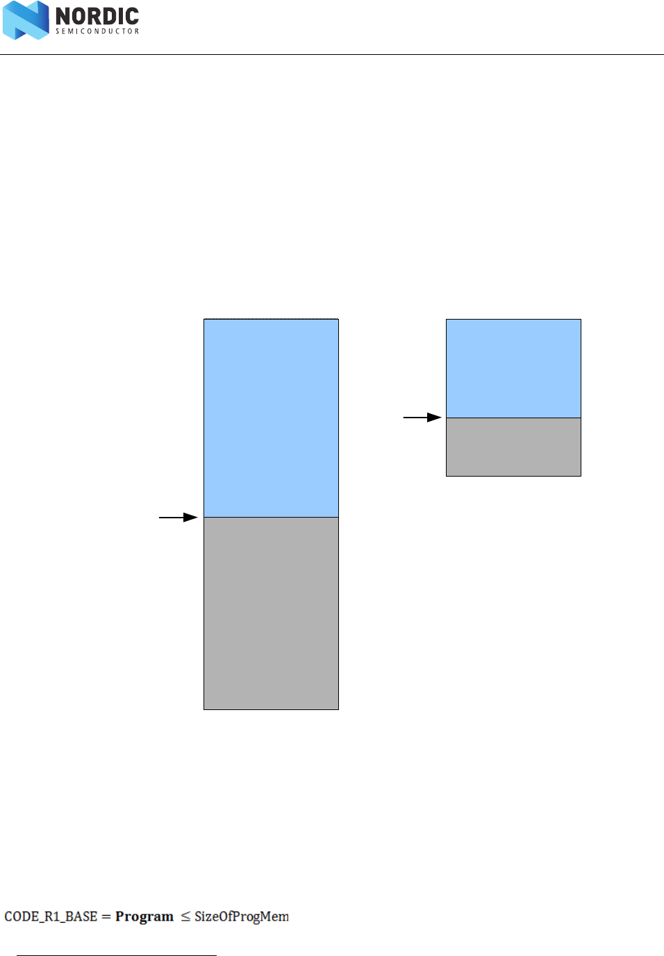
Page 188 of 195
nRF51 Series Reference Manual v2.0 - Low Power Comparator (LPCOMP)
Memory isolation and run-time protection
SoftDevice program and data memory are sandboxed3 to prevent SoftDevice program corruption by the
application ensuring robust and predictable performance.
Program memory and RAM are divided into two regions using registers. Region 0 is occupied by the
SoftDevice while Region 1 is available to the application.
Code regions are defined when programming a SoftDevice by setting a register defining program code
length. RAM regions are defined at run-time when the SoftDevice is enabled. See Figure 74 for an overview
of regions.
Figure 74 Memory region designation
The SoftDevice uses a fixed amount of flash (program) memory and a variable amount of RAM depending
on its state. The flash and RAM usage is specified by size (kilobytes or bytes) and the CODE_R1_BASE and
RAM_R1_BASE addresses which are the usable base addresses of Application code and RAM respectively.
Application code must have base address CODE_R1_BASE while the Application RAM must be allocated
between RAM_R1_BASE and the top of RAM, excluding the allocation for the call stack and heap.
Example Application program code address range:
3. A sandbox is a set of access rules for memory imposed on the user.
Region0
(SoftDevice)
Region1
(Application)
CODE_R1_BASE
0x00000000
0x00000000+
SizeOfProgMem
Program Memory RAM
Region0
(SoftDevice)
Region1
(Application)
RAM_R1_BASE
0x20000000
0x20000000+
SizeOfRAM

Page 189 of 195
nRF51 Series Reference Manual v2.0 - Low Power Comparator (LPCOMP)
Example Application RAM address range assuming call stack and heap location as shown in:
Sandboxing protects region 0 memory. Region 0 program memory cannot be read, written, or erased4 at
runtime. Region 0 RAM cannot be written to by an application at runtime. Violation of these rules, for
example an attempt to write to the protected Region 0 memory, will result in a system Hard Fault as defined
in the ARM® architecture. There are debugger restrictions applied to these regions which are outlined in
Chapter 8 “Memory Protection Unit (MPU)” on page 26 that do not affect execution.
When the SoftDevice is disabled the whole of RAM is available to the application. In the context of an
enabled SoftDevice however, lower address space of RAM will be "consumed" by the SoftDevice and be
marked as write protected.
It is important to note that when the SoftDevice is disabled, the RAM previously used by the application will
not be restored. In practice, the application will in many cases want to specify its RAM region from the
protected memory length until the end of RAM. This is to make application development easy without
having to think about what data to put where.
Note:
• The call stack is conventionally located by the initial value of Main Stack Pointer (MSP) at the
top address of RAM.
• By default RAM1 block is OFF in System ON-mode. If the MSP initial value defined in the
application vector table is in the RAM1 block, the RAM block will be enabled before the
application reset vector is executed.
• Do not change the value of MSP dynamically (i.e. never set the MSP register directly).
• RAM located in the SoftDevice's region will be scrambled once the SoftDevice is enabled.
• The RAM scrambled by the SoftDevice will not be recovered on SoftDevice disable.
Call stack
The call stack is defined by the application. The main stack pointer (MSP) gets initialized on reset to the
address specified by the application vector table entry 0. The application may, in its reset vector, configure
the CPU to use the process stack pointer (PSP) in thread mode. This configuration is optional but may be
used by an operating system (OS), for example, to isolate application threads and OS context memory. The
application programmer must be aware that the SoftDevice will use the MSP as it is always executed in
exception mode.
In configurations without an OS, the main stack grows down and is shared with the nRF51 SoftDevice. The
Cortex-M0 has no hardware for detecting stack overflow, and the application is responsible for leaving
enough space both for the application itself and the nRF51 SoftDevice stack requirements.
It is customary, but not required, to let the stack run downwards from the upper limit of RAM Region 1.
4. An exception is via the Erase All feature which removes all program code from a device.
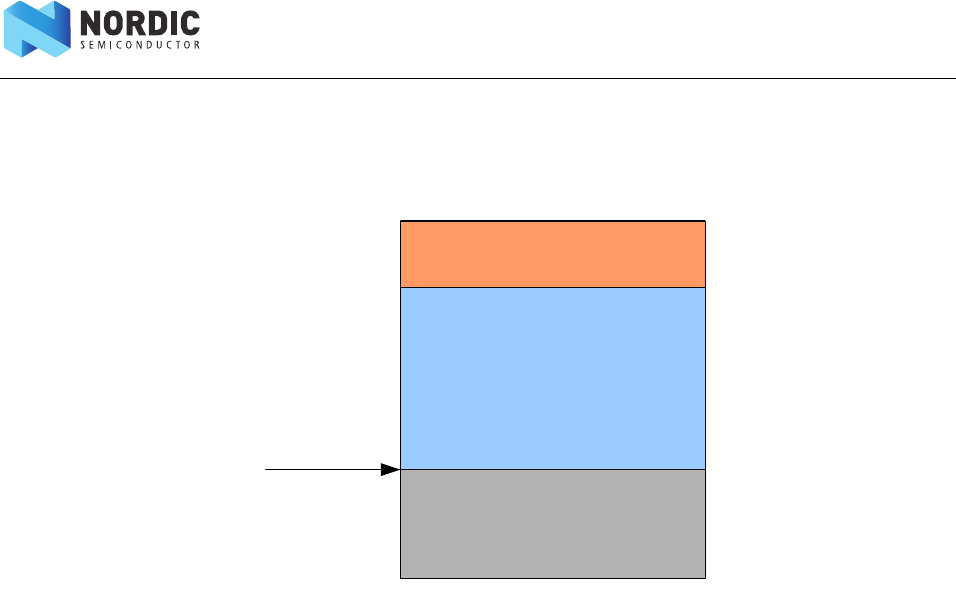
Page 190 of 195
nRF51 Series Reference Manual v2.0 - Low Power Comparator (LPCOMP)
Figure 75 Call stack location example
With each release of a nRF51 SoftDevice its maximum (worst case) call stack requirement is specified, see the
SoftDevice specification for more information. The SoftDevice uses the call stack when LowerStack or
UpperStack events occur. These events are asynchronous to the application so the application programmer
must reserve call stack for the application in addition to the call stack requirement for the SoftDevice.
Heap
At this time there is no heap required by nRF51 SoftDevices. The application is free to allocate and use a
heap without disrupting the function of a SoftDevice.
Peripheral run-time protection
To prevent the application from accidentally disrupting the protocol stack in any way, the application
sandbox also protects SoftDevice peripherals. As with program and data memory protection, an attempt to
perform a write to a protected peripheral will result in a Hard Fault. Protected peripheral registers are
readable by the application, but a write will cause a Hard Fault. Note that peripherals are only protected
while the SoftDevice is enabled, otherwise they are available to the application. See the SoftDevice
specification for an overview of the peripherals that are restricted by the SoftDevice.
Exception (interrupt) management with a SoftDevice
To implement Service Call (SVC) APIs and ensure that embedded protocol real-time requirements are met
independent of application processing, the SoftDevice implements an exception model for execution as
shown in Figure 76 on page 191. Care must be taken when selecting the correct interrupt priority for
application events according to the guidelines that follow. The NVIC API to the SoC Library supports safe
configuration of interrupt priority from the application.
The Cortex-M0 processor has four configurable interrupt priorities ranging from 0 to 3 (with 0 being highest
priority). On reset, all interrupts are configured with the highest priority (0).
RAM
SoftDevice
Region0
Application
Region1
RAM_R1_BASE
0x20000000
0x20000000+
SizeOfRAM
*MSPinitialvalue‐
CallStack
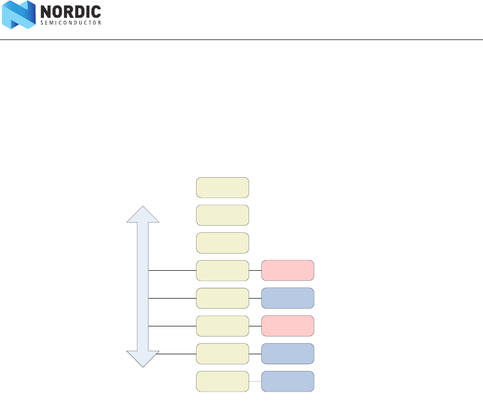
Page 191 of 195
nRF51 Series Reference Manual v2.0 - Low Power Comparator (LPCOMP)
The highest priority (LowerStack) is reserved by the SoftDevice to service real-time protocol timing
requirements and thus must remain unused by the application programmer. The SoftDevice also reserves
priority 2 (UpperStack (SVC) priority). This priority is used by higher level, deferrable, SoftDevice tasks and
the API functions executed as SVC interrupts (see Interface section on page 187).
The application provides two configurable priorities, App(H) and App(L), in addition to the background level
- main.
Figure 76 Exception model
As seen from the figure, App(H) is located between the two priorities reserved by the SoftDevice. This
enables a low-latency application interrupt in order to support fast sensor interfaces. The App(H) will only
experience latency from interrupts in the LowerStack priority, while App(L) can experience latency from
LowerStack, App(H) and UpperStack context interrupts.
Lowest
Priority
Highest
Priority
Reset
Non-maskable
Interrupt
Hard Fault
Cortex M0
Priorities
SoftDevice
priorities
-3
-2
-1
0
1
2
3
Bkgd
P1
P2
P3
MAIN
Application
High - App(H)
UpperStack
(SVC)
Application
Low - App(L)
MAIN
P0 LowerStack
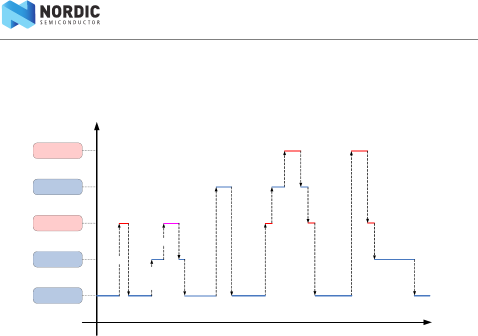
Page 192 of 195
nRF51 Series Reference Manual v2.0 - Low Power Comparator (LPCOMP)
Figure 77 SoftDevice exception examples
Interrupt forwarding to the application
At the lowest level, the SoftDevice Manager receives all interrupts regardless of enabled state. When the
SoftDevice is enabled, some interrupt numbers are reserved for use by the protocol stack implemented in
the SoftDevice and any handler defined by the application will not receive these interrupts. The reserved
interrupts directly correspond to the hardware resource usage of the SoftDevice which can be found in the
corresponding SoftDevice Specification. For example, if a SoftDevice (or embedded protocol stack) requires
the exclusive use of a peripheral “TIMER0”, that peripheral’s interrupt handler can be implemented in the
application, but will not be executed while the SoftDevice is enabled.
All interrupts corresponding to hardware peripherals not used by the SoftDevice are forwarded directly to
the application defined interrupt handler. For the SoftDevice Manager to locate the application interrupt
vectors, the application must define its interrupt vector table at the bottom of code Region 1 (see Figure 78
on page 193). In a majority of toolchains, the base address of the application code is positioned after the top
address of the SoftDevice. Then, the code can be developed as a standard ARM® CortexTM-M0 application
project with the compiler tool creating the interrupt vector table as normal.
LowerStack
Application High
App(H)
UpperStack
(SVC)
Application Low
App(L)
MAIN
Softdevice - Exception
Examples
Priorities
Protocol
Interrupt
Protocol
Interrupt
API Call
Low priority
application
interrupt
API Call
High priority
application
interrupt
API Call
High priority
application
interrupt
Internal
Protocol
Signal
Application
Event
Signal
Protocol
Event
API Calls Sensor
Interrupts
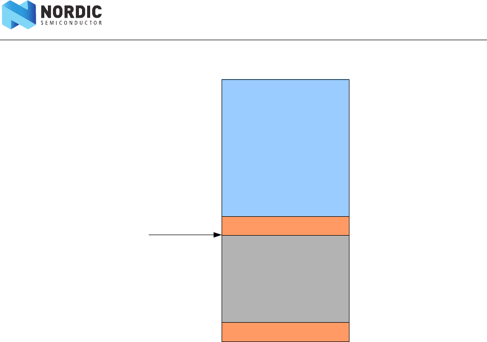
Page 193 of 195
nRF51 Series Reference Manual v2.0 - Low Power Comparator (LPCOMP)
Figure 78 System and application interrupt vector tables
SVC interrupt is handled by SoftDevice manager and the SVC number inspected. If equal or greater than
0x10, the interrupt is processed by the SoftDevice. Values below 0x10 cause the SVC to be forwarded to the
application. This allows the application to make use of a range of SVC numbers for its own purpose, for
example, for an RTOS.
Note: While the CortexTM-M0 allows each interrupt to be assigned to an IRQ level 0 to 3, the priorities
of the interrupts reserved by the SoftDevice cannot be changed. This includes the SVC
interrupt. Handlers running at Application High level have neither access to SoftDevice
functions nor to application specific SVCs or RTOS functions running at Application Low level.
If the SoftDevice is not enabled, all interrupts are immediately forwarded to the application specified
handler. The exception to this is that SVC interrupts with an SVC number above or equal to 0x10 are not
forwarded.
Events - SoftDevice to application
Software triggered interrupts in reserved IRQ slots are used to signal events from SoftDevice to application.
For details on this technique and how to implement handling of these events, refer to the Software
Development Kit (SDK) for your device.
Softdevice
Region0
0x00000000
Application
Region1
ApplicationVectorTable
SystemVectorTable
CODE_R1_BASE
Program Memory
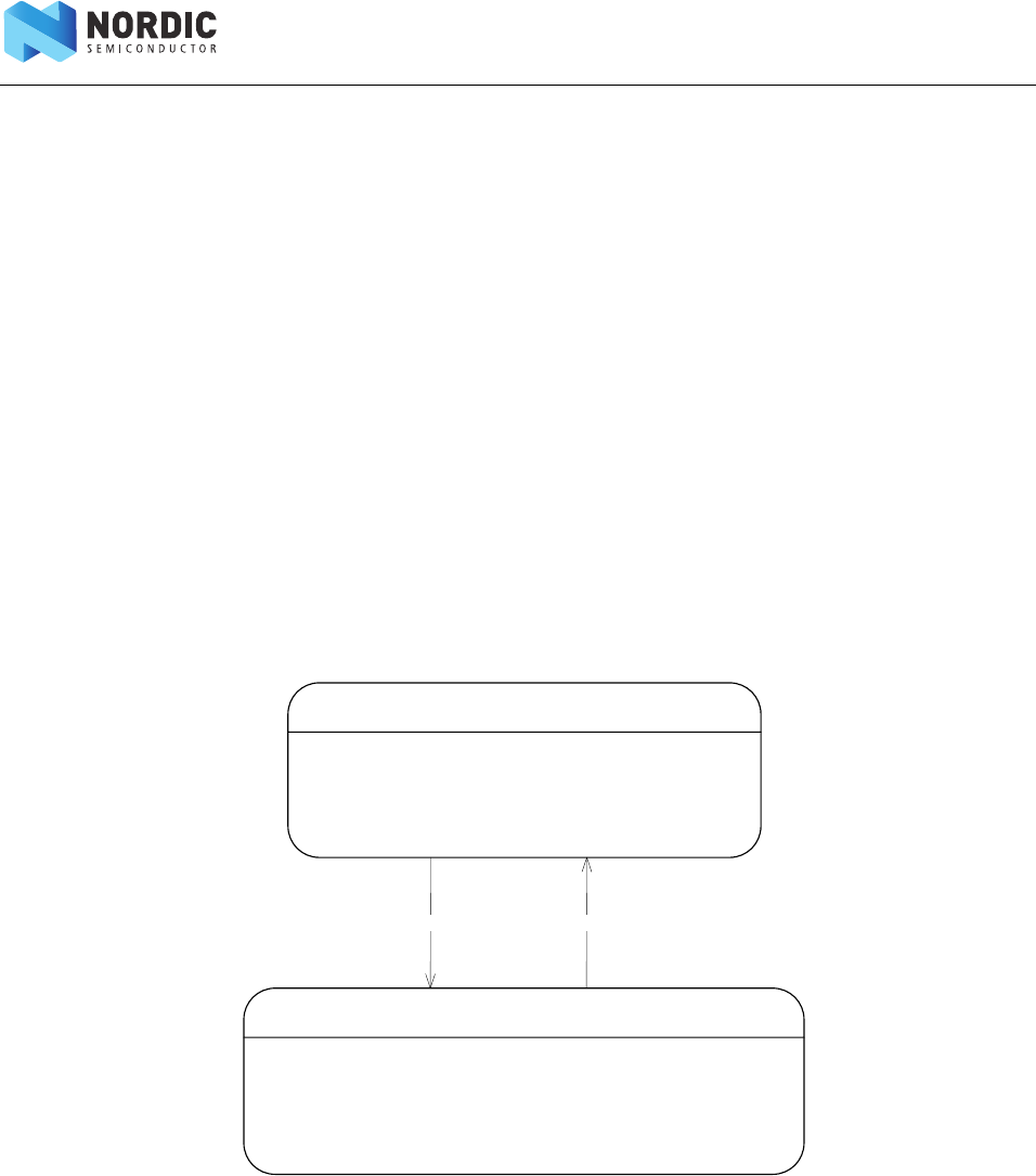
Page 194 of 195
nRF51 Series Reference Manual v2.0 - Low Power Comparator (LPCOMP)
SoftDevice enable and disable
Before enabling the SoftDevice, you cannot use any capabilities of the SoftDevice. This extends to the use of
the SoC library and protocol stack functions. All of the chip’s resources are freely available to the application,
with some exceptions:
• SVC numbers 0x10 to 0xFF are reserved.
• SoftDevice program memory is reserved.
Once the SoftDevice has been enabled, more restrictions apply:
• Some RAM will be reserved.
• Some peripherals will be reserved.
• Some of the peripherals that are reserved will have a SoC library interface.
• Interrupts will not arrive in the application for reserved peripherals.
• The reserved peripherals are reset upon SoftDevice disable.
•nrf_nvic_ functions must be used instead of CMSIS NVIC_ functions for safe use of the
SoftDevice.
• Maximum interrupt latency will be determined by the SoftDevice .
Power management
While the SoftDevice is disabled, the application must implement power management at the highest level.
After a SoftDevice is enabled, the POWER peripheral will be protected. This means that all interactions with
the POWER peripheral must happen through the SoC Library Power API. This API provides an interface for
turning on/off peripherals and checking the power status of peripherals that are not protected by the
SoftDevice. The application will also have the ability to set the other registers in the peripheral and put the
chip in System OFF.
- All Peripherals are available
- All RAM is available
- All Interrupts are forwarded to the application
- SDM API available
Disabled
- Some peripherals are protected by the softdevice,
- Portion of RAM has been protected
- Interrupts for protected peripherals are handled by the softdevice
- SoC library and Protocol-stack APIs are available for the application
Enabled
nrf _enable () nrf _disable()

Page 195 of 195
nRF51 Series Reference Manual v2.0 - Low Power Comparator (LPCOMP)
Error handling
All SoftDevice API functions return an error code on success and failure.
Hard Faults are triggered if an application attempts to access memory contrary to the sandbox rules or
peripheral configurations at runtime.
An assertion mechanism through a registered callback can indicate fatal failures in the SoftDevice to the
application.
