NRF51822_422_DK User Guide N RF51822 Developer Kit V1.2
User Manual: Pdf
Open the PDF directly: View PDF ![]() .
.
Page Count: 56
- 1 Introduction
- 2 Kit content
- 3 Quick start
- 4 Development kit configuration
- 5 Hardware description
- 6 Flash programming and application development
- 7 Debugging the nRF51822
- 8 Testing the physical layer with Direct Test Mode
- 9 Software Development Kit
- 10 Troubleshooting
- Appendix A : Installing drivers and configuring KEIL projects for the SEGGER debugger

Copyright © 2013 Nordic Semiconductor ASA. All rights reserved.
Reproduction in whole or in part is prohibited without the prior written permission of the copyright holder.
nRF51822 Development Kit
nRF51822
User Guide v1.2

Page 2 of 56
nRF51822 Development Kit User Guide v1.2
Contents
1 Introduction............................................................................................................................................... 3
1.1 Minimum requirements................................................................................................................................. 3
1.2 External resources............................................................................................................................................ 3
1.3 Writing conventions........................................................................................................................................ 3
1.4 Development Kit release notes ................................................................................................................... 3
2 Kit content.................................................................................................................................................. 4
2.1 nRF51822 Development Kit hardware content..................................................................................... 4
2.2 Downloadable content .................................................................................................................................. 5
3 Quick start .................................................................................................................................................. 6
3.1 Install the nRF51822 connector module.................................................................................................. 7
3.2 Bluetooth low energy heart rate monitor demo ................................................................................10
4 Development kit configuration ........................................................................................................... 12
4.1 Development environment........................................................................................................................12
4.2 Kit setup .............................................................................................................................................................15
5 Hardware description ............................................................................................................................ 17
5.1 nRFgo nRF51822 DK modules ...................................................................................................................17
5.2 nRF51822 Development Dongle(PCA10000).......................................................................................24
6 Flash programming and application development......................................................................... 27
6.1 Programming and erasing flash using nRFgo Studio .......................................................................27
6.2 Application development ...........................................................................................................................31
7 Debugging the nRF51822..................................................................................................................... 39
7.1 nRF51822 debug features and precautions .........................................................................................40
8 Testing the physical layer with Direct Test Mode ............................................................................ 43
8.1 Kit setup for UART ..........................................................................................................................................43
8.2 Programming the nRF51822 module with DTM.................................................................................45
8.3 DTM testing using nRFgo Studio..............................................................................................................45
9 Software Development Kit ................................................................................................................... 46
9.1 Installing the nRF51 SDK..............................................................................................................................46
10 Troubleshooting ..................................................................................................................................... 47
Appendix A: Installing drivers and configuring KEIL projects for the
SEGGER debugger .................................................................................................................................. 49
Page 3 of 56
nRF51822 Development Kit User Guide v1.2
1 Introduction
The nRF51822 Development Kit (DK) for Bluetooth® low energy/2.4 GHz Proprietary provides a complete
solution for developing, testing, and evaluating the nRF51822 device.
nRF51822 is part of the nRF51 series which offers a range of ultra-low power System on Chip (SoC) solutions
for your 2.4 GHz wireless products.
1.1 Minimum requirements
•nRFgo Starter Kit
• nRFgo Studio v1.14 or later
• Computer with a minimum of 2 USB ports
• Windows XP 32 bit (SP3) or Windows 7
1.2 External resources
• Keil MDK-ARM Lite v4.54 or later https://www.keil.com/demo/eval/arm.htm
• J-Link Software v4.52b or later http://www.segger.com/jlink-software.html
1.3 Writing conventions
This User Guide follows a set of typographic rules that makes the document consistent and easy to read.
The following writing conventions are used:
• Commands are written in Lucida Console.
• Pin names are written in Consolas.
• File names and user interface components are written in bold.
• Internal cross references are italicized and written in semi-bold.
1.4 Development Kit release notes
Date Kit version Description
January 2013 2.0 Fixed known issue in kit v1.0.
New features on PCA10000 v2.0:
• Multicolor LED
• Updated UART configuration.
September2012 1.0 Known issues
PCA10000 v1.0 and PCA10001 v1.0:
• The antenna matching network and layout on these boards is suitable for
applications using TX output power 0 dBm or less. These boards are not
suitable for applications using +4 dBm TX output power.
Page 4 of 56
nRF51822 Development Kit User Guide v1.2
2 Kit content
The nRF51822 DK consists of hardware and access to software components, documentation, and design
files from www.nordicsemi.com.
2.1 nRF51822 Development Kit hardware content
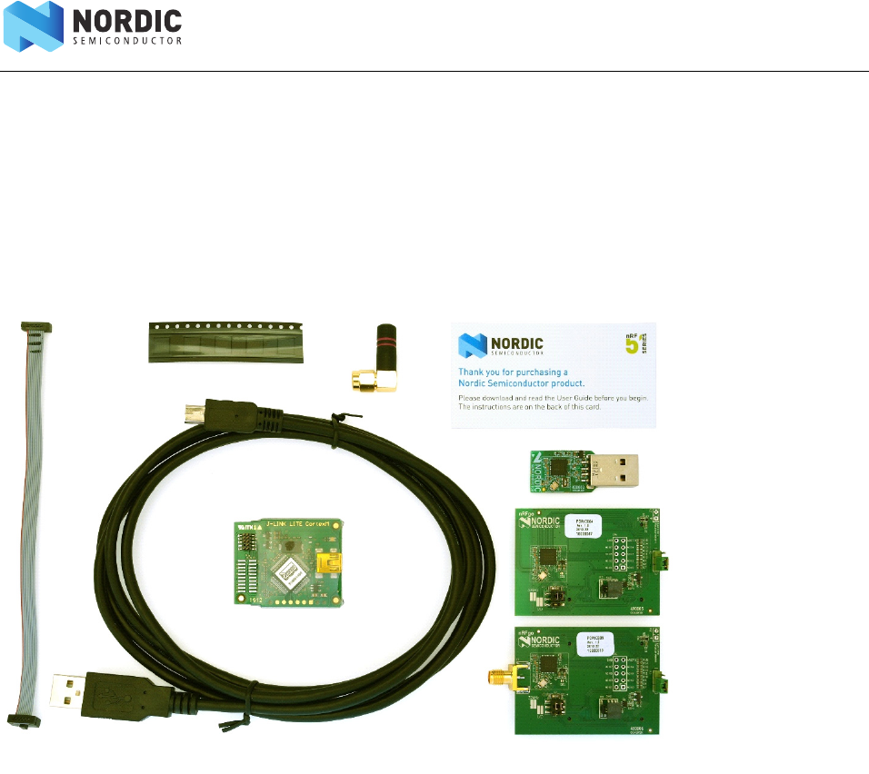
Figure 1 nRF51822 DK hardware content
1 x nRF51822 DK
PCB antenna module
(PCA10004)
1 x nRF51822 DK
SMA connector module
(PCA10005)
1 x nRF51822
Development Dongle
(PCA10000)
1 x J-Link Lite CortexM-9
JTAG/SWD Emulator
1 x Helical monopole SMA antenna
1 x USB cable
5 x nRF51822 chip samples
1 x 10 pin connector

Page 5 of 56
nRF51822 Development Kit User Guide v1.2
2.2 Downloadable content
The nRF51822 Development Kit includes firmware source code, documentation, hardware schematics, and
layout files. To access these files, log in to your My Page account, enter your product key, and download the
files. Instructions can be found in chapter 3 on page 6.
2.2.1 nRF51822 DK software content
•nRFgo Studio
• nRF51 Software Development Kit (SDK)
• Precompiled HEX files
•Source code
•Keil ARM project files
• S110 nRF51822 SoftDevice
2.2.2 nRF51822 DK documentation
• nRF51822 Development Kit User Guide
• nRF51 Series Reference Manual
• nRF51822 PS
• S110 nRF51822 SoftDevice Specification
• nRF51 SDK
• nRF51822 PAN
2.2.3 Schematics, Bill of Materials, PCB layout files, and production files
The ZIP file and its subdirectories contain the hardware design files for the nRF51822 DK.
• Altium Designer files
•Schematics
• PCB layout files
• Production files
• Assembly drawings
• Drill files
•Gerber files
• Pick and Place files
•Bill of Materials
Page 6 of 56
nRF51822 Development Kit User Guide v1.2
3 Quick start
This section shows you how to set up the nRF51822 Development Kit and provides example applications to
help you start programming your device.
Register, download, and install
1. If you have Keil MDK-ARM Lite already installed, go to step 2. Otherwise, download and install Keil
MDK-ARM Lite from https://www.keil.com/demo/eval/arm.htm to your hard drive. Keil downloads
to c:\Keil\ unless you change the location when installing.
2. Download and run the J-Link Software and documentation pack for Windows from
http://www.segger.com/jlink-software.html. The serial number from your SEGGER J-Link hardware
is needed to identify your device and can be found printed on the chip on the J-Link Lite emulator
board.
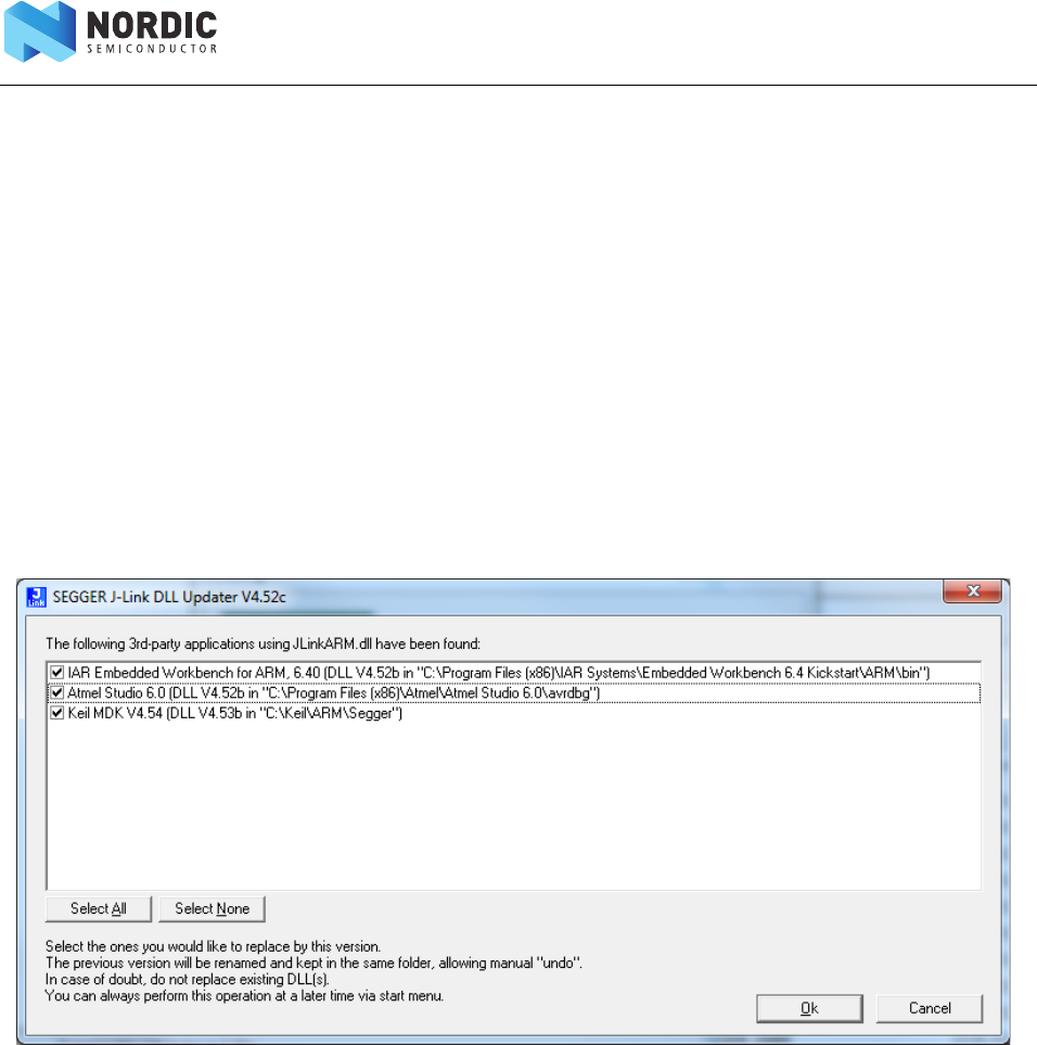
3. During installation you will be prompted to select the IDE that should be updated with the latest
SEGGER DLLs. Check the box for Keil MDK and any other IDEs you want to use with SEGGER.
4. If you are using Keil MDK v4.54, go to:
http://www.segger.com/IDE_Integration_Keil.html#knownproblems. Download JL2CM3 and copy
it to <keil>/ARM/Segger. This patch is necessary for the SEGGER debugger to work.
5. Go to www.nordicsemi.com and log in to your Nordic My Page account.
6. Select My Products from the left menu. This takes you to the My Products page.
7. Enter the product key (included with this kit) into the Product Key field and click Add.
8. From the Add product box, select the product name and click Add.
9. Click the Downloads link in the Overview, My Products table.
10. Download and run the nRF518 SDK installer. Make sure to choose the Keil MDK-ARM installer
option.
Page 7 of 56
nRF51822 Development Kit User Guide v1.2
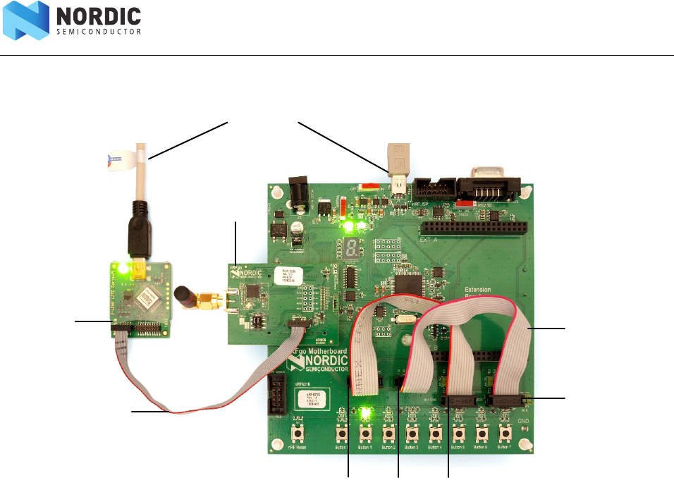
3.1 Install the nRF51822 connector module
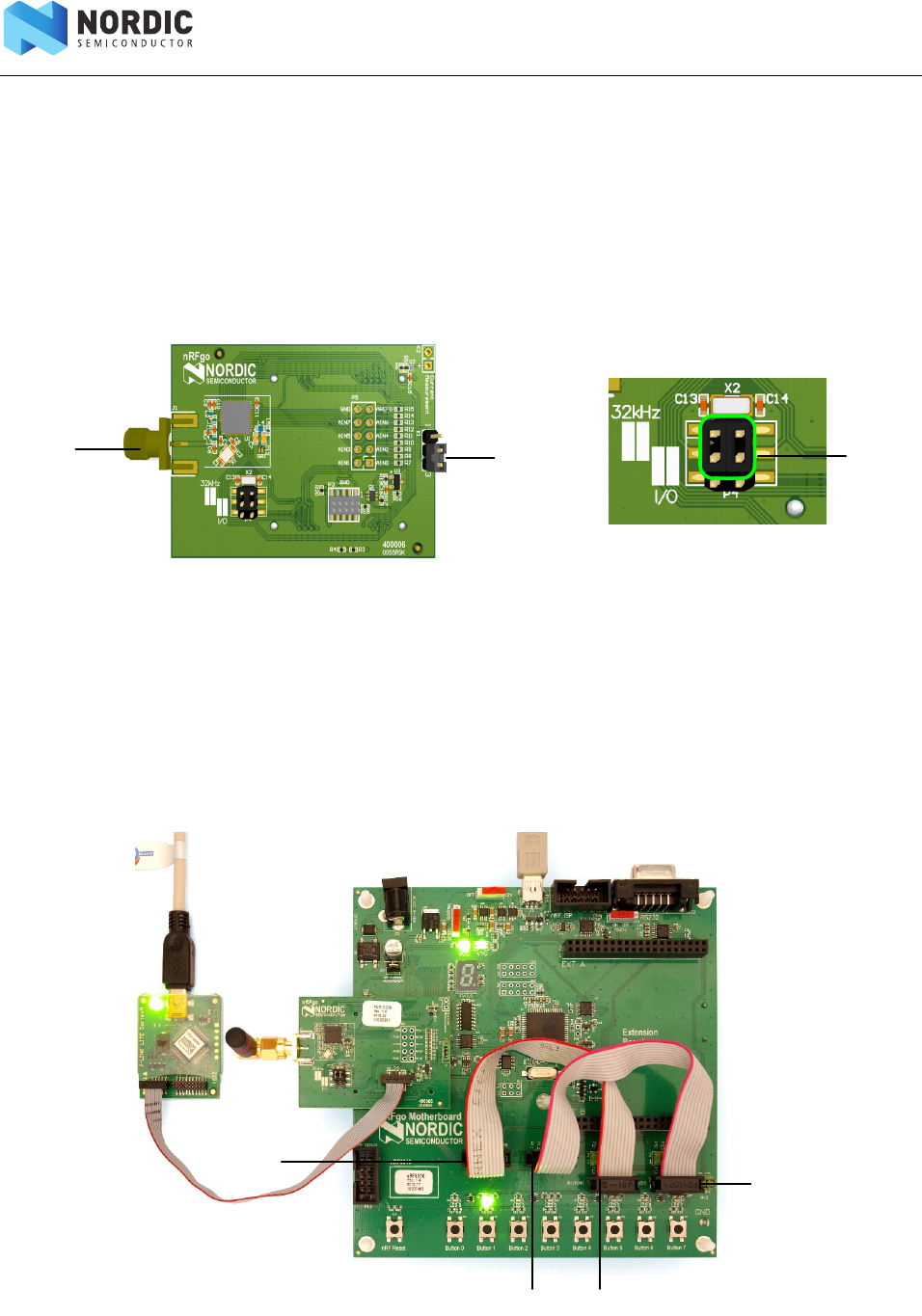
Connect the hardware
1. Screw the antenna into the SMA connector on the nRF51822 DK SMA (PCA10005) connector
module.
2. Ensure that header K1 has a jumper connecting pin 2 and 3. The two upper rows of P4 should
have two jumpers placed vertically matching the 32 kHz marking.
3. Plug the nRF51822 DK SMA connector module into the nRFgo Starter Kit Motherboard (nRF6310).
4. Connect a USB cable from the Motherboard to your computer.
5. Using two 10 pin flat cables (2.54 mm, included in the nRFgo Starter Kit), connect one cable
between P8 (PORT0) and P1 (BUTTONS) and one between P10 (PORT1) and P2 (LEDS) on the
nRFGo Motherboard. Make sure the red marking on the cable is always connected to pin 1, as
shown in the figure below.
6. Connect the SEGGER J-Link board to the nRF51822 module with the 10 pin flat cable (1.27 mm,
provided in the Development Kit).
7. Connect a USB cable from the J-Link board to your computer.
P4
SMA
connector K1 header
P8
P1P10
P2
Page 8 of 56
nRF51822 Development Kit User Guide v1.2
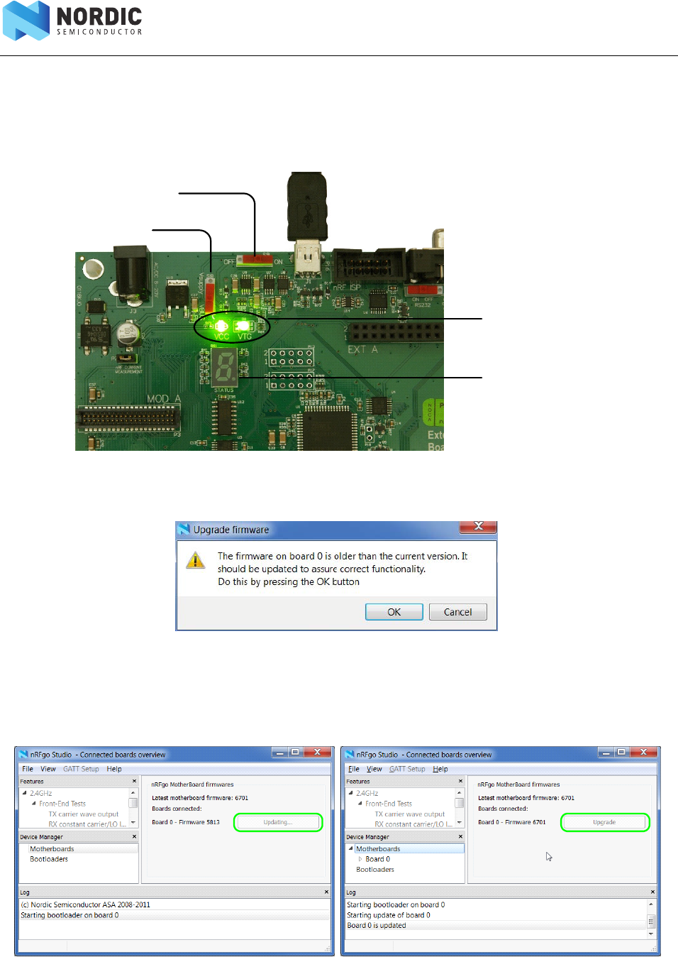
Turn on and set the supply voltage
1. Slide the S8 switch on the Motherboard to VBUS.
2. Slide the On/Off switch on the Motherboard to ON.
3. The VCC and VTG LEDs will light up.
4. Start nRFgo Studio. The Motherboard firmware may require an update, and if needed, you will be
prompted to begin the update. If this occurs, click OK and wait for the update to complete.
Note: While updating the firmware, you will see nRFgo Studio look similar to the image on the left
below. On completion of the update, the “Updating…” message will change to “Upgrade” as
seen in the figure on the right; however, this option is not immediately available after the
latest update and will be greyed out.
S8 switch
On/Off switch
VCC and VTG LED
Board ID
Page 9 of 56
nRF51822 Development Kit User Guide v1.2
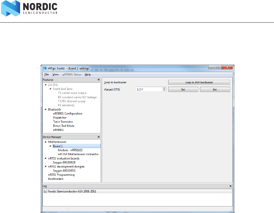
5. Select the desired motherboard from the Device Manager pane in nRFgo Studio. To find the board
ID, look on the 7-segment display on the Motherboard.
6. In nRFgo Studio, you can control the supply voltage (VTG) to the connected nRF51822 module.
Make sure the voltage is set to 3.3 V.
Note: • Please refer to nRFgo Studio's help file for further information. While in nRFgo Studio, press
F1 to open the help file.
•The nRF51822 device is capable of operating at voltages higher and lower than
3.3 V. This can be tested when the debugger is not required for programming or debugging
the application. However, for the J-Link Lite Cortex-M (that is included in the kit) to function
correctly, the supply voltage must be set to 3.3 V on the Motherboard. At all voltages other
than 3.3 V, the J-Link Lite CortexM-9 debugger should be disconnected from the nRF51822
module (SEGGER has debuggers that are capable of debugging in the entire voltage range).
The supply voltage operating range of the nRF51822 device is stated in the Product
Specification.
Start the Blinky project
1. Locate the Blinky project found under <keil path>
\ARM\Device\Nordic\nRF51822\Board\nrf6310\blinky_example\arm.
2. Open the Blinky project in Keil Vision by double clicking the blinky.uvproj file.
3. Select nRF51822 from the Select Target list and click Build or press F7 to compile the Blinky
project.
4. Click the Load icon to download and run the Blinky example firmware. LED0 to LED7 on the
nRFgo Starter Kit Motherboard should now blink sequentially.
Page 10 of 56
nRF51822 Development Kit User Guide v1.2
3.2 Bluetooth low energy heart rate monitor demo
This section shows you how to program a heart rate monitor demo on top of a SoftDevice that will send data
on a Bluetooth link from the heart rate monitor to the Master Control Panel.
Download and program the SoftDevice
Type the product key (included with the Development Kit) into the Product Key field in My Page to
download the S110 nRF51822 SoftDevice.
Follow these steps to program your device:
1. Open nRFgo Studio.
2. In the Device Manager select the motherboard your module is connected to.
3. Select the module.
4. If you have more than one SEGGER debugger connected, you need to select which one you want
to use.
5. Select the Program SoftDevice tab.
6. Click Browse and navigate to the SoftDevice file you downloaded.
7. Click Program.

Page 11 of 56
nRF51822 Development Kit User Guide v1.2
Compile, program, and run the heart rate monitor demo
Note: The Development Dongle must be unplugged during these steps.
1. Locate the Heart Rate demo project found in the folder <keil path>
\ARM\Device\Nordic\nrf51822\board\nrf6310\ble\ble_app_hrs\arm.
2. Open the Heart Rate demo project in Keil Vision by double clicking the ble_app_hrs.uvproj file.
3. Click the Build icon or press F7 to build the project.
4. Only one SEGGER device should be connected to your computer. Make sure it is also connected to
the nRF51822 development module to ensure the program is downloaded to the correct target.
5. Go to the Flash menu and click Download to load the program (or click the Load icon).
6. The Heart Rate demo example will start executing. LED0 should be lit indicating it is advertising.
7. The application advertises for 3 minutes. If a connection isn’t made within this period, the
application sets nRF51822 in System Off.
8. To start advertising again press Button 0.
Install the nRF51822 Development Dongle (PCA10000)
1. Plug the Development Dongle into a USB port on your computer.
2. An icon will appear in the lower right corner of your monitor showing that the drivers are being
installed. Wait until it is ready.
Scan for available Bluetooth low energy devices
1. Open the Master Control Panel from the Start menu (Start > All Programs > Nordic
Semiconductor > Master Control Panel).
2. Make sure the Development Dongle is detected. The Master Emulator item list should show
COMnn-xxxxxxxxx (nn gives the COM port number; xxxxxxxxx is the SEGGER serial number printed
on the dongle). Restart the application if it doesn’t appear in the item list. Before continuing, make
sure you have selected the correct device by verifying the serial number in the item list with the
serial number printed on the Development Dongle.
3. When you use the Development Dongle for the first time, you must first program it with the
Master Emulator Firmware.
a. In the Master Control Panel menu click File and select Flash Programming.
b. Click Browse. This opens a browser that automatically points to the location of the
mefw_nrf51822_<version>_firmware.hex (<version> will be replaced by a number
giving the version of the actual firmware).
The Master Control Panel Firmware file is located in:
<keil path>\ARM\Device\Nordic\nrf51822\board\pca10000\ble\master_emulator
c. Select the Master Emulator Firmware file and click Open.
d. Click Program to start programming the selected device.
e. When the programming is finished click Exit to go back to the main window.
4. Click Start discovery. The Development Dongle will scan for available Bluetooth low energy
devices within range and list them.
5. Select the device CompleteLocalName ‘Nordic_HRM’ in the Discovered Devices list.
6. Click Select device.
7. Click Service Discovery. In the Service discovery pane you will see the services and
characteristics of the device. On the Motherboard LED0 will turn off and LED1 will light up
indicating that is has gone from advertising to connected.
8. Click Enable services. You should see the Heart Rate Measurement characteristic and Battery
Level being notified every few seconds with a different value (the Heart Rate Measurement/
Battery Level value line will blink green for each notification).

Page 12 of 56
nRF51822 Development Kit User Guide v1.2
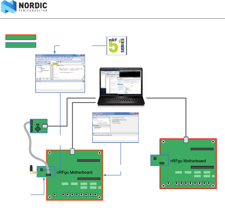
4 Development kit configuration
This chapter shows where to download third party content and how the development environment is set
up.
4.1 Development environment
ARM compiler/IDE (not included in this kit)
All the source code projects and examples can be compiled and used with the Keil Microcontroller
Development Kit (MDK). For full use of the Development Kit source code projects, and to upgrade firmware,
download and install the free KEIL MDK-ARM Lite from https://www.keil.com/demo/eval/arm.htm.
J-Link Lite CortexM-9 driver (not included in this kit)
For installing drivers for the SEGGER J-Link Lite CortexM-9, visit www.segger.com and go to the Downloads
section. Select the J-Link Lite and download the software and documentation. You must correctly install the
drivers for the device to use the J-Link debugger with Keil MDK. See Appendix A “: Installing drivers and
configuring KEIL projects for the SEGGER debugger” on page 49.
4.1.1 Development environment setup
The nRF51822 device can be programmed from several environments. This section shows the development
setup using Keil MDK-ARM. The nRF51822 DK can be configured to develop proprietary 2.4 GHz protocol-
based applications and Bluetooth 4.0 single-mode applications.
For development of proprietary 2.4 GHz protocol-based applications, you need:
•2 x Motherboards (from the nRFgo Starter Kit - not included)
•2 x nRF51822 modules
Page 13 of 56
nRF51822 Development Kit User Guide v1.2
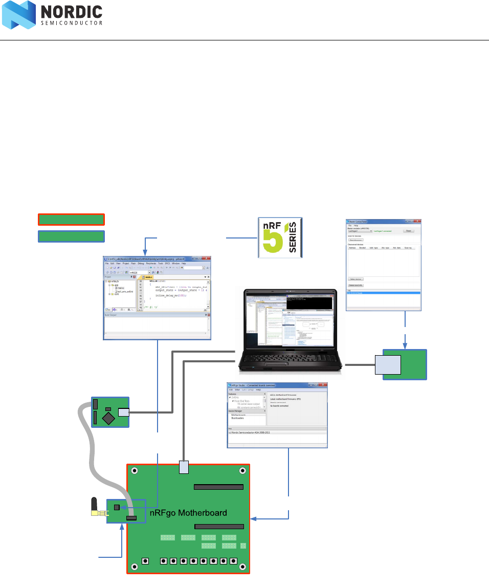
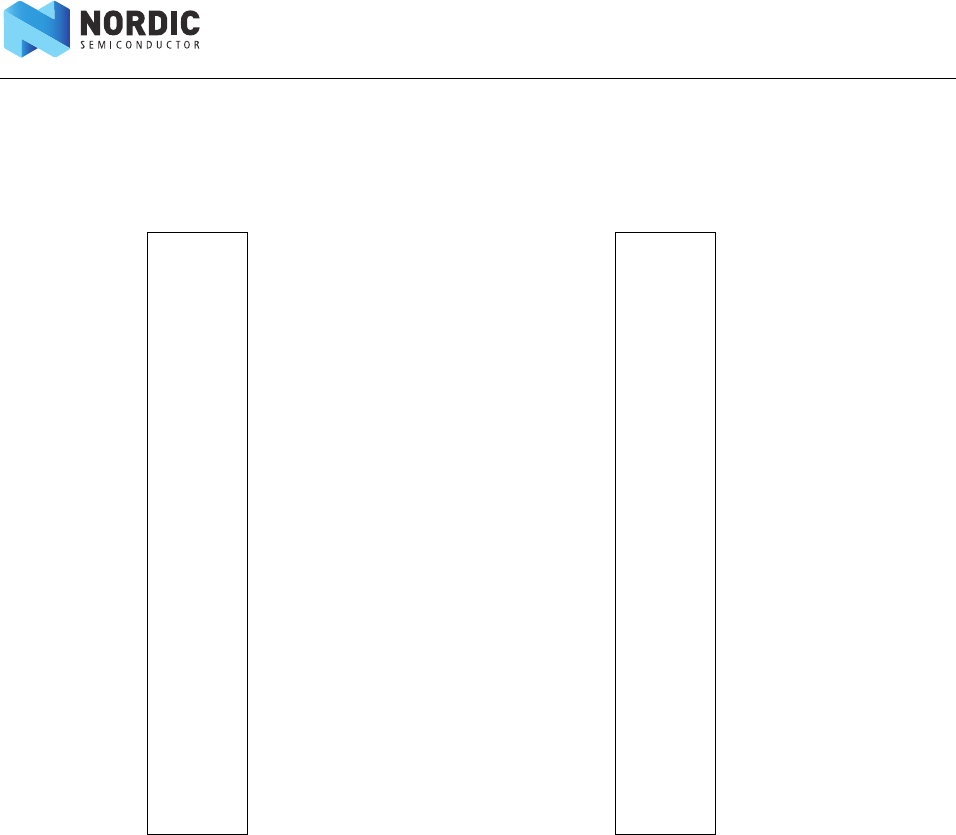
Figure 2 nRF51822 DK configuration for 2.4 GHz based development
USB
USB
USB
Keil µVision IDE
J-Link Lite
Application
Programming &
Erase (Via J-Link)
Examples and Applications
written for Keil
Configure
Voltage
nRFgo Studio
nRFgo Starter Kit
10 pin Flat
Cable
SAMSUNG
nRF51822
module
nRF51822 DK
nRF51 SDK
Page 14 of 56
nRF51822 Development Kit User Guide v1.2
For development or demonstration of Bluetooth 4.0 single-mode applications, you need:
•1 x Motherboard with attached nRF51822 module
•1 x nRF51822 Development Dongle (PCA10000)
• Master Control Panel software
Figure 2 on page 13and Figure 3 below show the relationship between the hardware and software
components, and the Motherboard(s).
Note: The Keil µVision IDE is not included in the kit content.
Figure 3 nRF51822 DK configuration for Bluetooth 4.0 single-mode
USB
USB
Keil µVision IDE
J-Link Lite
Application
Programming &
Erase (Via J-Link)
Examples and Applications
written for Keil
Configure
Voltage
nRFgo Studio
nRFgo Starter Kit
10 pin Flat
Cable
USB
nRF51822
module
SAMSUNG
Control
nRF51822 DK
Master Control Panel
nRF51 SDK
PCA10000
Page 15 of 56
nRF51822 Development Kit User Guide v1.2
4.2 Kit setup
Figure 4 Kit setup
4.2.1 nRFgo nRF51822 DK modules
The nRF51822 modules contain the nRF51822 device and its interfaces (see section 5.1 on page 17 for a
complete description). The modules are plugged into the Motherboard which provides the power supply.
Make sure the jumper on header K1 is placed in the default position as described in section 5.1.8 on page 23.
The Motherboard is connected to your computer with a USB cable and turned on as described in "Turn on
and set the supply voltage" on page 8.
On the Motherboard, the two 10 pin flat cables connecting P8 (PORT0) and P1 (BUTTONS), and P10 (PORT1)
and P2 (LEDS) are required to connect the correct I/Os to the LEDs for the example projects in chapter 2 on
page 4 and for projects in the SDK.
Note: With the nRFgo Studio application you can control the supply voltage (VTG) to the connected
nRF51822 DK module as described in "Turn on and set the supply voltage" on page 8.
P8 P1P10
P2
nRF51 module
USB connected to computer
J-Link Lite
CortexM 10 pin 2.54 mm
flat cable
10 pin 1.27 mm
flat cable
Page 16 of 56
nRF51822 Development Kit User Guide v1.2
4.2.2 nRF51822 Development Dongle (PCA10000)
The nRF51822 Development Dongle (PCA10000) enables you to see the data sent between the dongle and
a single nRF51822 device. The nRF51822 Development Dongle is plugged into a USB port on your computer
as described in "Compile, program, and run the heart rate monitor demo" on page 11.
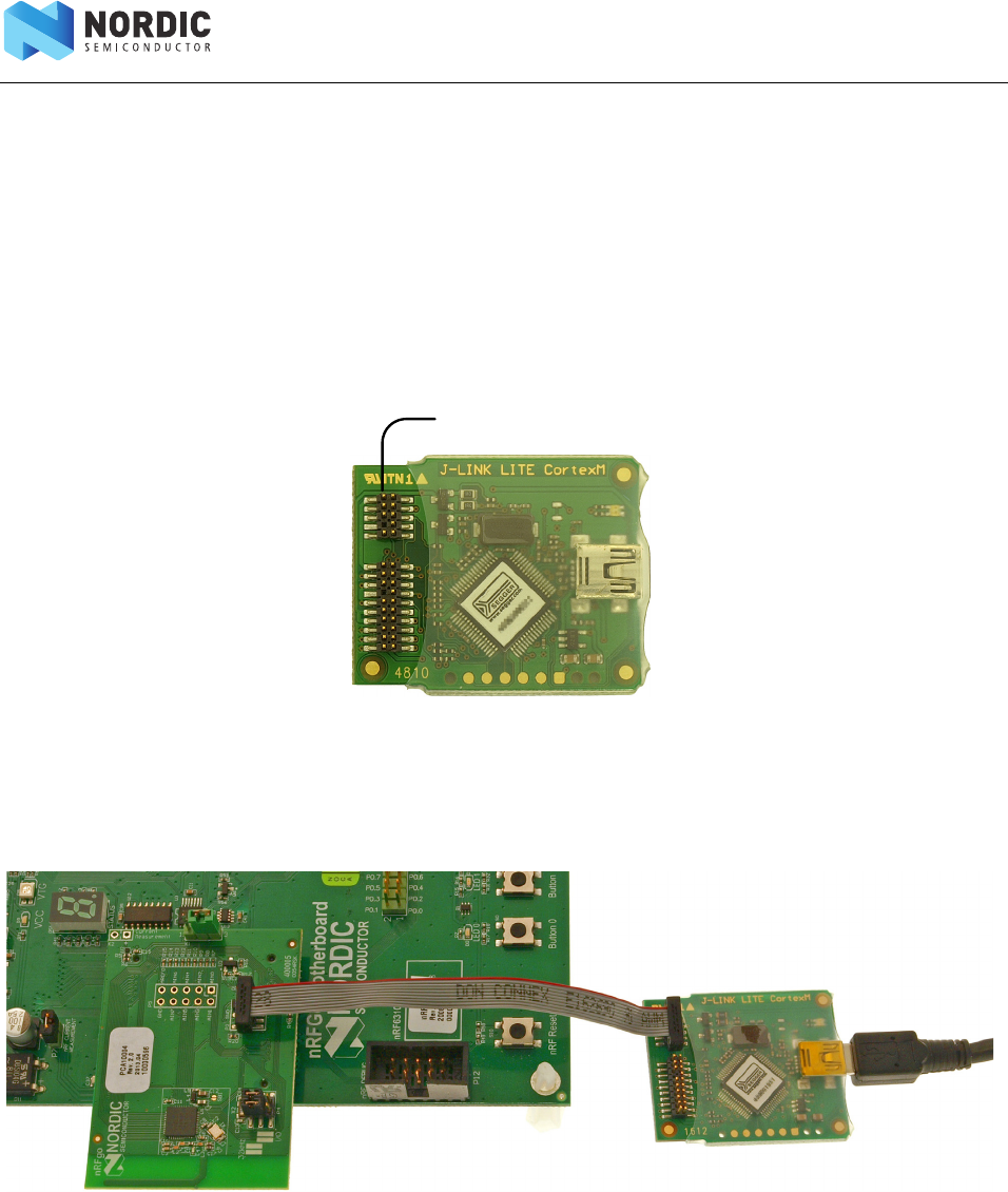
4.2.3 J-Link Lite CortexM-9 JTAG/SWD Emulator
The programming and debugging (SWD) interface of the nRF51822 device is accessed through a 10 pin
connector (P3) on the nRF51822 DK module.
Figure 5 Pin 1 position on the SEGGER J-Link Lite CortexM-9
Connect the JTAG/SWD emulator using the 10 pin 1.27 mm flat cable supplied with the kit to the nRF51822
DK module at P3 and to your computer with a USB cable, as shown in Figure 6.
Figure 6 nRF51822 DK module connected to the SEGGER J-Link Lite CortexM-9
Pin 1
Page 17 of 56
nRF51822 Development Kit User Guide v1.2
5 Hardware description
This chapter describes the nRF51822 DK modules and the nRF51822 Development Dongle (PCA10000).
5.1 nRFgo nRF51822 DK modules
The nRF51822 modules (PCA10004, PCA10005) are delivered with an unprogrammed nRF51822 chip.
5.1.1 Key features
The nRF51822 DK modules have the following key features:
• nRF51822 flash based SoC solution
• 2.4 GHz compatible with nRF24L devices
•Bluetooth low energy compatible
• Current Shunt Monitor (CSM) for current measurements
• nRFgo Motherboard integration
• PCB antenna (PCA10004 only)
• SMA connector compatibility (PCA10005 only)
• SWD interface connector for programming and debugging
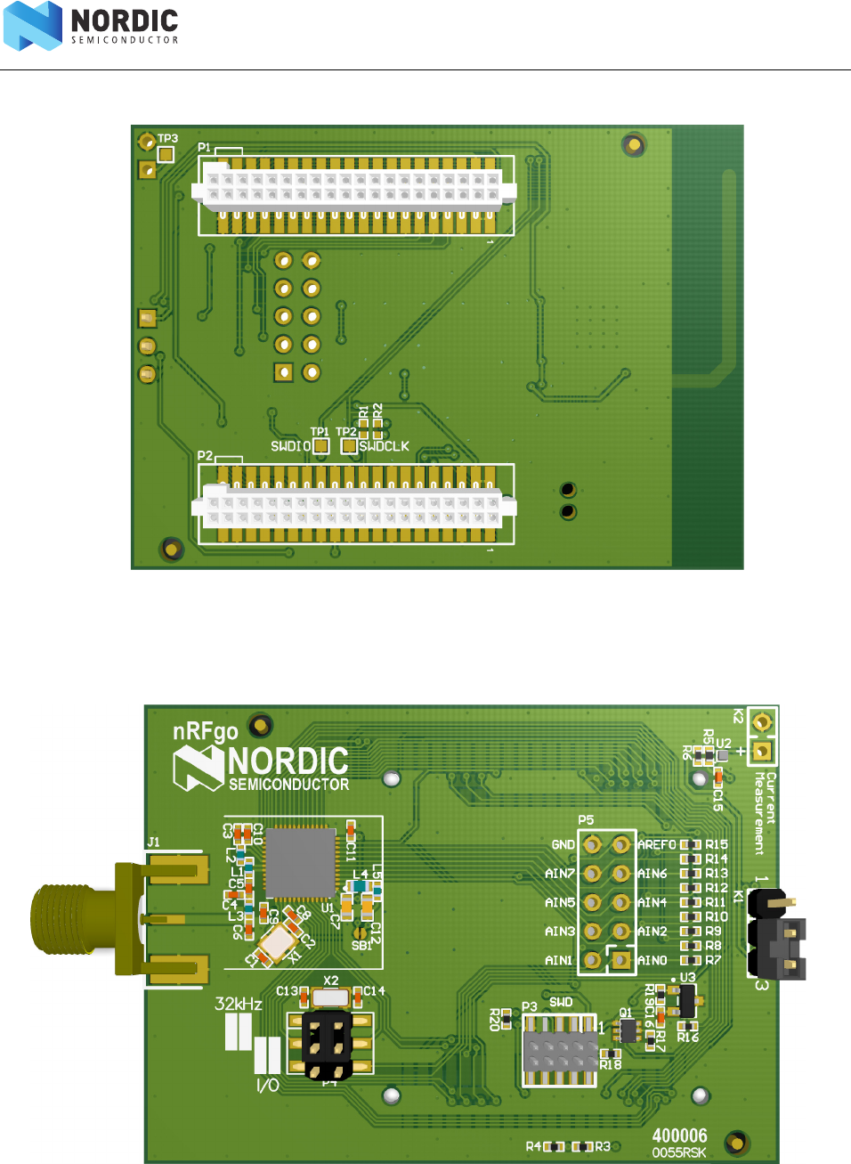
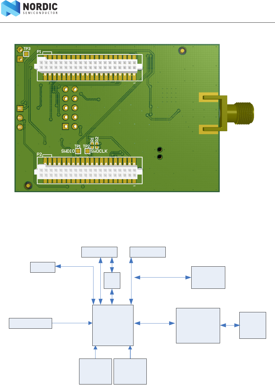
5.1.2 Hardware pictures
Figure 7 nRF51822 DK module (PCA10004) top
Page 18 of 56
nRF51822 Development Kit User Guide v1.2
Figure 8 nRF51822 DK module (PCA10004) bottom
Figure 9 nRF51822 DK module (PCA10005) top
Page 19 of 56
nRF51822 Development Kit User Guide v1.2
Figure 10 nRF51822 DK module (PCA10005) bottom
5.1.3 Block diagram
Figure 11 nRF51822 DK module block diagram
Ext A1 Ext B1
Analog nRF51822 6x6 Matching
network
SMA/
PCB
antenna
CSM
Cortex
Debug
Osc
16 MHz
Osc
32.768 kHz
RESET
Page 20 of 56
nRF51822 Development Kit User Guide v1.2
5.1.4 nRFgo nRF51822 DK module extension
Connectors P1 and P2 on the nRF51822 DK module connect to the Motherboard.
Figure 12 nRF51822 DK module connectors - P1 and P2
VCC 1 2 VCC_nRF' VTG 1 2 VTG
VCC 3 4 VCC_nRF' VTG 3 4 VTG
GND 5 6 GND GND 5 6 GND
P0.00 7 8 P0.01 P0.24 7 8 P0.25
P0.02 9 10 P0.03 P0.26 9 10 P0.27
P0.04 11 12 P0.05 P0.28 11 12 P0.29
P0.06 13 14 P0.07 P0.30 13 14 Not in use
GND 15 16 GND GND 15 16 GND
Not in use 17 18 Not in use Not in use 17 18 Not in use
Not in use 19 20 Not in use Not in use 19 20 Not in use
GND 21 22 GND GND 21 22 GND
Not in use 23 24 Not in use BoardID 23 24 GND
Not in use 25 26 RESET GND 25 26 GND
Not in use 27 28 Not in use Not in use 27 28 BoardID_EE
P0.08 29 30 P0.09 P0.16 29 30 P0.17
P0.10 31 32 P0.11 P0.18 31 32 P0.19
P0.12 33 34 P0.13 P0.20 33 34 P0.21
P0.14 35 36 P0.15 P0.22 35 36 P0.23
GND 37 38 GND GND 37 38 GND
GND 39 40 GND GND 39 40 GND
P1 P2
Page 21 of 56
nRF51822 Development Kit User Guide v1.2
5.1.5 Analog inputs
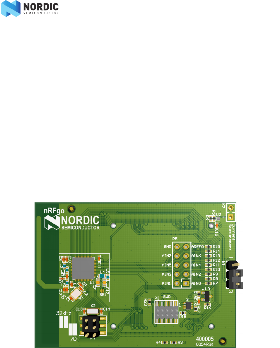
Direct access to the nRF51822 analog input is available on connector P5 on the nRF51822 DK module.
Note: P5 is not mounted on the board.
The analog inputs are routed through the extension connectors to the Motherboard. To avoid noise from
the Motherboard, the 0 resistors must be removed.
Figure 13 Analog inputs connector P5 on the nRF51822 DK board
5.1.6 SWD interface
The programming and debugging interface is accessed through the 10 pin connector P3 on the nRF51822
DK module.
Figure 14 SWD interface connector P3
Table 1 SWD interface connector pin description
AIN0 1 2 AIN1
AIN2 3 4 AIN3
AIN4 5 6 AIN5
AIN6 7 8 AIN7
AREF0 9 10 GND
VTG 1 2 SWDIO
GND 3 4 SWDCLK
GND 5 6 NC
NC 7 8 NC
GND 9 10 NC
Pin Label Description
1 VTG Reference voltage for programmer
2SWDIO Serial Wire Debug Data
3GND Ground
4SWDCLK Serial Wire Debug Clock
5GND Ground
6NC No Connection
7NC No Connection
8NC No Connection
9GND Ground
10 NC No Connection
Page 22 of 56
nRF51822 Development Kit User Guide v1.2
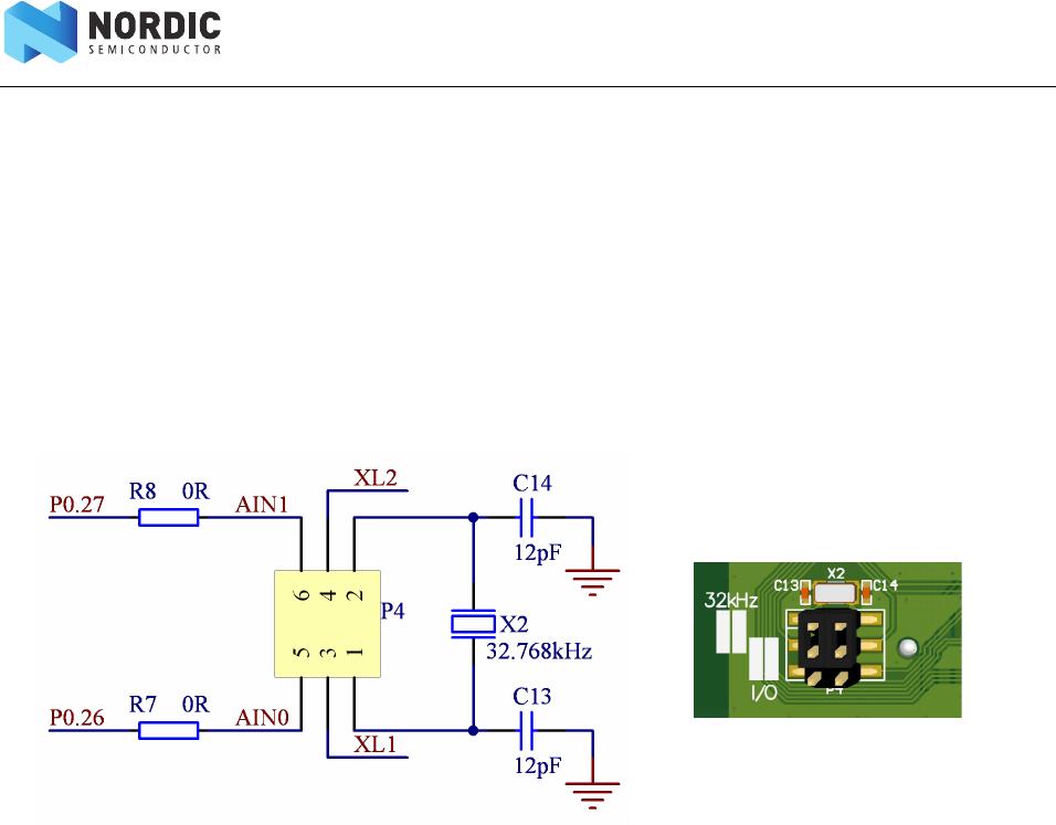
5.1.7 32.768 kHz crystal
The nRF51822 can use an optional 32.768 kHz crystal (X2) for higher accuracy and lower average power
consumption. On the nRF51822 DK module, P0.26 and P0.27 are disconnected from the Motherboard and
connected to the two jumpers on the nRF51822 DK module at the position 32 kHz on connector P4 (Pin 1
and Pin 3 for XL1 and Pin 2 and Pin 4 for XL2). This is the default position of the jumpers when shipped.
Note: The 32.768 kHz crystal has to be selected for the Bluetooth examples to work.
If the jumpers are placed in the position I/O on connector P4 (Pin 3 and Pin 5 for XL1 and Pin 4 and Pin 6 for
XL2), P0.26 and P0.27 connects to the Motherboard and can be used for normal I/O.
Figure 15 32.768 kHz crystal circuit schematic and PCB
Page 23 of 56
nRF51822 Development Kit User Guide v1.2
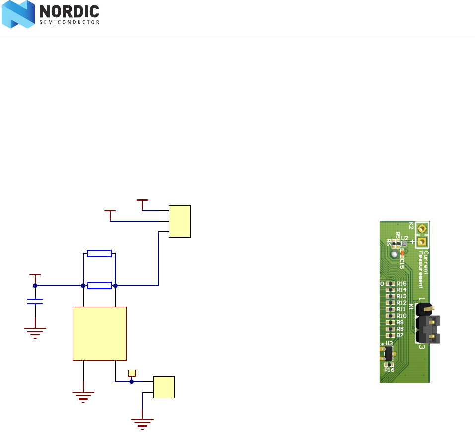
5.1.8 Current measurements
The current drawn from the nRF51822 device can be monitored using the Current Shunt Monitor (CSM),
INA216 (U2). The gain of the CSM is set to 200 V/V for lowest possible drop voltage.
For current measurements using the CSM, the jumper on connector K1 must be placed on Pin 2 and Pin 3.
This is the default position of the jumpers when shipped. Current on the nRF51822 module is measured on
connector K2 as voltage proportional to the current.
For current measurements using the jumper P7 on the Motherboard, the jumper on connector K1 must be
placed on Pin 1 and Pin 2.
Figure 16 Current measurement circuit schematic and PCB
!
"
"
#
"
Page 24 of 56
nRF51822 Development Kit User Guide v1.2
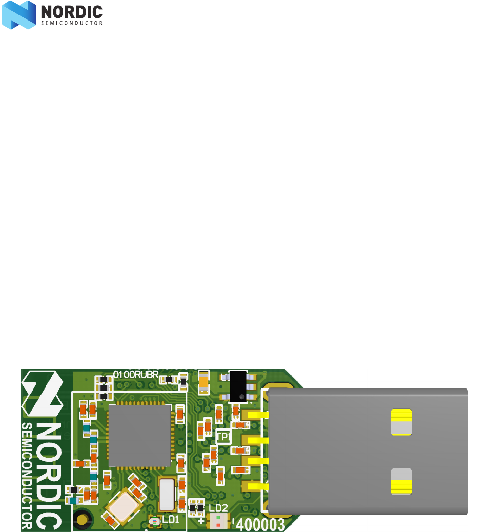
5.2 nRF51822 Development Dongle(PCA10000)
The nRF51822 Development Dongle (PCA10000) can be used as a development platform for the nRF51822
device. It features an on-board programming and debugging solution from SEGGER. In addition to radio
communication, the nRF51822 device can communicate with a computer through a virtual COM port
provided by the SEGGER chip. The PCA10000 can be loaded with Master Emulator firmware, that when
combined with the Master Control Panel, gives you a peer device for nRF51822 that you can use to test the
wireless connection.
Note: PCA10000 can be reprogrammed if overwritten.
5.2.1 Key features
The PCA10000 has the following key features:
• nRF51822 flash based SoC solution
•Bluetooth low energy compatible
• 2.4 GHz compatible with nRF24L devices
• USB to UART bridge
• SEGGER J-Link OB programming and debugging capabilities
5.2.2 Hardware pictures
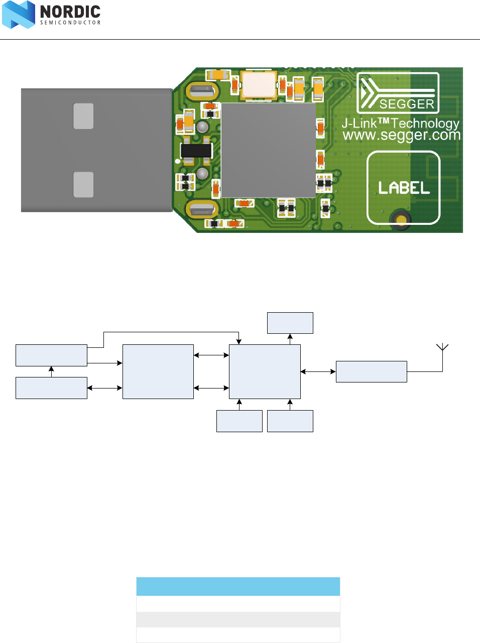
Figure 17 PCA10000 top side
Page 25 of 56
nRF51822 Development Kit User Guide v1.2
Figure 18 PCA10000 bottom side
5.2.3 Block diagram
Figure 19 PCA10000 block diagram
Figure 20
5.2.4 Mulitcolor LED
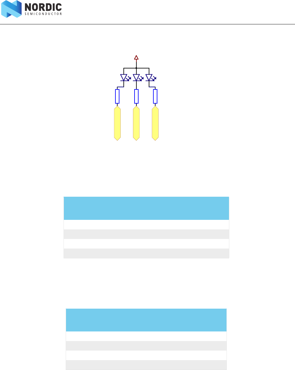
The Development Dongle (PCA10000) is equipped with a multicolor RGB LED. The LED is connected to
dedicated I/Os on the nRF51822 chip. The connections are shown in Table 2.
Table 2 LED connection
Color GPIO
Red P0.21
Green P0.22
Blue P0.23
USB
Voltage regulator
Matching networknRF51822
Antenna
Segger OBVBUS
Data UART
SWD
VCC_nRF
Osc
32.768 kHz
Osc
16 MHz
RGB
LED
Page 26 of 56
nRF51822 Development Kit User Guide v1.2
The LEDs are active low, meaning that writing a logical zero (‘0’) to the output pin will illuminate the LED.
Figure 21 LED configuration
5.2.5 UART configuration
The Development Dongle v1.0 UART lines are connected to pins P0.00 to P0.03 as shown in Table 3.
Table 3 Development Dongle v1.0 UART configuration
The Development Dongle v2.0 UART lines are connected to pins P0.08 to P0.11 as shown in Table 4.
Table 4 nRF51822 Development Dongle UART configuration
Note: The UART signals are routed directly to the SEGGER chip. The pins should only be used for
UART. In order to use the USB to UART bridge, the software on the nRF51822 has to enable
flow control. For details on how to set up the UART with flow control, see the nRF51 Series
Reference Manual.
nRF51822 SEGGER IC
GPIO UART UART
P0.00 RTS CTS
P0.01 TXD RXD
P0.02 CTS RTS
P0.03 RXD TXD
nRF51822 SEGGER IC
GPIO UART UART
P0.08 RTS CTS
P0.09 TXD RXD
P0.10 CTS RTS
P0.11 RXD TXD
Page 27 of 56
nRF51822 Development Kit User Guide v1.2
6 Flash programming and application development
The nRF51822 chip is shipped without pre-programmed software. This gives you the option of developing
your application directly onto the chip or alternatively, by using our S110 nRF51822 SoftDevice, which is a
Bluetooth low energy peripheral protocol stack solution. For more information, see the S110 nRF51822
SoftDevice Specification.
In this chapter we describe how to program and erase the S110 nRF51822 SoftDevice or another application
HEX file on the nRF51822 chip.
If you want to start developing on the nRF51822 chip without using the S110 nRF51822 SoftDevice see
section 6.1.4 on page 29.
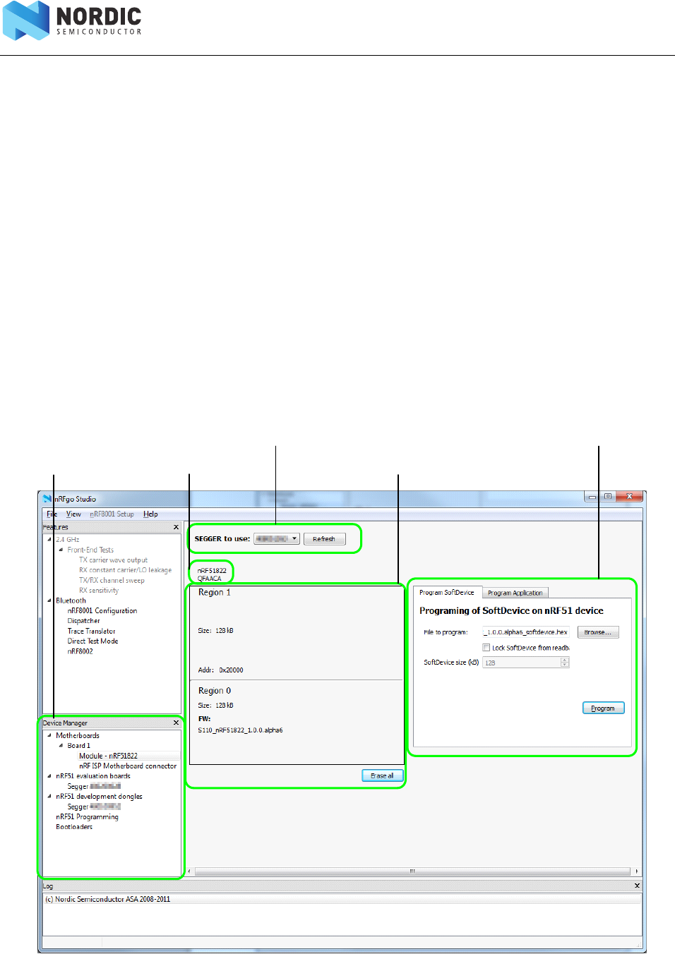
6.1 Programming and erasing flash using nRFgo Studio
Use nRFgo Studio to program or erase a SoftDevice or application HEX file onto the nRF51822 chip.
Note: For details on memory organization and protection see the nRF51 Series Reference Manual.
Figure 22 nRFgo Studio dashboard
List of SEGGER debuggers Code memory
- Memory readback protection
- SoftDevice identification
Programming tools
Device Manager nRF51 chip identification

Page 28 of 56
nRF51822 Development Kit User Guide v1.2
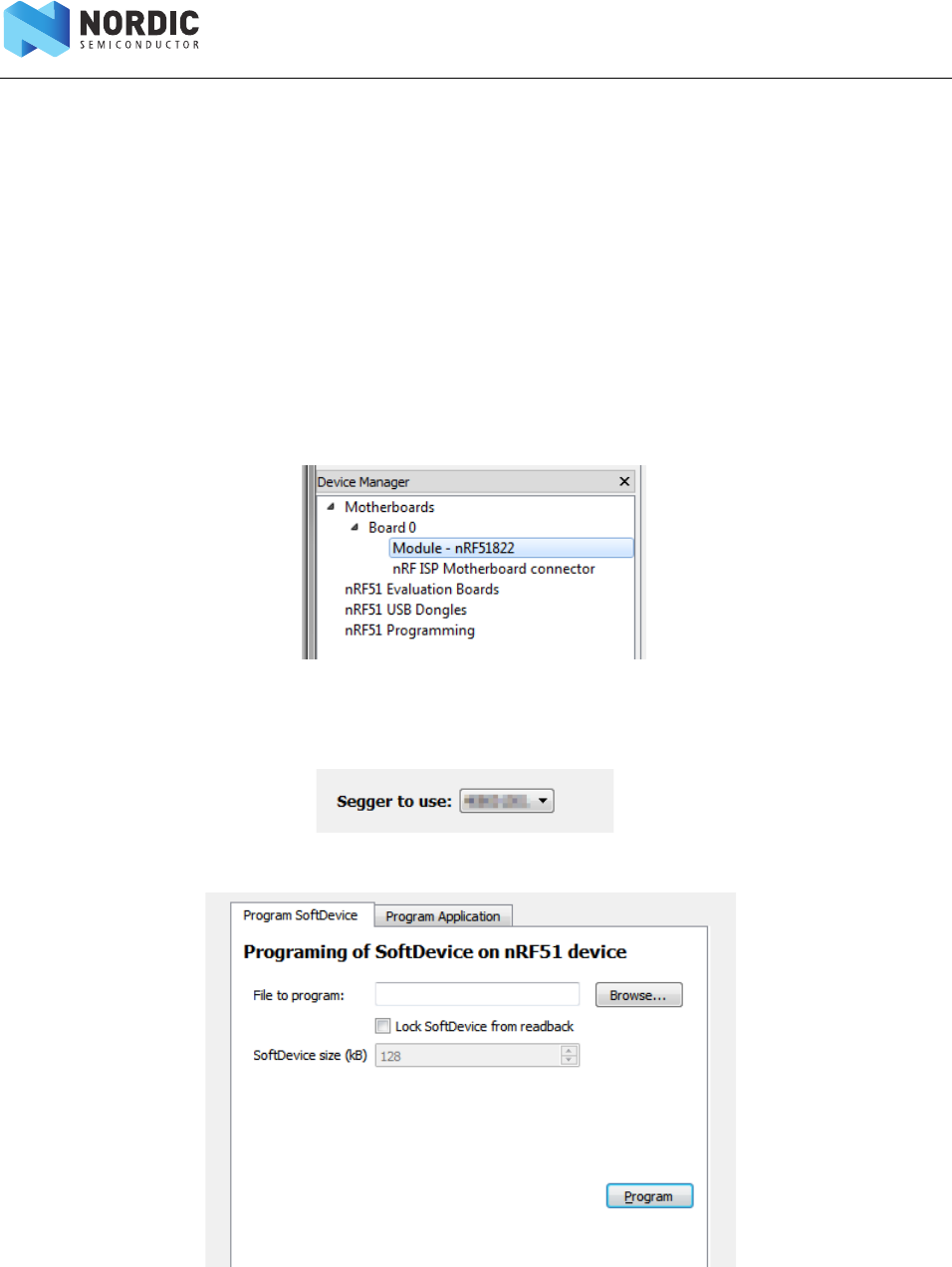
6.1.1 Selecting a board to program
1. Open nRFgo Studio.
2. In the Device Manager pane select which board to program or erase.
3. The nRF51822 DK modules (PCA10004/ PCA10005) cannot be selected directly. The boards must
be selected through the J-Link debugger connected to them. To do this, you either select the
actual module located under Motherboard > Boardx or by clicking on nRF51 Programming.
4. Select the debugger you want to use from the list of available J-Link debuggers under Segger to
use.
6.1.2 Identifying the nRF51 chip and chip content
When you select a board, nRFgo Studio identifies the nRF51822 chip and how its memory is organized.
The following chip and memory information is displayed:
•nRF51 chip identification - Identifies the chip by name and code variant (for example,
nRF51822 QFAACA). If the debugger is not connected to the chip, or the debugger has a
problem communicating with the chip, it will show the following message “No device
detected. Ensure that you have the SEGGER connected correctly to the board and that the
board is powered and configured for debugging.”
•Code memory - Shows how the code memory is organized in one or two regions (Region 0
and 1) and the size of each region. For devices containing a SoftDevice, the code memory is
divided in two regions, with the SoftDevice in Region 0. The tool shows you how much
memory is used by the SoftDevice and how much is left for the application.
• Memory readback protection - Shows how the readback protection is set. The two
possible options are readback protection on Region 0 or readback protection of the
whole code memory. If there is only one region the option is readback protection on
(All) or off.
• SoftDevice identification - nRFgo Studio tries to identify the firmware located in the
chip at Region 0. For the firmware that it recognizes it prints the ID (in clear text) for the
unrecognized firmware it prints the FWID number.
6.1.3 Erase all
Use Erase all in the following situations:
• You have a chip that is programmed with a SoftDevice but you want to remove it and have a
blank chip.
• You have programmed an application on a clean chip using nRFgo Studio with the option
“Lock entire chip from readback”.
To use the Erase all function, follow the steps in section 6.1.1 on page 28. Then click Erase all.
Page 29 of 56
nRF51822 Development Kit User Guide v1.2
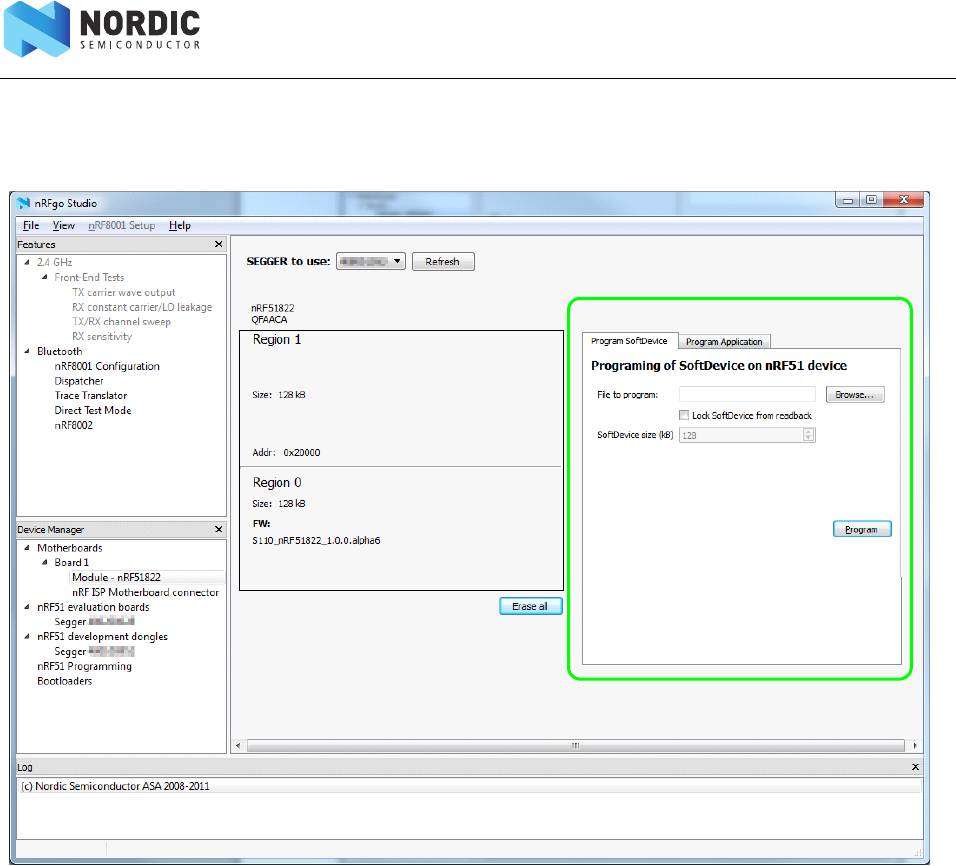
6.1.4 Programming a SoftDevice
This function lets you program the SoftDevice onto the chip.
1. Follow the steps in section 6.1.1 on page 28 and then select the Program SoftDevice tab.
2. Click Browse and select the HEX file to program.
3. Select whether to enable or disable readback protection of Region 0.
4. Set the SoftDevice size. This sets the size of the code memory region 0 and will not be available if
the size is defined by the HEX file.
Note: The S110 nRF51822 SoftDevice can be downloaded from www.nordicsemi.com by logging
into your MyPage account and entering the product key printed in the Development Kit.
Page 30 of 56
nRF51822 Development Kit User Guide v1.2
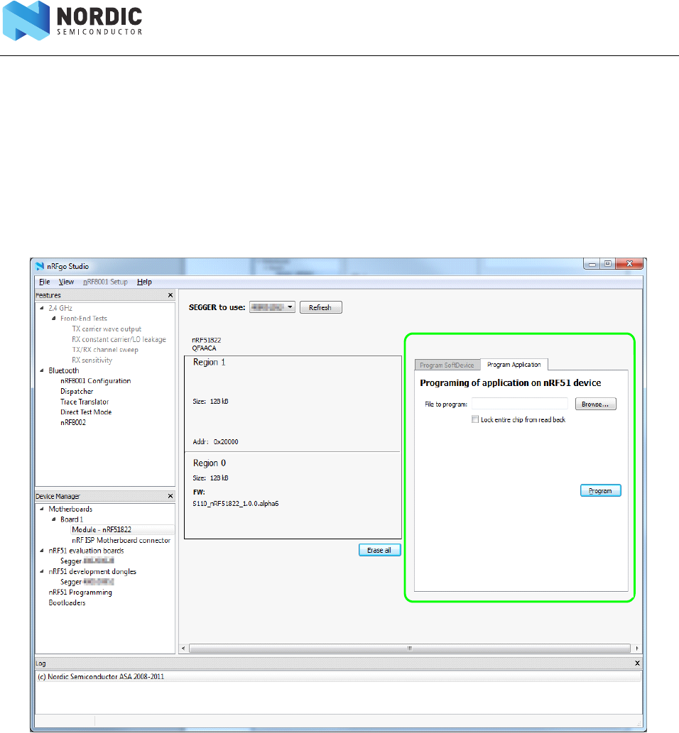
6.1.5 Programming an application
This function lets you program an application onto the chip.
Before nRFgo Studio starts programming it verifies that the HEX file matches the actual memory
configuration. If it matches, nRFgo Studio continues with the programming, if not it stops the programming
and returns an error message. For example, if an application requires the SoftDevice on the chip, it will check
the memory configuration for the SoftDevice before programming the chip.
Note: This programming will not set up any memory Regions.
1. Follow the steps in section 6.1.1 on page 28 and then select the Program Application tab.
2. Click Browse and select the HEX file to program.
3. Select whether to enable or disable readback protection of the entire chip. If you enable readback
protection, you will have to do an Erase All to reprogram the chip again.
Note: A chip that is programmed with Lock entire chip from read back enabled will not work with
a development toolchain. To make it work you must perform Erase all.
Lock entire chip from read back can be used to prevent an accidental overwrite of the chip
content.
Page 31 of 56
nRF51822 Development Kit User Guide v1.2
6.2 Application development
The user application is compiled, linked, and downloaded independently from the SoftDevice. This means
that developing and debugging on a chip pre-programmed with a SoftDevice is similar to that of a blank
chip. The main differences are memory layout and the call stack size.
6.2.1 Configuring memory layout
Specific SoftDevice versions and stacks could have different requirements. Please review these before
proceeding.
The applications vector table must be set up differently depending on whether it will run on a chip that is
blank or pre-programmed with a SoftDevice.
The SoftDevice program area starts at address 0x0 and has a predefined size. The application start vector
must be placed right after the SoftDevice. The available size has to be set so that it uses the remaining
memory for the application. Similarly, the SoftDevice data area starts at the lowest RAM address. The
application data area must be placed after the SoftDevice data area.
Table 5 shows examples for setting up the start address and size depending on the code and data size used
by the SoftDevice. The example is based on a chip with 256 kB of code memory and 16 kB of RAM.
Table 5 SoftDevice memory layout
Note: See the nRF51822 Product Specification for details on the total code memory and RAM
available in the device. The amount of code memory and RAM used by the SoftDevice is
described in the S110 nRF51822 SoftDevice Specification.
There are two ways to configure the memory layout:
•Using Keil IDE
• Using a Scatter file (not covered in this document)
Note: The example code given by Nordic Semiconductor configures the memory layout in the Keil
IDE. Scatter file loading is not available when using the evaluation version of Keil IDE.
Device
configuration
SoftDevice App. code
start address
Available code
memory
App. data
start address
Available
RAM
Code memory
usage RAM usage
Blank chip 0 kB 0 kB 0x0 0x40000 0x20000000 0x4000
SoftDevice A 64 kB 2 kB 0x10000 0x30000 0x20000800 0x3800
SoftDevice B 128 kB 8 kB 0x20000 0x20000 0x20002000 0x2000
Page 32 of 56
nRF51822 Development Kit User Guide v1.2
6.2.1.1 Memory layout configuration in Keil IDE
To access the Keil IDE memory layout:
1. Click the Project menu and select Options for Target.
2. Select the Linker tab.
3. Check Use memory layout from Target Dialog.
Figure 23 Keil linker settings
Page 33 of 56
nRF51822 Development Kit User Guide v1.2
4. Select the Target tab.
5. In Read/Only Memory Areas, define values for Start and Size.
6. In Read/Write Memory Areas, define values for Start and Size as seen in Figure 24.
7. Click OK.
Below is an example configuration for an application using a chip with 256 kB of code memory and 16 kB of
RAM, and a SoftDevice using 128 kB of code memory and 8 kB of RAM (SoftDevice B described in Table 5 on
page 31).
• Base code memory address 0x20000 and available code memory size is 0x20000 (128 kB).
• Base RAM memory address 0x20002000 and available RAM size is 0x2000 (8 kB).
Figure 24 Memory layout with example SoftDevice
Table 6 Memory layout
Memory Description
IROM1 Start Specify the start address for the application code
Size Specify available code size for the application code
IRAM1 Start Specify start address for the application data
Size Specify available RAM size for the application data
Page 34 of 56
nRF51822 Development Kit User Guide v1.2
6.2.2 Shared call stack
The user application shares the call stack with the SoftDevice if the SoftDevice is loaded on the chip. The
application must reserve enough memory for both itself and the SoftDevice in the call stack. The call stack
size required by the SoftDevice varies between devices and protocol stack versions, and is supplied in the
S110 nRF51822 SoftDevice Specification.
The user application sets its call stack size plus the amount needed by the SoftDevice. It then writes the
stack pointer at the first address of the application Reset Vector.
Note: Using Keil with the ARMCC toolchain, the call-stack size can be set using the Stack_Size
definitions in your projects startup file, typically arm_startup_nrf51.s.
Stack_Size EQU 0x400 ; The application call-stack size + protocol
call-stack size
AREA STACK, NOINIT, READWRITE, ALIGN=3
Stack_Mem SPACE Stack_Size
__initial_sp
Page 35 of 56
nRF51822 Development Kit User Guide v1.2
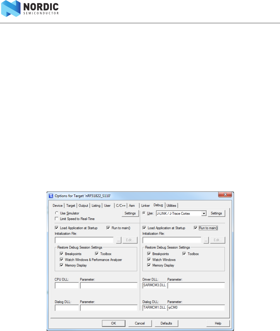
6.2.3 Debugger configuration
Project files delivered in the SDK are configured and ready for download and debugging. If a new
application project is used, the debugger must be properly configured. To configure the debugger:
1. In Keil, select Options for Target (ALT+F7) from the Project menu. The Options for Target dialog
box appears.
2. Select the Debug tab.
3. Apply the Use option and select the J-Link/J-Trace debugger from the list.
4. Set Driver DLL to SARMCM3.DLL.
5. Set Dialog DLL to TARMCM1.DLL.
Other options can be selected as needed. To take full advantage of the debugger and its features, the
following are advised:
•Breakpoints
• Load Application at Startup
• Memory Display
• Toolbox
•Watch Windows
Figure 25 Debugger options
6. Click Settings next to the Use field in the top right of the window.
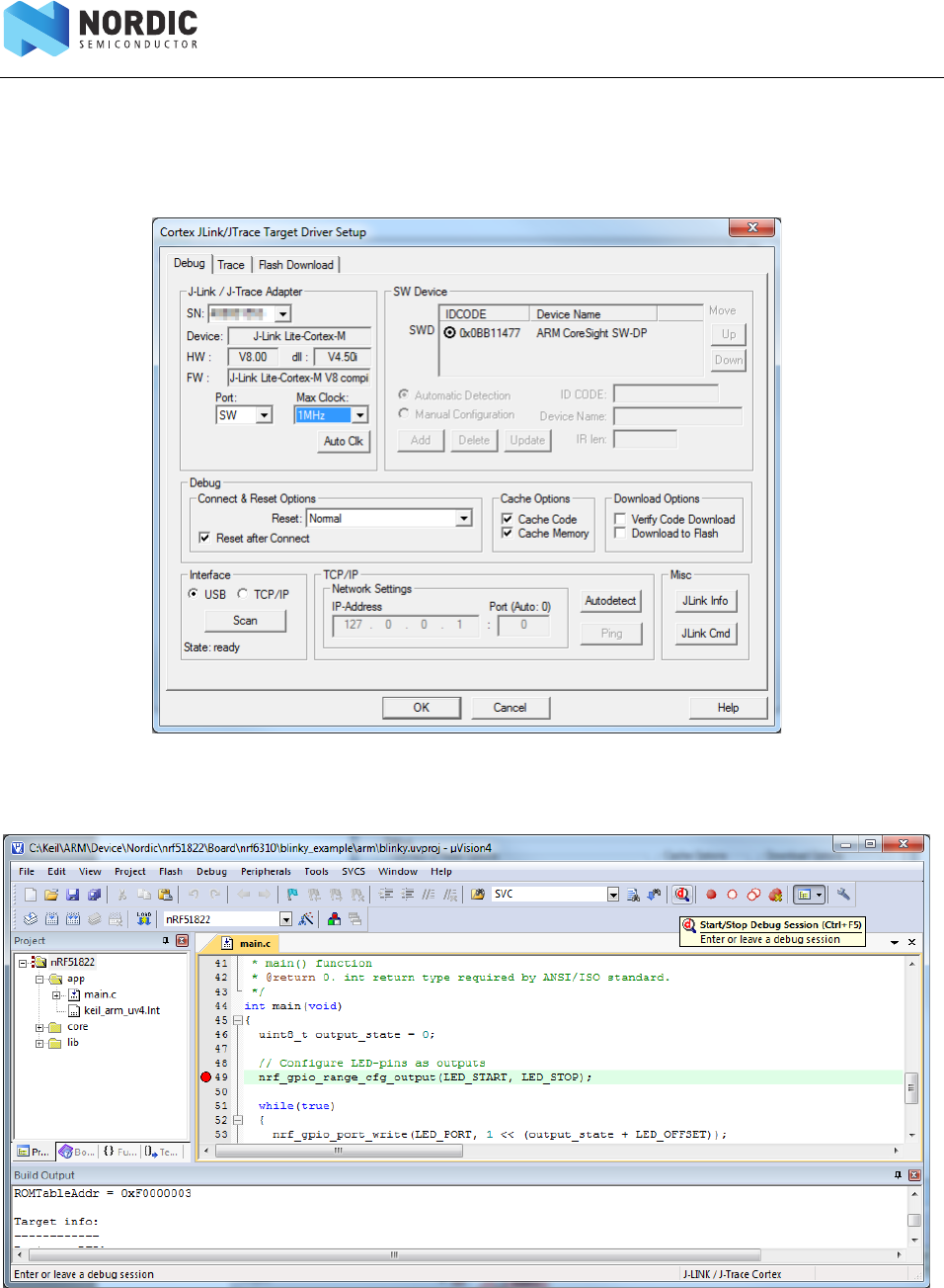
Page 36 of 56
nRF51822 Development Kit User Guide v1.2
7. In the Target driver setup, provide information about debugging protocol and maximum speed.
Select SW in the Port drop-down.
8. In Max Clock the maximum speed for the debugging port cannot be exceeded (1 MHz). A proper
configuration is shown in Figure 26 on page 36.
Figure 26 Target driver setup
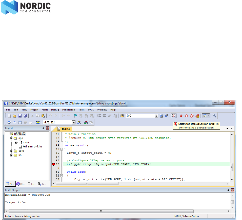
9. Click Start/Stop Debug Session (CTRL+F5) in the Keil IDE to start debugging.
Figure 27 Debugger initiation
Page 37 of 56
nRF51822 Development Kit User Guide v1.2
6.2.4 Limitation when debugging on a chip with a SoftDevice
When a SoftDevice is installed in a device, there are certain limitations when debugging.
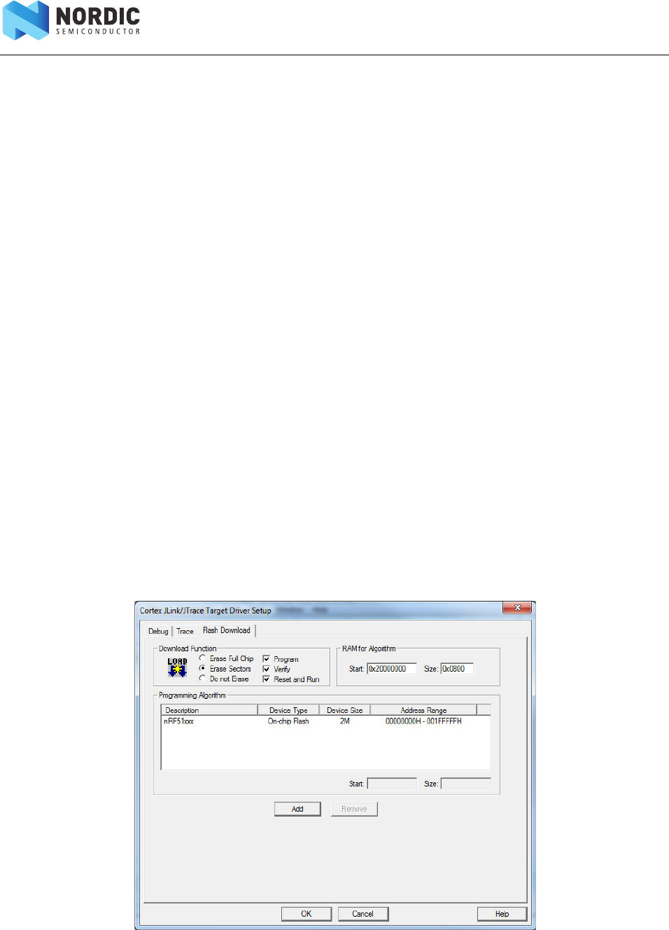
6.2.5 Programming the device
To guarantee the correct functionality of the SoftDevice, the microcontroller includes a Memory Protection
Unit that prevents access to certain resources. The debugger will read this area as 0x0000 (no operation
instruction).
The code memory area occupied by the SoftDevice is write and erase protected. When the SoftDevice is
enabled, the Memory Protection Unit implements a write protection to certain peripherals used by the
protocol stack. Protected peripherals are described in the S110 nRF51822 SoftDevice Specification.Configure
the debugger and compile and link the application code. Download the application using the Keil IDE
download button. To configure and start the download:
1. Select Options for Target in the Project menu.
2. Select the Utilities tab in the Options for Target dialog box.
3. Click Settings.
4. Select the Program check box.
5. Choose Erase Full Chip.
6. Click Add and select the nRF51xxx algorithm from the list to select the programming algorithm
used by Keil IDE.
7. Click Download.
Note: The nRF51xxx algorithm is installed automatically during the SDK installation. This algorithm is
a generic nRF51 series algorithm, which provides download capabilities to all series devices up
to 2 MB of code memory.
Figure 28 Selecting J-Link/J-Trace Cortex
Page 38 of 56
nRF51822 Development Kit User Guide v1.2
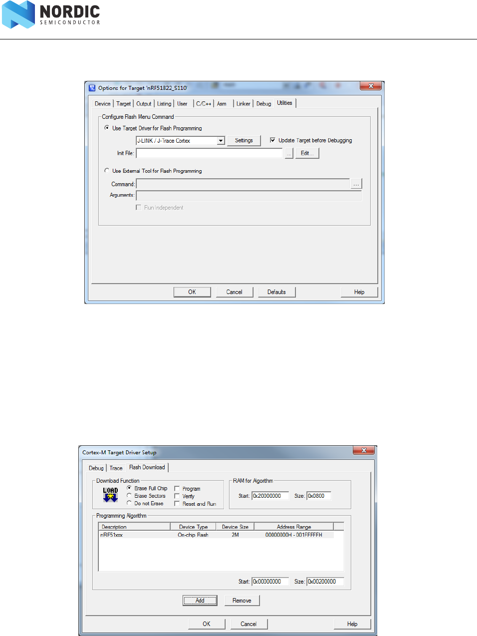
8. In the Utilities tab, select Use Target Driver for Flash Programming.
9. Choose the available debugger from the list as shown in Figure 29.
Figure 29 Debugger selection
6.2.6 Erasing the device
The code memory area available for the user application can be erased by doing the following:
1. In the Target options dialog select the Utilities tab.
2. Click Settings and select Erase Full Chip.
3. Uncheck Program and Verify.
A normal download procedure will erase the device application code memory area.
Figure 30 Erasing
Note: To erase the whole device, including the SoftDevice, refer to section 6.1.3 on page 28 for
instructions.
Page 39 of 56
nRF51822 Development Kit User Guide v1.2
7 Debugging the nRF51822
For debugging with SEGGER J-Link, see Appendix A on page 49. For general information of how to debug
using the Keil µVision IDE, see http://www.keil.com/uvision/debug.asp.
The following steps tell how to configure the debugger in Keil.
1. In the Project menu click Options for Target (CTRL+F7).
2. Select the Debug tab.
3. To enter debugging mode click Start/Stop Debug Session or CTRL+F5.
Figure 31 Start debugging mode
Page 40 of 56
nRF51822 Development Kit User Guide v1.2
7.1 nRF51822 debug features and precautions
This section contains information about the System Viewer Windows and debugging an application when a
readback protected SoftDevice is present.
7.1.1 System Viewer windows
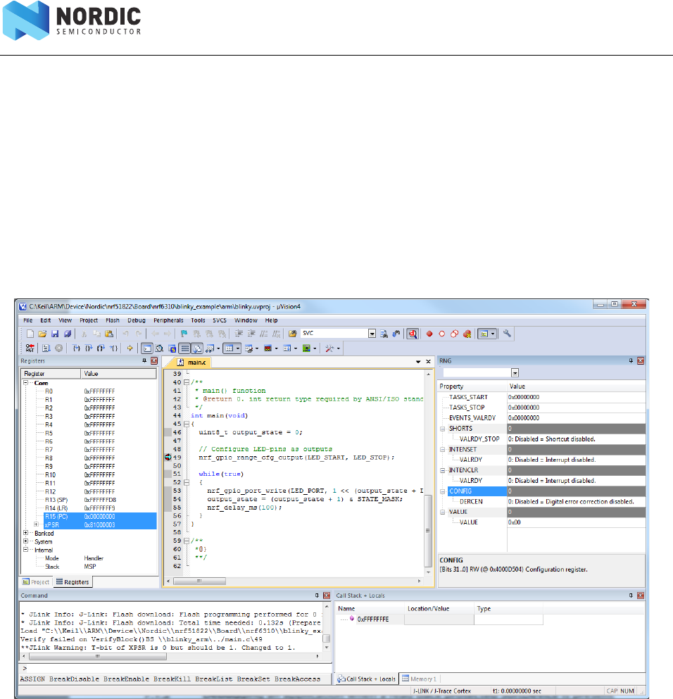
The System Viewer enables you to select device peripherals and see their contents in separate windows. In
the View menu point to System Viewer and select the peripheral you want to see. The peripheral register
values are displayed in their respective pane in Keil, as seen in Figure 32. More information on System Viewer
can be found at: http://www.keil.com/uvision/db_view_sysview.asp.
Figure 32 System Viewer window of the RNG peripheral
Page 41 of 56
nRF51822 Development Kit User Guide v1.2
7.1.2 Debugging an application when a readback protected SoftDevice is present
Debugging applications with a SoftDevice present behaves as described in http://www.keil.com/uvision/
debug.asp, except when the program counter is in Region 0 on a SoftDevice with readback protection
enabled. Code words from addresses in the protected area will always return zero to the debugger.
Any values in peripheral registers that are restricted or blocked by the SoftDevice will be invisible to the
debugger as well. Information on the SoftDevice configuration and memory resource mapping can be
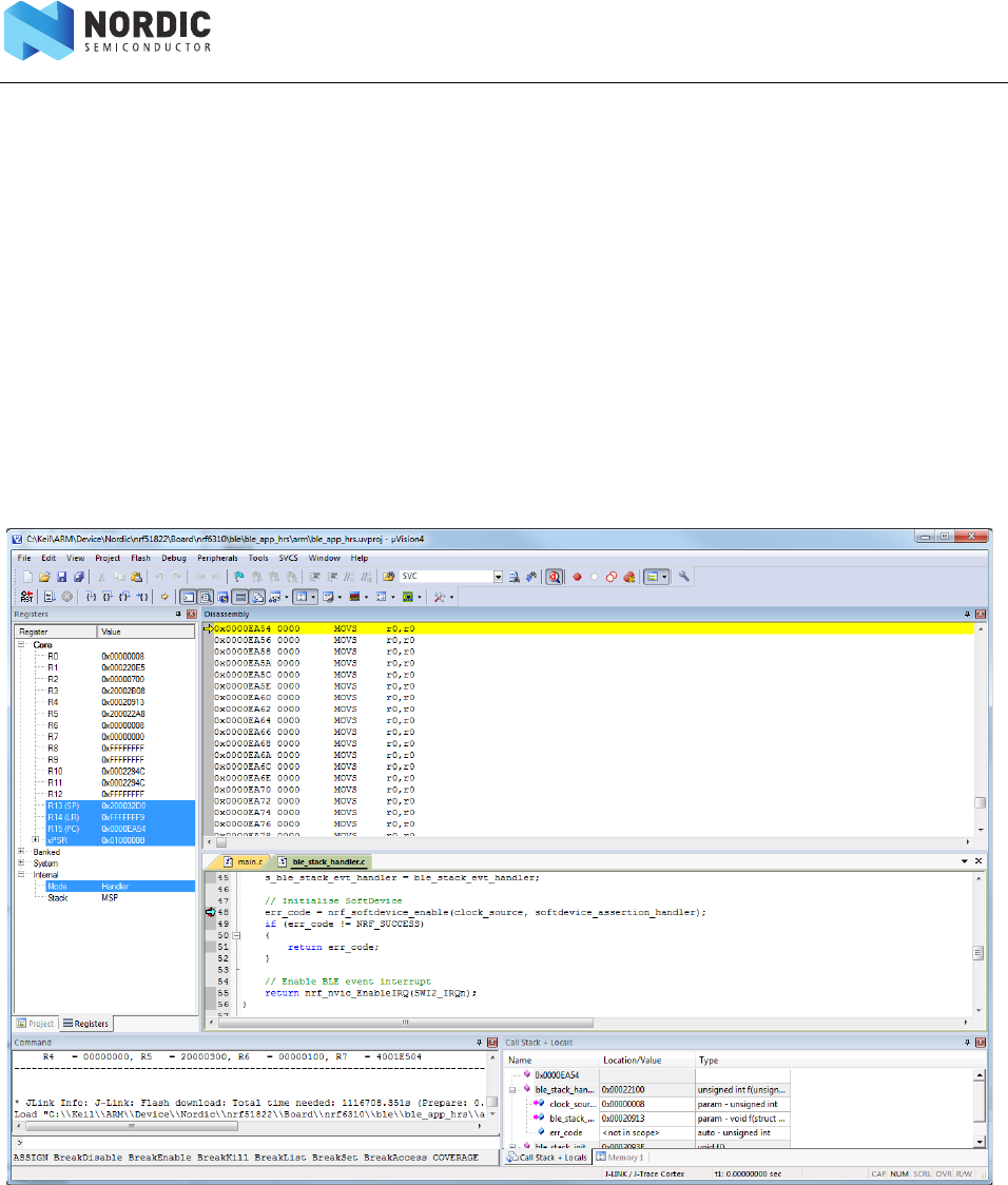
found in the S110 nRF51822 SoftDevice Specification.
Note: Avoid single stepping to the protected area. Instead, set the breakpoint right after SVC calls
while debugging and run the application to the actual breakpoint, see Figure 34 on page 42.
The “step over” function (F10) may also be used instead to step over SVC calls to avoid delays
when entering the readback protected area.
Figure 33 Debugger information for a setup with a SoftDevice enabled in the protected area
Page 42 of 56
nRF51822 Development Kit User Guide v1.2
Figure 34 Setup with breakpoint after an SVC call

Page 43 of 56
nRF51822 Development Kit User Guide v1.2
8 Testing the physical layer with Direct Test Mode
The Direct Test Mode (DTM) interface enables you to test the RF parameters/performance of the Bluetooth
low energy radio design. It can be used for performance testing, tuning your prototypes, and compliance
testing. This interface is compliant with the description in the Bluetooth Specification, Version 4.0, Volume 6,
Part F.
DTM testing requires that you program the chip with the DTM application that is delivered with the nRF51
SDK as described in section 8.2 on page 45.
The DTM UART setting features:
•1 stop bit
• 8 data bits
• 19200 baud rate
• No flow control (meaning no RTS/CTS)
•No parity
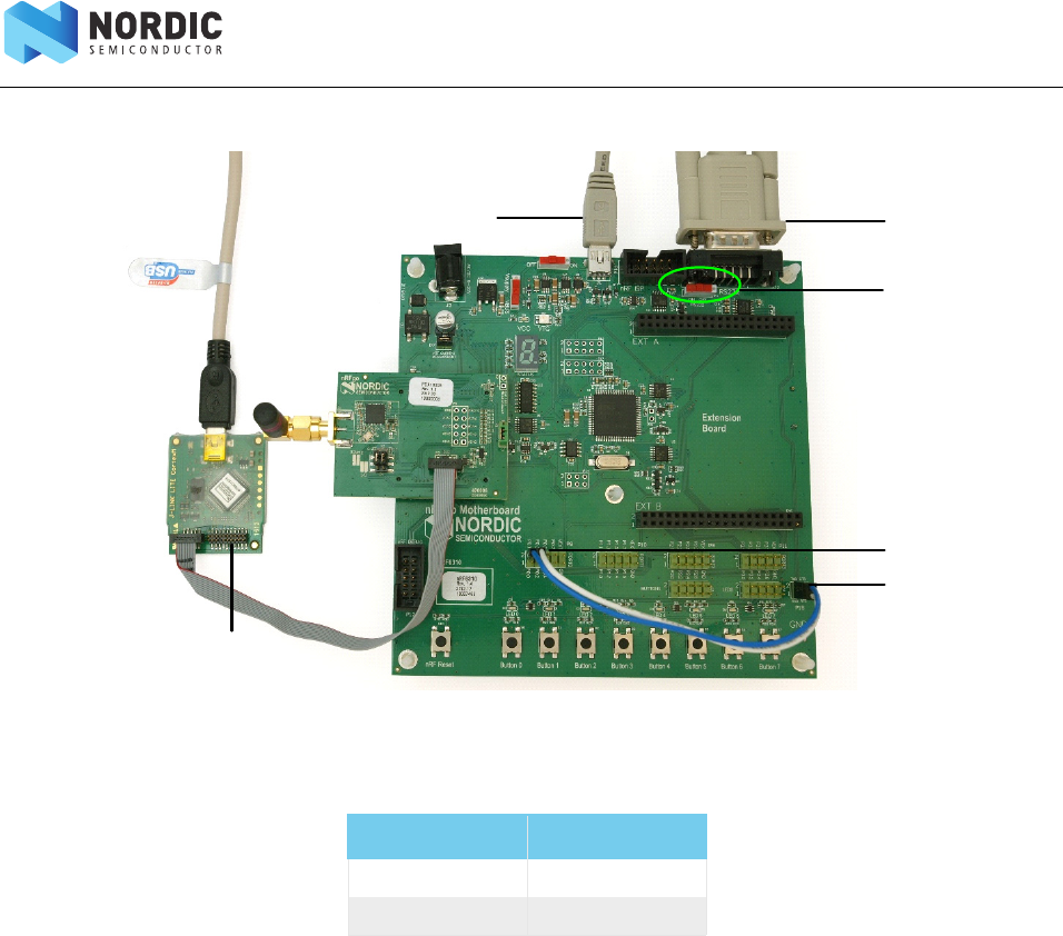
8.1 Kit setup for UART
The Direct Test Mode is accessed through the UART on the nRF51822 module. The following steps show
how to get set up for DTM testing.
1. Mount one of the nRF51822 modules (either PCA10004 or PCA10005) onto the nRFgo
Motherboard.
2. Connect a double cable, or two single cables, between P15 and P8 on the Motherboard as shown
in Figure 35. The UART data pins RXD and TXD will be present on the I/O port pins P0.1 and P0.3 as
seen in Table 7 on page 44. Make sure the RXD/TXD labels match for each wire. This matches the
default setting in the SDK project ble_app_dtm.
3. The RS232 header (P15) is connected to the RS232 serial port interface (J2) through a RS232
converter. Connect a serial cable from RS232 to the serial port on your computer. Make sure S11 is
switched to ON.
4. Connect the Motherboard to your computer using a USB cable.
5. Connect the J-Link Lite CortexM-9 to the nRF51822 module with a 10 pin connector. The USB
cable connects the J-Link Lite CortexM-9 to your computer.
You are now ready to begin testing with Direct Test Mode in nRFgo Studio.
Page 44 of 56
nRF51822 Development Kit User Guide v1.2
Figure 35 UART setup for DTM
Table 7 UART setup
The DTM is designed for use with Bluetooth test equipment. If you don't have a Bluetooth tester you can
access the interface using this Development Kit and nRFgo Studio to run the tests.
Note: In nRFgo Studio, the Program button under Direct Test Mode UART Interface will not work on
the nRF51 platform.
P8 P15
P0.1 TXD
P0.3 RXD
UART
S11
P15
P8
USB
J-Link Lite CortexM
Page 45 of 56
nRF51822 Development Kit User Guide v1.2
8.2 Programming the nRF51822 module with DTM
The nRF51822 module has to be programmed with the DTM application found in the nRF51 SDK. This
application is provided with its source code and needs to be compiled using Keil.
1. Locate the DTM application project found under <Keil path>
\ARM\Device\Nordic\nrf51822\Board\nrf6310\ble\ble_app_dtm\arm.
2. Open the DTM project in Keil µVision by double clicking the ble_app_dtm.uvproj file.
3. Click the Build icon or press F7 to build the project.
4. Only one SEGGER device should be connected to your computer. Make sure it is also connected to
the nRF51822 development module to ensure the program is downloaded to the correct target.
5. Go to the Flash menu and click Download to load the program (or click the Load icon).
You are now ready to start DTM testing either using the Direct Test Mode UART interface included in nRFgo
Studio or connecting 3rd party equipment.
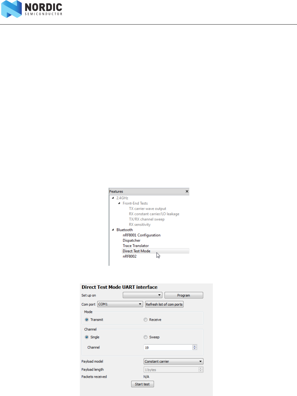
8.3 DTM testing using nRFgo Studio
Select Direct Test Mode in the Feature pane underneath Bluetooth to start the Direct Test Mode UART
interface in nRFgo Studio.
Note: Set up on and Program are not functional when testing on the nRF51 platform.
For details on how to use the Direct Test Mode UART interface see the nRFgo Studio help file (or press F1
when in Studio).

Page 46 of 56
nRF51822 Development Kit User Guide v1.2
9 Software Development Kit
The nRF51 Software Development Kit (SDK) enables you to develop applications for the following protocol
stacks:
•Bluetooth low energy (using the S110_nRF51822 SoftDevice)
• Proprietary 2.4 GHz, including Nordic's Gazell protocol
• Non-concurrent combinations of Bluetooth low energy and proprietary 2.4 GHz
9.1 Installing the nRF51 SDK
The nRF51 SDK is a part of the DK downloadable content available from your My Page account, see section
2.2 on page 5. The SDK is downloaded as a MSI file (a windows installer) and is installed by running the
application. When installing the SDK you can select: Keil MDK Support, Master Control Panel, and/or Custom
install.
•Keil MDK support - installs Keil µVision example project files, the code memory
programming algorithm for the J-Link debugger, and the Nordic nRF51 series device
database file for Keil.
•Custom install - installs a software archive to a customized location.
•nrfjprog - installs a command line programming interface to be used with SEGGER
debuggers.
Note: The Keil MDK Support option will only be available if you already have the Keil MDK toolchain
installed.

Page 47 of 56
nRF51822 Development Kit User Guide v1.2
10 Troubleshooting
The nRF51822 device on the PCA10004/5 does not respond when I try to contact it. What has
happened?
Verify that the jumper on connector K1 on the nRF51822 module is set in the position Pin 2 and Pin 3.
When I connect multiple SEGGER J-Link debugger boards to my computer, μVision does not
recognize them correctly.
This is a known limitation with µVision in MDK v4.53 or earlier that is fixed in later versions. Upgrade to
version 4.54 or later.
The debugger doesn’t work.
Please refer to section 4.2.1 on page 15.
On my 32 bit Windows XP machine, I get an error message with code 2908 when reinstalling
either the nRF514 or nRF518 SDK.
Installing or reinstalling either the nRF518 SDK or the nRF514 SDK after the nRF518 SDK has been
uninstalled will cause error message code 2908 during installation. Use the Task manager (Ctrl+Shift+Esc)
to end the task nRF514/8 SDK Setup. Drivers included in nRF518 will still be installed (if not already
installed).
The debugger seems to freeze while debugging.
If running a SoftDevice that has been programmed with the “Lock SoftDevice from Read back” enabled (see
section section 6.1 on page 27, the debugger will halt while stepping to an SVC instruction. You should set
the breakpoint after the SVC instruction and run the application to the breakpoint, or step over any SVC
instructions. See section 7.1.2 on page 41 for more details.
I have a problem sending/receiving data using the USB to UART bridge.
In order to use the USB to UART bridge the software on nRF51822 has to enable flow control. When
reconnecting the PCA10000 (using the USB cable) the terminal program running on your computer has to
be restarted (you should wait for it to end before disconnecting). Otherwise it locks up the serial port and
the terminal.
Software gets out of sync while debugging.
Setting/modifying breakpoints on a running system using the SEGGER debugger will halt the CPU, which
may result in software that is out of sync. You should avoid setting breakpoints while the system is running.
The debugger does not halt on breakpoints.
Some Keil projects in the SDK have Optimization level 3 (-03) and Optimize for time checked. If you are
debugging an application with these settings, your breakpoint set might have no effect.
1. Press Alt+F7 to open the Target options dialog.
2. Select C/C++.
3. Select Optimization level 0 from the scroll down list.
4. Uncheck Optimize for time.

Page 48 of 56
nRF51822 Development Kit User Guide v1.2
The debugger is not able to detect my nRF51 device after I have downloaded my firmware.
If the nRF51 device goes to SystemOff too soon after reset, it will have a problem communicating with the
J-Link debugger. You can recover using the Recover button in nRFgo Studio.
1. Cycle the power to the nRF51 chip before you start the Recover application.
Note: The Recover function will erase all application firmware apart from the one that comes pre-
programmed on the chip.
The drop-down menu in the Master Control Panel doesn’t display any serial numbers. What has
happened?
Verify that the Master Control Panel software and the drivers for Segger OB (JLinkCDCInstaller) have been
installed and that the nRF51 Development Dongle (PCA10000) has been plugged into a USB port on your
computer.
The Master Control Panel connects to the nRF51 Development Dongle (PCA10000) but reports
“No response from master emulator” in the Log?
You haven’t programmed the nRF51 Development Dongle with the Master Emulator Firmware before
starting to use it. See Scan for available Bluetooth low energy devices in section 2 on page 4 for details on
how to program the Master Emulator Firmware.
My project used to work, but after trying out another project using the SoftDevice, it fails.
Ensure that the memory layout in your project matches the memory layout on the chip. See section 6.2.1 on
page 31 on how to set up memory configuration.
Page 49 of 56
nRF51822 Development Kit User Guide v1.2
Appendix A: Installing drivers and configuring KEIL projects for the
SEGGER debugger
This appendix describes the steps for installing the software and using the SEGGER J-Link Lite debugger
with Keil µVision for nRF51 series devices, based on J-Link software version 4.52b or later.
Prerequisite
You need Keil µVision with ARM-MDK that you have tested to be working with MDK version 4.54.
Note: All projects in the nRF518SDK are preset to work with the SEGGER debugger. Only the
following step Download and install SEGGER drivers is needed.
Download and install SEGGER drivers
1. Download the latest SEGGER J-Link software and documentation pack from
http://www.segger.com/jlink-software.html.
2. Download and run the J-Link Software and documentation pack for Windows from
http://www.segger.com/jlink-software.html. The serial number from your SEGGER J-Link hardware
is needed, see Figure 37 on page 50.
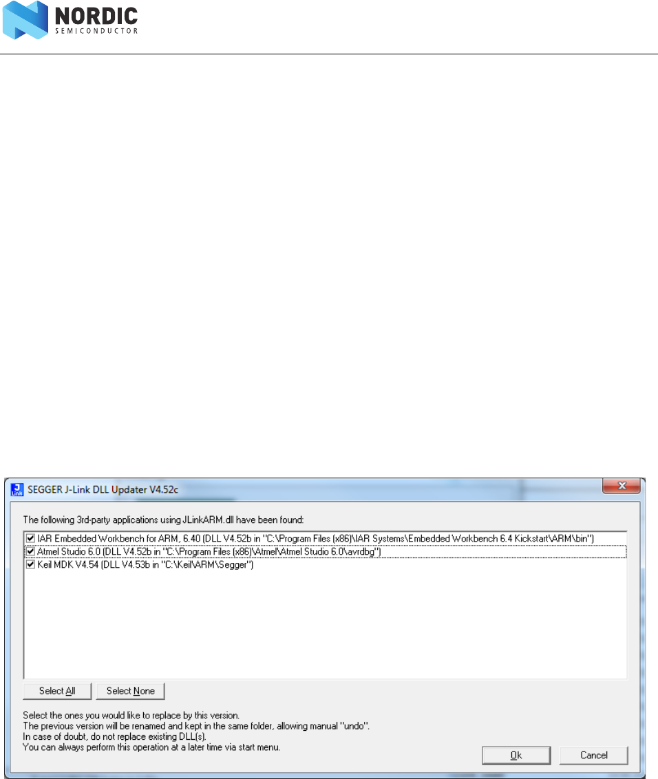
3. During installation you will be prompted to select the IDE that you want updated with the latest
SEGGER DLLs. Check the box for Keil MDK and any other IDEs you want to use with SEGGER.
Figure 36 IDEs selected for updating to the latest SEGGER DLLs
Page 50 of 56
nRF51822 Development Kit User Guide v1.2
4. Go to http://www.segger.com/IDE_Integration_Keil.html#knownproblems for MDK v4.54.
Download JL2CM3 and copy it to <keil>/ARM/Segger. This patch is necessary for the SEGGER
debugger to work.
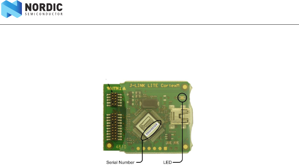
5. Plug in the J-Link Lite CortexM-9 module with USB cable. The LED will blink while the driver
installation occurs. Wait until the LED is continuously lit
Figure 37 J-Link Lite CortexM-9 serial number location
Page 51 of 56
nRF51822 Development Kit User Guide v1.2
Configuring KEIL projects for SEGGER debugger for first time use
Create JLinkSettings.ini file with the contents shown in Figure 43 on page 54. The file JLinkSettings.ini
should be saved in the same folder as Keil µVision project (uvproj) file.
1. Double-click an example project file to open the Keil µVision IDE.
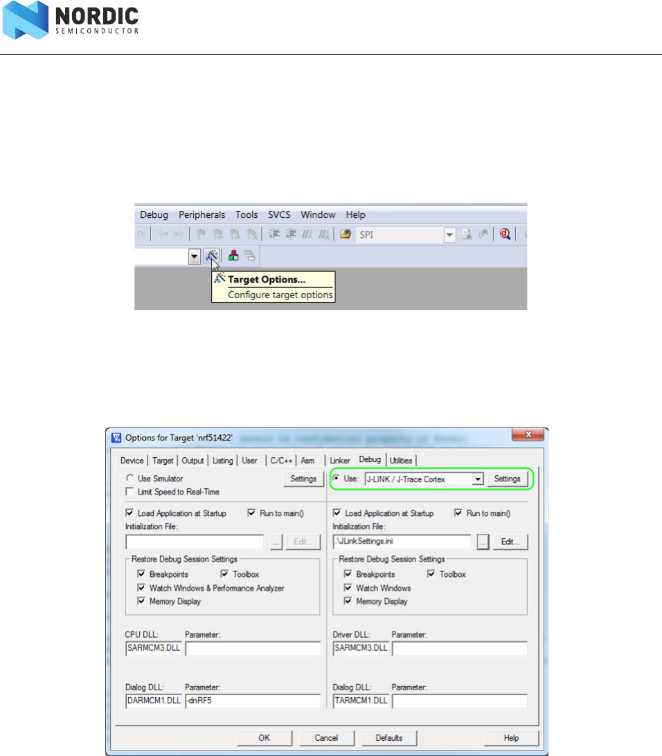
2. Click Target Options on the toolbar or click Project menu and select Options for Target
Figure 38 Keil Target configuration
3. Under the Debug tab in the Use list, select J-LINK / J-Trace Cortex option as shown in Figure 39.
4. Click Settings as shown in Figure 39. Both the SEGGER Control Panel and the Keil Target Driver
Setup will open.
Figure 39 Selecting J-Link debugger in Keil
Page 52 of 56
nRF51822 Development Kit User Guide v1.2
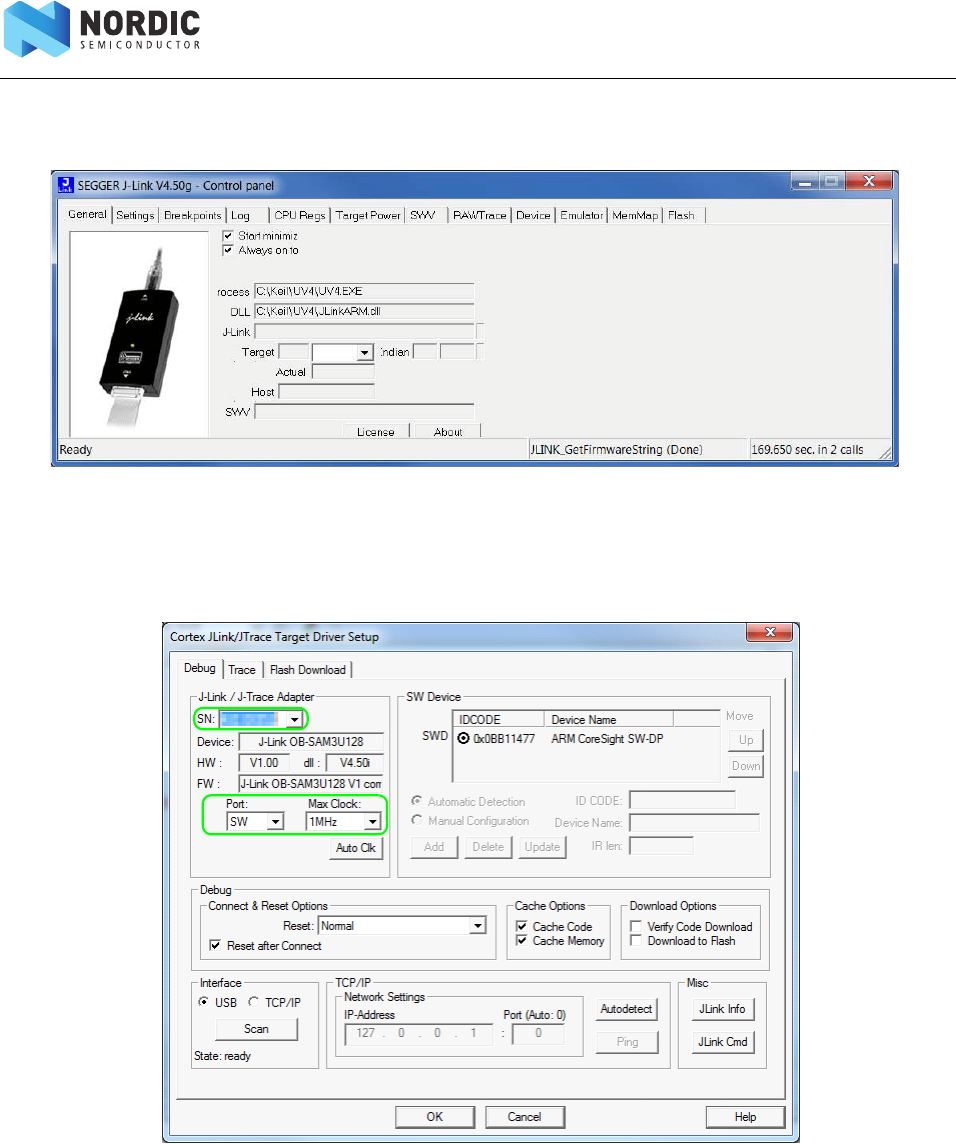
Note: If the SEGGER J-Link Lite firmware requires an update you will be prompted with the message
“A new firmware version is available for the connected emulator”. In this case, click OK.
Figure 40 SEGGER control panel
5. Click the Debug tab shown in the figure. Set Port to SW and Max Clock to 1 MHz, as shown in
Figure 41. Make sure that SN and IDCODE are populated properly and click OK.
Figure 41 Debug settings
6. Select the J-Link device for target programing.
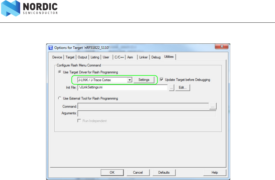
Page 53 of 56
nRF51822 Development Kit User Guide v1.2
Figure 42 Flash settings
7. If the J-Link serial number appears in the SN field, the device is properly installed. The default
settings can be accepted by clicking OK, closing both the SEGGER Control Panel and Keil target
Driver Setup.
Page 54 of 56
nRF51822 Development Kit User Guide v1.2
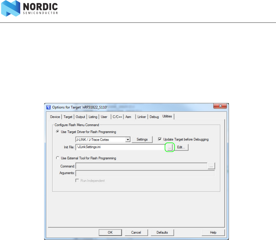
JLinkSettings.ini file
While debugging with a SoftDevice, change AllowSimulation = 1 to AllowSimulation = 0 in your default
JLinkSettings.ini file under your project.
1. Enter the utilities settings from KEIL target options (ALT+F7) and click the ... button to select the
JLinksettings.ini file.
2. Click Edit and change the AllowSimulation as specified above.
Figure 43 Locating JLinkSettings.ini
Page 55 of 56
nRF51822 Development Kit User Guide v1.2
Liability disclaimer
Nordic Semiconductor ASA reserves the right to make changes without further notice to the product to
improve reliability, function or design. Nordic Semiconductor ASA does not assume any liability arising out
of the application or use of any product or circuits described herein.
Life support applications
Nordic Semiconductor’s products are not designed for use in life support appliances, devices, or systems
where malfunction of these products can reasonably be expected to result in personal injury. Nordic
Semiconductor ASA customers using or selling these products for use in such applications do so at their
own risk and agree to fully indemnify Nordic Semiconductor ASA for any damages resulting from such
improper use or sale.
Contact details
For your nearest dealer, please see http://www.nordicsemi.com.
Information regarding product updates, downloads, and technical support can be accessed through your
My Page account on our homepage.
Main office:
Phone: +47 72 89 89 00
Fax: +47 72 89 89 89
Otto Nielsens veg 12
7052 Trondheim
Norway
Mailing address: Nordic Semiconductor
P.O. Box 2336
7004 Trondheim
Norway
Page 56 of 56
nRF51822 Development Kit User Guide v1.2
Revision history
ARM statement
Keil, μVision, and Cortex are trademarks of ARM Limited. All other brands or product names are the property of their respective holders.
Date Version Description
February 2013 1.2 Updated minor documentation errors.
January 2013 1.1 Updated content to match v2.0 of the
hardware. Updated the hardware
content in section 5 on page 17,
programming information in section 8
on page 43, and section 9 on page 46.
September 2012 1.0 First release
