PixArt Imaging PAJ2801UA-40 PAJ2801UA-40 Wireless BLE 4.0 Module User Manual PAC7640 Datasheet
PixArt Imaging Inc. PAJ2801UA-40 Wireless BLE 4.0 Module PAC7640 Datasheet
Users Manual

Low Power Heart Rate MonitorLow
Preliminary: This product is still under product development where the product specifications are subjected to change upon product release
1
PixArt Imaging Inc.
Version 0.34 | 29 Jul 2016
PixArt Imaging Inc. http://www.pixart.com
All rights reserved. Any portion in this paper shall not be reproduced, copied, or transformed to any other forms without permission.
PAJ2801UA-40 User’s Manual
Low Power Bluetooth 4.0 Module
PAJ2801UA-40: Low Power Bluetooth 4.0 Module
General Description
PAJ2801UA-40 is a low power and high performance BLE
module with embedded antenna. It integrates all the
needs as a Bluetooth smart device which includes the
maximum of 30 of GPIOs, PWM, I2C, UART, ADC and SPI.
Key Features
Based on PixArt’s PAR2801 BLE SoC
Fully qualified Bluetooth Low Energy 4.0 peripheral
device
Cortex M0 32-bit MCU with max. 32MHz clock rate
Low power and excellent performance 2.4GHz
transceiver with built-in balun
Integrate 1Mbit Flash and 80kB SRAM
2 channel 10-bit SAR ADC
Highly integrated SOC with128kB Flash and 80kB
SRAM
16MHz and 32.768kHz crystal oscillator circuit and
loading capacitors, no external loading capacitors
needed
Quadrature Decoder
DCDC converter, Boost or Buck Mode
Built in 32MHz and 32.768kHz RC oscillator
Communication interface options
Master I2C x2
Master Two/Four-Wire SPI x2
UART x2
Digital peripherals
LED x3
PWM x3
Support Serial Wire (SW) debug mode
Applications
IoT Devices
HID peripherals
Health and Fitness wearable device
Interactive entertainment device
Home and industrial automation
Security/Proximity applications
Key Parameters
Parameter
Value
Max. TX Power
+4 dBm
RX Sensitivity
-93 dBm
Carrier frequency
2402 ~ 2480
Modulation
GFSK
Antenna type
Printed Monopole
DTM TX Current @ 0dBm*
10.0 mA
DTM RX Current*
13.5 mA
Sleep Mode Current
<8 µA
Deep Sleep Mode Current
<3 µA
RF Input Impedance
50 Ω
ROM Size
24 kB
Internal Flash
128 kB
SRAM
80 kB
Supply Voltage
Buck Mode: 1.9~3.6 V
GPIO
30
Operating Temperature, Tj
-20~+85 °C
Module Size
11.5 x 18.0 x 2.6 mm
Measured under DC-to-DC Buck Mode
Ordering Information
PA Number
Module Size
PAJ2801UA-40
11.5 x 18.0 x 2.6 mm
For any additional inquiries, please contact us at
http://www.pixart.com/contact.asp

2
PixArt Imaging Inc.
PixArt Imaging Inc. http://www.pixart.com
All rights reserved. Any portion in this paper shall not be reproduced, copied, or transformed to any other forms without permission.
PAJ2801UA-40 User’s Manual
Low Power Bluetooth 4.0 Module
Version 0.34 |29 Jul 2016
Contents
PAJ2801UA-40: Low Power Bluetooth 4.0 Module ................................................................................................................... 1
General Description ............................................................................................................................................................ 1
Key Features ....................................................................................................................................................................... 1
Applications ........................................................................................................................................................................ 1
Key Parameters ................................................................................................................................................................... 1
Ordering Information .......................................................................................................................................................... 1
List of Figures ........................................................................................................................................................................... 3
List of Tables ............................................................................................................................................................................ 4
1.0 Introduction ................................................................................................................................................................. 5
1.1 Overview ................................................................................................................................................................. 5
1.2 Terminology ............................................................................................................................................................ 5
1.3 Pin Assignment and Signal Description .................................................................................................................... 5
2.0 Mechanical Specifications ............................................................................................................................................ 9
2.1 Mechanical Dimension ............................................................................................................................................ 9
2.2 Module Case Marking .............................................................................................................................................. 9
2.3 Main Board PCB ..................................................................................................................................................... 10
3.0 Design References ...................................................................................................................................................... 11
3.1 Layout Design Guidelines ...................................................................................................................................... 11
4.0 Power States & Sequence .......................................................................................................................................... 12
4.1 Operation Mode .................................................................................................................................................... 12
5.0 System Description .................................................................................................................................................... 13
5.1 ARM Cortes M0 ..................................................................................................................................................... 13
5.2 Bluetooth Low Energy Core ................................................................................................................................... 13
5.3 Radio Transceiver .................................................................................................................................................. 14
5.4 General Purpose ADC ............................................................................................................................................ 14
5.5 Power Management .............................................................................................................................................. 14
6.0 Interfaces ................................................................................................................................................................... 15
6.1 UART ...................................................................................................................................................................... 16
6.2 I2C ......................................................................................................................................................................... 16
6.3 SPI .......................................................................................................................................................................... 16
7.0 End-Product Label ...................................................................................................................................................... 25
Document Revision History .................................................................................................................................................. 176

3
PixArt Imaging Inc.
PixArt Imaging Inc. http://www.pixart.com
All rights reserved. Any portion in this paper shall not be reproduced, copied, or transformed to any other forms without permission.
PAJ2801UA-40 User’s Manual
Low Power Bluetooth 4.0 Module
Version 0.34 |29 Jul 2016
List of Figures
Figure 1. Pin Configuration ...................................................................................................................................................... 5
Figure 2. Module PCB Top View ............................................................................................................................................... 9
Figure 3. Module PCB Bottom View ........................................................................................................................................ 9
Figure 4. Module Case Marking ............................................................................................................................................... 9
Figure 5. Module Placement and Keep-out Region ............................................................................................................... 10
Figure 6. Recommended Module Footprint .......................................................................................................................... 10
Figure 7. Label (Laser Marking) ............................................................................................................................................. 16

4
PixArt Imaging Inc.
PixArt Imaging Inc. http://www.pixart.com
All rights reserved. Any portion in this paper shall not be reproduced, copied, or transformed to any other forms without permission.
PAJ2801UA-40 User’s Manual
Low Power Bluetooth 4.0 Module
Version 0.34 |29 Jul 2016
List of Tables
Table 1. Signal Pins Description ............................................................................................................................................... 6
Table 2. IO Mode Selection ...................................................................................................................................................... 8
Table 3. Code Identification ..................................................................................................................................................... 9
5
PixArt Imaging Inc.
PixArt Imaging Inc. http://www.pixart.com
All rights reserved. Any portion in this paper shall not be reproduced, copied, or transformed to any other forms without permission.
PAJ2801UA-40 User’s Manual
Low Power Bluetooth 4.0 Module
Version 0.34 |29 Jul 2016
1.0 Introduction
1.1 Overview
The PAR2801QN-GH chip is highly integrated with ARM® Cortex®-M0 processor, Bluetooth Low Energy v4.0 baseband
control core, ROM, Flash, Bluetooth Modem, Radio Transceiver, on-chip Balun and digital interfaces for the BLE application.
The Cortex M0 can operate at 32MHz clock rate for heavy thread computing application, and can also operate at lower
clock rate for simple data communication purpose. PAR2801QN-GH has DCDC converter built-in to provide full-solution SoC
for stand-alone applications such as HID and Wearable devices.
1.2 Terminology
Term
Description
GND
Ground
BiDir
Bi-Directional
PWM
Pulse Width Modulation
HID
Human Interface Device
GPIO
General Purpose Input / Output
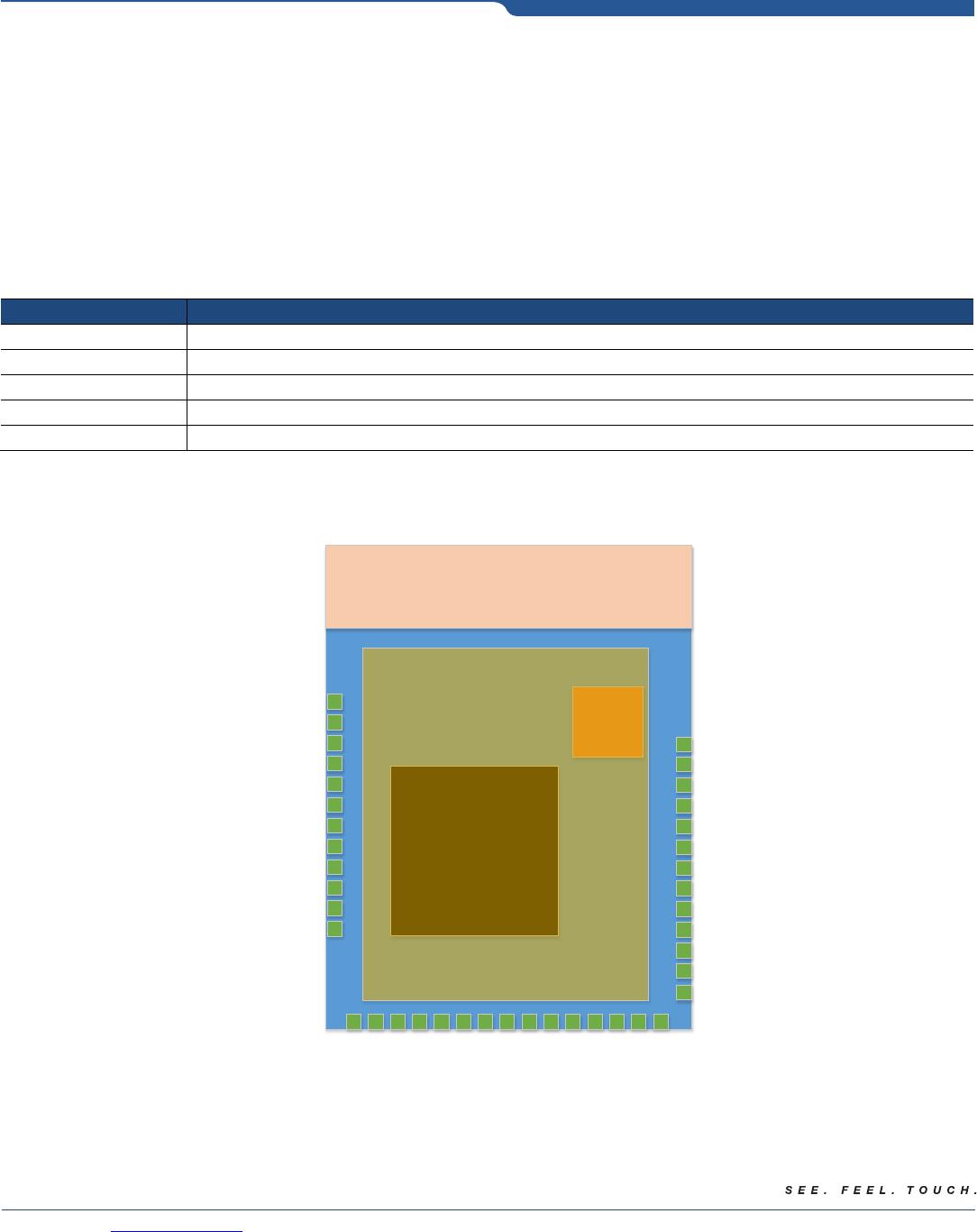
1.3 Pin Assignment and Signal Description
天線淨空區
Antenna keep-out region
XTAL
11.5mm
18mm
P1
P13
P28
P40
PAR2801
Shielding Case
3mm
Figure 1. Pin Configuration

6
PixArt Imaging Inc.
PixArt Imaging Inc. http://www.pixart.com
All rights reserved. Any portion in this paper shall not be reproduced, copied, or transformed to any other forms without permission.
PAJ2801UA-40 User’s Manual
Low Power Bluetooth 4.0 Module
Version 0.34 |29 Jul 2016
Table 1. Signal Pins Description
Pin No.
Signal Name
Type
Description
1
GND
Power
Ground
2
ICE_DATA
BiDir
Serial debug port interface – DATA
GPO
3
ICE_CLK
BiDir
Serial debug port interface – Clock
GPO
4
GPIO27
BiDir
GPIO, PWM2, or LED2
I2C: Data IO, as I2C_SDA0
UART: UART_TXD0
5
GPIO26
BiDir
GPIO, PWM0, or LED0
I2C:Clock output, as I2C_SCL0,
UART: UART_RXD0
6
GPIO25
BiDir
GPIO, Key_T2, PWM1, or LED1
UART: UART_RTS0
7
GPIO24
BiDir
GPIO, Key_T1, PWM2, or LED2
UART: UART_CTS0
8
GPIO23
BiDir
GPIO, or Key_Z2
I2C: Data IO,as I2C_SDA1
UART: UART_TXD1
9
GPIO22
BiDir
GPIO, or Key_Z1
I2C:Clock output, I2C_SCL1
UART: UART_RXD1
10
GPIO21
BiDir
GPIO, PWM1, or LED1
11
GPIO20
BiDir
GPIO, PWM2, or LED2
UART: UART_TXD0
12
GPIO19
BiDir
GPIO, PWM0, or LED0
UART: UART_RXD0
13
GPIO18
BiDir
GPIO, PWM1, or LED1
UART: UART_RTS0
14
GPIO17
BiDir
GPIO, PWM2, or LED2
UART: UART_CTS0
15
GPIO16
BiDir
GPIO, MouseKey_B5, PWM0, or LED0
I2C:Data IO, I2C_SDA1
16
GPIO15
BiDir
GPIO, MouseKey_B4, PWM1, or LED1
I2C:Clock output, I2C_SCL1
17
GPIO14
BiDir
GPIO, MouseKey_CPI, PWM2, or LED2
18
VDDIO
Power
Power for IO
19
GPIO13
BiDir
GPIO, MouseKey_Middle
20
GPIO12
BiDir
GPIO, MouseKey_Right
21
GPIO11
BiDir
GPIO, MouseKey_Left
22
GPIO10
BiDir
GPIO, Motion_Wake_Up as motion detect for external sensor, Active_Low
23
GPIO9
BiDir
GPIO
SPI4W: Master, Data output, SPI_DO

7
PixArt Imaging Inc.
PixArt Imaging Inc. http://www.pixart.com
All rights reserved. Any portion in this paper shall not be reproduced, copied, or transformed to any other forms without permission.
PAJ2801UA-40 User’s Manual
Low Power Bluetooth 4.0 Module
Version 0.34 |29 Jul 2016
Pin No.
Signal Name
Type
Description
24
GPIO8
BiDir
GPIO
SPI4W:Master, Chip Select, SPI_CSN
SPI3W:Master, Chip Select, SPI_CSN
25
GPIO7
BiDir
GPIO
SPI4W:Master, Data input, SPI_DI
SPI3W:Master, Data IO, SPI_DIO
I2C:Data IO, I2C_SDA0
26
GPIO6
BiDir
GPIO
SPI4W:Master, Clock output, SPI_CLK
SPI3W:Master, Clock output, SPI_CLK
I2C:Clock output, I2C_SCL0
27
GPIO5
BiDir
GPIO
SPI4W: Master, Data output, SPI_DO_1
I2C:Data IO, I2C_SDA1
UART: UART_TXD0
28
GPIO4
BiDir
GPIO
SPI4W: Master, Chip Select, SPI_CSN_1
I2C: Clock output, I2C_SCL1
UART: UART_RXD0
29
GPIO3
BiDir
GPIO
SPI4W:Master, Data input, SPI_DI_1
UART: UART_RTS0
30
GPIO2
BiDir
GPIO, PWM0, or LED0
SPI4W: Master, Clock output, SPI_CLK_1
UART: UART_CTS0
31
GPIO1
BiDir
GPIO, PWM1, or LED1
Analog Input_1
I2C:Data IO, I2C_SDA1
UART: UART_TXD1
32
GPIO0
BiDir
GPIO, PWM2, or LED2
Analog Input_0
I2C: Clock output, I2C_SCL0
UART: UART_RXD0
33
GND
Power
Ground
34
DVDD2
Power
DCDC power output
35
VBAT
Power
Input Power pin, connect to battery or external power source. Recommend to
add de-coupling cap, 10uF. Keep PCB trace as short and as wide as possible.
36
GND
Power
Ground
37
XTAL1_32k
In
Crystal input for 32.768kHz XTAL
38
XTAL2_32k
Out
Crystal output for 32.768kHz XTAL
39
RF_RSTB
In
Active Low signal for HW reset. Need to add a series Resistor at VDDIO power
domain to establish RC POR circuit (R=100k, C= 100nF).
40
GND
Power
Ground

8
PixArt Imaging Inc.
PixArt Imaging Inc. http://www.pixart.com
All rights reserved. Any portion in this paper shall not be reproduced, copied, or transformed to any other forms without permission.
PAJ2801UA-40 User’s Manual
Low Power Bluetooth 4.0 Module
Version 0.34 |29 Jul 2016
Table 2. IO Mode Selection
GPIO_#
0
1
2
3
4
5
GPIO0
GPIO0
Analog Input 0
I2C_SCL1
UART_RXD1
PWM2/LED2
GPIO1
GPIO1
Analog Input 1
I2C_SDA1
UART_TXD1
PWM1/LED1
GPIO2
GPIO2
M_SPICK_1
UART_CST0
PWM0/LED0
GPIO3
GPIO3
M_SPIDI_1
UART_RTS0
GPIO4
GPIO4
M_SPICSN_1
I2C_SCL1
UART_RXD0
GPIO5
GPIO5
M_SPIDO_1
I2C_SDA1
UART_TXD0
GPIO6
GPIO6
M_SPICK_0
M_SPICK_0
I2C_SCL0
GPIO7
GPIO7
M_SPIDI_0
M_SPI_IO_0
I2C_SDA0
GPIO8
GPIO8
M_SPICSN_0
M_SPICSN_0
GPIO9
GPIO9
M_SPIDO_0
GPIO10
GPIO10
MOTION_Wake_UP
GPIO11
GPIO11
Mouse Key (BL)
GPIO12
GPIO12
Mouse Key (BR)
GPIO13
GPIO13
Mouse Key (BM)
GPIO14
GPIO14
Mouse Key (CPI)
PWM2/LED2
GPIO15
GPIO15
Mouse Key (B4)
I2C_SCL1
PWM1/LED1
GPIO16
GPIO16
Mouse Key (B5)
I2C_SDA1
PWM0/LED0
GPIO17
GPIO17
UART_CST0
PWM2/LED2
GPIO18
GPIO18
UART_RTS0
PWM1/LED1
GPIO19
GPIO19
UART_RXD0
PWM0/LED0
GPIO20
GPIO20
UART_TXD0
PWM2/LED2
GPIO21
GPIO21
PWM1/LED1
GPIO22
GPIO22
Mouse Key (Z1)
I2C_SCL1
UART_RXD1
GPIO23
GPIO23
Mouse Key (Z2)
I2C_SDA1
UART_TXD1
GPIO24
GPIO24
Mouse Key (T1)
UART_CST0
PWM2/LED2
GPIO25
GPIO25
Mouse Key (T2)
UART_RTS0
PWM1/LED1
GPIO26
GPIO26
I2C_SCL0
UART_RXD0
PWM0/LED0
GPIO27
GPIO27
I2C_SDA0
UART_TXD0
PWM2/LED2
ICE - CLK
ICE - CLK
PWM1/LED1
ICE - SDA
ICE - SDA
PWM0/LED0
9
PixArt Imaging Inc.
PixArt Imaging Inc. http://www.pixart.com
All rights reserved. Any portion in this paper shall not be reproduced, copied, or transformed to any other forms without permission.
PAJ2801UA-40 User’s Manual
Low Power Bluetooth 4.0 Module
Version 0.34 |29 Jul 2016
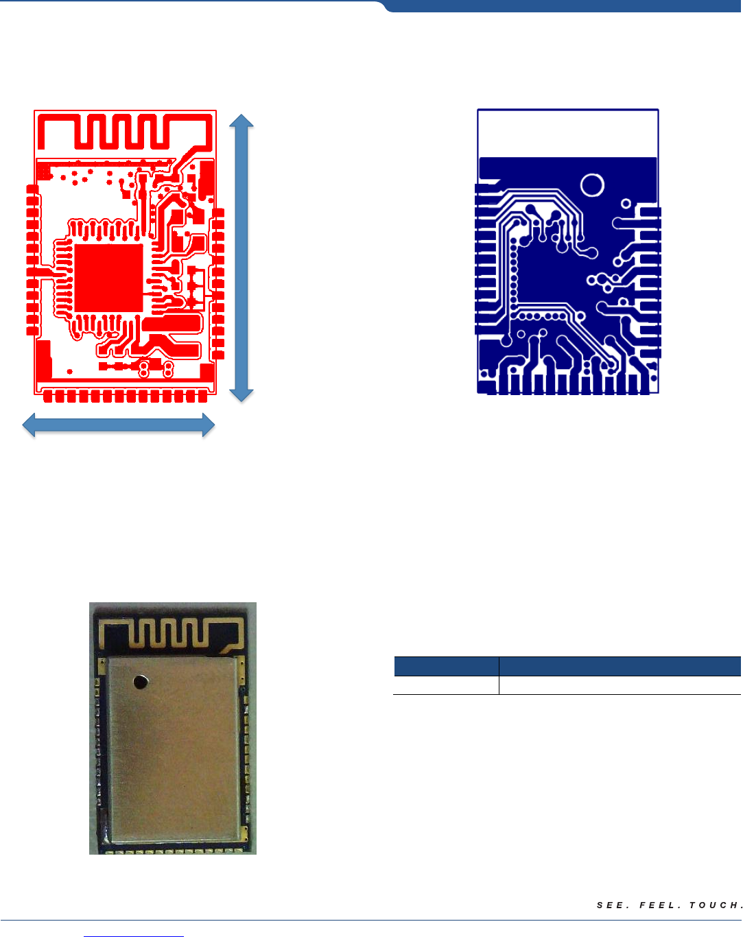
2.0 Mechanical Specifications
2.1 Mechanical Dimension
18mm
11.5mm
Figure 2. Module PCB Top View
Figure 3. Module PCB Bottom View
2.2 Module Case Marking
Refer to Figure 4 for the code marking location on the module case.
Figure 4. Module Case Marking
Table 3. Code Identification
Marking
Description
XXXX
PixArt Code
10
PixArt Imaging Inc.
PixArt Imaging Inc. http://www.pixart.com
All rights reserved. Any portion in this paper shall not be reproduced, copied, or transformed to any other forms without permission.
PAJ2801UA-40 User’s Manual
Low Power Bluetooth 4.0 Module
Version 0.34 |29 Jul 2016
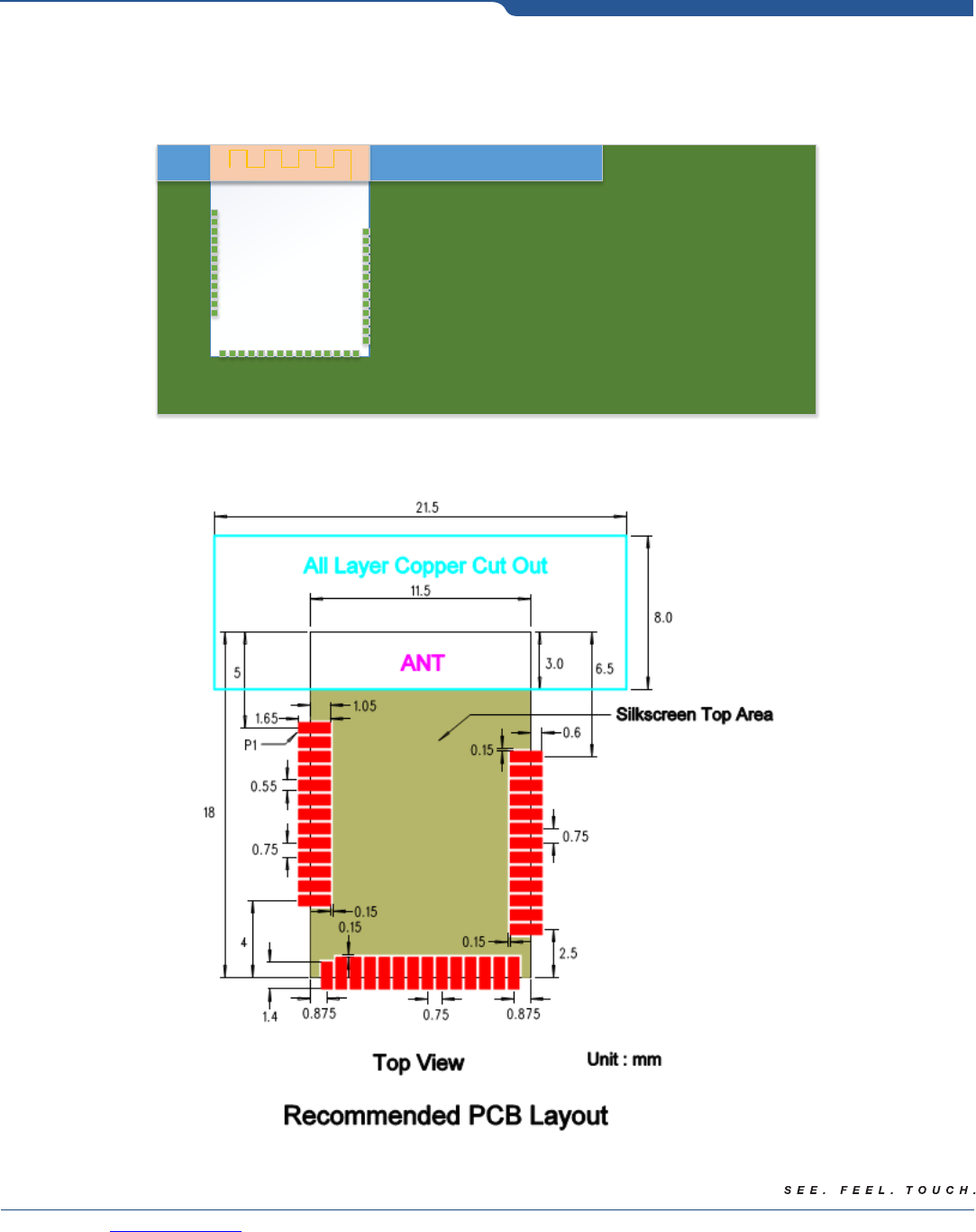
2.3 Main Board PCB
The Figure 7 describes the module placement on the Main board PCB. Do ensure that no user’s hand or metal screw is over
the antenna area. The main board also need to conserve a keep-out region which is at least 5mm surrounding the module
antenna region, and no trace, power and ground in the antenna keep-out region is allowed.
Main Board PCB
Antenna Keep-out Region
Figure 5. Module Placement and Keep-out Region
Figure 6. Recommended Module Footprint

11
PixArt Imaging Inc.
PixArt Imaging Inc. http://www.pixart.com
All rights reserved. Any portion in this paper shall not be reproduced, copied, or transformed to any other forms without permission.
PAJ2801UA-40 User’s Manual
Low Power Bluetooth 4.0 Module
Version 0.34 |29 Jul 2016
3.0 Design References
3.1 Layout Design Guidelines
Precaution: PCB layout is extremely important to minimize parasitical capacitance and line inductance.
The following layout guidelines are recommended to achieve optimum performance.
1. Place ceramic bypass capacitors near the input/output pins.
2. All feedback signals must go through the regulator capacitors first.
3. Place the crystal and its components close to the oscillator side and near the oscillator pins.
4. Ensure that the ground plane under the module, oscillator and its components are in good quality.
5. Avoid long connections to the crystal and also to the load capacitor which may create a large loop on the PCB.
6. Do not route any digital-signal lines under the module, antenna keep-out region and crystal area.
7. Keep other digital signal lines, especially clock lines and frequently switching signal lines, as far away from the module
as possible.

12
PixArt Imaging Inc.
PixArt Imaging Inc. http://www.pixart.com
All rights reserved. Any portion in this paper shall not be reproduced, copied, or transformed to any other forms without permission.
PAJ2801UA-40 User’s Manual
Low Power Bluetooth 4.0 Module
Version 0.34 |29 Jul 2016
4.0 Power States & Sequence
4.1 Operation Mode
State
Functional Description
Power Down
All power supplies are off except I/O for pin wake-up. All clocks are gated.
System can be woken up by configured external pin. When it happens, PAR2801 resets from boot-up
state.
Sleep
Active clocks (16MHz or 32MHz) are off, and the sleep clock remain working. Certain engines’ power
are off.
Two types of sleep modes are provided in PAJ2801. When CPU uses 16MHz crystal clock together
with Bluetooth, it follows Bluetooth sleep mode aligning to connection interval. When CPU uses
internal 32MHz RC clock, it can set CPU sleep mode independently and woken up by timer or
Bluetooth interrupts.
Standby
This is the default state after power-up. All clocks are working but the RF is inactive.
TX
This mode is entered when Bluetooth link-layer determines to send transmission packets.
RX
This mode is entered when Bluetooth link-layer determines to receive an incoming packet.

13
PixArt Imaging Inc.
PixArt Imaging Inc. http://www.pixart.com
All rights reserved. Any portion in this paper shall not be reproduced, copied, or transformed to any other forms without permission.
PAJ2801UA-40 User’s Manual
Low Power Bluetooth 4.0 Module
Version 0.34 |29 Jul 2016
5.0 System Description
5.1 ARM Cortes M0
The ARM® Cortex®-M0 processor is the smallest ARM processor available. It provides low power consumption and minimal
code of the processor to enable developers to achieve 32-bit performance. With its friendly architecture, users can develop
applications easily and fast.
PAR2801QN-GH supports dynamic clock technology for various applications ranging from 8MHz to 32MHz. The CPU clock
can be configured to use internal 32MHz RC clock or 16MHz crystal clock. When using RC clock, MCU can run independently
with Bluetooth link-layer and switch on and off at users’ discretion. When using 16MHz crystal clock, it should follow the
working period of Bluetooth. However, the Bluetooth working period can be determined by MCU.
SWD (Serial-Wire Debug) is supported for powerful debug and trace features with two connection pins.
PAR2801QN-GH has 24kB ROM for boot-up and BLE protocol stack, 128kB flash for profile/application, 48kB internal
program SRAM, and 32kB data SRAM.
5.2 Bluetooth Low Energy Core
The Bluetooth Low Energy Core is SIG Qualified. It is fully compliant with Bluetooth Smart v4.0 slave-role controller and
provide qualified feature as below:
1. Bluetooth low energy stack
All layers up to GATT including (PHY, LL, HCI, L2CAP, GAP, SM, ATT/GATT)
2. Slave-Role Link layer
Slave-required PDU types
Encryption/Decryption
3. L2CAP
Slave connection update
Attribute channel
Security channel
4. GAP/ATT/GATT
Mandatory protocols
5. Security Management
Key generation and passing
Automatic security engine
6. DTM
DTM for RF qualification
7. Profile configuration
Initialization
Flexibility and testability

14
PixArt Imaging Inc.
PixArt Imaging Inc. http://www.pixart.com
All rights reserved. Any portion in this paper shall not be reproduced, copied, or transformed to any other forms without permission.
PAJ2801UA-40 User’s Manual
Low Power Bluetooth 4.0 Module
Version 0.34 |29 Jul 2016
5.3 Radio Transceiver
The PAR2801QN-GH integrates high performance 2.4GHz radio transceiver for Bluetooth radio specification. With built-in
on-chip balun, PAR2801QN-GH does not need external balun circuit to minimize BOM. The integrated high efficiency PA
can transmit up to +4dBm RF power for class 2 operation, while the integrated low-IF receiver can provide excellent
sensitivity up to -93dBm and outstanding interference rejection capability.
5.4 General Purpose ADC
The PAR2801QN-GH integrates a low power 10-bit general purpose Analog-to-Digital Converter (GPADC) with 32kHz
sampling rate. For each one shot measurement, it takes 150us for data acquisition. It can operate as a 4-channel ADC by
switching the GPADC input. Two channels for internal Battery Voltage detection (VBAT3V, VBAT1V), while the other two are
configured to monitor GPIO0 or GPIO1. For better accuracy, internal reference voltage calibration is preferred. Sensing
applications as battery monitoring, temperature resister, analog signal sampling could be applied with this GPADC.
5.5 Power Management
The PAR2801QN-GH integrates an power management unit for handheld or wearable devices with DC/DC(Buck or Boost)
converter. No external Schottky diode is needed for minimal layout area. The DC/DC converter transforms battery voltage
to a lower/higher internal voltage with minimal power loss. The DC/DC converter could provide excellent power efficiency
with adaptive loading current setting. The DC/DC converter can be bypassed when the supply voltage drops to the lower
limit of the voltage range, external DC/DC converter is also supported. It can provide power solution for one-cell Lithium-
Ion, one-cell or multi-cell alkaline battery applications where the output voltage is adjustable.
5.5.1 Buck Converter
Higher performance DC/DC Buck converter would bring up better battery life time. To ensure longest battery life, Buck
converter has an optional bypass mode under light load current. The reduction in supply voltage level from a high voltage
to a low voltage reduces the peak power drain from the battery.
5.5.2 GPIO
PAJ2801UA-40 module offer 28 GPIOs and 2 output only ports (ICE_CLK, ICE_DATA). ICE_CLK and ICE_DATA pins should be
make sure that keep Low during PAR2801 booting procedure. ICE_CLK and ICE_DATA could be configured as output pin
after system boot up.
5.5.3 Timer
PAR2801QN-GH provide 4 timers with 32-bit width. Timer0~Timer4 are running with 32.768kHz clock from 32.768kHz XTAL
or LPO. Timer interrupt can wakeup CPU from sleep or power down mode. Timer3 is reserved for Rom Code.
5.5.4 Watch Dog Timer (WDT)
PAR2801QN-GH offer one 16-bit countdown watchdog timer for supervisor purpose. It also runs at 32.768kHz clock for
maximum 2sec supervisor time to execute system reset due to a hardware fault or program error.
5.5.5 PWM
PAR2801QN-GH integrates three adjustable PWM generators, could be mux out at three different GPIO. The minimum
positive or negative width of PWM is 1/32ms and flexible setting range from 1 to 255 steps.
5.5.6 LED Controller
PAR2801QN-GH integrate LED controller which provide general On-OFF mode and breathe mode. The minimum LED on
width is 1/32s with max 255 steps. LED ON-OFF repetition could be configured as continuous or 1~127 times. Register table
has setting description details.

15
PixArt Imaging Inc.
PixArt Imaging Inc. http://www.pixart.com
All rights reserved. Any portion in this paper shall not be reproduced, copied, or transformed to any other forms without permission.
PAJ2801UA-40 User’s Manual
Low Power Bluetooth 4.0 Module
Version 0.34 |29 Jul 2016
6.0 Interfaces
6.1 UART
The PAR2801QN-GH has two sets of UART interface (UART0, UART1) for serial asynchronous communication between
devices.UART-0 has CTS/RTS hard flow control for option. 8-n-1 is standard data frame configuration as eight (8) data bits,
no (N) PAJity bit, and one (1) stop bit shown figure below.
6.2 I2C
The PAR2801QN-GH has two sets of I2C interface (I2C_0, I2C_1) for 2-wire bi-directional communication between devices.
The I2C supports wide range of data rate from 31.25kHz to 1000kHz in register controls. Multiple Read modes are supported
as current read, random read, and sequential read. Write mode also support byte write and page write.
6.3 SPI
The PAR2801QN-GH provides two configurations of SPI interfaces. One is four wire SPI, as CSN (chip select), SCLK (clock),
SDI (MOSI data) and SDO (MISO data)and the other is two or three wire SPI interface as CSN (chip select) – optional, SCLK
(clock), SDIO (bi-directional Data). These two configurations are for master operation only, slave mode is not supported.
6.3.1 Packet Formats
The transmission protocol consists of the two operation modes:
Write Operation.
Read Operation.
Both of the two operation modes consist of two bytes. The first byte contains the address (seven bits) and has bit-7 as its
MSB to indicate data direction. The second byte contains the data.
16
PixArt Imaging Inc.
PixArt Imaging Inc. http://www.pixart.com
All rights reserved. Any portion in this paper shall not be reproduced, copied, or transformed to any other forms without permission.
PAJ2801UA-40 User’s Manual
Low Power Bluetooth 4.0 Module
Version 0.34 |29 Jul 2016
7.0 End-Product Label
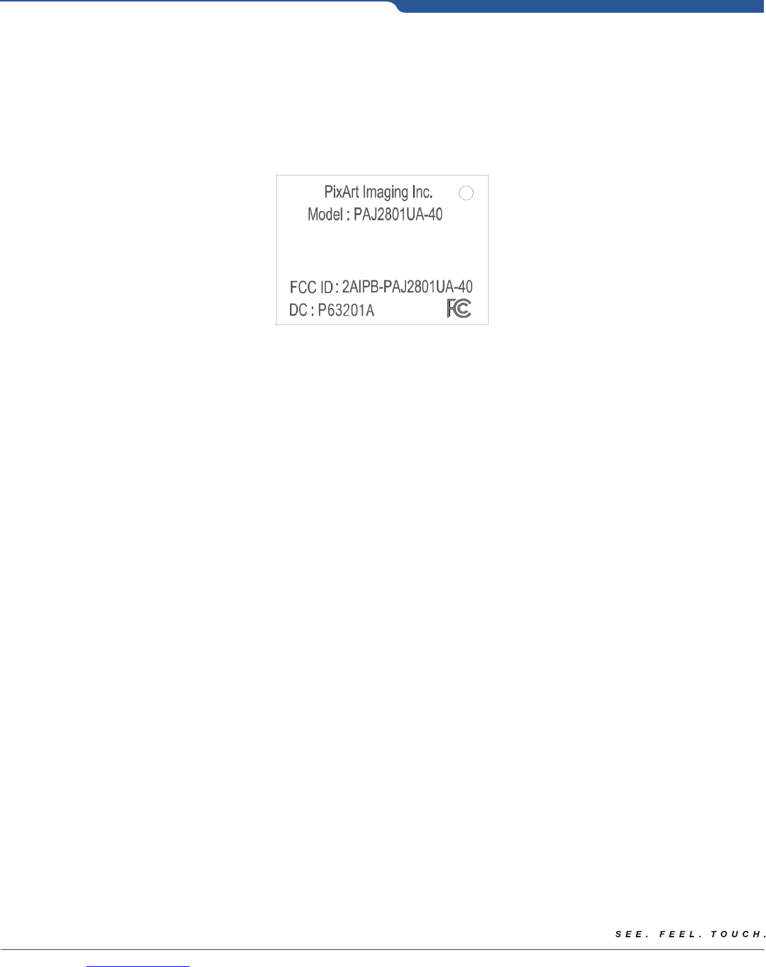
7.1 FCC
This device complies with Part 15 of the FCC Rules. Operation is subject to the following two conditions: (1) this device may
not cause harmful interference, and (2) this device must accept any interference received, including interference that may
cause undesired operation.
FCC ID: 2AIPB-PAJ2801UA-40
Figure 7. Label (Laser Marking)

17
PixArt Imaging Inc.
PixArt Imaging Inc. http://www.pixart.com
All rights reserved. Any portion in this paper shall not be reproduced, copied, or transformed to any other forms without permission.
PAJ2801UA-40 User’s Manual
Low Power Bluetooth 4.0 Module
Version 0.34 |29 Jul 2016
Document Revision History
Revision Number
Date
Description
0.1
26 Mar 2016
1st draft
0.2
16 Jun 2016
2nd draft
0.3
06 Jul 2016
1. Modify the PA no.
2. Modify the Figure 8. Recommended Module Footprint
0.31
06 Jul 2016
3. Add the chapter 8: End-Product Label
0.32
25 Jul 2016
1. Add the chapter 8: End-Product Label
2. Modify the Key parameters
0.33
25 July 2016
1. Add the Figure 14. Label (Laser Marking)
0.34
29 July 2016
1. Modify the Figure 14. Label (Laser Marking)