Pmc Sierra Pm25Lv010 Users Manual SPI Data Sheets
Pm25LV010 Pm25LV512-010
Pm25LV010 to the manual 3e67cf7b-3cbf-41ef-873d-2bd92dca3466
2015-02-06
: Pmc-Sierra Pmc-Sierra-Pm25Lv010-Users-Manual-519572 pmc-sierra-pm25lv010-users-manual-519572 pmc-sierra pdf
Open the PDF directly: View PDF ![]() .
.
Page Count: 24

512 Kbit / 1 Mbit 3.0 Volt-only, Serial Flash Memory
With 25 MHz SPI Bus Interface
PMC
FEATURES
Single Power Supply Operation
- Low voltage range: 2.7 V - 3.6 V
• Memory Organization
- Pm25LV512: 64K x 8 (512 Kbit)
- Pm25LV010: 128K x 8 (1 Mbit)
Cost Effective Sector/Block Architecture
- Uniform 4 Kbyte sectors
- Uniform 32 Kbyte blocks (8 sectors per block)
- Two blocks with 32 Kbytes each (512 Kbit)
- Four blocks with 32 Kbytes each (1 Mbit)
- 128 pages per block
Serial Peripheral Interface (SPI) Compatible
- Supports SPI Modes 0 (0,0) and 3 (1,1)
High Performance Read
- 25 MHz clock rate (maximum)
Page Mode for Program Operations
- 256 bytes per page
Block Write Protection
- The Block Protect (BP1, BP0) bits allow part or entire
of the memory to be configured as read-only.
Hardware Data Protection
- Write Protect (WP#) pin will inhibit write operations
to the status register
• Page Program (up to 256 Bytes)
- Typical 2 ms per page program time
• Sector, Block and Chip Erase
- Typical 40 ms sector/block/chip erase time
Single Cycle Reprogramming for Status Register
- Build-in erase before programming
High Product Endurance
- Guarantee 100,000 program/erase cycles per single
sector (preliminary)
- Minimum 20 years data retention
Industrial Standard Pin-out and Package
- 8-pin JEDEC SOIC
- 8-contact WSON
- Optional lead-free (Pb-free) packages
GENERAL DESCRIPTION
The Pm25LV512/010 are 512 Kbit/1 Mbits 3.0 Volt-only serial Flash memories. These devices are designed to use
a single low voltage, range from 2.7 Volt to 3.6 Volt, power supply to perform read, erase and program operations.
The devices can be programmed in standard EPROM programmers as well.
The device is optimized for use in many commercial applications where low-power and low-voltage operation are
essential. The Pm25LV512/010 is enabled through the Chip Enable pin (CE#) and accessed via a 3-wire interface
consisting of Serial Data Input (Sl), Serial Data Output (SO), and Serial Clock (SCK). All write cycles are com-
pletely self-timed.
Block Write protection for top 1/4, top 1/2 or the entire memory array (1M) or entire memory array (512K) is enabled
by programming the status register. Separate write enable and write disable instructions are provided for additional
data protection. Hardware data protection is provided via the WP pin to protect against inadvertent write attempts
to the status register. The HOLD pin may be used to suspend any serial communication without resetting the serial
sequence.
Programmable Microelectronics Corp. 1Issue Date: February, 2004, Rev: 1.4
Pm25LV512 / Pm25LV010
The Pm25LV512/010 are manufactured on PMC’s advanced nonvolatile CMOS technology, P-FLASH™. The de-
vices are offered in 8-pin JEDEC SOIC and 8-contact WSON packages with operation frequency up to 25 MHz.
2
Programmable Microelectronics Corp. Issue Date: February, 2004, Rev: 1.4
PMC Pm25LV512/010
PIN DESCRIPTIONS
LOBMYSEPYTNOITPIRCSED
#ECTUPNI
rofseirtiucriclanretnis'ecivedehtsetavitcawolseog#EC:elbanEpihC otnisehctiwsdnaecivedehtstcelesedhgihseog#EC.noitarepoecived tonsiecivedehtnehW.noitpmusnocrewopehtecuderotedomybdnats ehtdna,)lS(niptupnilairesehtaivdetpeccaebtonlliwatad,detceles .etatsecnadepmihgihaniniamerlliw)OS(niptuptuolaires
KCSTUPNIkcolCataDlaireS
ISTUPNItupnIataDlaireS
OSTUPTUOtuptuOataDlaireS
DNGdnuorG
ccVylppuSrewoPeciveD
#PWTUPNI lla,"1"sitibNEPWdnawolotthguorbnip#PWehtnehW:tcetorPetirW .detibihnieraretsigersutatsehtotsnoitarepoetirw
#DLOHTUPNI tuohtiwecivedretsamehthtiwnoitacinummoclairesesuaP:dloH .ecneuqeslairesehtgnitteser
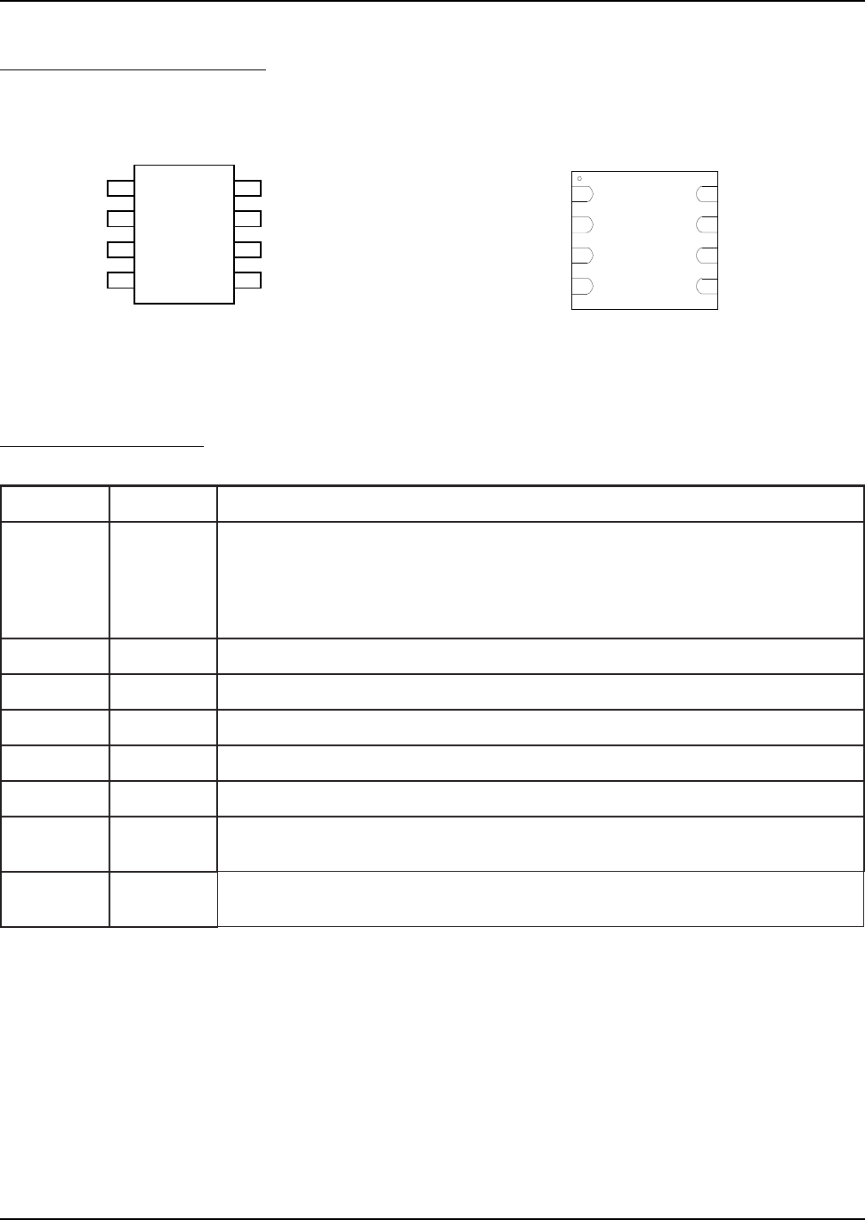
CONNECTION DIAGRAMS
8-Pin SOIC
5
6
7
81
2
3
4
Vcc
HOLD#
SCK
SI
SO
GND
WP#
CE#
8-Contact WSON
5
6
7
8
1
2
3
4
Vcc
HOLD#
SCK
SI
SO
GND
WP#
CE#
Top View
3
Programmable Microelectronics Corp. Issue Date: February, 2004, Rev: 1.4
PMC Pm25LV512/010
PRODUCT ORDERING INFORMATION
Pm25LVxxx -25 S C E
Temperature Range
C = Commercial (0°C to +85°C)
Package Type
S = 8-pin SOIC (8S)
Q = 8-contact WSON (8Q)
Operating Speed
25 MHz
PMC Device Number
Pm25LV512 (512 Kbit)
Pm25LV010 (1 Mbit)
Environmental Attribute
E = Lead-free (Pb-free) Package
Blank = Standard Package
Part Number Operating Frequency (MHz) Package Temperature Range
Pm25LV512-25SCE
Pm25LV512-25SC
Pm25LV512-25QCE 8Q
Pm25LV010-25SCE
Pm25LV010-25SC
Pm25LV010-25QCE 8Q
Commercial
(0oC to + 85oC)
8S
8S
25
25
4
Programmable Microelectronics Corp. Issue Date: February, 2004, Rev: 1.4
PMC Pm25LV512/010
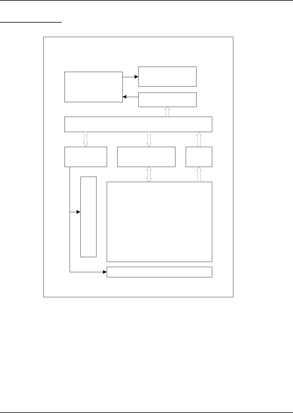
BLOCK DIAGRAM
High Voltage
Generator
Control Logic
Serial /Parallel convert Logic
Address Latch
& Counter
2KBit Page Buffer Status
Register
Memor
y
Arra
y
Y-DECODER
X-DECODER
Instruction Decoder
SPI Chip Block Dia
g
ram
5
Programmable Microelectronics Corp. Issue Date: February, 2004, Rev: 1.4
PMC Pm25LV512/010
Pm25LV512/010 can be driven by a microcontroller on the SPI bus as shown in Figure 1. The serial communication
term definitions are in the following section.
MASTER: The device that generates the serial clock.
SLAVE: Because the Serial Clock pin (SCK) is always an input, the Pm25LV512/010 always operates as a slave.
TRANSMITTER/RECEIVER: The Pm25LV512/010 has separate pins designated for data transmission (SO) and
reception (Sl).
MSB: The Most Significant Bit (MSB) is the first bit transmitted and received.
SERIAL OP-CODE: After the device is selected with CE# going low, the first byte will be received. This byte
contains the op-code that defines the operations to be performed.
INVALID OP-CODE: If an invalid op-code is received, no data will be shifted into the Pm25LV512/010, and the serial
output pin (SO) will remain in a high impedance state until the falling edge of CE# is detected again. This will
reinitialize the serial communication.
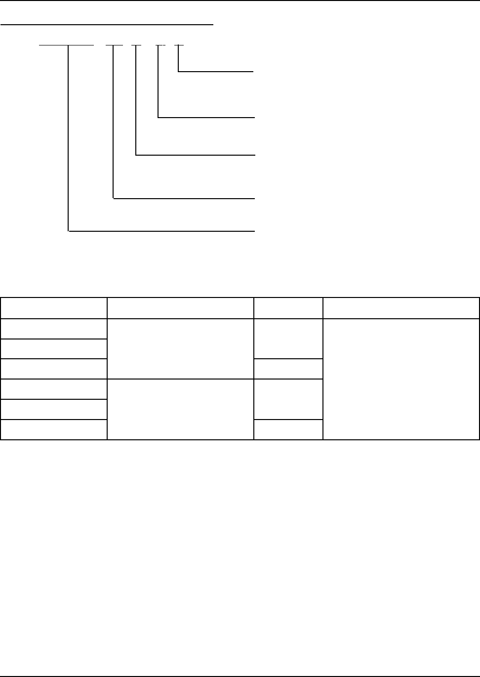
SERIAL INTERFACE DESCRIPTION
SPI Interface with
(0, 0) or (1, 1)
SDO
SDI
SCK
SCK SO SI
Bus Master
CS3 CS2 CS1
CE# WP# HOLD# HOLD# HOLD#
SPI Memory
Device SPI Memory
Device SPI Memory
Device
Note: 1. The Write Protect (WP#) and Hold (HOLD#) si
g
nals should be driven, Hi
g
h or Low as appropriate.
SCK SO SI SCK SO SI
CE# WP# CE# WP#
Figure 1. Bus Master and SPI Memory Devices
6
Programmable Microelectronics Corp. Issue Date: February, 2004, Rev: 1.4
PMC Pm25LV512/010
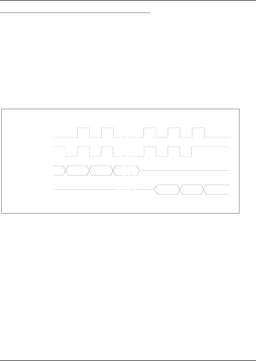
SPI MODES
These devices can be driven by microcontroller with its
SPI peripheral running in either of the two following modes:
Mode 0 = (0, 0)
Mode 3 = (1, 1)
For these two modes, input data is latched in on the
rising edge of Serial Clock (SCK), and output data is
available from the falling edge of Serial Clock (SCK).
The difference between the two modes, as shown in
Figure 2, is the clock polarity when the bus master is in
Stand-by mode and not transfering data:
- Clock remains at 0 (SCK = 0) for Mode 0 (0, 0)
- Clock remains at 1 (SCK = 1) for Mode 3 (1, 1)
Figure 2. SPI Modes
SCK
SCK
SI
SO
Mode 0 (0 0)
Mode 3 (1 1)
SERIAL INTERFACE DESCRIPTION (CONTINUED)
7
Programmable Microelectronics Corp. Issue Date: February, 2004, Rev: 1.4
PMC Pm25LV512/010
emaNnoitcurtsnItamroFnoitcurtsnIedoCxeHnoitarepO
NERW01100000h60hctaLelbanEetirWteS
IDRW00100000h40hctaLelbanEetirWteseR
RSDR10100000h50retsigersutatSdaeR
RSRW10000000h10retsigeRsutatSetirW
DAER11000000h30yrarrAyromeMmorfataDdaeR
DAER_TSAF11010000hB0deepSrehgiHtayromeMmorfataDdaeR
GORP_GP01000000h20yarrAyromeMotnIataDmargorP
ESARE_ROTCES11101011h7DyarrAyromeMnirotceSenOesarE
ESARE_KCOLB00011011h8DyarrAyromeMnikcolBenOesarE
ESARE_PIHC11100011h7CyarrAyromeMeritnEesarE
DIDR11010101hBADItcudorPdnarerutcafunaMdaeR
Table 1. Instruction Set for the Pm25LV512/010
DEVICE OPERATION
The Pm25LV512/010 is designed to interface directly with the synchronous serial peripheral interface (SPI) of the
6800 type series of microcontrollers.
The Pm25LV512/010 utilizes an 8-bit instruction register. The list of instructions and their operation codes are
contained in Table 1. All instructions, addresses, and data are transferred with the MSB first and start with a high-
to-low transition.
Write is defined as program and/or erase in this specification. The following commands, PAGE PROGRAM,
SECTOR ERASE, BLOCK ERASE, CHIP ERASE, and WRSR are write instructions for Pm25LV512/010.
noitacifitnedItcudorPataD
DIrerutcafunaMhD9
:DIeciveD
215VL52mPhB7
010VL52mPhC7
Table 2. Product Identification
READ PRODUCT ID (RDID): The RDID instruction allows the user to read the manufacturer and product ID of the
device. The instruction code is followed by three dummy bytes, each bit being latched-in on Serial Data Input (SI)
during the rising edge of Serial Clock (SCK). Then the first manufacturer ID (9Dh) is shifted out on Serial Data
Output (SO), followed by the device ID (7Bh = Pm25LV512; 7Ch = Pm25LV010) and the second manufacturer ID
(7Fh), each bit been shifted out during the falling edge of Serial Clock (SCK).
8
Programmable Microelectronics Corp. Issue Date: February, 2004, Rev: 1.4
PMC Pm25LV512/010
tiBnoitinifeD
)YDR(0tiB .YDAERsiecivedehtsetacidni0=0tiB siecivedehtdnassergorpnisielcycetirwehtsetacidni1=0tiB .YSUB
)NEW(1tiB .DELBANEETIRWtonsiecivedehtsetacidni0=1tiB .DELBANEETIRWsiecivedehtsetacidni1=1tiB
)0PB(2tiB.5elbaTeeS
)1PB(3tiB.5elbaTeeS
.elcycetirwlanretninanitonsiecivednehws0era6-4stiB
)NEPW(7tiB .)#PW(niptcetorPetirWfonoitcnufehtskcolb0=NEPW .)#PW(niptcetorPetirWehtsetavitca1=NEPW .sliatedrof6elbaTeeS
.elcycetirwlanretninagniruds1era7-0stiB
Table 4. Read Status Register Bit Definition
WRITE STATUS REGISTER (WRSR): The WRSR instruction allows the user to select one of four levels of protec-
tion for the Pm25LV010. The Pm25LV010 is divided into four blocks where the top quarter (1/4), top half (1/2), or all
of the memory blocks can be protected (locked out) from write. The Pm25LV512 is divided into 2 blocks where all
of the memory blocks can be protected (locked out) from write. Any of the locked-out blocks will therefore be READ
only. The locked-out block and the corresponding status register control bits are shown in Table 5.
The three bits, BP0, BP1, and WPEN, are nonvolatile cells that have the same properties and functions as the
regular memory cells (e.g., WREN, RDSR).
WRITE ENABLE (WREN): The device will power up in the write disable state when Vcc is applied. All write
instructions must therefore be preceded by the WREN instruction.
WRITE DISABLE (WRDI): To protect the device against inadvertent writes, the WRDI instruction disables all write
commands. The WRDI instruction is independent of the status of the WP# pin.
READ STATUS REGISTER (RDSR): The RDSR instruction provides access to the status register. The READY/
BUSY and write enable status of the device can be determined by the RDSR instruction. Similarly, the Block Write
Protection bits indicate the extent of protection employed. These bits are set by using the WRSR instruction.
During internal write cycles, all other commands will be ignored except the RDSR instruction.
7tiB6tiB5tiB4tiB3tiB2tiB1tiB0tiB
NEPW XXX 1PB0PBNEWYDR
Table 3. Status Register Format

9
Programmable Microelectronics Corp. Issue Date: February, 2004, Rev: 1.4
PMC Pm25LV512/010
NEPWPWNEWskcolBdetcetorPskcolBdetcetorpnUretsigeRsutatS
0X 0 detcetorPdetcetorPdetcetorP
0X 1 detcetorPelbatirWelbatirW
1woL0 detcetorPdetcetorPdetcetorP
1woL1 detcetorPelbatirWdetcetorP
XhgiH0 detcetorPdetcetorPdetcetorP
XhgiH1 detcetorPelbatirWelbatirW
Table 6. WPEN Operation
The WRSR instruction also allows the user to enable or disable the Write Protect (WP#) pin through the use of the
Write Protect Enable (WPEN) bit. Hardware write protection is enabled when the WP# pin is low and the WPEN bit
is "1". Hardware write protection is disabled when either the WP# pin is high or the WPEN bit is "0." When the
device is hardware write protected, writes to the Status Register, including the Block Protect bits and the WPEN
bit, and the locked-out blocks in the memory array are disabled. Write is only allowed to blocks of the memory
which are not locked out. The WRSR instruction is self-timed to automatically erase and program BP0, BP1, and
WPEN bits. In order to write the status register, the device must first be write enabled via the WREN instruction.
Then, the instruction and data for the three bits are entered. During the internal write cycle, all instructions will be
ignored except RDSR instructions. The Pm25LV512/010 will automatically return to write disable state at the
completion of the WRSR cycle.
Note: When the WPEN bit is hardware write protected, it cannot be changed back to "0", as long as the WP# pin
is held low.
leveL
stiBretsigeRsutatS215VL52mP010VL52mP
1PB0PB sesserddAyarrA tuOdekcoL tuo-dekcoL )s(kcolB sesserddAyarrA tuOdekcoL tuo-dekcoL )s(kcolB
000
enoNenoN
enoNenoN
)4/1(101 FFFF10-0008104kcolB
)2/1(210 FFFF10-0000104,3kcolB
)llA(311 FFFF00-000000 skcolBllA )2-1( FFFF10-000000 skcolBllA )4-1(
Table 5. Block Write Protect Bits

10
Programmable Microelectronics Corp. Issue Date: February, 2004, Rev: 1.4
PMC Pm25LV512/010
READ: Reading the Pm25LV512/010 via the SO (Serial Output) pin requires the following sequence. After the CE#
line is pulled low to select a device, the READ instruction is transmitted via the Sl line followed by the byte address
to be read (Refer to Table 7). Upon completion, any data on the Sl line will be ignored. The data (D7-D0) at
the specified address is then shifted out onto the SO line. If only one byte is to be read, the CE# line should be
driven high after the data comes out. The READ instruction can be continued since the byte address is automati-
cally incremented and data will continue to be shifted out. For the Pm25LV512/010, when the highest address is
reached, the address counter will roll over to the lowest address allowing the entire memory to be read in one
continuous READ instruction.
FAST_READ: The device is first selected by driving CE# low. The FAST READ instruction is followed by a 3-byte
address (A23-A0) and a dummy byte, each bit being latched-in during the rising edge of SCK (Serial Clock). Then
the memory contents, at that address, is shifted out on SO (Serial Output), each bit being shifted out, at a
maximum frequency fFR, during the falling edge of SCK (Serial Clock).
The first byte addressed can be at any location. The address is automatically incremented to the next higher
address after each byte of data is shifted out. When the highest address is reached, the address counter will roll
over to the lowest address allowing the entire memory to be read with a single FAST READ instruction. The FAST
READ instruction is terminated by driving CE# high.
PAGE PROGRAM (PG_PROG): In order to program the Pm25LV512/010, two separate instructions must be
executed. First, the device must be write enabled via the WREN instruction. Then the PAGE PROGRAM instruc-
tion can be executed. Also, the address of the memory location(s) to be programmed must be outside the pro-
tected address field location selected by the Block Write Protection Level. During an internal self-timed program-
ming cycle, all commands will be ignored except the RDSR instruction.
The PAGE PROGRAM instruction requires the following sequence. After the CE# line is pulled low to select the
device, the PAGE PROGRAM instruction is transmitted via the Sl line followed by the address and the data (D7-D0)
to be programmed (Refer to Table 7). Programming will start after the CE# pin is brought high. The low-to-high
transition of the CE# pin must occur during the SCK low time immediately after clocking in the D0 (LSB) data bit.
The READY/BUSY status of the device can be determined by initiating a RDSR instruction. If Bit 0 = 1, the program
cycle is still in progress. If Bit 0=0, the program cycle has ended. Only the RDSR instruction is enabled during the
program cycle. A single PROGRAM instruction programs 1 to 256 consecutive bytes within a page if it is not write
protected. The starting byte could be anywhere within the page. When the end of the page is reached, the address
will wrap around to the beginning of the same page. If the data to be programmed are less than a full page, the data
of all other bytes on the same page will remain unchanged. If more than 256 bytes of data are provided, the address
counter will roll over on the same page and the previous data provided will be replaced. The same byte cannot be
reprogrammed without erasing the whole sector/block first. The Pm25LV512/010 will automatically return to the
write disable state at the completion of the PROGRAM cycle.
Note: If the device is not write enabled (WREN) the device will ignore the Write instruction and will return to the
standby state, when CE# is brought high. A new CE# falling edge is required to re-initiate the serial
communication.
sserddA215VL52mP010VL52mP
A
N
A
51
A-
0
A
61
A-
0
stiBeraCt'noDA
32
A-
61
A
32
A-
71
Table 7. Address Key

11
Programmable Microelectronics Corp. Issue Date: February, 2004, Rev: 1.4
PMC Pm25LV512/010
sserddAkcolBkcolB215VL52mPkcolB010VL52mP
FFF700ot0000001kcolB1kcolB
FFFF00ot0008002kcolB2kcolB
FFF710ot000010A/N3kcolB
FFFF10ot000810A/N4kcolB
Table 8. Block Addresses
SECTOR_ERASE, BLOCK_ERASE: Before a byte can be reprogrammed, the sector/block which contains the
byte must be erased. In order to erase the Pm25LV512/010, two separate instructions must be executed. First, the
device must be write enabled via the WREN instruction. Then the SECTOR ERASE or BLOCK ERASE instruction
can be executed.
The BLOCK ERASE instruction erases every byte in the selected block if the block is not locked out. Block
address is automatically determined if any address within the block is selected. The BLOCK ERASE instruction
is internally controlled; it will automatically be timed to completion. During this time, all commands will be ignored,
except RDSR instruction. The Pm25LV512/010 will automatically return to the write disable state at the completion
of the BLOCK ERASE cycle.
CHIP_ERASE: As an alternative to the SECTOR and BLOCK ERASE, the CHIP ERASE instruction will erase
every byte in all blocks that are not locked out. First, the device must be write enabled via the WREN instruction.
Then the CHIP ERASE instruction can be executed. The CHIP ERASE instruction is internally controlled; it will
automatically be timed to completion. The CHIP ERASE cycle time maximum is 100 miliseconds. During the
internal erase cycle, all instructions will be ignored except RDSR. The Pm25LV512/010 will automatically return to
the write disable state at the completion of the CHIP ERASE.
HOLD: The HOLD# pin is used in conjunction with the CE# pin to select the Pm25LV512/010. When the device is
selected and a serial sequence is underway, HOLD# pin can be used to pause the serial communication with the
master device without resetting the serial sequence. To pause, the HOLD# pin must be brought low while the SCK
pin is low. To resume serial communication, the HOLD# pin is brought high while the SCK pin is low (SCK may still
toggle during HOLD). Inputs to the Sl pin will be ignored while the SO pin is in the high impedance state.
HARDWARE WRITE PROTECT: The Pm25LV512/010 has a write lockout feature that can be activated by assert-
ing the write protect pin (WP#). When the lockout feature is activated, locked-out sectors will be READ only. The
write protect pin will allow normal read/write operations when held high. When the WP# is brought low and WPEN
bit is "1", all write operations to the status register are inhibited. WP# going low while CE# is still low will interrupt
a write to the status register. If the internal status register write cycle has already been initiated, WP# going low will
have no effect on any write operation to the status register. The WP# pin function is blocked when the WPEN bit in
the status register is "0". This will allow the user to install the Pm25LV512/010 in a system with the WP# pin tied
to ground and still be able to write to the status register. All WP# pin functions are enabled when the WPEN bit is
set to "1".
12
Programmable Microelectronics Corp. Issue Date: February, 2004, Rev: 1.4
PMC Pm25LV512/010
DC AND AC OPERATING RANGE
ABSOLUTE MAXIMUM RATINGS (1)
Notes:
1. Stresses under those listed in “Absolute Maximum Ratings” may cause permanent damage
to the device. This is a stress rating only. The functional operation of the device or any other
conditions under those indicated in the operational sections of this specification is not
implied. Exposure to absolute maximum rating condition for extended periods may affected
device reliability.
2. Maximum DC voltage on input or I/O pins are VCC + 0.5 V. During voltage transitioning
period, input or I/O pins may overshoot to VCC + 2.0 V for a period of time up to 20 ns.
Minimum DC voltage on input or I/O pins are -0.5 V. During voltage transitioning period,
input or I/O pins may undershoot GND to -2.0 V for a period of time up to 20 ns.
saiBrednUerutarepmeT 56-
o
521+otC
o
C
erutarepmeTegarotS 56-
o
521+otC
o
C
erutarepmeTgniredloSdaeLtnuoMecafruS egakcaPdradnatS042
o
sdnoceS3C
egakcaPeerf-daeL062
o
sdnoceS3C
sniPllAnodnuorGottcepseRhtiwegatloVtupnI
)2(
VotV5.0-
CC
V5.0+
dnuorGottcepseRhtiwegatloVtuptuOllA VotV5.0-
CC
V5.0+
V
CC )2(
V0.6+otV5.0-
rebmuNtraP 010/215VL52mP
erutarepmeTgnitarepO 0
o
58otC
o
C
ylppuSrewoPccV V6.3-V7.2
13
Programmable Microelectronics Corp. Issue Date: February, 2004, Rev: 1.4
PMC Pm25LV512/010
DC CHARACTERISTICS
Applicable over recommended operating range from:
TAC = 0°C to +85°C, VCC = +2.7 V to +3.6 V (unless otherwise noted).
Symbol Parameter Min Typ Max Units
ICC1 Vcc Active Read Current 10 15 mA
ICC2 Vcc Program/Erase Current 15 30 mA
ISB1 Vcc Standby Current CMO
S
0.1 5 µA
ISB2 Vcc Standby Current TTL 0.05 3 mA
ILI Input Leakage Current 1 µA
ILO Output Leakage Current 1 µA
VIL Input Low Voltage -0.5 0.8 V
VIH Input HIgh Voltage 0.7VCC VCC + 0.3 V
VOL Output Low Voltage IOL = 2.1 mA 0.45 V
VOH Output High Voltage IOH = -100 µAV
CC - 0.2 V
2.7V < VCC < 3.6V
VCC = 3.6V, CE# = VIH to VCC
VIN = 0V to VCC
VIN = 0V to VCC, TAC = 0oC to 85oC
Condition
VCC = 3.6V at 25 MHz, SO = Open
VCC = 3.6V at 25 MHz, SO = Open
VCC = 3.6V, CE# = VCC

14
Programmable Microelectronics Corp. Issue Date: February, 2004, Rev: 1.4
PMC Pm25LV512/010
lobmySretemaraPniMpyTxaMstinU
f
RF
rofycneuqerFkcolC DAER_TSAF 052zHM
f
R
snoitcurtsniDAERrofycneuqerFkcolC002zHM
t
IR
emiTesiRtupnI 02sn
t
IF
emiTllaFtupnI 02sn
t
HKC
emiThgiHKCS02sn
t
LKC
emiTwoLKCS02sn
t
HEC
emiThgiHEC52sn
t
SC
emiTputeSEC52sn
t
HC
emiTdloHEC52sn
t
SD
emiTputeSnIataD5sn
t
HD
emiTdloHniataD5sn
t
SH
emiTputeSdloH51sn
t
DH
emiTdloH51sn
t
V
dilaVtuptuO 51sn
t
HO
emiTdloHtuptuO0sn
t
ZL
ZwoLtuptuOotdloH 002sn
t
ZH
ZhgiHtuptuOotdloH 002sn
t
SID
emiTelbasiDtuptuO 001sn
t
CE
emiTesarEpihC/kcolB/retceS04001sm
t
pp
emiTmargorPegaP25sm
t
w
emitretsigeRsutatSetirW04001sm
AC CHARACTERISTICS
Applicable over recommended operating range from TA = 0°C to +85°C, VCC = +2.7 V to +3.6 V
CL = 1TTL Gate and 30 pF (unless otherwise noted).
15
Programmable Microelectronics Corp. Issue Date: February, 2004, Rev: 1.4
PMC Pm25LV512/010
AC CHARACTERISTICS (CONTINUED)
AC WAVEFORMS(1)
Note: 1. For SPI Mode 0 (0,0)
OUTPUT TEST LOAD INPUT TEST WAVEFORMS
AND MEASUREMENT LEVEL
VALID IN
CE#
V
IL
V
IH
SCK
V
IH
V
IH
V
OH
V
IL
V
IL
V
OL
SI
SO
t
CS
t
CKH
t
CKL
t
CEH
t
DH
t
DS
t
V
t
DIS
t
OH
HI-Z
HI-Z
t
CH
3.3 V
1.8 K
1.3 K
OUTPUT PIN
30 pF
3.0 V
0.0 V
1.5 V AC
Measurement
Level
Input
16
Programmable Microelectronics Corp. Issue Date: February, 2004, Rev: 1.4
PMC Pm25LV512/010
AC CHARACTERISTICS (CONTINUED)
t
HD
t
HD
t
HS
t
HS
t
HZ
t
LZ
CE#
SCK
HOLD#
SO
HOLD Timing
pyTxaMstinUsnoitidnoC
C
NI
46 FpV
NI
V0=
C
TUO
821FpV
TUO
V0=
PIN CAPACITANCE ( f = 1 MHz, T = 25°C )
Note: These parameters are characterized but not 100% tested.
17
Programmable Microelectronics Corp. Issue Date: February, 2004, Rev: 1.4
PMC Pm25LV512/010
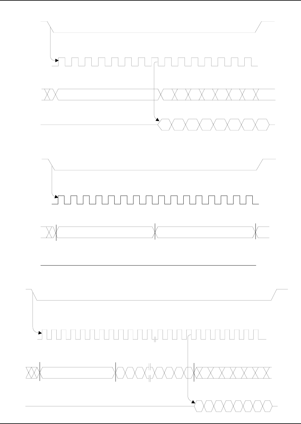
TIMING DIAGRAMS
SCK
SI
SO
INSTRUCTION = 0000 0110b
HI-Z
CE#
WREN Timing
WRDI Timing
CE#
SCK
SI
SO
INSTRUCTION = 0000 0100b
HI-Z
nnnnnnN
01 8 31 38 39 46 47 54
HIGH IMPEDANCE Manufacture ID1 Device ID Manufacture ID2
SCK
CE#
SI
SO
INSTRUCTION
97
1010 1011b
3 Dummy Bytes
RDID Timing
18
Programmable Microelectronics Corp. Issue Date: February, 2004, Rev: 1.4
PMC Pm25LV512/010
RDSR Timing
CE#
SCK
SI
012 3 5678910 11 12 13 14
4
INSTRUCTION = 0000 0101b
SO 765432 10
HIGH IMPEDANCE
DATA OUT
MSB
0 1 2 3 5 6 7 8 9 10 11 12 13 14415
7654 32
10
DATA IN
INSTRUCTION = 0000 0001b
HIGH IMPEDANCE
CE#
SCK
SI
SO
WRSR Timing
READ Timing
0 1 2 3 4 5 6 7 8 9 10 11 28 29 30 31 32 33 34 3635 37 38
...
23 22 21 3 2 1 0
76543210
3-BYTE ADDRESS
INSTRUCTION = 0000 0011b
HIGH IMPEDANCE
CE#
SCK
SI
SO
19
Programmable Microelectronics Corp. Issue Date: February, 2004, Rev: 1.4
PMC Pm25LV512/010
PAGE PROGRAM Timing
0 1 2 3 4 5 6 7 8 9 10 11 28 29 30 31 32 33 34
2075
2076
2077
2078
2079
076 532 21143023 22 21
1st BYTE DATA-IN 256th BYTE DATA-IN
3-BYTE ADDRESS
INSTRUCTION = 0000 0010b
HIGH IMPEDANCE
CE#
SCK
SI
SO
FAST READ Timing
0 1 2 3 4 5 6 7 8 9 10 11 28 29 30 31
...
23 22 21 3 2 1 0
3-BYTE ADDRESS
INSTRUCTION = 0000 1011b
HIGH IMPEDANCE
CE#
SCK
SI
SO
32 33 34 35 36 37 38 39 40 41 42 43 44 45 46 47
765 30
76543210
HIGH IMPEDANCE
CE#
SCK
SI
SO
4 1
76543210
2
DATA OUT 1 DATA OUT 2
DUMMY BYTE
20
Programmable Microelectronics Corp. Issue Date: February, 2004, Rev: 1.4
PMC Pm25LV512/010
BLOCK ERASE Timing
CHIP ERASE Timing
01 234 56789101128 29 30 31
0123212223
...
3-BYTE ADDRESS
INSTRUCTION = 1101 1000b
HIGH IMPEDANCE
CE#
SCK
SI
SO
01234567
HIGH IMPEDANCE
SCK
CE#
SI
SO
INSTRUCTION = 1100 0111b
0 1 2 3 4 5 6 7 8 9 10 11 28 29 30 31
0123212223
...
3-BYTE ADDRESS
INSTRUCTION = 1101 0111b
HIGH IMPEDANCE
CE#
SCK
SI
SO
SECTOR ERASE Timing
21
Programmable Microelectronics Corp. Issue Date: February, 2004, Rev: 1.4
PMC Pm25LV512/010
PROGRAM/ERASE PERFORMANCE
retemaraPtinUpyTxaMskrameR
emiTesarErotceSsm04001noitelpmocesareotdnammocesaregnitirwmorF
emiTesarEkcolBsm04001noitelpmocesareotdnammocesaregnitirwmorF
emiTesarEpihCsm04001noitelpmocesareotdnammocesaregnitirwmorF
emiTgnimmargorPegaPsm25 margorpotdnammocmargorpgnitirwmorF noitelpmoc
retemaraPniMpyTtinUdohteMtseT
ecnarudnE000,001
)2(
selcyC711AdradnatSCEDEJ
noitneteRataD02sraeY301AdradnatSCEDEJ
ledoMydoBnamuH-DSE000,2stloV411AdradnatSCEDEJ
ledoMenihcaM-DSE002stloV511AdradnatSCEDEJ
pU-hctaL I+001
1CC
Am87dradnatSCEDEJ
Note: These parameters are characterized and are not 100% tested.
Note: 1. These parameters are characterized and are not 100% tested.
2. Preliminary specification only and will be formalized after cycling qualification test.
RELIABILITY CHARACTERISTICS (1)
22
Programmable Microelectronics Corp. Issue Date: February, 2004, Rev: 1.4
PMC Pm25LV512/010
End View
5.00
4.80
Top View Side View
4.00
3.80
6.20
5.80 1.75
1.35
0.25
0.10
0.51
0.33
1.27 BSC
0.25
0.19
1.27
0.40
45º
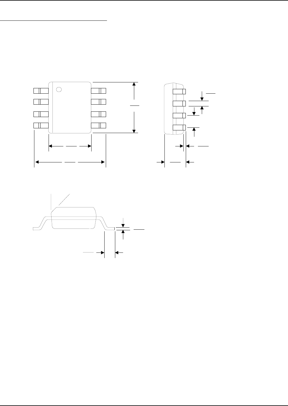
PACKAGE TYPE INFORMATION
8S
8-Pin JEDEC Small Outline Integrated Circuit (SOIC) Package (measure in millimeters)
23
Programmable Microelectronics Corp. Issue Date: February, 2004, Rev: 1.4
PMC Pm25LV512/010
PACKAGE TYPE INFORMATION (CONTINUED)
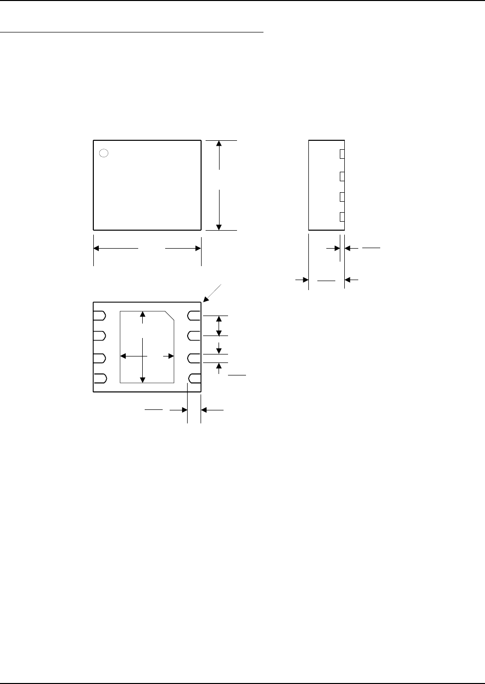
8Q
8-Contact Ulta-Thin Small Outline No-Lead (WSON) Package (measure in millimeters)
5.00
BSC
Top View Side View
0.48
0.35
6.00
BSC
0.80
0.70
0.25
0.19
1.27
BSC
Bottom View
Pin 1
0.75
0.50
4.00
3.40

24
Programmable Microelectronics Corp. Issue Date: February, 2004, Rev: 1.4
PMC Pm25LV512/010
REVISION HISTORY
etaD.oNnoisiveRsegnahCfonoitpircseD.oNegaP
2002,rebotcO0.1cepSyranimilerP,noitacilbupweNllA
2002,rebmeceD1.1esaeleRlamroFllA
3002,nuJ2.1noitpoegakcapNOSWdeddA32,3,2,1
3002,rebmeceD3.1
snoitpoegakcapeerf-daeLdeddA21,3,1
000,05morfselcycesare/margorpdeetnarugdedargpU )yranimilerp(000,001ot 12,1
noisnemidegakcapdewarderdnadetadpU32,22
4002,yraurbeF4.1egnarerutarepmetnoitarepoevorpmIllA
