Powertech Co EM3585 Zigbee Module User Manual EM3585
Powertech Industrial Co Ltd Zigbee Module EM3585
UserManual.wiki
>
Powertech Co
>
EM3585 User Manual
User Manual-Rev.02(151223)
Navigation menu
Upload a User Manual
Namespaces
Wiki Guide
HTML
PDF
Info
Views
User Manual
Discussion / Help
Navigation
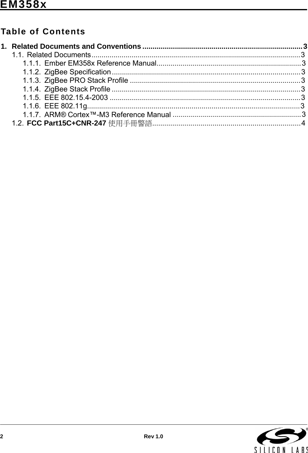
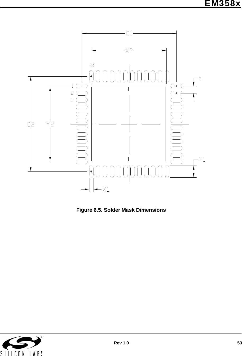
![EM358xRev 1.0 7Table 6.1. EM358x Pin Descriptions Pin # Signal Direction Description 1 VDD_24MHZ Power 1.8 V high-frequency oscillator supply 2 VDD_VCO Power 1.8 V VCO supply 3 RF_P I/O Differential (with RF_N) receiver input/transmitter output 4 RF_N I/O Differential (with RF_P) receiver input/transmitter output 5 VDD_RF Power 1.8 V RF supply (LNA and PA) 6 RF_TX_ALT_P O Differential (with RF_TX_ALT_N) transmitter output (optional) 7 RF_TX_ALT_N O Differential (with RF_TX_ALT_P) transmitter output (optional) 8 VDD_IF Power 1.8 V IF supply (mixers and filters) 9 NC Do not connect 10 VDD_PADSA Power Analog pad supply (1.8 V) 11 PC5 I/O Digital I/O TX_ACTIVE O Logic-level control for external RX/TX switch. The EM358x baseband con- trols TX_ACTIVE and drives it high (VDD_PADS) when in TX mode. Select alternate output function with GPIO_PCCFGH[7:4] 12 nRESET I Active low chip reset (internal pull-up) 13 PC6 I/O Digital I/O OSC32B I/O 32.768 kHz crystal oscillator Select analog function with GPIO_PCCFGH[11:8] nTX_ACTIVE O Inverted TX_ACTIVE signal (see PC5) Select alternate output function with GPIO_PCCFGH[11:8] 14 PC7 I/O Digital I/O OSC32A I/O 32.768 kHz crystal oscillator Select analog function with GPIO_PCCFGH[15:12] OSC32_EXT I Digital 32.768 kHz clock input source 15 VREG_OUT Power Regulator output (1.8 V while awake, 0 V during deep sleep) 16 VDD_PADS Power Pads supply (2.1–3.6 V) 17 VDD_CORE Power 1.25 V digital core supply decoupling Note: 1. IRQC and IRQD external interrupts can be mapped to any digital I/O pin using the GPIO_IRQCSEL and GPIO_IRQDSEL registers.](https://usermanual.wiki/Powertech-Co/EM3585/User-Guide-2853163-Page-7.png)
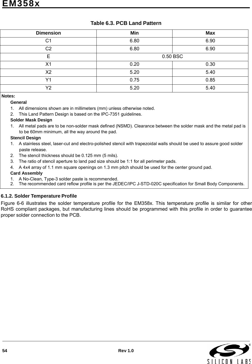
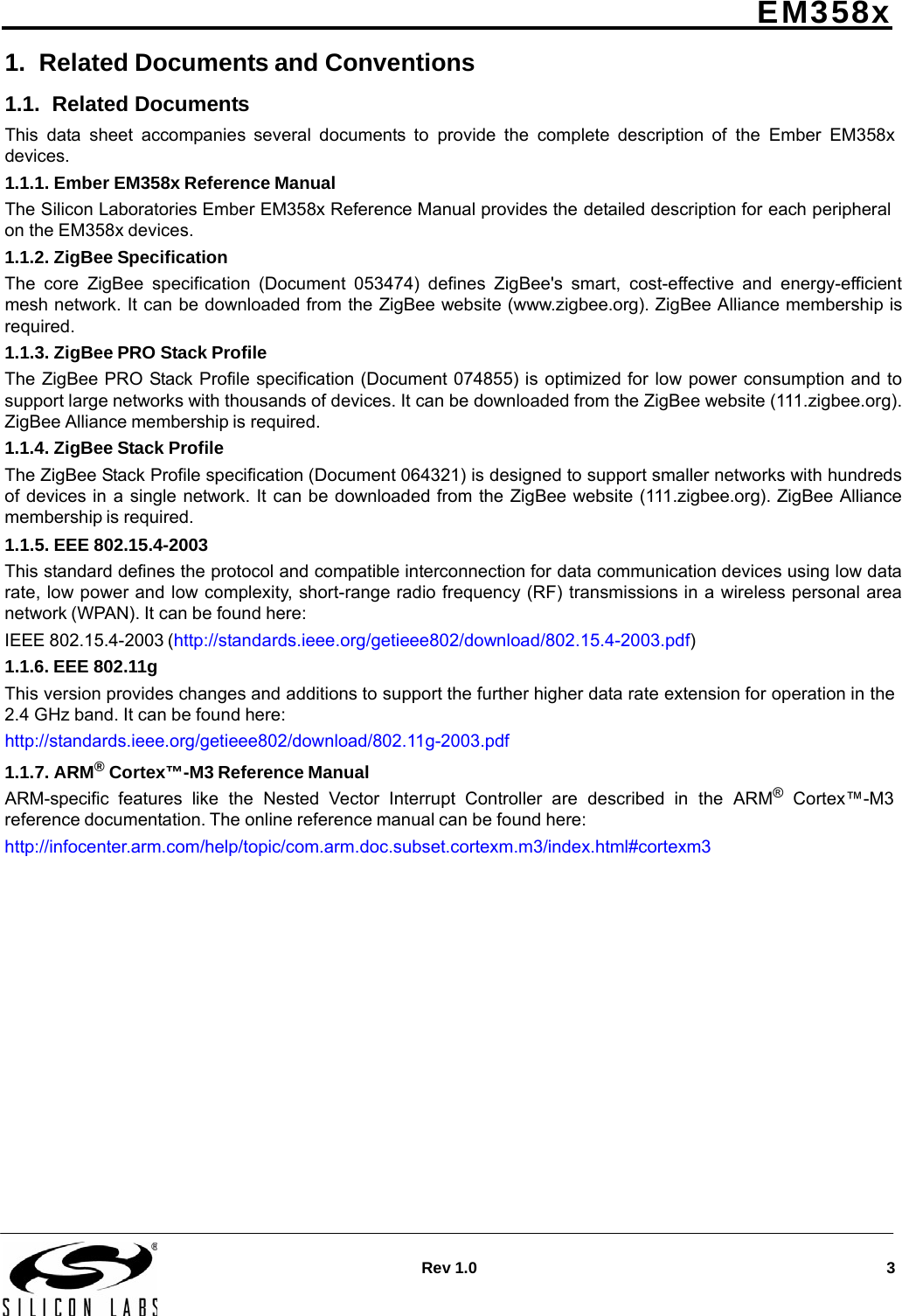
![8 Rev 1.0EM358x Table 6.1. EM358x Pin Descriptions (Continued)Pin # Signal Direction Description 18 PA7 I/O High current Digital I/O Disable REG_EN with GPIO_DBGCFG[4] TIM1C4 O Timer 1 Channel 4 output Enable timer output with TIM1_CCER Select alternate output function with GPIO_PACFGH[15:12] Disable REG_EN with GPIO_DBGCFG[4] TIM1C4 I Timer 1 Channel 4 input Cannot be remapped REG_EN O External regulator open drain output Enabled after reset 19 PB3 I/O Digital I/O TIM2C3 (see also Pin 22) O Timer 2 channel 3 output Enable remap with TIM2_OR[6] Enable timer output in TIM2_CCER Select alternate output function with GPIO_PBCFGL[15:12] TIM2C3 (see also Pin 22) I Timer 2 channel 3 input Enable remap with TIM2_OR[6] SC1nCTS I UART CTS handshake of Serial Controller 1 Enable with SC1_UARTCFG[5] Select UART with SC1_MODE SC1SCLK O SPI master clock of Serial Controller 1 Either disable timer output in TIM2_CCER, or disable remap with TIM2_OR[6] Enable master with SC1_SPICFG[4] Select SPI with SC1_MODE Select alternate output function with GPIO_PBCFGL[15:12] SC1SCLK I SPI slave clock of Serial Controller 1 Enable slave with SC1_SPICFG[4] Select SPI with SC1_MODE Note: 1. IRQC and IRQD external interrupts can be mapped to any digital I/O pin using the GPIO_IRQCSEL and GPIO_IRQDSEL registers.](https://usermanual.wiki/Powertech-Co/EM3585/User-Guide-2853163-Page-8.png)
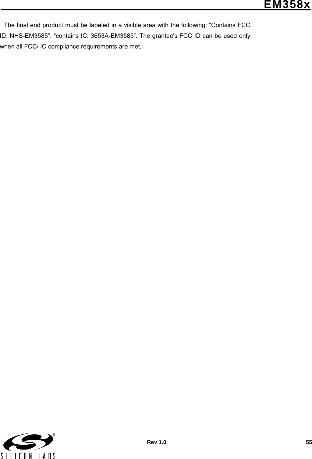
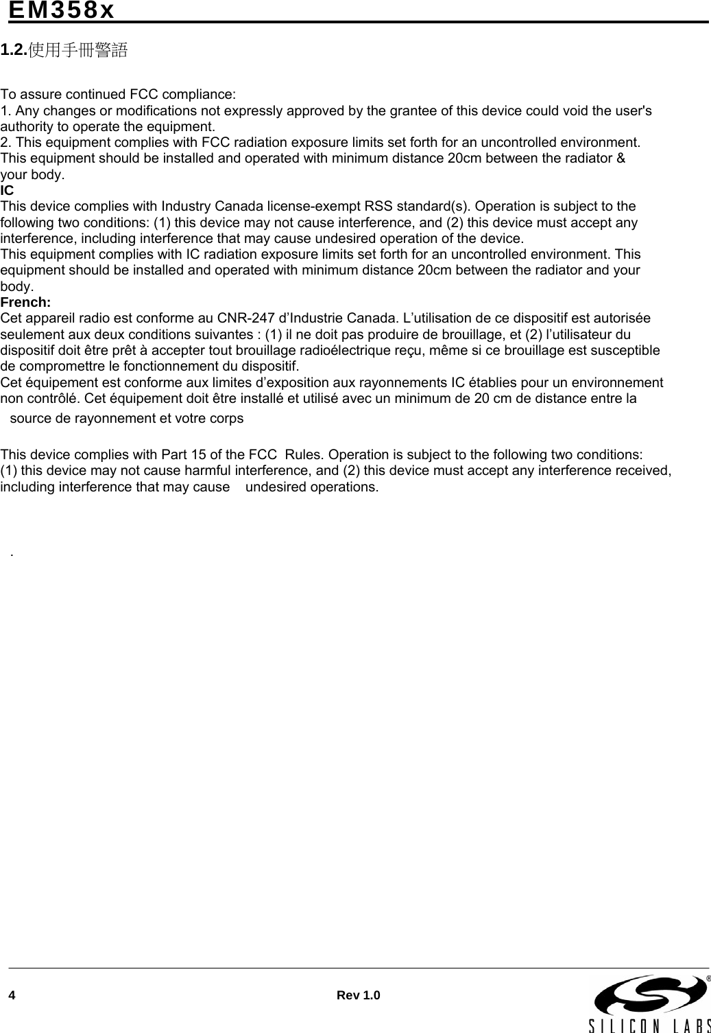
![Rev 1.0 9 EM358xTable 6.1. EM358x Pin Descriptions (Continued)Pin # Signal Direction Description 20 PB4 I/O Digital I/O TIM2C4 (see also Pin 24) O Timer 2 channel 4 output Enable remap with TIM2_OR[7] Enable timer output in TIM2_CCER Select alternate output function with GPIO_PBCFGH[3:0] TIM2C4 (see also Pin 24) I Timer 2 channel 4 input Enable remap with TIM2_OR[7] SC1nRTS O UART RTS handshake of Serial Controller 1 Either disable timer output in TIM2_CCER, or disable remap with TIM2_OR[7] Enable with SC1_UARTCFG[5] Select UART with SC1_MODE Select alternate output function with GPIO_PBCFGH[3:0] SC1nSSEL I SPI slave select of Serial Controller 1 Enable slave with SC1_SPICFG[4] Select SPI with SC1_MODE 21 PA0 I/O Digital I/O USBDM (where applicable) I/O USB D- signal Select analog function with GPIO_PACFGL[3:0] TIM2C1 (see also Pin 30) O Timer 2 channel 1 output Disable remap with TIM2_OR[4] Enable timer output in TIM2_CCER Select alternate output function with GPIO_PACFGL[3:0] TIM2C1 (see also Pin 30) I Timer 2 channel 1 input Disable remap with TIM2_OR[4] SC2MOSI O SPI master data out of Serial Controller 2 Either disable timer output in TIM2_CCER, or enable remap with TIM2_OR[4] Enable master with SC2_SPICFG[4] Select SPI with SC2_MODE Select alternate output function with GPIO_PACFGL[3:0] SC2MOSI I SPI slave data in of Serial Controller 2 Enable slave with SC2_SPICFG[4] Select SPI with SC2_MODE Note: 1. IRQC and IRQD external interrupts can be mapped to any digital I/O pin using the GPIO_IRQCSEL and GPIO_IRQDSEL registers.](https://usermanual.wiki/Powertech-Co/EM3585/User-Guide-2853163-Page-9.png)
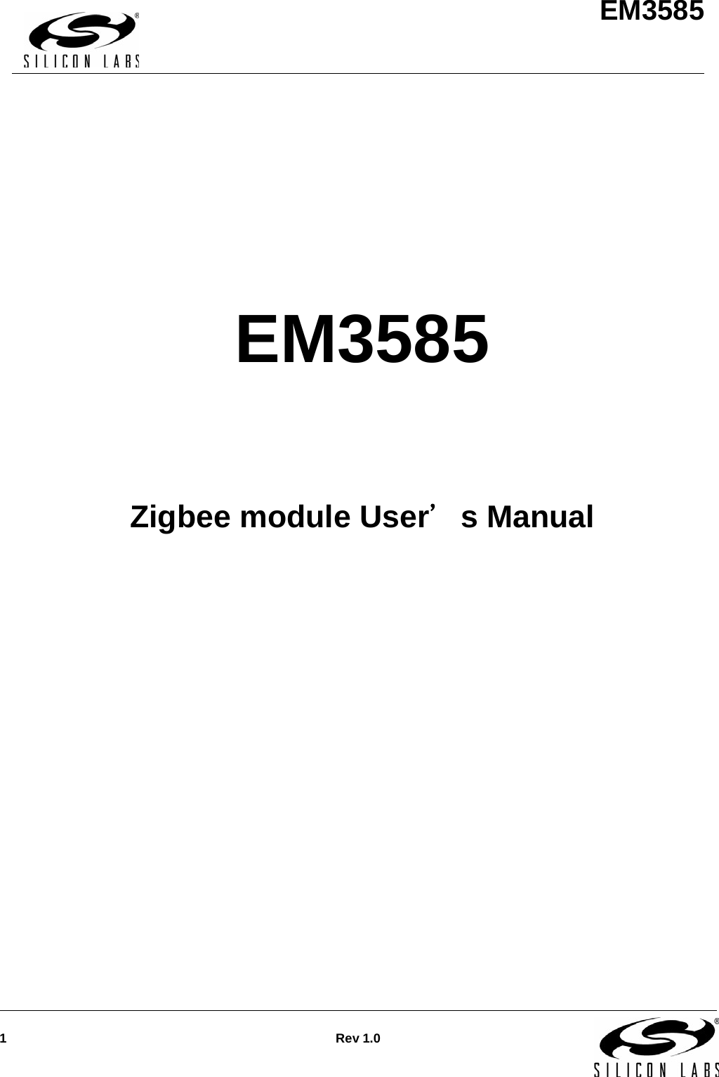
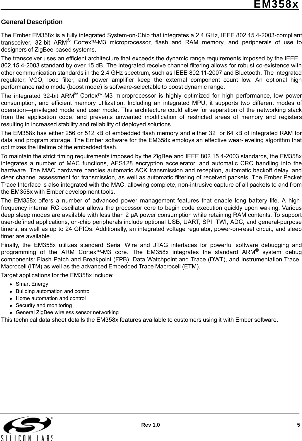
![EM358xTable 6.1. EM358x Pin Descriptions (Continued)Rev 1.0 41Pin # Signal Direction Description 22 PA1 I/O Digital I/O USBDP (where applicable) I/O USB D+ signal Select analog function with GPIO_PACFGL[7:4] TIM2C3 (see also Pin 19) O Timer 2 channel 3 output Disable remap with TIM2_OR[6] Enable timer output in TIM2_CCER Select alternate output function with GPIO_PACFGL[7:4] TIM2C3 (see also Pin 19) I Timer 2 channel 3 input Disable remap with TIM2_OR[6] SC2SDA I/O TWI data of Serial Controller 2 Either disable timer output in TIM2_CCER, or enable remap with TIM2_OR[6] Select TWI with SC2_MODE Select alternate open-drain output function with GPIO_PACFGL[7:4] SC2MISO O SPI slave data out of Serial Controller 2 Either disable timer output in TIM2_CCER, or enable remap with TIM2_OR[6] Enable slave with SC2_SPICFG[4] Select SPI with SC2_MODE Select alternate output function with GPIO_PACFGL[7:4] SC2MISO I SPI master data in of Serial Controller 2 Enable slave with SC2_SPICFG[4] Select SPI with SC2_MODE 23 VDD_PADS Power Pads supply (2.1–3.6 V) Note: 1. IRQC and IRQD external interrupts can be mapped to any digital I/O pin using the GPIO_IRQCSEL and GPIO_IRQDSEL registers.](https://usermanual.wiki/Powertech-Co/EM3585/User-Guide-2853163-Page-11.png)
![EM358x Table 6.1. EM358x Pin Descriptions (Continued)42 Rev 1.0Pin # Signal Direction Description 24 PA2 I/O Digital I/O TIM2C4 (see also Pin 20) O Timer 2 channel 4 output Disable remap with TIM2_OR[7] Enable timer output in TIM2_CCER Select alternate output function with GPIO_PACFGL[11:8] TIM2C4 (see also Pin 20) I Timer 2 channel 4 input Disable remap with TIM2_OR[7] SC2SCL I/O TWI clock of Serial Controller 2 Either disable timer output in TIM2_CCER, or enable remap with TIM2_OR[7] Select TWI with SC2_MODE Select alternate open-drain output function with GPIO_PACFGL[11:8] SC2SCLK O SPI master clock of Serial Controller 2 Either disable timer output in TIM2_CCER, or enable remap with TIM2_OR[7] Enable master with SC2_SPICFG[4] Select SPI with SC2_MODE Select alternate output function with GPIO_PACFGL[11:8] SC2SCLK I SPI slave clock of Serial Controller 2 Enable slave with SC2_SPICFG[4] Select SPI with SC2_MODE 25 PA3 I/O Digital I/O SC2nSSEL I SPI slave select of Serial Controller 2 Enable slave with SC2_SPICFG[4] Select SPI with SC2_MODE TIM2C2 (see also Pin 31) O Timer 2 channel 2 output Disable remap with TIM2_OR[5] Enable timer output in TIM2_CCER Select alternate output function with GPIO_PACFGL[15:12] TIM2C2 (see also Pin 31) I Timer 2 channel 2 input Disable remap with TIM2_OR[5] Note: 1. IRQC and IRQD external interrupts can be mapped to any digital I/O pin using the GPIO_IRQCSEL and GPIO_IRQDSEL registers.](https://usermanual.wiki/Powertech-Co/EM3585/User-Guide-2853163-Page-12.png)
![EM358xTable 6.1. EM358x Pin Descriptions (Continued)Rev 1.0 43Pin # Signal Direction Description 26 PA4 I/O Digital I/O ADC4 Analog ADC Input 4 Select analog function with GPIO_PACFGH[3:0] PTI_EN O Frame signal of Packet Trace Interface (PTI) Disable trace interface in ARM core Enable PTI in Ember software Select alternate output function with GPIO_PACFGH[3:0] TRACEDATA2 (see also Pin 36) O Synchronous CPU trace data bit 2 Select 4-wire synchronous trace interface in ARM core Enable trace interface in ARM core Select alternate output function with GPIO_PACFGH[3:0] 27 PA5 I/O Digital I/O ADC5 Analog ADC Input 5 Select analog function with GPIO_PACFGH[7:4] PTI_DATA O Data signal of Packet Trace Interface (PTI) Disable trace interface in ARM core Enable PTI in Ember software Select alternate output function with GPIO_PACFGH[7:4] nBOOTMODE I Activate FIB monitor instead of main program or bootloader when coming out of reset. Signal is active during and immediately after a reset on nRESET. Refer to section 7.5, Boot Configuration, in Chapter 7, GPIO, of the Ember EM358x Reference Manual for details. TRACEDATA3 (see also Pin 38) O Synchronous CPU trace data bit 3 Select 4-wire synchronous trace interface in ARM core Enable trace interface in ARM core Select alternate output function with GPIO_PACFGH[7:4] 28 VDD_PADS Power Pads supply (2.1–3.6 V) 29 PA6 I/O High cur- rent Digital I/O TIM1C3 O Timer 1 channel 3 output Enable timer output in TIM1_CCER Select alternate output function with GPIO_PACFGH[11:8] TIM1C3 I Timer 1 channel 3 input Cannot be remapped Note: 1. IRQC and IRQD external interrupts can be mapped to any digital I/O pin using the GPIO_IRQCSEL and GPIO_IRQDSEL registers.](https://usermanual.wiki/Powertech-Co/EM3585/User-Guide-2853163-Page-13.png)
![EM358x Table 6.1. EM358x Pin Descriptions (Continued)44 Rev 1.0Pin # Signal Direction Description 30 PB1 I/O Digital I/O SC1MISO O SPI slave data out of Serial Controller 1 Either disable timer output in TIM2_CCER, or disable remap with TIM2_OR[4] Select SPI with SC1_MODE Select slave with SC1_SPICFG Select alternate output function with GPIO_PBCFGL[7:4] SC1MOSI O SPI master data out of Serial Controller 1 Either disable timer output in TIM2_CCER, or disable remap with TIM2_OR[4] Select SPI with SC1_MODE Select master with SC1_SPICFG Select alternate output function with GPIO_PBCFGL[7:4] SC1SDA I/O TWI data of Serial Controller 1 Either disable timer output in TIM2_CCER, or disable remap with TIM2_OR[4] Select TWI with SC1_MODE Select alternate open-drain output function with GPIO_PBCFGL[7:4] SC1TXD O UART transmit data of Serial Controller 1 Either disable timer output in TIM2_CCER, or disable remap with TIM2_OR[4] Select UART with SC1_MODE Select alternate output function with GPIO_PBCFGL[7:4] TIM2C1 (see also Pin 21) O Timer 2 channel 1 output Enable remap with TIM2_OR[4] Enable timer output in TIM2_CCER Select alternate output function with GPIO_PACFGL[7:4] TIM2C1 (see also Pin 21) I Timer 2 channel 1 input Disable remap with TIM2_OR[4] Note: 1. IRQC and IRQD external interrupts can be mapped to any digital I/O pin using the GPIO_IRQCSEL and GPIO_IRQDSEL registers.](https://usermanual.wiki/Powertech-Co/EM3585/User-Guide-2853163-Page-14.png)
![EM358xTable 6.1. EM358x Pin Descriptions (Continued)Rev 1.0 45Pin # Signal Direction Description 31 PB2 I/O Digital I/O SC1MISO I SPI master data in of Serial Controller 1 Select SPI with SC1_MODE Select master with SC1_SPICFG SC1MOSI I SPI slave data in of Serial Controller 1 Select SPI with SC1_MODE Select slave with SC1_SPICFG SC1SCL I/O TWI clock of Serial Controller 1 Either disable timer output in TIM2_CCER,or disable remap with TIM2_OR[5] Select TWI with SC1_MODE Select alternate open-drain output function with GPIO_PBCFGL[11:8] SC1RXD I UART receive data of Serial Controller 1 Select UART with SC1_MODE TIM2C2 (see also Pin 25) O Timer 2 channel 2 output Enable remap with TIM2_OR[5] Enable timer output in TIM2_CCER Select alternate output function with GPIO_PBCFGL[11:8] TIM2C2 (see also Pin 25) I Timer 2 channel 2 input Enable remap with TIM2_OR[5] 32 SWCLK I/O Serial Wire clock input/output with debugger Selected when in Serial Wire mode (see JTMS description, Pin 35) JTCK I JTAG clock input from debugger Selected when in JTAG mode (default mode, see JTMS description, Pin 35) Internal pull-down is enabled Note: 1. IRQC and IRQD external interrupts can be mapped to any digital I/O pin using the GPIO_IRQCSEL and GPIO_IRQDSEL registers.](https://usermanual.wiki/Powertech-Co/EM3585/User-Guide-2853163-Page-15.png)
![EM358x Table 6.1. EM358x Pin Descriptions (Continued)46 Rev 1.0Pin # Signal Direction Description 33 PC2 I/O Digital I/O Enable with GPIO_DBGCFG[5] and GPIO_PCCFGH[1] clear JTDO O JTAG data out to debugger Selected when in JTAG mode (default mode, see JTMS description, Pin 35) SWO O Serial Wire Output asynchronous trace output to debugger Select asynchronous trace interface in ARM core Enable trace interface in ARM core Select alternate output function with GPIO_PCCFGL[11:8] Enable Serial Wire mode (see JTMS description, Pin 35) Internal pull-up is enabled TRACEDATA0 O Synchronous CPU trace data bit 3 Select 4-wire synchronous trace interface in ARM core Enable trace interface in ARM core Select alternate output function with GPIO_PACFGL[11:8] 34 PC3 I/O Digital I/O Either Enable with GPIO_DBGCFG[5],or enable Serial Wire mode (see JTMS description) JTDI I JTAG data in from debugger Selected when in JTAG mode (default mode, see JTMS description, Pin 35) Internal pull-up is enabled TRACECLK O Synchronous CPU trace clock Enable trace interface in ARM core Select alternate output function with GPIO_PCCFGL[15:12] 35 PC4 I/O Digital I/O Enable with GPIO_DBGCFG[5] JTMS I JTAG mode select from debugger Selected when in JTAG mode (default mode) JTAG mode is enabled after power-up or by forcing nRESET low Select Serial Wire mode using the ARM-defined protocol through a debug- ger Internal pull-up is enabled SWDIO I/O Serial Wire bidirectional data to/from debugger Enable Serial Wire mode (see JTMS description) Select Serial Wire mode using the ARM-defined protocol through a debug- ger Internal pull-up is enabled Note: 1. IRQC and IRQD external interrupts can be mapped to any digital I/O pin using the GPIO_IRQCSEL and GPIO_IRQDSEL registers.](https://usermanual.wiki/Powertech-Co/EM3585/User-Guide-2853163-Page-16.png)
![EM358xTable 6.1. EM358x Pin Descriptions (Continued)Rev 1.0 47Pin # Signal Direction Description 36 PB0 I/O Digital I/O VREF Analog O ADC reference output Enable analog function with GPIO_PBCFGL[3:0] VREF Analog I ADC reference input Enable analog function with GPIO_PBCFGL[3:0] Enable reference output with an Ember system function IRQA I External interrupt source A TRACEDATA2 (see also Pin 26) O Synchronous CPU trace data bit 2 Select 4-wire synchronous trace interface in ARM core Enable trace interface in ARM core Select alternate output function with GPIO_PBCFGL[3:0] TIM1CLK I Timer 1 external clock input TIM2MSK I Timer 2 external clock mask input 37 VDD_PADS Power Pads supply (2.1–3.6 V) 38 PC1 I/O Digital I/O ADC3 Analog ADC Input 3 Enable analog function with GPIO_PCCFGL[7:4] TRACEDATA3 (see also Pin 27) O Synchronous CPU trace data bit 3 Select 1-, 2- or 4-wire synchronous trace interface in ARM core Enable trace interface in ARM core Select alternate output function with GPIO_PCCFGL[7:4] 39 VDD_MEM Power 1.8 V supply (flash, RAM) 40 PC0 I/O High current Digital I/O Either enable with GPIO_DBGCFG[5],or enable Serial Wire mode (see JTMS description, Pin 35) and disable TRACEDATA1 JRST I JTAG reset input from debugger Selected when in JTAG mode (default mode, see JTMS description) and TRACEDATA1 is disabled Internal pull-up is enabled IRQD1 I Default external interrupt source D. TRACEDATA1 O Synchronous CPU trace data bit 1 Select 2- or 4-wire synchronous trace interface in ARM core Enable trace interface in ARM core Select alternate output function with GPIO_PCCFGL[3:0] Note: 1. IRQC and IRQD external interrupts can be mapped to any digital I/O pin using the GPIO_IRQCSEL and GPIO_IRQDSEL registers.](https://usermanual.wiki/Powertech-Co/EM3585/User-Guide-2853163-Page-17.png)
![EM358x Table 6.1. EM358x Pin Descriptions (Continued)48 Rev 1.0Pin # Signal Direction Description 41 PB7 I/O High current Digital I/O ADC2 Analog ADC Input 2 Enable analog function with GPIO_PBCFGH[15:12] IRQC1 I Default external interrupt source C. TIM1C2 O Timer 1 channel 2 output Enable timer output in TIM1_CCER Select alternate output function with GPIO_PBCFGH[15:12] TIM1C2 I Timer 1 channel 2 input Cannot be remapped 42 PB6 I/O High current Digital I/O ADC1 Analog ADC Input 1 Enable analog function with GPIO_PBCFGH[11:8] IRQB I External interrupt source B TIM1C1 O Timer 1 channel 1 output Enable timer output in TIM1_CCER Select alternate output function with GPIO_PBCFGH[11:8] TIM1C1 I Timer 1 channel 1 input Cannot be remapped 43 PB5 I/O Digital I/O ADC0 Analog ADC Input 0 Enable analog function with GPIO_PBCFGH[7:4] TIM2CLK I Timer 2 external clock input TIM1MSK I Timer 1 external clock mask input 44 VDD_CORE Power 1.25 V digital core supply decoupling 45 VDD_PRE Power 1.8 V prescaler supply 46 VDD_SYNTH Power 1.8 V synthesizer supply 47 OSCB I/O 24 MHz crystal oscillator or left open when using external clock input on OSCA Note: 1. IRQC and IRQD external interrupts can be mapped to any digital I/O pin using the GPIO_IRQCSEL and GPIO_IRQDSEL registers.](https://usermanual.wiki/Powertech-Co/EM3585/User-Guide-2853163-Page-18.png)