Powertech Co EM3585 Zigbee Module User Manual EM3585
Powertech Industrial Co Ltd Zigbee Module EM3585
User Manual-Rev.02(151223)

1 Rev 1.0
EM3585
EM3585
Zigbee module User’s Manual

EM358x
2 Rev 1.0
Table of
Content
s
1. Related Documents and Conventions ............................................................................... 3
1.1. Related Docume
nts
........................................................................................................
3
1.1.1. Ember EM358x Reference Manual
........................................................................
3
1.1.2. ZigBee Specification
..............................................................................................
3
1.1.3. ZigBee PRO Stack Profile
.....................................................................................
3
1.1.4. ZigBee Stack Profile
..............................................................................................
3
1.1.5. EEE 802.15.4-2003
...............................................................................................
3
1.1.6. EEE
802.11g..........................................................................................................
3
1.1.7. ARM® Cortex™-M3 Reference Manual
................................................................
3
1.2. FCC Part15C+CNR-247 使用手冊警語
..........................................................................
4

EM358x
Rev 1.0 3
1. Related Documents and Conventions
1.1. Related Documents
This data sheet accompanies several documents to provide the complete description of the Ember EM358x
devices.
1.1.1. Ember EM358x Reference Manual
The Silicon Laboratories Ember EM358x Reference Manual provides the detailed description for each peripheral
on the EM358x devices.
1.1.2. ZigBee Specification
The core ZigBee specification (Document 053474) defines ZigBee's smart, cost-effective and energy-efficient
mesh network. It can be downloaded from the ZigBee website (www.zigbee.org). ZigBee Alliance membership is
required.
1.1.3. ZigBee PRO Stack Profile
The ZigBee PRO Stack Profile specification (Document 074855) is optimized for low power consumption and to
support large networks with thousands of devices. It can be downloaded from the ZigBee website (111.zigbee.org).
ZigBee Alliance membership is required.
1.1.4. ZigBee Stack Profile
The ZigBee Stack Profile specification (Document 064321) is designed to support smaller networks with hundreds
of devices in a single network. It can be downloaded from the ZigBee website (111.zigbee.org). ZigBee Alliance
membership is required.
1.1.5. EEE 802.15.4-2003
This standard defines the protocol and compatible interconnection for data communication devices using low data
rate, low power and low complexity, short-range radio frequency (RF) transmissions in a wireless personal area
network (WPAN). It can be found here:
IEEE 802.15.4-2003 (http://standards.ieee.org/getieee802/download/802.15.4-2003.pdf)
1.1.6. EEE 802.11g
This version provides changes and additions to support the further higher data rate extension for operation in the
2.4 GHz band. It can be found here:
http://standards.ieee.org/getieee802/download/802.11g-2003.pdf
1.1.7. ARM® Cortex™-M3 Reference Manual
ARM-specific features like the Nested Vector Interrupt Controller are described in the ARM® Cortex™-M3
reference documentation. The online reference manual can be found here:
http://infocenter.arm.com/help/topic/com.arm.doc.subset.cortexm.m3/index.html#cortexm3

EM358x
4 Rev 1.0
1.2.使用手冊警語
To assure continued FCC compliance:
1. Any changes or modifications not expressly approved by the grantee of this device could void the user's
authority to operate the equipment.
2. This equipment complies with FCC radiation exposure limits set forth for an uncontrolled environment.
This equipment should be installed and operated with minimum distance 20cm between the radiator &
your body.
IC
This device complies with Industry Canada license-exempt RSS standard(s). Operation is subject to the
following two conditions: (1) this device may not cause interference, and (2) this device must accept any
interference, including interference that may cause undesired operation of the device.
This equipment complies with IC radiation exposure limits set forth for an uncontrolled environment. This
equipment should be installed and operated with minimum distance 20cm between the radiator and your
body.
French:
Cet appareil radio est conforme au CNR-247 d’Industrie Canada. L’utilisation de ce dispositif est autorisée
seulement aux deux conditions suivantes : (1) il ne doit pas produire de brouillage, et (2) l’utilisateur du
dispositif doit être prêt à accepter tout brouillage radioélectrique reçu, même si ce brouillage est susceptible
de compromettre le fonctionnement du dispositif.
Cet équipement est conforme aux limites d’exposition aux rayonnements IC établies pour un environnement
non contrôlé. Cet équipement doit être installé et utilisé avec un minimum de 20 cm de distance entre la
source de rayonnement et votre corps
This device complies with Part 15 of the FCC Rules. Operation is subject to the following two conditions:
(1) this device may not cause harmful interference, and (2) this device must accept any interference received,
including interference that may cause undesired operations.
.

EM358x
Rev 1.0 5
General Description
The Ember EM358x is a fully integrated System-on-Chip that integrates a 2.4 GHz, IEEE 802.15.4-2003-compliant
transceiver, 32-bit ARM
®
Cortex
TM
-M3 microprocessor, flash and RAM memory, and peripherals of use to
designers of ZigBee-based systems.
The transceiver uses an efficient architecture that exceeds the dynamic range requirements imposed by the IEEE
802.15.4-2003 standard by over 15 dB. The integrated receive channel filtering allows for robust co-existence with
other communication standards in the 2.4 GHz spectrum, such as IEEE 802.11-2007 and Bluetooth. The integrated
regulator, VCO, loop filter, and power amplifier keep the external component count low. An optional high
performance radio mode (boost mode) is software-selectable to boost dynamic range.
The integrated 32-bit ARM
®
Cortex
TM
-M3 microprocessor is highly optimized for high performance, low power
consumption, and efficient memory utilization. Including an integrated MPU, it supports two different modes of
operation—privileged mode and user mode. This architecture could allow for separation of the networking stack
from the application code, and prevents unwanted modification of restricted areas of memory and registers
resulting in increased stability and reliability of deployed solutions.
The EM358x has either 256 or 512 kB of embedded flash memory and either 32 or 64 kB of integrated RAM for
data and program storage. The Ember software for the EM358x employs an effective wear-leveling algorithm that
optimizes the lifetime of the embedded flash.
To maintain the strict timing requirements imposed by the ZigBee and IEEE 802.15.4-2003 standards, the EM358x
integrates a number of MAC functions, AES128 encryption accelerator, and automatic CRC handling into the
hardware. The MAC hardware handles automatic ACK transmission and reception, automatic backoff delay, and
clear channel assessment for transmission, as well as automatic filtering of received packets. The Ember Packet
Trace Interface is also integrated with the MAC, allowing complete, non-intrusive capture of all packets to and from
the EM358x with Ember development tools.
The EM358x offers a number of advanced power management features that enable long battery life. A high-
frequency internal RC oscillator allows the processor core to begin code execution quickly upon waking. Various
deep sleep modes are available with less than 2 µA power consumption while retaining RAM contents. To support
user-defined applications, on-chip peripherals include optional USB, UART, SPI, TWI, ADC, and general-purpose
timers, as well as up to 24 GPIOs. Additionally, an integrated voltage regulator, power-on-reset circuit, and sleep
timer are available.
Finally, the EM358x utilizes standard Serial Wire and JTAG interfaces for powerful software debugging and
programming of the ARM Cortex
TM
-M3 core. The EM358x integrates the standard ARM
®
system debug
components: Flash Patch and Breakpoint (FPB), Data Watchpoint and Trace (DWT), and Instrumentation Trace
Macrocell (ITM) as well as the advanced Embedded Trace Macrocell (ETM).
Target applications for the EM358x include:
Smart Energy
Building automation and control
Home automation and control
Security and monitoring
General ZigBee wireless sensor networking
This technical data sheet details the EM358x features available to customers using it with Ember software.

EM358x
6 Rev 1.0
PC6, OSC32B,
nTX_ACTIVE
OSCA
PC7, OSC32A,
OSC32_EXT
OSCB
VREG_OUT
VDD_SYNTH
VDD_PADS
VDD_PRE
VDD_CORE
PA7, TIM1C4,
REG_EN
VDD_CORE
PB5, ADC0, TIM2CLK,
TIM1MSK
PB3, TIM2C3, SC1nCTS,
SC1SCLK
PB6, ADC1, IRQB,
TIM1C1
PB4, TIM2C4, SC1nRTS,
SC1nSSEL
PB7, ADC2, IRQC,
TM1C2
PA0, USBDM, TIM2C1,
SC2MOSI
PC0, JRST, IRQD,
TRACEDATA1
PA1, USBDP, TIM2C3, SC2SDA,
SC2MISO
VDD_MEM
VDD_PADS
PC1, ADC3,
TRACEDATA3
PA2, TIM2C4, SC2SCL,
SC2SCLK
VDD_PADS
730
6. Pin Assignments
VDD_24MHZ
VDD_VCO
RF_P
RF_N
VDD_RF
RF_TX_ALT_P
RF_TX_ALT_N
VDD_IF
NC
VDD_PADSA
PC5,
TX_ACTIVE
nRESET
4847 464544434241403938
37
1 49
36
2 GND
35
3
34
4
33
5
32
6
EM358x
31
8
29
9
28
10
27
11
26
12
25
PB0, VREF, IRQA, TRACEDATA2, TIM1CLK,
TIM2MSK
PC4,JTMS,
SWDIO
PC3,JTDI,
TRACECLK
PC2, JTDO, SWO,
TRACEDATA0
SWCLK,
JTCK
PB2, SC1MISO, SC1MOSI, SC1SCL, SC1RXD,
TIM2C2
PB1, SC1MISO, SC1MOSI, SC1SDA, SC1TXD,
TIM2C1
PA6,
TIM1C3
VDD_PADS
PA5, ADC5, PTI_DATA, nBOOTMODE,
TRACEDATA3
PA4, ADC4, PTI_EN,
TRACEDATA2
PA3, SC2nSSEL,
TIM2C2
1314151617181920212223
24
Figure 6.1. EM358x Pin Definitions
Refer to Chapter 7, GPIO, in the Ember EM358x Reference Manual for details about selecting GPIO pin
functions.

EM358x
Rev 1.0 7
Table 6.1. EM358x Pin Descriptions
Pin # Signal Direction
Description
1
VDD_24MHZ Power 1.8 V high-frequency oscillator supply
2
VDD_VCO Power 1.8 V VCO supply
3
RF_P
I/O
Differential (with RF_N) receiver input/transmitter output
4
RF_N
I/O
Differential (with RF_P) receiver input/transmitter output
5
VDD_RF Power 1.8 V RF supply (LNA and PA)
6
RF_TX_ALT_P
O
Differential (with RF_TX_ALT_N) transmitter output (optional)
7
RF_TX_ALT_N
O
Differential (with RF_TX_ALT_P) transmitter output (optional)
8
VDD_IF Power 1.8 V IF supply (mixers and filters)
9
NC
Do not connect
10 VDD_PADSA Power Analog pad supply (1.8 V)
11
PC5
I/O
Digital I/O
TX_ACTIVE
O
Logic-level control for external RX/TX switch. The EM358x baseband con-
trols TX_ACTIVE and drives it high (VDD_PADS) when in TX mode.
Select alternate output function with GPIO_PCCFGH[7:4]
12 nRESET
I
Active low chip reset (internal pull-up)
13
PC6
I/O
Digital I/O
OSC32B
I/O
32.768 kHz crystal oscillator
Select analog function with GPIO_PCCFGH[11:8]
nTX_ACTIVE
O
Inverted TX_ACTIVE signal (see PC5)
Select alternate output function with GPIO_PCCFGH[11:8]
14
PC7
I/O
Digital I/O
OSC32A
I/O
32.768 kHz crystal oscillator
Select analog function with GPIO_PCCFGH[15:12]
OSC32_EXT
I
Digital 32.768 kHz clock input source
15 VREG_OUT Power Regulator output (1.8 V while awake, 0 V during deep sleep)
16 VDD_PADS Power Pads supply (2.1–3.6 V)
17 VDD_CORE Power 1.25 V digital core supply decoupling
Note:
1. IRQC and IRQD external interrupts can be mapped to any digital I/O pin using the GPIO_IRQCSEL and
GPIO_IRQDSEL registers.

8 Rev 1.0
EM358x
Table 6.1. EM358x Pin Descriptions (Continued)
Pin # Signal Direction
Description
18
PA7
I/O
High
current
Digital I/O
Disable REG_EN with GPIO_DBGCFG[4]
TIM1C4
O
Timer 1 Channel 4 output
Enable timer output with TIM1_CCER
Select alternate output function with GPIO_PACFGH[15:12]
Disable REG_EN with GPIO_DBGCFG[4]
TIM1C4
I
Timer 1 Channel 4 input
Cannot be remapped
REG_EN
O
External regulator open drain output
Enabled after reset
19
PB3
I/O
Digital I/O
TIM2C3
(see also Pin
22)
O
Timer 2 channel 3 output
Enable remap with TIM2_OR[6]
Enable timer output in TIM2_CCER
Select alternate output function with GPIO_PBCFGL[15:12]
TIM2C3
(see also Pin
22)
I
Timer 2 channel 3 input
Enable remap with TIM2_OR[6]
SC1nCTS
I
UART CTS handshake of Serial Controller 1
Enable with SC1_UARTCFG[5]
Select UART with SC1_MODE
SC1SCLK
O
SPI master clock of Serial Controller 1
Either disable timer output in TIM2_CCER,
or disable remap with TIM2_OR[6]
Enable master with SC1_SPICFG[4]
Select SPI with SC1_MODE
Select alternate output function with GPIO_PBCFGL[15:12]
SC1SCLK
I
SPI slave clock of Serial Controller 1
Enable slave with SC1_SPICFG[4]
Select SPI with SC1_MODE
Note:
1. IRQC and IRQD external interrupts can be mapped to any digital I/O pin using the GPIO_IRQCSEL and
GPIO_IRQDSEL registers.

Rev 1.0 9
EM358x
Table 6.1. EM358x Pin Descriptions (Continued)
Pin # Signal Direction
Description
20
PB4
I/O
Digital I/O
TIM2C4
(see also Pin
24)
O
Timer 2 channel 4 output
Enable remap with TIM2_OR[7]
Enable timer output in TIM2_CCER
Select alternate output function with GPIO_PBCFGH[3:0]
TIM2C4
(see also Pin
24)
I
Timer 2 channel 4 input
Enable remap with TIM2_OR[7]
SC1nRTS
O
UART RTS handshake of Serial Controller 1
Either disable timer output in TIM2_CCER,
or disable remap with TIM2_OR[7]
Enable with SC1_UARTCFG[5]
Select UART with SC1_MODE
Select alternate output function with GPIO_PBCFGH[3:0]
SC1nSSEL
I
SPI slave select of Serial Controller 1
Enable slave with SC1_SPICFG[4]
Select SPI with SC1_MODE
21
PA0
I/O
Digital I/O
USBDM (where
applicable)
I/O
USB D- signal
Select analog function with GPIO_PACFGL[3:0]
TIM2C1
(see also Pin
30)
O
Timer 2 channel 1 output
Disable remap with TIM2_OR[4]
Enable timer output in TIM2_CCER
Select alternate output function with GPIO_PACFGL[3:0]
TIM2C1
(see also Pin
30)
I
Timer 2 channel 1 input
Disable remap with TIM2_OR[4]
SC2MOSI
O
SPI master data out of Serial Controller 2
Either disable timer output in TIM2_CCER,
or enable remap with TIM2_OR[4]
Enable master with SC2_SPICFG[4]
Select SPI with SC2_MODE
Select alternate output function with GPIO_PACFGL[3:0]
SC2MOSI
I
SPI slave data in of Serial Controller 2
Enable slave with SC2_SPICFG[4]
Select SPI with SC2_MODE
Note:
1. IRQC and IRQD external interrupts can be mapped to any digital I/O pin using the GPIO_IRQCSEL and
GPIO_IRQDSEL registers.

EM358x
Table 6.1. EM358x Pin Desc
r
iptions (Continued)
Rev 1.0 41
Pin # Signal Direction
Description
22
PA1
I/O
Digital I/O
USBDP (where
applicable)
I/O
USB D+ signal
Select analog function with GPIO_PACFGL[7:4]
TIM2C3
(see also Pin
19)
O
Timer 2 channel 3 output
Disable remap with TIM2_OR[6]
Enable timer output in TIM2_CCER
Select alternate output function with GPIO_PACFGL[7:4]
TIM2C3
(see also Pin
19)
I
Timer 2 channel 3 input
Disable remap with TIM2_OR[6]
SC2SDA
I/O
TWI data of Serial Controller 2
Either disable timer output in TIM2_CCER,
or enable remap with TIM2_OR[6]
Select TWI with SC2_MODE
Select alternate open-drain output function with GPIO_PACFGL[7:4]
SC2MISO
O
SPI slave data out of Serial Controller 2
Either disable timer output in TIM2_CCER,
or enable remap with TIM2_OR[6]
Enable slave with SC2_SPICFG[4]
Select SPI with SC2_MODE
Select alternate output function with GPIO_PACFGL[7:4]
SC2MISO
I
SPI master data in of Serial Controller 2
Enable slave with SC2_SPICFG[4]
Select SPI with SC2_MODE
23 VDD_PADS Power Pads supply (2.1–3.6 V)
Note:
1. IRQC and IRQD external interrupts can be mapped to any digital I/O pin using the GPIO_IRQCSEL and
GPIO_IRQDSEL registers.

EM358x
Table 6.1. EM358x Pin Desc
r
iptions (Continued)
42 Rev 1.0
Pin # Signal Direction
Description
24
PA2
I/O
Digital I/O
TIM2C4
(see also Pin
20)
O
Timer 2 channel 4 output
Disable remap with TIM2_OR[7]
Enable timer output in TIM2_CCER
Select alternate output function with GPIO_PACFGL[11:8]
TIM2C4
(see also Pin
20)
I
Timer 2 channel 4 input
Disable remap with TIM2_OR[7]
SC2SCL
I/O
TWI clock of Serial Controller 2
Either disable timer output in TIM2_CCER,
or enable remap with TIM2_OR[7]
Select TWI with SC2_MODE
Select alternate open-drain output function with GPIO_PACFGL[11:8]
SC2SCLK
O
SPI master clock of Serial Controller 2
Either disable timer output in TIM2_CCER,
or enable remap with TIM2_OR[7]
Enable master with SC2_SPICFG[4]
Select SPI with SC2_MODE
Select alternate output function with GPIO_PACFGL[11:8]
SC2SCLK
I
SPI slave clock of Serial Controller 2
Enable slave with SC2_SPICFG[4]
Select SPI with SC2_MODE
25
PA3
I/O
Digital I/O
SC2nSSEL
I
SPI slave select of Serial Controller 2
Enable slave with SC2_SPICFG[4]
Select SPI with SC2_MODE
TIM2C2
(see also Pin
31)
O
Timer 2 channel 2 output
Disable remap with TIM2_OR[5]
Enable timer output in TIM2_CCER
Select alternate output function with GPIO_PACFGL[15:12]
TIM2C2
(see also Pin
31)
I
Timer 2 channel 2 input
Disable remap with TIM2_OR[5]
Note:
1. IRQC and IRQD external interrupts can be mapped to any digital I/O pin using the GPIO_IRQCSEL and
GPIO_IRQDSEL registers.

EM358x
Table 6.1. EM358x Pin Desc
r
iptions (Continued)
Rev 1.0 43
Pin # Signal Direction
Description
26
PA4
I/O
Digital I/O
ADC4
Analog ADC Input 4
Select analog function with GPIO_PACFGH[3:0]
PTI_EN
O
Frame signal of Packet Trace Interface (PTI)
Disable trace interface in ARM core
Enable PTI in Ember software
Select alternate output function with GPIO_PACFGH[3:0]
TRACEDATA2
(see also Pin 36)
O
Synchronous CPU trace data bit 2
Select 4-wire synchronous trace interface in ARM core
Enable trace interface in ARM core
Select alternate output function with GPIO_PACFGH[3:0]
27
PA5
I/O
Digital I/O
ADC5
Analog ADC Input 5
Select analog function with GPIO_PACFGH[7:4]
PTI_DATA
O
Data signal of Packet Trace Interface (PTI)
Disable trace interface in ARM core
Enable PTI in Ember software
Select alternate output function with GPIO_PACFGH[7:4]
nBOOTMODE
I
Activate FIB monitor instead of main program or bootloader when coming
out of reset.
Signal is active during and immediately after a reset on nRESET. Refer to
section 7.5, Boot Configuration, in Chapter 7, GPIO, of the Ember EM358x
Reference Manual for details.
TRACEDATA3
(see also Pin 38)
O
Synchronous CPU trace data bit 3
Select 4-wire synchronous trace interface in ARM core
Enable trace interface in ARM core
Select alternate output function with GPIO_PACFGH[7:4]
28 VDD_PADS Power Pads supply (2.1–3.6 V)
29
PA6
I/O
High
cur-
rent
Digital I/O
TIM1C3
O
Timer 1 channel 3 output
Enable timer output in TIM1_CCER
Select alternate output function with GPIO_PACFGH[11:8]
TIM1C3
I
Timer 1 channel 3 input
Cannot be remapped
Note:
1. IRQC and IRQD external interrupts can be mapped to any digital I/O pin using the GPIO_IRQCSEL and
GPIO_IRQDSEL registers.

EM358x
Table 6.1. EM358x Pin Desc
r
iptions (Continued)
44 Rev 1.0
Pin # Signal Direction
Description
30
PB1
I/O
Digital I/O
SC1MISO
O
SPI slave data out of Serial Controller 1
Either disable timer output in TIM2_CCER,
or disable remap with TIM2_OR[4]
Select SPI with SC1_MODE
Select slave with SC1_SPICFG
Select alternate output function with GPIO_PBCFGL[7:4]
SC1MOSI
O
SPI master data out of Serial Controller 1
Either disable timer output in TIM2_CCER,
or disable remap with TIM2_OR[4]
Select SPI with SC1_MODE
Select master with SC1_SPICFG
Select alternate output function with GPIO_PBCFGL[7:4]
SC1SDA
I/O
TWI data of Serial Controller 1
Either disable timer output in TIM2_CCER,
or disable remap with TIM2_OR[4]
Select TWI with SC1_MODE
Select alternate open-drain output function with GPIO_PBCFGL[7:4]
SC1TXD
O
UART transmit data of Serial Controller 1
Either disable timer output in TIM2_CCER,
or disable remap with TIM2_OR[4]
Select UART with SC1_MODE
Select alternate output function with GPIO_PBCFGL[7:4]
TIM2C1
(see also Pin
21)
O
Timer 2 channel 1 output
Enable remap with TIM2_OR[4]
Enable timer output in TIM2_CCER
Select alternate output function with GPIO_PACFGL[7:4]
TIM2C1
(see also Pin
21)
I
Timer 2 channel 1 input
Disable remap with TIM2_OR[4]
Note:
1. IRQC and IRQD external interrupts can be mapped to any digital I/O pin using the GPIO_IRQCSEL and
GPIO_IRQDSEL registers.

EM358x
Table 6.1. EM358x Pin Desc
r
iptions (Continued)
Rev 1.0 45
Pin # Signal Direction
Description
31
PB2
I/O
Digital I/O
SC1MISO
I
SPI master data in of Serial Controller 1
Select SPI with SC1_MODE
Select master with SC1_SPICFG
SC1MOSI
I
SPI slave data in of Serial Controller 1
Select SPI with SC1_MODE
Select slave with SC1_SPICFG
SC1SCL
I/O
TWI clock of Serial Controller 1
Either disable timer output in TIM2_CCER,
or disable remap with TIM2_OR[5]
Select TWI with SC1_MODE
Select alternate open-drain output function with GPIO_PBCFGL[11:8]
SC1RXD
I
UART receive data of Serial Controller 1
Select UART with SC1_MODE
TIM2C2
(see also Pin
25)
O
Timer 2 channel 2 output
Enable remap with TIM2_OR[5]
Enable timer output in TIM2_CCER
Select alternate output function with GPIO_PBCFGL[11:8]
TIM2C2
(see also Pin
25)
I
Timer 2 channel 2 input
Enable remap with TIM2_OR[5]
32 SWCLK
I/O
Serial Wire clock input/output with debugger
Selected when in Serial Wire mode (see JTMS description, Pin 35)
JTCK
I
JTAG clock input from debugger
Selected when in JTAG mode (default mode, see JTMS description,
Pin 35)
Internal pull-down is enabled
Note:
1. IRQC and IRQD external interrupts can be mapped to any digital I/O pin using the GPIO_IRQCSEL and
GPIO_IRQDSEL registers.

EM358x
Table 6.1. EM358x Pin Desc
r
iptions (Continued)
46 Rev 1.0
Pin # Signal Direction
Description
33
PC2
I/O
Digital I/O
Enable with GPIO_DBGCFG[5] and GPIO_PCCFGH[1] clear
JTDO
O
JTAG data out to debugger
Selected when in JTAG mode (default mode, see JTMS description,
Pin 35)
SWO
O
Serial Wire Output asynchronous trace output to debugger
Select asynchronous trace interface in ARM core
Enable trace interface in ARM core
Select alternate output function with GPIO_PCCFGL[11:8]
Enable Serial Wire mode (see JTMS description, Pin 35)
Internal pull-up is enabled
TRACEDATA0
O
Synchronous CPU trace data bit 3
Select 4-wire synchronous trace interface in ARM core
Enable trace interface in ARM core
Select alternate output function with GPIO_PACFGL[11:8]
34
PC3
I/O
Digital I/O
Either Enable with GPIO_DBGCFG[5],
or enable Serial Wire mode (see JTMS description)
JTDI
I
JTAG data in from debugger
Selected when in JTAG mode (default mode, see JTMS description,
Pin 35)
Internal pull-up is enabled
TRACECLK
O
Synchronous CPU trace clock
Enable trace interface in ARM core
Select alternate output function with GPIO_PCCFGL[15:12]
35
PC4
I/O
Digital I/O
Enable with GPIO_DBGCFG[5]
JTMS
I
JTAG mode select from debugger
Selected when in JTAG mode (default mode)
JTAG mode is enabled after power-up or by forcing nRESET low
Select Serial Wire mode using the ARM-defined protocol through a debug-
ger
Internal pull-up is enabled
SWDIO
I/O
Serial Wire bidirectional data to/from debugger
Enable Serial Wire mode (see JTMS description)
Select Serial Wire mode using the ARM-defined protocol through a debug-
ger
Internal pull-up is enabled
Note:
1. IRQC and IRQD external interrupts can be mapped to any digital I/O pin using the GPIO_IRQCSEL and
GPIO_IRQDSEL registers.

EM358x
Table 6.1. EM358x Pin Desc
r
iptions (Continued)
Rev 1.0 47
Pin # Signal Direction
Description
36
PB0
I/O
Digital I/O
VREF
Analog O ADC reference output
Enable analog function with GPIO_PBCFGL[3:0]
VREF
Analog I ADC reference input
Enable analog function with GPIO_PBCFGL[3:0]
Enable reference output with an Ember system function
IRQA
I
External interrupt source A
TRACEDATA2
(see also Pin 26)
O
Synchronous CPU trace data bit 2
Select 4-wire synchronous trace interface in ARM core
Enable trace interface in ARM core
Select alternate output function with GPIO_PBCFGL[3:0]
TIM1CLK
I
Timer 1 external clock input
TIM2MSK
I
Timer 2 external clock mask input
37 VDD_PADS Power Pads supply (2.1–3.6 V)
38
PC1
I/O
Digital I/O
ADC3
Analog ADC Input 3
Enable analog function with GPIO_PCCFGL[7:4]
TRACEDATA3
(see also Pin 27)
O
Synchronous CPU trace data bit 3
Select 1-, 2- or 4-wire synchronous trace interface in ARM core
Enable trace interface in ARM core
Select alternate output function with GPIO_PCCFGL[7:4]
39 VDD_MEM Power 1.8 V supply (flash, RAM)
40
PC0
I/O
High
current
Digital I/O
Either enable with GPIO_DBGCFG[5],
or enable Serial Wire mode (see JTMS description, Pin 35) and disable
TRACEDATA1
JRST
I
JTAG reset input from debugger
Selected when in JTAG mode (default mode, see JTMS description) and
TRACEDATA1 is disabled
Internal pull-up is enabled
IRQD1
I
Default external interrupt source D.
TRACEDATA1
O
Synchronous CPU trace data bit 1
Select 2- or 4-wire synchronous trace interface in ARM core
Enable trace interface in ARM core
Select alternate output function with GPIO_PCCFGL[3:0]
Note:
1. IRQC and IRQD external interrupts can be mapped to any digital I/O pin using the GPIO_IRQCSEL and
GPIO_IRQDSEL registers.

EM358x
Table 6.1. EM358x Pin Desc
r
iptions (Continued)
48 Rev 1.0
Pin # Signal Direction
Description
41
PB7
I/O
High
current
Digital I/O
ADC2
Analog ADC Input 2
Enable analog function with GPIO_PBCFGH[15:12]
IRQC1
I
Default external interrupt source C.
TIM1C2
O
Timer 1 channel 2 output
Enable timer output in TIM1_CCER
Select alternate output function with GPIO_PBCFGH[15:12]
TIM1C2
I
Timer 1 channel 2 input
Cannot be remapped
42
PB6
I/O
High
current
Digital I/O
ADC1
Analog ADC Input 1
Enable analog function with GPIO_PBCFGH[11:8]
IRQB
I
External interrupt source B
TIM1C1
O
Timer 1 channel 1 output
Enable timer output in TIM1_CCER
Select alternate output function with GPIO_PBCFGH[11:8]
TIM1C1
I
Timer 1 channel 1 input
Cannot be remapped
43
PB5
I/O
Digital I/O
ADC0
Analog ADC Input 0
Enable analog function with GPIO_PBCFGH[7:4]
TIM2CLK
I
Timer 2 external clock input
TIM1MSK
I
Timer 1 external clock mask input
44 VDD_CORE Power 1.25 V digital core supply decoupling
45 VDD_PRE Power 1.8 V prescaler supply
46 VDD_SYNTH Power 1.8 V synthesizer supply
47 OSCB
I/O
24 MHz crystal oscillator or left open when using external clock input on
OSCA
Note:
1. IRQC and IRQD external interrupts can be mapped to any digital I/O pin using the GPIO_IRQCSEL and
GPIO_IRQDSEL registers.

EM358x
Table 6.1. EM358x Pin Desc
r
iptions (Continued)
Rev 1.0 49
Pin # Signal Direction
Description
48 OSCA
I/O
24 MHz crystal oscillator or external clock input.
(An external clock input should only be used for test and debug purposes.
If used in this manner, the external clock input should be a 1.8 V, 50% duty
cycle, square wave.)
49
GND
Ground Ground supply pad in the bottom center of the package forms Pin 49. See
the various Ember EM358x Reference Design documentation for PCB con-
siderations.
Note:
1. IRQC and IRQD external interrupts can be mapped to any digital I/O pin using the GPIO_IRQCSEL and
GPIO_IRQDSEL registers.
EM358x
+
6.1.
Mechanical
Details
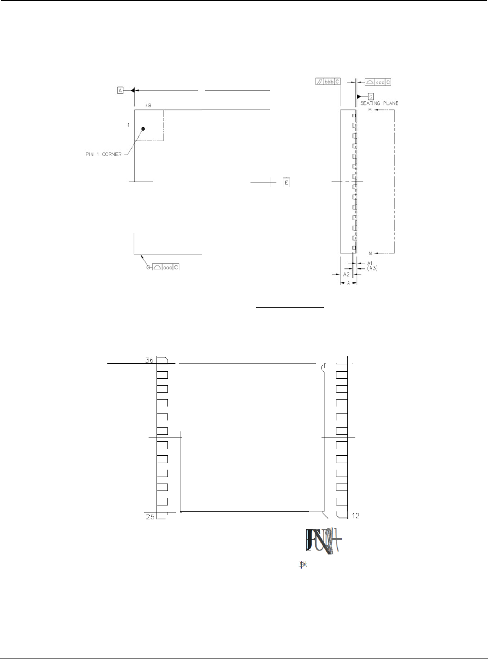
The EM358x package is a plastic 48-pin QFN that is 7 mm x 7 mm x 0.90 mm. Figure 6.2 illustrates the
package
drawing.
回
B
T
QP
V1
EW
|
令
l
eee
l
C
:.
3
1
U U
L
U
J U
_
U
P
B
"
1
仁
K
|
毛主
l
eee
l
c
A
丑
|
一一一一一一十一一一一一一
...
-
τ
/
2
J
山
鬥
門
「
鬥
鬥
|
t
;
J
X
:l
一
F
J
U
\
叭
\一
的
叮
沁
3
拈
叫
迂
E
S
況
嗨
E
吋
油
O
叫
…
B
C-
TO
叫
叫
F
'
N
1
+
I
d
::
d
)
C
1
|
‘
扒
r
忙
E
汀
T
凡心
C
H
λD
Figure
6.2.
Package
Drawing
50
Rev
1.0
..........
-
三
:
五
:
封
建

EM358x
Rev 1.0 51
Table 6.2. Package
Dimensions
Dimension
Min
Nom
Max
A
0.80 0.85 0.90
A1
0
0.035
0.05
A2
—
0.65 0.67
A3
0.203
REF
b
0.2 0.25 0.3
D
7
BSC
E
7
BSC
e
0.5
BSC
J
5.2 5.3 5.4
K
5.2 5.3 5.4
L
0.35 0.40 0.45
aaa
0.10
bbb
0.1
ccc
0.08
ddd
0.1
eee
0.1
Notes:
1. All dimensions shown are in millimeters (mm) unless
otherwise noted.
2. Dimensioning and Tolerancing per ANSI Y14.5M-1994.
3. This drawing conforms to the JEDEC Solid State Outline
MO-220, Variation VKKD-4.
4. Recommended card reflow profile is per the JEDEC/IPC J-
STD-020 specification for Small Body Components.
EM358x
52 Rev 1.0
MIN TYP
MAX
C1
C2
X1
X2
Y1
Y2
E
a0
a1
a2
b0
b1
b2
6.85
6.85
0.30
5.35
0.90
5.35
0.50
1.80
1.625
0.75
1.80
1.625
0.75
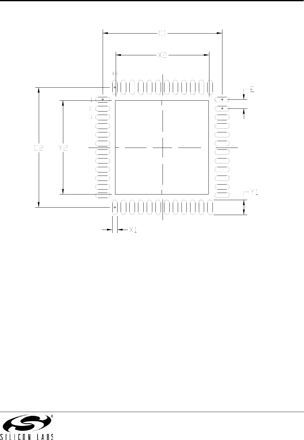
6.1.1. QFN48 Footprint Recommendations
Figure 6.3 demonstrates the IPC-7351 recommended PCB Footprint for the EM358x (QFN50P700X700X90-49N).
A ground pad in the bottom center of the package forms a 49th pin.
A 3 x 3 array of non-thermal vias should connect the EM358x decal center shown in Figure 6.3 to the PCB ground
plane through the ground pad. In order to properly solder the EM358x to the footprint, the Paste Mask layer should
have a 3 x 3 array of circular openings at 1.015 mm diameter spaced approximately 1.625 mm (center to center)
apart, as shown in Figure 6.4. This will cause an evenly distributed solder flow and coplanar attachment to the
PCB. The solder mask layer (illustrated in Figure 6.5) should be the same as the copper layer for the EM358x
footprint.
For more information on the package footprint, please refer to the appropriate EM358x Reference Design.
X2
Via Drill DIA =
0.254mm
b2
b0
a1
E
b1
C2
Y2
Y1
a2
X1
a0
C1
* Dimensions in
mm
* Dimensions are
for
Figures 19-2,
19-3
and
19-4
Figure 6.3. PCB Footprint for the EM358x
a0
a1
DIA = 1.01mm
b0
b1
C2
Y1
E X1
C1
Figure 6.4. Paste
Mask
EM358x
Rev 1.0 53
Figure 6.5. Solder Mask Dimensions

EM358x
54 Rev 1.0
Table 6.3. PCB Land
Pattern
Dimension
Min
Max
C1
6.80
6.90
C2
6.80
6.90
E
0.50
BSC
X1
0.20
0.30
X2
5.20
5.40
Y1
0.75
0.85
Y2
5.20
5.40
Notes:
General
1. All dimensions shown are in millimeters (mm) unless otherwise noted.
2. This Land Pattern Design is based on the IPC-7351 guidelines.
Solder Mask Design
1. All metal pads are to be non-solder mask defined (NSMD). Clearance between the solder mask and the metal pad is
to be 60mm minimum, all the way around the pad.
Stencil Design
1. A stainless steel, laser-cut and electro-polished stencil with trapezoidal walls should be used to assure good solder
paste release.
2. The stencil thickness should be 0.125 mm (5 mils).
3. The ratio of stencil aperture to land pad size should be 1:1 for all perimeter pads.
4. A 4x4 array of 1.1 mm square openings on 1.3 mm pitch should be used for the center ground pad.
Card Assembly
1. A No-Clean, Type-3 solder paste is recommended.
2. The recommended card reflow profile is per the JEDEC/IPC J-STD-020C specification for Small Body Components.
6.1.2. Solder Temperature Profile
Figure 6-6 illustrates the solder temperature profile for the EM358x. This temperature profile is similar for other
RoHS compliant packages, but manufacturing lines should be programmed with this profile in order to guarantee
proper solder connection to the PCB.

EM358x
Rev 1.0 55
The final end product must be labeled in a visible area with the following: “Contains FCC
ID: NHS-EM3585”, “contains IC: 3653A-EM3585”. The grantee's FCC ID can be used only
when all FCC/ IC compliance requirements are met.