Powerwave Technologies 5JS0077 Multi-Carrier RF Power Amplifier User Manual
Powerwave Technologies Inc Multi-Carrier RF Power Amplifier Users Manual
Users Manual

EHP19
Installation and
Service Manual
044-05210 Rev. A
September 2005
Integrated Power Transceiver
PRELIMINARY

© 2005 Powerwave Technologies Incorporated. All rights reserved.
Powerwave Technologies, and the Powerwave logo are registered trademarks.
This Powerwave product is intended only for installation in a RESTRICTED ACCESS LOCATION.
This Powerwave product is designed to operate within the normal operating (typical operating) ranges
or conditions specified in this document. Operation of this equipment beyond the specified ranges in
this document may cause:
• spurious emissions that violate regulatory requirements.
• the equipment to be automatically removed from service when maximum thresholds are exceeded.
• the equipment to not perform in accordance with its specifications.
It is the responsibility of the operator to ensure this equipment is properly installed and operated within
Powerwave operating specifications to obtain proper performance from the equipment and to comply
with regulatory requirements.

044-05205 Rev. A i
Warnings, Cautions, and Notes
Warnings, Cautions, and Notes are found throughout this manual where applicable. The associated
icons are used to quickly identify a potential condition that could result in the consequences described
below if precautions are not taken. Notes clarify and provide additional information to assist the user.
WARNING: This warning symbol means danger. You are in a situation that could cause
bodily injury or death. Before working on any equipment, be aware of the hazards involved
with electrical and RF circuits and be familiar with standard practices for preventing
accidents.
CAUTION: The caution symbol means reader be careful. In this situation, the user might do
something that could result in equipment damage or loss of data.
NOTE NOTE: The note symbol means reader take note. Notes contain helpful suggestions or
references to material not covered in this document. Procedures are not contained in notes.

ii 044-05205 Rev. A
Revision Record
Revision Letter Date of Change Reason for Change
Rev. A September, 2005 Preliminary Release

044-05210 Rev. A 1-1
Chapter 1
Product Description
1.1 Introduction
This manual contains information and procedures for the installation, operation, and maintenance of
the EHP19 Integrated Power Transceiver (IPT).
1.2 Scope of Manual
This manual is intended for use by service technicians familiar with similar types of equipment. It
contains service information required for the equipment described and is current as of the printing
date. Changes which occur after the printing date may be incorporated by a complete manual revision
or alternatively as additions.
The manual is organized into the following chapters:
• Chapter 1 - Product Description
• Chapter 2 - Installation
• Chapter 3 - Operation
• Chapter 4 - Maintenance
• Chapter 5 - Specifications and Drawings
1.3 Functional Description
The IPT is a high efficiency RF single channel power amplifier with an internal analog pre-distorter for
use with the Radio Base Station (RBS) digital pre-distorter system for RF output linearity. The IPT has
an operational bandwidth of 60 MHz from 1930 MHz to 1990 MHz producing a typical output of 60.2
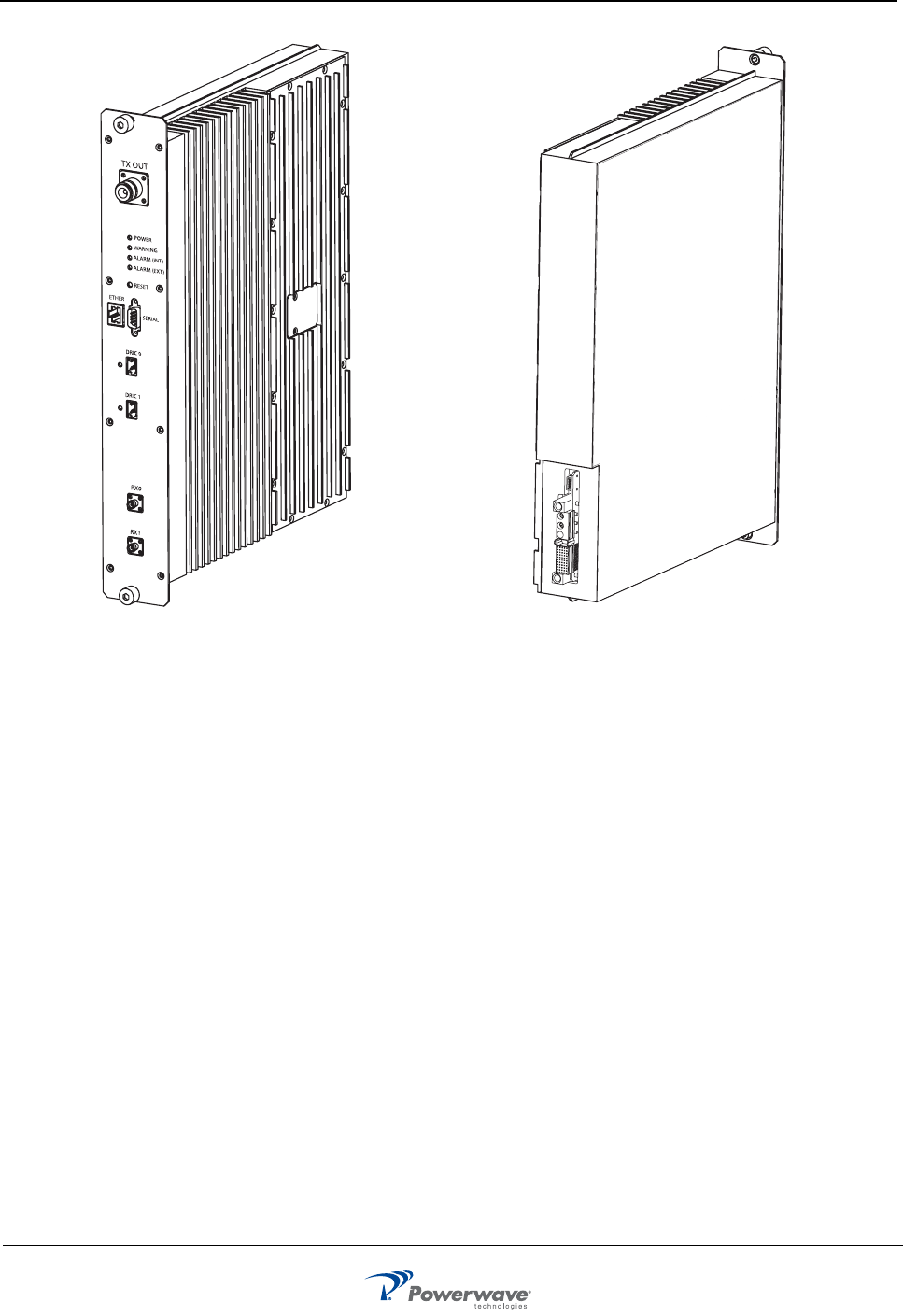
watts (47.8 dBm). The IPT is shown in Figure 1-1. Detailed functional and physical specifications for
the IPT are listed in Chapter 5.
1.3.1 RF Interface
The IPT RF interfaces consist of the TX OUT port located on the top of the IPT front panel and the
RX0 and RX1 ports located on the bottom of the IPT front panel.
1.3.2 Main Transceiver
The following circuits are part of the main transceiver section.
1.3.2.1 Customer Interface/CPRI Input
The incoming serial data stream from the customer interface (DRIC) front panel connector is applied
to a Serialiser-Deserialiser (SerDes), converted into a parallel format and decoded. The customer
interface also includes processing of the frame alignment, byte alignment and chip alignment,
including delay adjustment. A clock acts as the frequency reference for the entire transmitter. The
clock is extracted from the incoming signal using a phase locked loop (PLL). There are two outputs

Functional Description
1-2 044-05210 Rev. A
from this block: control data and signal data. The control data determines parameters such as
channel frequencies, signal ramp-up/ramp down and transmit power level. These functions are
implemented in a Field Programmable Gate Array (FPGA).
1.3.2.2 Digital Up Converter (DUC)
The DUC modulates individual symbol streams from the signal data stream on to baseband carriers
and applies root-raised cosine channel filtering. This function is implemented on an Application-
Specific Standard Product (ASSP).
1.3.2.3 Crest Factor Reduction (CFR)
The CFR function is implemented in the FPGA. The CPR varies the DUC signals to reduce the peak-
to average power of the transmit signal to allow the P-Mod to operate with higher efficiency ensuring
the transmit signals stay in the occupied bandwidth/spectral mask limits.
1.3.2.4 Data Interpolation (INT)
The interpolation function, which is implemented in the FPGA, changes the sampling rate up to 92.16
Msps.
1.3.2.5 Digital Predistortion (DPD)
The DPD function, which uses an ASSP DPD engine, and a Digital Signal Processor (DSP),
processes the forward path signal to compensate for the non-linearities in the forward path. The DPD
function ensures that the transmitter operates at the correct power level over variations in supply
voltage, load impedance, temperature and aging.
The DPD function also provides compensation for imperfections in the AUC such as differential delay,
I-Q amplitude and phase balance and DC offset/carrier leakage. the linearisation lock function
monitors the operation of the signal and turns off the transmitter if the system is not functioning
correctly. The digital output signal from the DPD engine is converted back to an analog signal in a
high-speed digital-to-analogue converter (DAC).
1.3.2.6 Analog Up Converter (AUC)
The AUC uses a direct-conversion architecture (I-Q modulator) to transform the I-Q baseband signals
from the DPD up to the operating RF frequency.
1.3.2.7 Observation Path (OBS)
The OBS act as a high performance radio receiver tuned to the RF transmit frequency. The OBS
converts the sampled RF transmit signal to a VHF intermediate frequency where it is sampled by a
high-speed analogue-to-digital converter (ADC). The output of the ADC is fed to the DPD block,
compared with the drive signal and then used to update the parameters in the DPD algorithms
running on the DSP.
1.3.2.8 Clock Module
The FPGA high-speed serial interface (SerDes) extracts a timing clock from the incoming data
stream, the transmit frequency stability depends on the accuracy of the incoming input signal. The
recovered clock is used to synchronize a crystal oscillator used as a clean frequency reference for the
timing functions on the TRx board (RF LOs, DAC and ADC clocks, Tx, Rx and lineariser signal
processing clocks).
The reference is used as a direct reference for the RL local oscillators. Except for the digital clocks,
the reference is passed to a PLL VCO, which is then subdivided. All RF PLLs include lock-detect
signals to allow the transmitter to be turned off if there is a fault with a PLL.
Functional Description
044-05210 Rev. A 1-3
1.3.3 Power Module
The P-Mod is a multi-stage amplifier, which amplifies the low level signal from the AUC up to the RF
output power level of +47.8 dBm (60.25 W). The P-Mod consists of a two-stage pre-driver, a driver
amplifier and an output stage. The bias currents are electronically calibrated during factory test and
bias setting and temperature compensation are controlled by a master control unit on the P-Mod
PCB. The P-Mod also includes a directional coupler, which allows a sample of the transmit signal to
be fed to the observation path and an isolator, which protects the P-Mod from damage or potential
oscillation under adverse RF load conditions. An RF switch allows either the observation signal or the
reflected power from the antenna connector, measured at the third port of the isolator, to be passed to
the TRx
1.3.4 Front Panel
The front panel contains a RESET switch and four status and alarm LEDs.
Figure 1-1 Integrated Power Transceiver Front and Rear Isometric View
FRONT REAR

Functional Description
1-4 044-05210 Rev. A
1.3.5 Operational States
The IPT has three operational states: Operational, Disabled and Not Ready.
The IPT remains in the Not Ready state during start-up until all parameters are met for the IPT to
become operational.
The IPT is normally in the Operational state: no faults are present, the IPT internal temperature is
within limits, appropriate DC power is applied, and the IPT is producing RF output. The green
operational (O) LED on the Man Machine Interface is lit.
The Disabled state is ordered from the RBS (if there is a fault in the IPT or in other RBS units) or
entered automatically when a critical hardware error is detected by the IPT. The Disabled state
causes the IPT to shut down, but it can be enabled by the RBS if the fault is cleared.
1.3.6 State Transitions
The IPT has five state transitions: Reset, Status OK, Alarm, Disable, and Enable.
Reset initiates the Not Ready state. This state is entered when power is initially applied to the IPT or
from a dedicated reset signal from the RBS to the IPT.
Status OK is entered from the Not Ready state and initiates the Operational state when commanded
by the IPT
Alarm initiates the Disabled state from the Operational state if the IPT detects a hardware or
temperature fault. The RBS reads the potential fault cause for fault logging.
Disable is ordered from the RBS to force the IPT to go to the Disabled state and shut down. Power on
of the IPT after a Disable can only be ordered by the RBS through a RESET command.
Enable is ordered from the RBS to power on the IPT after it has been disabled. The IPT enters the
Operational state after checking status and temperatures and re-perform start-up if required.
1.3.7 DC Power (DC)
DC power (-48 Vdc nominal) is supplied by the RBS to the IPT through the rear mounted connector.
Refer to Table 1-1 for a description of the DC connector inputs.
1.3.7.1 Power Supply
The power supply assembly contains two subassemblies. The DC/DC converter produces regulated
+28 Vdc, +9 Vdc and +6.5 Vdc from the -48 Vdc supply for the IPT internal supply. The low voltage
supply uses the +6.5 Vdc from the DC/DC converter to provide regulated 3.3 Vdc, 1.8 Vdc and 1.5
Vdc reference level supplies.
Table 1-1 DC Power Connections
Pins Signal Name Description
1,2 GND (-48V_RTN) DC plus (isolated from amplifier chassis)
3,4 -48V DC minus (isolated from amplifier chassis)
5,6 GND (NC) Not connected

Functional Description
044-05210 Rev. A 1-5

1-6 044-05210 Rev. A
This page intentionally left blank.

044-05210 Rev. A 2-1
Chapter 2
Installation
2.1 Introduction
This chapter contains unpacking, inspection and installation instructions for the EHP19 Integrated
Power Transceiver (IPT).
• Carefully read and understand all material in the chapter prior to installation.
• Review any government and local codes applicable to this installation.
• Before operating the equipment, read the operating instructions in Chapter 3.
2.2 Unpacking and Inspection
Perform the steps in Table 2-1 to unpack and inspect the IPT.
2.2.1 Damaged Equipment
If the equipment is damaged, a claim should be filed with the carrier when the extent of any damage
is assessed. Contact the factory for a return material authorization (RMA). Refer to Chapter 4.
2.3 Installation Instructions
Perform the following to install the IPT.
Table 2-1 IPT Unpacking and Inspection Instructions
Step Action
1Carefully open the container and remove the IPT.
2Visually inspect the IPT for damage that may have occurred during shipment. Check for
evidence of water damage, bent or warped chassis, loose screws or nuts, or extraneous
packing material in connectors. If possible, inspect the equipment in the presence of the
delivery person.
3If possible, retain all packing material that can be reused for repackaging the components.
WARNING: Ensure the RF power has been removed from the RF input cable before
connecting the RF input cable.
Installation Instructions
2-2 044-05210 Rev. A
Table 2-2 IPT Installation
Step Action
1Carefully slide the IPT into the subrack.
2Secure the IPT in the subrack by tightening the thumbscrews.
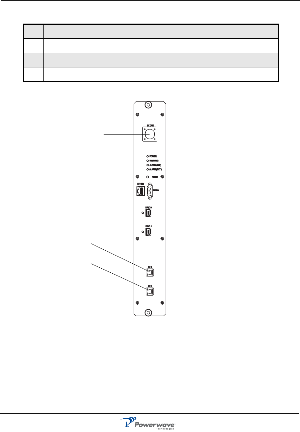
3Connect the TX cable, RX0 and RX1 cables as shown in Figure 2-1.
Figure 2-1 IPT Connector Locations
Transmit Output (TX)
Receive 0
(RX0) Input
Receive 1
(RX1) Input
044-05205 Rev A 3-1
Chapter 3
Operation
3.1 Introduction
This chapter contains operating instructions for the EHP19 Integrated Power Transceiver (IPT).
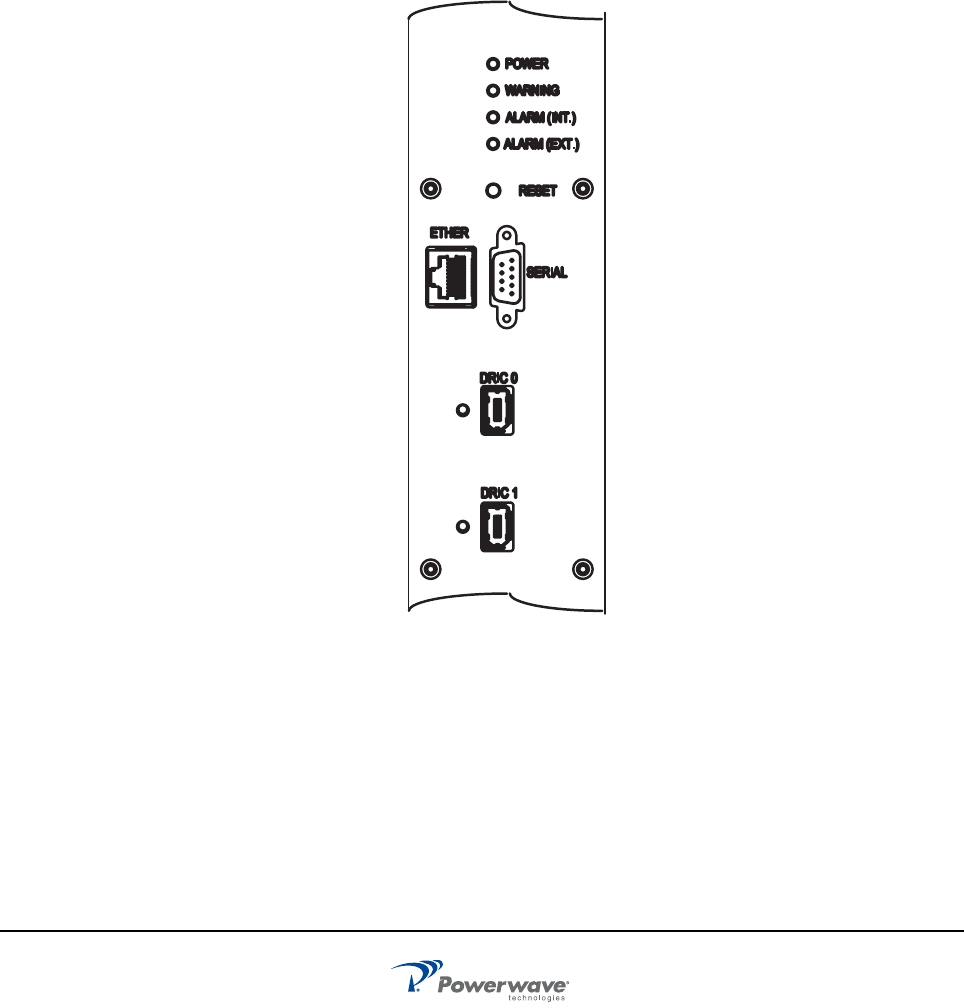
3.2 Controls and Indicators
The IPT provides one switch, four LED indicators, one ethernet connector, one serial connector and
two RS-485 connectors as shown in Figure 3-1.
3.2.1 Reset Switch
The Reset recessed pushbutton switch allows the operator to reset the IPT control circuits.
Figure 3-1 IPT Indicators and Controls

Initial Start-Up and Operating Procedures
3-2 044-05205 Rev. A
3.2.2 Status and Alarm Indicators
MCPA alarm conditions are reported to the system as logic level signals through the rear connector.
The front panel LED provides a visual reference for the operator of MCPA status. Refer to Table 3-1.
The IPT ALARM (INT.) lights when a IPT fault occurs. The IPT control logic provides the following
alarms to the RBS when a fault occurs:
• Temperature out of range
• Voltage out of range
• Current out of range
• Open circuit (reported as a voltage out or range alarm)
• Short circuit (reported as a current out of range alarm)
• Hardware fault. A hardware fault always requires removal and replacement of the IPT to resolve
the fault condition.
Some MCPA alarms are caused by faults external to the IPT such as an out of tolerance DC supply or
RF supply. A major fault will disable the RF output of the IPT, a minor fault has no effect on the RF
output. Conditions external to the IPT should be investigated before replacing the IPT.
3.3 Initial Start-Up and Operating Procedures
No operator action is required during start-up and normal operations: the IPT powers up when -48
Vdc power is applied, the IPT internal temperature is within operating range, no faults are present, RF
input and output are within specifications and the IPT is commanded to power up by the RBS logic. If
the IPT does not power up or the ALARM (INT.) LED stays lit, refer to Paragraph 4.3 for
troubleshooting instructions.
CAUTION: Before applying power, ensure the input and output of the system is properly
terminated at 50 ohms. Do not operate the system without a load attached. Refer to Chapter
5 for input power requirements, excessive input power may damage the IPT.

044-05210 Rev. A 4-1
Chapter 4
Maintenance
4.1 Introduction
This chapter contains the periodic maintenance, troubleshooting and removal and replacement
instructions for the EHP19 Integrated Power Transceiver (IPT).
4.2 Periodic Maintenance
Recommended periodic maintenance requirements are listed in Table 4-1.
4.3 Troubleshooting
Perform the instructions in Table 4-2 if the IPT becomes inoperative.
4.4 Module Field Replacement
The IPT should be removed and replaced only by a qualified technician with experience maintaining
RF power amplifiers and similar equipment.
NOTE Check your sales order and equipment warranty before attempting any service or repair activity.
Do not break the seals on equipment under warranty or the warranty will be null and void. Do not
return equipment for warranty or repair service until proper shipping instructions are received from
the factory. Refer to Paragraph 4.5.
Table 4-1 Recommended Periodic Maintenance
Task Interval Action
Inspection of cables and connectors 12 months Inspect signal and power connectors for frayed
insulation. Check RF connectors for tightness.
Cleaning As Required Clean as required depending on equipment operating
environment.
Table 4-2 Troubleshooting
Step Action
1 Press the IPT RESET button. Check to see if the fault clears.
2Check for proper DC supply voltage.
3 Verify all RF connections are tight.
4Verify that the MCPA does not have a major fault.
5 Contact your field representative or the factory if major fault does not clear.

Return For Service Procedures
4-2 044-05210 Rev A
4.4.1 IPT Removal and Replacement Procedure
Perform the following to remove and replace the IPT:
4.5 Return For Service Procedures
Perform the instructions in the following paragraphs to ensure optimum response when returning
products to Powerwave.
4.5.1 Obtaining An RMA
A Return Material Authorization (RMA) number must be obtained prior to returning equipment to the
factory for service. Contact Powerwave at (714) 466-1000 or send a fax to (714) 466-5800 for an
RMA number. Failure to obtain the RMA number can result in delays in receiving repair service.
4.5.2 Repackaging For Shipment
Reuse the original package designed for shipping the amplifier to ensure safe shipment of the
amplifier. Contact Powerwave for packing materials if the original packaging is not available.
WARNING: Ensure the RF power has been removed from the RF input cable before
disconnecting or reconnecting the RF input cable.
Table 4-3 IPT Removal and Replacement
Step Action
1 DIsconnect cables at the TX, RX0 and RX1 inputs.
2Loosen the thumbscrews and slide the IPT out of the subrack.
3 To replace the IPT, carefully slide the IPT back into the subrack slot, tighten the thumbscrews
and replace the RF cables.

044-05210 Rev A 5-1
Chapter 5
Specifications
5.1 Power Amplifier Unit (IPT) Specifications
Table 5-1 IPT Functional and Physical Specifications
Frequency Range 1925 to 1995 MHz
Instantaneous Bandwidth 5 MHz
Total Typical / Maximum Input Power 2.9 dBm (1.9 mW) typical / 12.0 dBm (15.8 mW) maximum
Total Output Power 26.3 watts typical / 33.1 watts maximum
Adjacent Channel Leakage Power Ratio ACLR1 less than -33.5 dBc
ACLR2 less than -54.8 dBc
RF Gain 42.3 dB +/- 2 dB over the frequency and temperature range
Gain Flatness Less than 1.5 dB
Output Protection Mismatch protected
Input Port Return Loss Less than -15 dB
Harmonics Less than -34 dBm / 1 Mhz
Out of Band Spurious Lower -27 dBm / Higher -27 dBm
Duty Cycle Continuous
DC Input Power From -57.0 Vdc to -38.5 Vdc (-48 Vdc nominal)
Current limit is 8 amps maximin for less than 10 milliseconds
Operating Temperature -33 to +45 °C Normal Operation
-45 to +55 °C Exceptional Operation*
-50 to +60 °C Nondestructive Operation**
Storage Temperature -25 to +55 °C
Operating Humidity 15 to 100% Normal Operation
8 to 100% Exceptional Operation*
5 to 100% Nondestructive Operation**
Storage Humidity 10 to 100 per cent
RBS / IPT communication Dual I²c serial bus, 0 to 100 KHz baud rate
RF Input Connector SMA-Female
RF Output Connector SMA-Female
Power Consumption Less than 207 watts maximum during normal operation
186 watts typical, 60 watts maximum at low temperature start
Weight 7.3 lbs. (3.3 kg.)
Dimensions 14.6 in. (37.1 cm) wide by 2.1 in. (5.3 cm) high by 9.8 in. (24.9 cm) deep

5-2 044-05210 Rev A
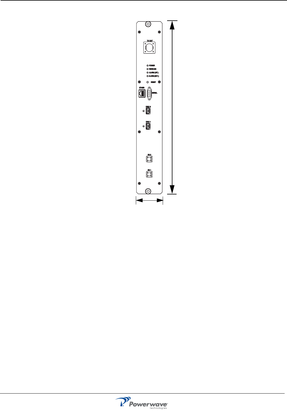
Figure 5-1 Model EHP19 IPT Front View
in
in

044-05210 Rev. A 5-3
Figure 5-2 Model EHP19 IPT Side View
in

5-4 044-05210 Rev A

044-05210 Rev A 5-1
Chapter 5
Specifications
5.1 Specifications
Table 5-1 IPT Functional and Physical Specifications
Frequency Range 1930 to 1990 MHz
Instantaneous Bandwidth 15 MHz
Total Typical / Maximum Input Power N/A
Total Output Power 60.2 watts (47.8 dBm) typical
Adjacent Channel Leakage Power Ratio ACLR1 less than -33.5 dBc
ACLR2 less than -54.8 dBc
RF Gain N/A
Gain Flatness Better than +/- 0.5 dB
Output Protection Mismatch protected
Input Port Return Loss N/A
Harmonics Less than -34 dBm / 1 Mhz
Out of Band Spurious Lower -27 dBm / Higher -27 dBm
Duty Cycle Continuous
DC Input Power From -57.6 Vdc to -38.4 Vdc (-48 Vdc nominal)
Current limit is 10.1 amps, 9.8 amps typical (at -48 Vdc)
Operating Temperature -33 to +45 °C Normal Operation
-45 to +55 °C Exceptional Operation*
-50 to +60 °C Nondestructive Operation**
Storage Temperature -25 to +55 °C
Operating Humidity 15 to 100% Normal Operation
8 to 100% Exceptional Operation*
5 to 100% Nondestructive Operation**
Storage Humidity 10 to 100 per cent
RBS / IPT communication
RF Input Connector SMA-Female
RF Output Connector SMA-Female
Power Consumption Less than 207 watts maximum during normal operation
186 watts typical, 60 watts maximum at low temperature start
Weight 7.3 lbs. (3.3 kg.)
Dimensions Refer to Figure Figure 5-1 and Figure 5-2

5-2 044-05210 Rev A
Figure 5-1 EHP19 IPT Side View
290 mm
357 mm
044-05210 Rev. A 5-3
Figure 5-2 EHP19 IPT Front View
356 mm
59 mm

5-4 044-05210 Rev A

Corporate Headquarters
Powerwave Technologies, Inc.
1801 East St. Andrew Place
Santa Ana, CA 92705 USA
Tel: 714-466-1000
Fax: 714-466-5800
www.powerwave.com
Main European Office
Antennvägen 6
SE-187 80 Täby
Sweden
Tel: +46 8 540 822 00
Fax: +46 8 540 823 40
Main Asia-Pacific Office
23 F Tai Yau Building
181 Johnston Road
Wanchai, Hong Kong
Tel: +852 2512 6123
Fax: +852 2575 4860
©Copyright March 2005, Powerwave Technologies, Inc. All Rights reserved. Powerwave, Powerwave Technologies, The Power in Wireless and the Powerwave logo are registered trademarks of Powerwave Technologies, Inc.
Powerwave Installation and Service Manual