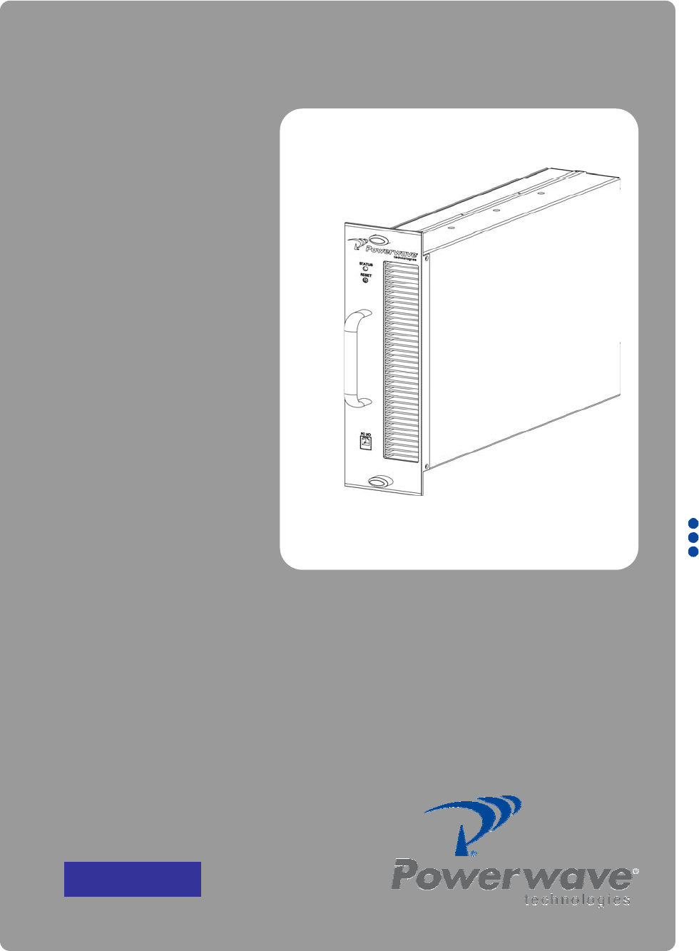
Powerwave Technologies 5JS0078 Multi-Carrier RF Power Amplifier User Manual G3H 851 80 Manual
Powerwave Technologies Inc Multi-Carrier RF Power Amplifier G3H 851 80 Manual
Users Manual
Installation and
Service Manual
G3H-851-80 Multi-Carrier
Power Am
p
lifie
r
044-05xxx Rev A
November 2005

044-05xxx Rev A
© 2005 Powerwave Technologies, Incorporated. All rights reserved.
Powerwave Technologies and the Powerwave logo are registered trademarks
Powerwave Technologies, Inc. reserves the right to make changes to the documentation and equipment
including, but not limited to, component substitution and circuitry changes. Changes that impact this
manual may subsequently be incorporated in a later revision of this manual.
This Powerwave product is designed to operate within the Normal Operating (typical operating) ranges or
conditions specified in this document. Operation of this equipment beyond the specified ranges in this
document may cause (1) spurious emissions that violate regulatory requirements; (2) the equipment to be
automatically removed from service when maximum thresholds are exceeded; or (3) the equipment to not
perform in accordance with its specifications. It is the Operator's responsibility to ensure this equipment is
properly installed and operated within Powerwave operating specifications to obtain proper performance
from the equipment and to comply with regulatory requirements.

044-05xxx Rev A i
Warnings, Cautions, and Notes
Warnings, cautions, and notes are found throughout this manual. The associated icons in warnings and
cautions are used to quickly identify a potential condition that could result in the consequences described
below if precautions are not taken. Notes clarify and provide additional information to assist the user.
WARNING This warning symbol means danger. You are in a situation that could
cause bodily injury. Before you work on any equipment, be aware of the
hazards involved with electrical and RF circuitry and be familiar with
standard practices for preventing accidents.
CAUTION This caution symbol means reader, be careful. In this situation, the user might do
something that could result in equipment damage or loss of data.
Note This note symbol means reader, take note. Notes contain helpful suggestions or
references to material not covered in the document. Procedures are not
contained in notes.

ii 044-05xxx Rev A
Revision Record
Revision Record
Revision Letter Date of Entry Reason for Change
A November, 2005 Original version of product

044-05xxx Rev A iii
Table of Contents
Chapter Number Title Page
Chapter 1 General Description 1-1
1-1 Introduction ................................................................................................................................1-1
1-2 General Description...................................................................................................................1-1
1-3 Functional and Physical Specifications .....................................................................................1-4
1-4 Ordering Information..................................................................................................................1-5
1-5 General Safety..............................................................................Error! Bookmark not defined.
1-5.1 Electronic Modules .......................................................................Error! Bookmark not defined.
Chapter 2 Installation 2-1
2-1 Introduction ................................................................................................................................2-1
2-2 Unpacking and Inspection .........................................................................................................2-1
2-3 Air Conditioning .........................................................................................................................2-1
2-4 Electrical Load ...........................................................................................................................2-2
2-5 Installation Instructions ..............................................................................................................2-3
2-5.1 Installing the Amplifier into the Sub-rack ...................................................................................2-3
2-5.2 Combo Connector......................................................................................................................2-4
Chapter 3 Operating Instructions 3-1
3-1 Introduction ................................................................................................................................3-1
3-2 Controls and Indicators..............................................................................................................3-1
3-2.1 RESET Switch ...........................................................................................................................3-1
3-2.2 LED Status Indicator and RESET/On/Off Toggle Switch ..........................................................3-1
3-2.3 RJ-11 PC Interface ....................................................................................................................3-2
3-3 Initial Start-Up and Operating Procedures.................................................................................3-2
Chapter 4 Principles of Operation................................................................... 4-1
4-1 Introduction ................................................................................................................................4-1
4-2 RF Input Signal ..........................................................................................................................4-1
4-3 RF Output Load .........................................................................................................................4-1
4-4 Functional Description ...............................................................................................................4-1
4-4.1 Preamplifier................................................................................................................................4-2
4-4.2 Main and Error Amplifiers ..........................................................................................................4-2
4-4.3 Alarm Monitoring and Control....................................................................................................4-2
4-4.4 First and Second Loop Control Circuits.....................................................................................4-3
4-4.5 Pilot Tone Generator .................................................................................................................4-3
4-5 Amplifier Module Cooling...........................................................................................................4-3
4-6 Power Distribution......................................................................................................................4-3
4-7 Amplifier Alarms.........................................................................................................................4-4

iv 044-05xxx Rev A
Chapter 5 Maintenance 5-1
5-1 Introduction ................................................................................................................................5-1
5-2 Periodic Maintenance ................................................................................................................5-1
5-3 Test Equipment Required For Test ...........................................................................................5-1
5-4 Amplifier Performance Test .......................................................................................................5-2
5-4.1 Amplifier Spurious Emissions Test:...........................................................................................5-2
5-4.2 Gain Test: ..................................................................................................................................5-3
5-4.3 Input Return Loss: .....................................................................................................................5-4
5-4.4 Test Data Sheet.........................................................................................................................5-5
5-5 Return For Service Procedures.................................................................................................5-5
5-5.1 Obtaining An RMA .....................................................................................................................5-5
5-5.2 Repackaging For Shipment .......................................................................................................5-5
Appendix A Abbreviations and Acronyms 1
List of Figures
Figure Number Figure Title Page
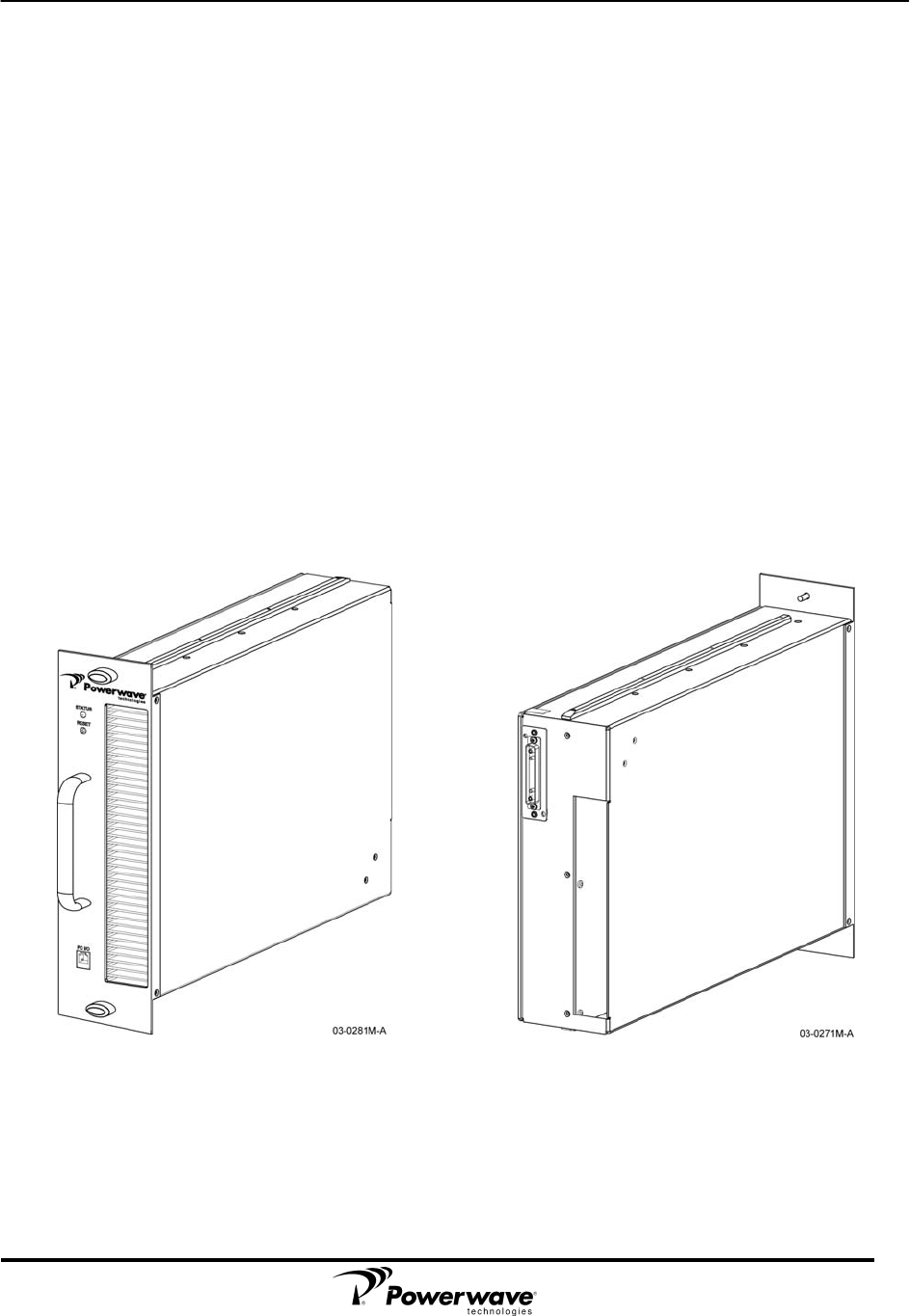
Figure 1-1. Model G3H-851-80 Amplifier – Front and Rear Isometric View..............................................1-1
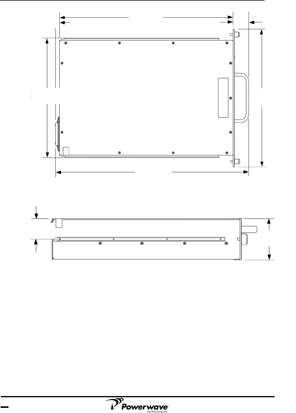
Figure 1-2. Model G3H-851-80 Amplifier Side View..................................................................................1-2
Figure 1-3. Model G3H-851-80 Amplifier Bottom View .............................................................................1-2
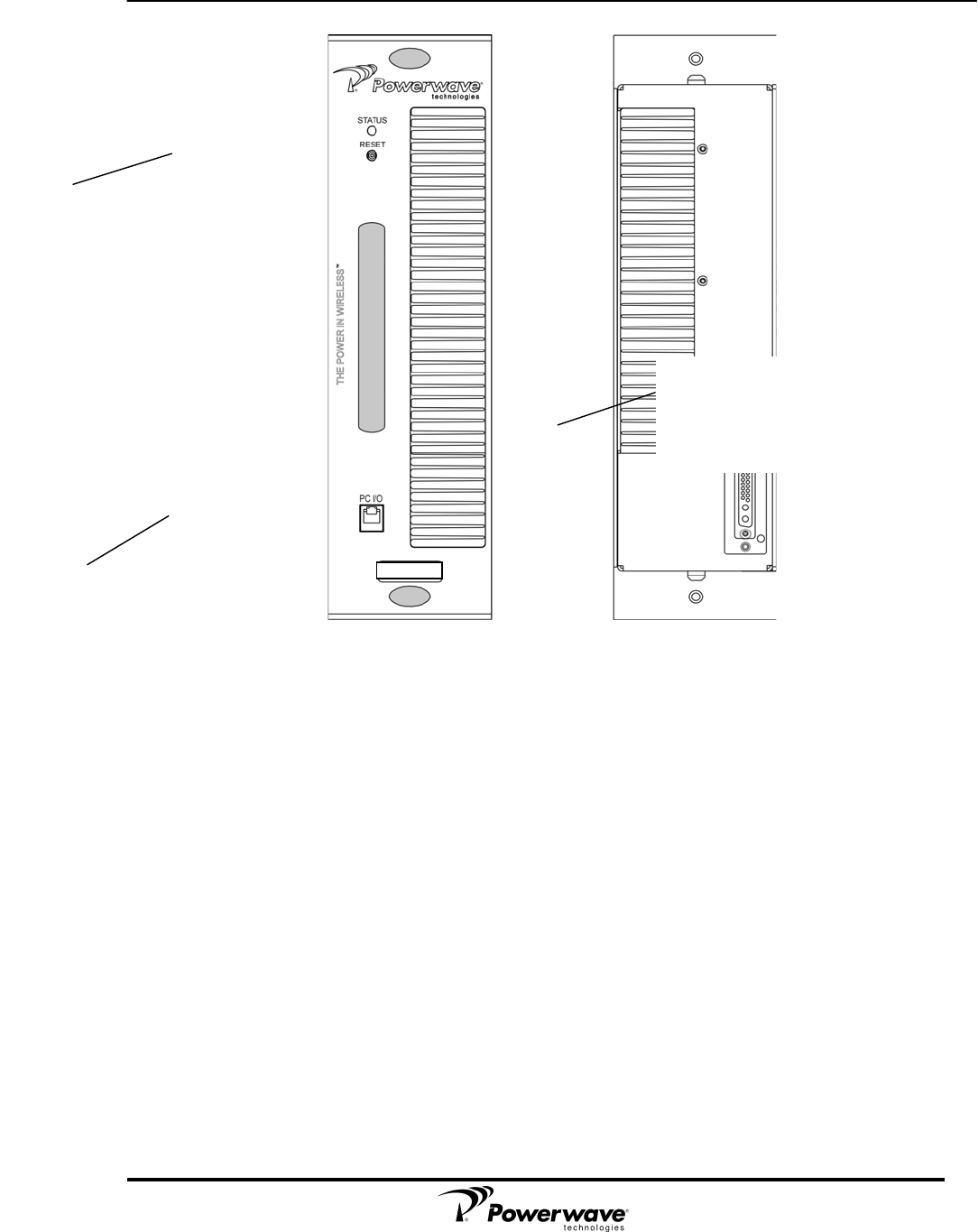
Figure 1-4. Model G3H-851-80 Amplifier Front Panel ...............................................................................1-3
Figure 2-1. Power Switch Functions and Unlocking/Locking Thumbscrews.............................................2-3
Figure 2-2. Combo Connector (Male, on Rear of G3H-851-80 Amplifier Module) ....................................2-4
Figure 3-1. G3H-851-80 Controls and Indicators ......................................................................................3-1
Figure 4-1. Functional Block Diagram .......................................................................................................4-2
Figure 5-1. Amplifier Test Setup Diagram – Configuration A ....................................................................5-3
Figure 5-2. Amplifier Test Setup – Configuration B ..................................................................................5-4
List of Tables
Table Number Table Title Page
Table 1-1. G3H-851-80 Amplifier Specifications........................................................................................1-4
Table 1-2. Major System Components .....................................................................................................1-5
Table 2-1. Averaged Heat Loading............................................................................................................2-2
Table 2-2. Averaged DC Current Load ......................................................................................................2-2
Table 2-3. G3H-851-80 Amplifier Combo Connector Specifications.........................................................2-4
Table 3-1. Status Indicator Colors and Status...........................................................................................3-2
Table 4-1. G3H-851-80 Alarm States ........................................................................................................4-4
Table 5-1. Periodic Maintenance ...............................................................................................................5-1
Table 5-2. Test Equipment Required.........................................................................................................5-1
Table 5-3. Amplifier Performance Data .....................................................................................................5-5
044-05xxx Rev A 1-1
Chapter 1
General Description
1-1 Introduction
This manual contains information and procedures for installation and servicing of Powerwave’s G3H-851-
80 Amplifier. The manual is organized into two chapters as follows:
Chapter 1 General Description Chapter 4 Principles of Operation
Chapter 2 Installation Chapter 5 Maintenance
Chapter 3 Operating Instruction Appendix A Glossary of Terms
1-2 General Description
The G3H-851-80 Power Amplifier, shown in Figure 1-1through Figure 1-4, operates in the 18 MHz
frequency band from 851 MHz to 869 MHz with an instantaneous bandwidth of not more than 18 MHz.
The instantaneous bandwidth is the maximum frequency band in which any two or more signals can
occupy .The amplifier’s instantaneous bandwidth is set automatically and does not require any manual
setup.
Front Rear
Figure 1-1. Model G3H-851-80 Amplifier Front and Rear Isometric View
044-05xxx Rev A
1-2
Figure 1-2. Model G3H-851-80 Amplifier Side View
Figure 1-3. Model G3H-851-80 Amplifier Bottom View
0.389 in.
(0.99 cm)
17.06 in.
(43.33 cm)
1.59 in.
(4.03 cm)
13.96 in.
(35.45 cm)
19.58 in.
(49.73 cm)
12.09 in.
(30.70 cm)
1.90 in.
(4.82 cm) 3.86 in.
(9.80 cm)
044-05xxx Rev A 1-3
Figure 1-4. Model G3H-851-80 Amplifier Front Panel
n
ESET
Combo
Connector –
Power. Alarms,
and RF I/O
RS-232
Port
044-05xxx Rev A
1-4
1-3 Specifications
Electrical, mechanical, and environmental specifications for the G3H-851-80 amplifier are listed in
Table 1-1.
Table 1-1. G3H-851-80 Amplifier Specifications
Frequency Range 851-869 MHz;
Maximum Instantaneous Bandwidth 18 MHz bandwidth (lowest to highest transmitted frequency)
Carrier Types IDEN, 1X-EVDO/IS-95
Minimum Channel Spacing 1.25 MHz for 1X-EVDO/IS-95, 30 kHz for iDEN
Total Maximum Input Power -11.69 dBm @ 80 Watts (to achieve rated power);
-11.01 dBm max. –5.7 dBm or greater causes input overdrive
shutdown.
Total Average Output Power 80 Watts @27Vdc, @+25 °C
DC/RF Conversion Efficiency > 16%
Intermodulation Distortion
and In-Band Spurious:
-63 dBc (Min) @ +26 to +28 Vdc @ 80 Watts; 600 KHz channel spacing
within 25 MHz bandwidth*
RF Gain at 869 to 894 MHz 63 dB +1 dB
Gain Flatness: +0.5 dB @ 26 – 28 Vdc
Gain Variation Over Temperature: +0.5 dB from 26 Vdc to 28 Vdc over -20 to +50 °C
Output Protection: Mismatch protected
Input Port Return Loss: 11 dB
Out of Band Spurious: Better than –60 dBc, +26 Vdc to +28 Vdc
Spurious Performance ITU-R SM329-9, Category A, non-carrier related
Duty Cycle: Continuous
DC Input Voltage:
DC Input Current:
+27 Vdc ± 1 Vdc, operational range +21.0 Vdc to 30 Vdc amplifier will
disable at < 20.5 Vdc or > +30.5 Vdc.
26.5 Amps typical @ 80 W out,
28 A max @ 80 Watts (over temperature or over voltage);
Operating Temperature: -33 ºC. to +50 ºC.
Storage Temperature: -40 ºC. to +85 ºC.
Operating Humidity: 5 % to 95 % relative humidity (non-condensing)
Storage Humidity: 5 % to 95 % relative humidity (non-condensing)
Altitude -50 to +4000 M (-164 to 13,125 ft.)
RF Input / Output / Status / Alarm /
Control / DC Input Connectors: 21-Pin D-Subminiature combo connector
Maintenance Port RJ-11, RS-232 (for factory use only)
Continued next page
Switches Reset/On/Off Switch
044-05xxx Rev A 1-5
Indicators:
STATUS LED; Green (normal), Yellow (minor alarm), Red (critical alarm)
Dimensions: 35.46 cm wide, 9.56 cm high, 45.0 cm deep (including handles)
Weight: 13 kg (28.6 lb.)
Note This Powerwave product is designed to operate within the normal operating (typical
operating) ranges or conditions specified in this document. Operation of this equipment
beyond the specified ranges may cause (1) spurious emissions that
violate regulatory requirements; (2) the equipment to be automatically removed from
service when maximum thresholds are exceeded; or (3) the equipment to not perform in
accordance with its specifications. It is the operator's responsibility to ensure this
equipment is properly installed and operated within Powerwave operating specifications to
obtain proper performance from the equipment and to comply with
regulatory requirements. Industry Canada: The Manufacturer's rated output power of this
equipment is for single carrier operation. For situations when multiple carrier signals are
present, the rating would have to be reduced by 3.5 dB, especially where the output
signal is re-radiated and can cause interference to adjacent band users. This power
reduction is to be by means of input power or gain reduction and not by an attenuator at
the output of the device.
1-4 Ordering Information
Table 1-2 lists major system component numbers and descriptions for use in ordering.
Table 1-2. Major System Components
Model Number Description
G3H-851-80 80-Watt Amplifier, +27 Vdc
*Amplifier sub-racks sold and described separately

044-05xxx Rev A
1-6
(Page intentionally left blank)

044-05177 Rev A 2-1
Chapter 2
Installation
2-1 Introduction
This chapter contains unpacking, inspection, and installation instructions for the G3H-851-80 Multi-Carrier
Power Amplifier (MCPA). Carefully read all material in this chapter prior to equipment installation. Also,
read and review the operating procedures in chapter 3 prior to installing the equipment.
2-2 Unpacking and Inspection
This equipment has been operated, tested, and calibrated at the factory. Only in the event of severe
shocks or other mistreatment should any substantial readjustment be required. Carefully unpack each
piece of equipment after it has reached the installation site and is approximately in place. Carefully open
the amplifier containers and remove the contents. Inventory all items to ensure all needed materials have
been delivered.
Retain all packing material to support any claim of shipping damage or for use in the event that the
equipment must be returned to the factory.
CAUTION Exercise care in handling equipment during inspection to prevent damage
caused by rough or careless handling.
Visually inspect the Amplifier for damage that may have occurred during shipment as follows:
1. Inspect the MCPA for damage that may have occurred during shipment.
2. Check for evidence of water damage, bent or warped chassis, loose screws or nuts, or extraneous
packing material in the connector(s).
CAUTION Before applying power, make sure that all connectors are secure. Make sure that the
input and output are properly terminated at 50 ohms. Do not operate the amplifier
without a load attached. Refer to Table 1-1 for input power requirements. Excessive
input power may damage the equipment.
If the equipment is damaged:
• The carrier is your first area of recourse.
• A claim should be filed with the carrier once the extent of any damage is assessed. We cannot
stress too strongly the importance of IMMEDIATE careful inspection of the equipment and the
subsequent IMMEDIATE filing of the necessary claims against the carrier, if necessary.
If the equipment is damaged and must be returned to the factory:
• Please write or phone for return authorization.
• Powerwave may not accept returns without a return authorization.
2-3 Air Conditioning
Each G3H-851-80 amplifier generates 1981 BTU/hour of heat at full 80-Watt power. A 1-ton air
conditioner offsets 12,000 BTUs per hour of heat. Each sub-rack, exclusive of amplifiers, generates
2-2 044-05177 Rev A
approximately 42 BTU per hour of heat. The G3H-851-80 amplifier is designed to operate within the
extended low temperature and high temperature environments defined in Table 1-1.
Table 2-1 describes the heat load (at 80 Watts typical) for a 3-sector (70%), 2-sector (80%), omni (90%),
and typical (100%) site. Perform a site survey to determine actual air conditioning needs.
Table 2-1. Averaged Heat Loading
Amplifier
Power No. Of
Amplifiers 3-Sector (70%)
Averaged
BTU/hour
2-Sector (80%)
Averaged
BTU/hour
1-Sector (90%)
Averaged
BTU/hour
100%
Typical
80 4 6,956 7,924
80 3 5,217 5,565 5,943
80 2 3,478 3,710 3,806 3,962
80 1 1,739 1,855 1,903 1,981
2-4 Electrical Load
Table 2-2 lists the current consumption at 27 Vdc.
Table 2-2. Averaged DC Current Load
Amplifier
Power No. Of
Amplifiers 3-Sector (70%)
Averaged Current 2-Sector (80%)
Averaged Current 1-Sector (90%)
Averaged Current 100%
Typical
80 4 88.8 A 106 A
80 3 66.6 A 72.6 A 79.5 A
80 2 44.4 A 48.4 A 50.2 A 53 A
80 1 22.2 A 24.2A 25.1 A 26.5 A
044-05177 Rev A 2-3
2-5 Installation Instructions
Install the G3H-851-80 amplifier as follows:
WARNING Turn off external primary DC power before connecting DC power
cables.
2-5.1 Installing the Amplifier into a Sub-rack
1. Inspect the 21WA4 male combo connector (Figure 2-2) on the rear of each amplifier. Verify that all
pins are straight, no pins are recessed, packing material is removed, and that the alignment shield is
not bent.
2. Set the power Reset/On/Off switch on each amplifier to “Off” (down position) as shown in Figure 2-1.
CAUTION Do not slam or force the amplifier into the sub-rack. This may cause the pins
on the combo connector of the amplifier to become recessed or broken.
3. With the thumbscrews in the unlock position, install the amplifier(s) into the sub-rack, positioning
each in accordance with the information in the system manual. Turn the top and bottom thumbscrews
to the lock position as shown in Figure 2-1 to secure the amplifier(s) in the sub-rack.
WARNING Check your work before applying DC voltage to the amplifier. Make
certain all connections are tight and correct.
4. Measure primary DC input voltage. DC input voltage should be +27 Vdc ±1.0 Vdc. If the DC input
voltage is above or below the limits, call and consult an electrician before you turn on your amplifier
system.
5. Refer to Chapter 3 for initial turn-on and checkout procedures.
Figure 2-1. Power Switch Functions and Unlocking/Locking Thumbscrews
3-Position Switch:
Reset (Up)
On (Middle)
Off (Down)
Unlocked
Position
Locked
Position
2-4 044-05177 Rev A
2-5.2 Combo Connector
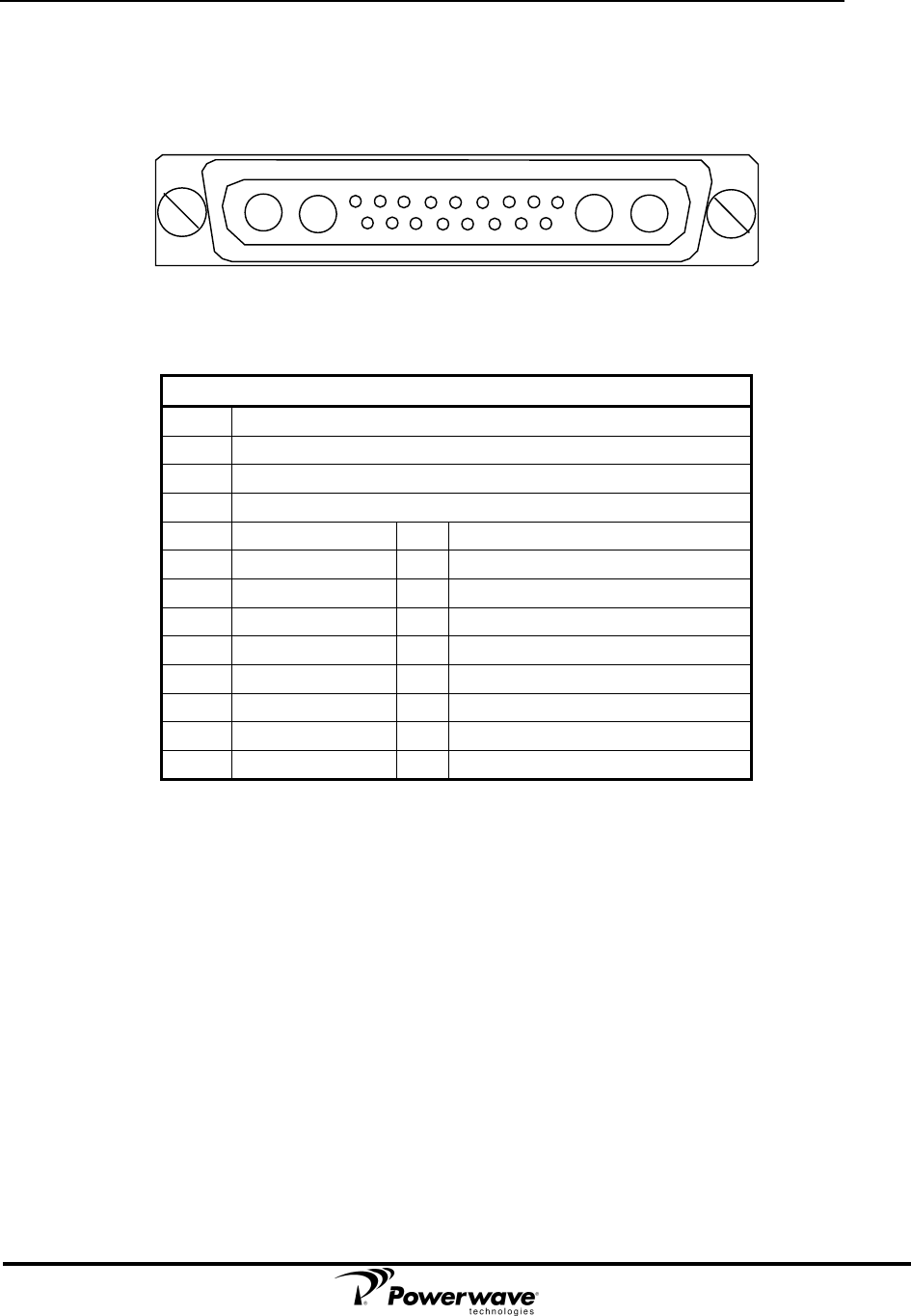
The power, alarm, control, and RF connections on the amplifier are made through a 21WA4 male
connector, located on the rear of the amplifier. Pins are listed and described in Table 2-3. Alarms are
interpreted by the amplifier sub-rack and reported to the base station as a system level alarm.
A1 A2 A3 A4
1 2 3 4 5 6 7 8 9
10 11 12 13 14 15 16 17
Figure 2-2. Combo Connector (Male, on Rear of G3H-851-80 Amplifier Module)
Table 2-3. G3H-851-80 Amplifier Combo Connector Signal List
Pins/Signal Names
A1 RF Input (Coaxial Contact)
A2 +27 Vdc (Power Contact)
A3 Ground (Power Contact)
A4 RF Output (Coaxial Contact)
1 TX H (RS-485) 10 System Reset TTL
2 TX L (RS-485) 11 NC
3 GND 12 NC
4 RX H (RS-485) 13 AMP AO
5 RX L (RS-485) 14 AMP A1
6 GND 15 AMP A2
7 MOD_DET 16 NC
8 Summary Fault 17 MCPA Temp
9 DC (On/Off)
044-05177 Rev A 3-1
Chapter 3
Operating Instructions
3-1 Introduction
This chapter contains a description of the G3H-851-80 Multi-Carrier Power Amplifier (MCPA)
controls, indicators, and initial start-up and operating procedures.
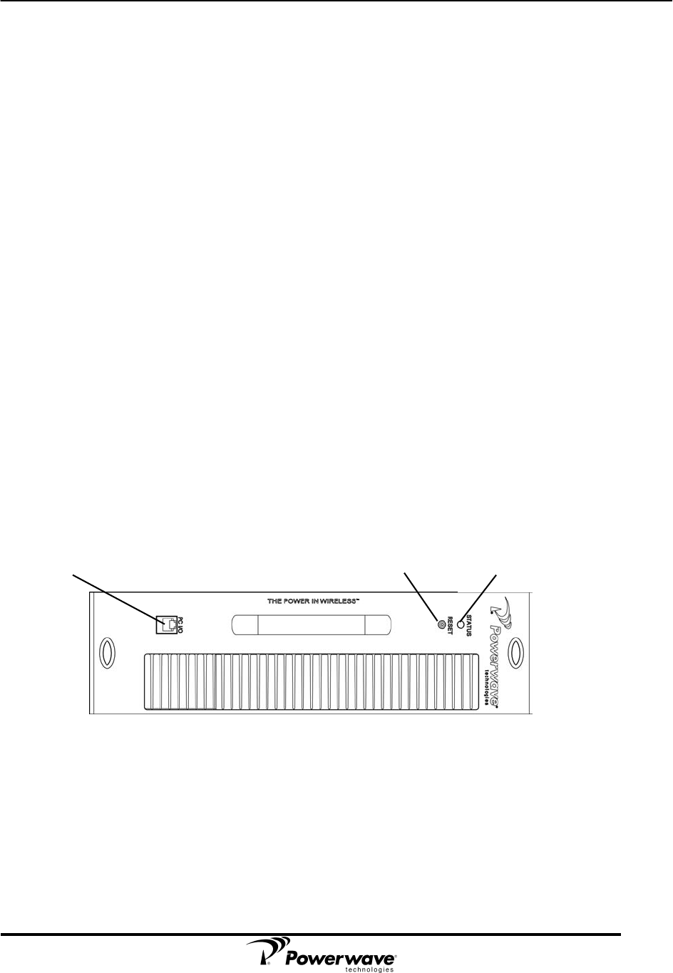
3-2 Controls and Indicators
The controls and indicators for the G3H-851-80 Power Amplifier consist of the primary power
RESET toggle switch, the LED STATUS indicator, and the RJ-11 PC Interface as shown in
Figure 3-1.
3-2.1 RESET Switch
The RESET Switch, located on the front panel, has three positions, each with its own function.
• The momentary up position resets fault indications and returns the MCPA to normal
operation if a critical or hard fault does not prevent such operation. When the switch is
released, it automatically returns to the middle position.
• The middle position allows normal operation. If no critical faults are present, the MCPA
operates normally.
• The down position is used to turn the MCPA off. The MCPA remains disabled until the
switch is manually returned to the middle position.
Figure 3-1. G3H-851-80 Controls and Indicators
3-2.2 LED Status Indicator and RESET/On/Off Toggle Switch
The status indicator, located on the front panel, is a single, tri-color LED. Status is indicated by a
combination of color and intermittent/steady operation. The LED has tri-color capability: red,
yellow, and green. The LED’s blinking frequency is 0.5-1 Hz with a duty cycle of 45-55%. The
LED indicates the status of the MCPA as listed in Table 3-1.
RJ-11 PC
Interface
Multi-Colored LED
Status Indicator
Reset/On/Off
Toggle Switch
3-2 044-05177 Rev A
Table 3-1. Status Indicator Colors and Status
Control/Indicator Description
LED Color MCPA Status
Green (solid) RF enabled, Reset/On/Off switch set to On
(middle position). Operation normal.
Green (blinking) Standby.
Yellow (solid) Minor* alarm - APC function enabled.
Yellow Blinking VSWR Warning.
Red (solid) Major* alarm – Critical fault present. If
present on only one amplifier, amplifier
replacement required. If present on all
amplifiers in a sub-rack, a fault likely exists in
the sub-rack or in the RF load attached to
the sub-rack.
STATUS (Multi-colored
LED Indicator)
Red/Yellow (alternating) Downloading. Do not interrupt power.
Toggle Switch Positions
RESET (Up) Amplifier in RESET mode. LED indicates Boot mode, then turns solid
green.
On (Middle) Amplifier enabled. LED indicates solid green
Off (Down) Amplifier RF disabled. LED Indicates solid red.
* See Table 4-1 for an explanation of major and minor alarms.
3-2.3 RJ-11 PC Interface
The RJ-11 PC Interface connector located on the front panel is for updating the amplifier’s
firmware, and is for factory use only.
3-3 Initial Start-Up and Operating Procedures
To perform the initial start-up, proceed as follows:
1. Verify that all input and output cables are properly connected.
CAUTION Before applying power, make sure that the input and output of the amplifier
are properly terminated at 50 ohms. Do not operate the amplifier without a
load attached. Refer to table 1-2 for input power requirements. Excessive
input power may damage the amplifier.
Note The amplifiers must be warmed up for a minimum of 5 minutes prior to
setting power levels. Failure to properly warm the amplifiers may result in
lower output power, once the amplifiers reach operating temperature.
2. Turn on the supply that provides +27 Vdc to the amplifier.
3. Place the power 3-position (Reset/On/Off) switch on the amplifier front panel to the On
(middle) position.
4. Allow the amplifiers to warm up for at least 5 minutes before taking power readings.

044-05177 Rev A 4-1
Chapter 4
Principles of Operation
4-1 Introduction
This chapter contains functional descriptions of the G3H-851-80 Multi-Carrier Power Amplifier
(MCPA).
4-2 RF Input Signal
The maximum input power for all carrier frequencies to the MCPA should not exceed the limits
specified in Table 1-1
4-3 RF Output Load
For good power transfer to the RF load, the load impedance should be as closely matched to the
output impedance of the MCPA as possible. A VSWR of less than 1.5:1 across the working band
of frequencies is satisfactory. If the MCPA is operated into a filter, it maintains its distortion
characteristics outside the signal band even if VSWR is infinite. A parasitic signal of less than
one-watt incident on the output will not cause distortion at a higher level than the normal forward
distortion (i.e. -65 dBc).
4-4 Functional Description
The MCPA is a linear, feed-forward amplifier that operates in the frequency band from 851 MHz
to 869 MHz with an instantaneous bandwidth of less than 18 MHz. Instantaneous bandwidth is
the maximum frequency band that a set of two or more signals can occupy .The MCPA’s
instantaneous bandwidth is set automatically and does not require manual setup. The MCPA
provides a gain of 63 dB. Typical outputs for different carrier types are specified in Table 1-1.
Each MCPA module is self-contained and functionally independent of any other MCPA in a
system. The MCPAs are designed for parallel operation to achieve a high peak power output.
Each MCPA has an alarm board that monitors performance. If a failure or fault occurs, it is
transmitted to the subrack via the module rear connector. The sub-rack reports all alarms to the
host system.
Continuously comparing active paths with passive references, and correcting for small variations
through RF feedback maintains constant gain. All gain variations, for example those due to
temperature, are reduced to the passive reference variations.
Refer to Figure 4-1 for the amplifier functional block diagram. The amplifier consists of the
following major functional blocks:
• Preamplifier
• Main amplifier
• Error amplifier
• Alarm monitoring and control
• First and second loop control circuits
• Pilot tone generator
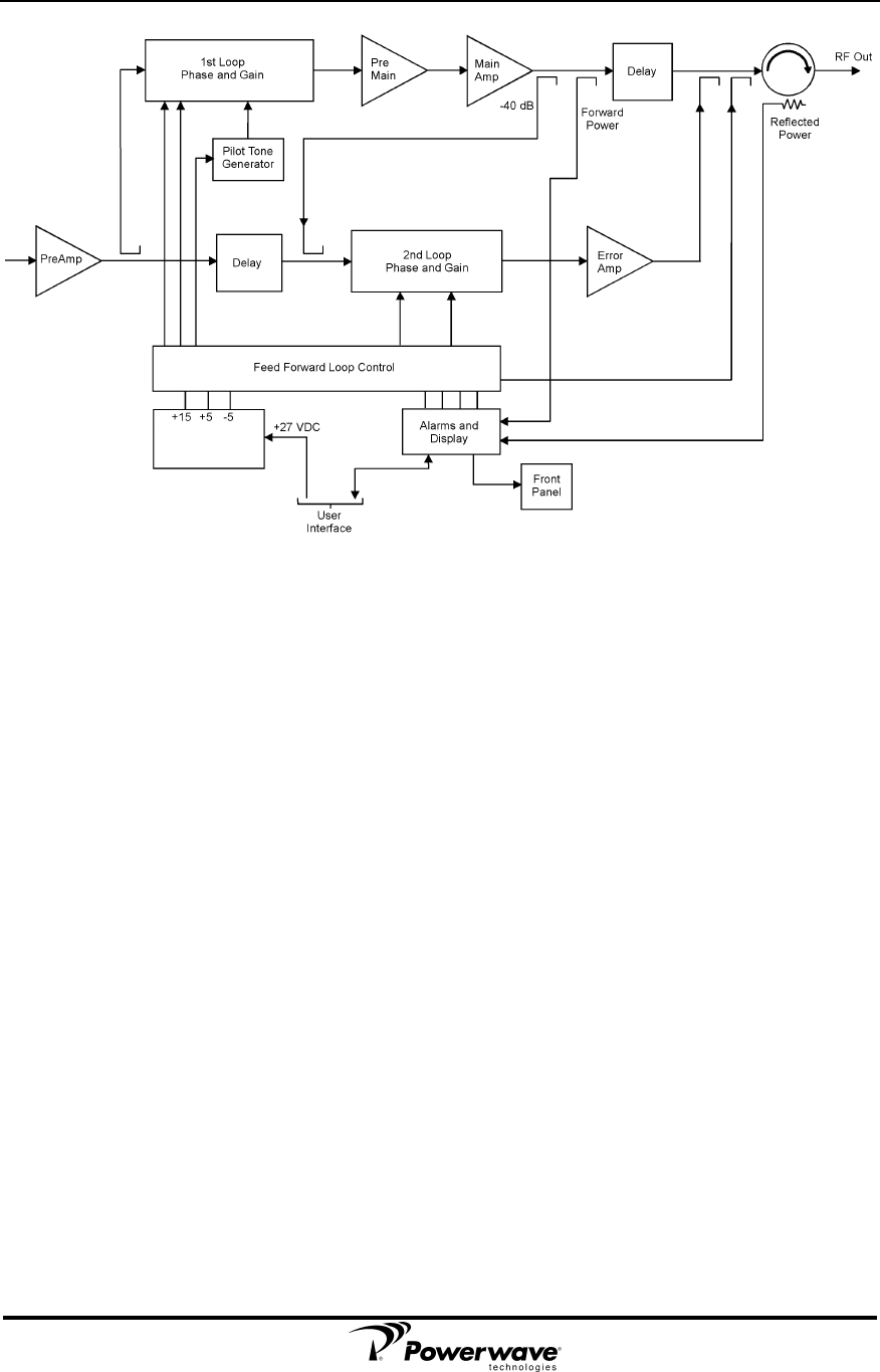
4-2 044-05177 Rev A
Figure 4-1. Functional Block Diagram
4-4.1 Preamplifier
The RF carriers are applied to the input port of the MCPA, where they are fed to the preamplifier
stage. The preamplifier provides two stages of class-A mode-amplification. The output of the
preamplifier is then split into two paths, one to the main amplifier and one to the error amplifier.
4-4.2 Main and Error Amplifiers
The main amplifier provides a balance of gain and power and employs class AB amplification for
maximum efficiency. The error amplifier and feed forward loops correct signal distortion
introduced by non-linearity in the class AB main amplifier. The error amplifier operates in class A
mode. The RF signal from the preamp is coupled to an attenuator and phase shifter in the first
feed-forward loop where it is phase shifted by 180 degrees and amplified in the pre-main
amplifier. The output from the pre-main amplifier is fed to the class AB main amplifier. The signal
output from the main amplifier is sampled using a coupler, and the sample signal is combined
with the main input signal and input to the second feed-forward loop.
The error signal is attenuated, phase shifted 180 degrees, then fed to the error amplifier where it
is amplified to a level identical to the sample output from the main amplifier. The output from the
error amplifier is then coupled back and added to the output from the main amplifier. The control
loops continuously make adjustments to cancel out any distortion in the final output signals.
4-4.3 Alarm Monitoring and Control
The alarm logic controls the +5 Vdc bias voltage that shuts down the amplifier. During routine
operation, all normal variations are automatically compensated for by the feed-forward loop
control. However, when large variations occur beyond the adjustment range of the loop control, a
loop fault occurs. When this happens, an alarm indicator is illuminated on the front panel of the
sub-rack. The fault is transmitted back to an external summary module via the external alarm
interface connection on the front panel of the sub-rack.

044-05177 Rev A 4-3
4-4.4 First and Second Loop Control Circuits
The primary function of the first loop is to amplify the carrier signals and isolate an error signal for
the second loop. The primary function of the second loop is to amplify the error signal to cancel
out spurious products developed in the main amplifier. The input signal is amplified by a
preamplifier and fed to a coupler and delay line. The signal from the coupler is fed to the
attenuator and phase shifter in the first loop. The first loop control section phase shifts the main
input signals by 180 degrees and constantly monitors the output for correct phase and gain.
The second loop control section obtains a sample of the distortion added to the output signals by
the main amplifiers. The signal is phase shifted 180 degrees, then fed to the error amplifier where
it is amplified to the same power level as the input sample. The signal is then coupled to the error
signal of the main amplifier output. The final output is monitored by the second loop and adjusted
to ensure that the signal distortion and intermodulation distortion (IMD) on the final output is
cancelled out.
4-4.5 Pilot Tone Generator
A pilot tone is an internally generated signal, who’s precise frequency, phase, and amplitude is
known. Passing through the amplifier, the pilot tone is distorted in the same way that signals are
distorted. To accomplish this, the pilot tone signal is injected into the first loop and then detected
at the feed-forward output of the second loop. The pilot tone is coupled off of the main amplifier,
thus creating a second pilot tone, attenuated and phase shifted 180 degrees to be used as the
reference. This second pilot tone is then amplified in the error amplifier and mixed with the
signals from the main signal path. Ideally, the two pilot tones, both amplified, should cancel each
other out. If they do not cancel each other out, as determined by an output detector, the
information is fed back to control the gain and phase of both the main and error amplifier paths
such that the output distortion is minimized.
4-5 Amplifier Module Cooling
The amplifier is cooled by forced air flowing over its heat sink, which is provided by external fans
mounted on the MCPA sub-rack. The fans are field replaceable. Each amplifier, when properly
cooled, maintains the amplifier within the specified operating temperature range. Six inches of
free space are required at both the front and rear panels of the sub-rack to allow adequate air
volume to circulate over the heat sinks.
4-6 Power Distribution
Primary DC power for the amplifier is provided by the host system. The amplifier module has a
DC/DC converter and voltage regulator that converts the +27 Vdc to +15 Vdc, +5 Vdc, and -5 Vdc
for internal use.

4-4 044-05177 Rev A
4-7 Amplifier Alarms
The amplifier alarms are listed and described in Table 4-1. The front panel LEDs are described in
Chapter 3.
Table 4-1. G3H-851-80 Alarm States
Major Alarm -
Causes MCPA RF section to be disabled Minor Alarm -
Does not cause MCPA RF section to be disabled
Amplifier
Alarm Definition Amplifier
Mode Auto-Recovery Event/Fault Log
Output
Overpower
Disable the MCPA
immediately if the output
power is > +2 dB over rated
power.
Major Input power decreases below
APC threshold (-11.2 dBm)
Records output
overpower event after
system disabled
Automatic
Power
Control
(APC)
Enabled if the output power
is > 51.7 dBm + 0.3 dB
Note: If the MCPA cannot
compensate the gain to
maintain compliance, the
Output Overpower or Input
Overdrive Faults will protect
the MCPA.
Minor
(Yellow LED
display)
Amplifier auto-recovers when
the output power drops below
51.6 + 0.3 dB.
Input
Overdrive
Disable the MCPA
immediately if the input RF
power is more than –5.7 dBm Major Input power decreases below
APC threshold (-11.2 dBm)
Records input overdrive
event, system disable
event, each auto
recovery event*
High
Temperature Sensor temperature is >
+85° C Major Amplifier auto-recovers when
the sensor temperature drops
to < +75° C.
Records over
temperature event,
system disable event,
each auto recovery
event,
Low Gain
Disable the MCPA if the gain
of the MPCA is lower than
+50 dB for a duration of 1
minute with input power no
more than 33 dBm
Major
(Blinking
yellow LED
display)
The amplifier attempts to
increase gain to more than +50
dB. After 10 unsuccessful
attempts, permanent shutdown.
Records low gain
event, system disable
event, each auto
recovery event,
Reflected
Power
Reverse RF output power is
> +48.3 dBm for a duration of
1-minute Major
MCPA waits 15 min before
initiating auto recovery.
Amplifier recovers if reverse
power is below +48.3 dBm
Records high reflected
power event, each auto
recovery event*
High
Voltage
Disable the MCPA
immediately if the supply DC
voltage > +30.5 Vdc Major Auto-recovery when the supply
voltage drops to < +29.5 Vdc
Records supply DC
fault event, system
disable event, each
auto recovery event*
Low
Voltage
Disable the MCPA
immediately if the supply DC
voltage < +20.5 Vdc Major Auto-recovery when the supply
voltage increases to > +24 Vdc
Records low voltage
event, system disable
event, each auto
recovery event*
Continued next page

044-05177 Rev A 4-5
Loop
Fail Loop convergence fail Major Loop converges. Tries to auto
recover 10 times before
permanent shut down.
Records internal DC
fault event, system
disable event, each
auto recovery event*
Internal
DC
Fail
Internal voltages failed or out
of range
Minor
(no LED
display)
Auto-recovery once the voltage
is within the range. After 10
attempts, if still unsuccessful,
permanent shutdown.
Records internal DC fail
event, system disable
event, each auto
recovery event*
Device
Fail One or more output power
devices fail
Major 10 auto-recovery attempts; if
still unsuccessful, permanent
shutdown..
Records device fault
event

4-6 044-05177 Rev A
(Page intentionally left blank)
044-05177 Rev A 5-1
Chapter 5
Maintenance
5-1 Introduction
This chapter contains periodic maintenance and performance test procedures for the
G3H-851-80 Multi-Carrier Power Amplifier (MCPA).
Note
Do not break the seals on equipment under warranty or the warranty will be null and
void. Do not return equipment for warranty or repair service until proper shipping
instructions are received from the factory.
5-2 Periodic Maintenance
Periodic maintenance requirements and the intervals at which the tasks should be performed are
listed in Table 5-1.
Table 5-1. Periodic Maintenance
Task Interval Action
Inspection:
Connectors
12 Months C
Ch
he
ec
ck
k
R
RF
F
c
co
on
nn
ne
ec
ct
to
or
rs
s
t
to
o
e
en
ns
su
ur
re
e
t
th
ha
at
t
t
th
he
ey
y
a
ar
re
e
t
ti
ig
gh
ht
t.
.
P
Pe
er
rf
fo
or
rm
ma
an
nc
ce
e
T
Te
es
st
ts
s 12 Months P
Pe
er
rf
fo
or
rm
m
a
an
nn
nu
ua
al
l
t
te
es
st
t
p
pe
er
r
p
pa
ar
ra
ag
gr
ra
ap
ph
h
5
5-
-4
4.
.
C
Cl
le
ea
an
n
F
Fa
an
ns
s/
/H
He
ea
at
t
S
Si
in
nk
ks
s 3 Months I
In
ns
sp
pe
ec
ct
t
f
fo
or
r
d
de
eb
br
ri
is
s.
.
R
Re
em
mo
ov
ve
e
d
du
us
st
t
w
wi
it
th
h
a
a
s
so
of
ft
t
c
cl
lo
ot
th
h/
/b
br
ru
us
sh
h
o
or
r
v
va
ac
cu
uu
um
m
c
cl
le
ea
an
ne
er
r.
.
C
Cl
le
ea
an
n
t
th
he
e
f
fa
an
n
b
bl
la
ad
de
es
s
i
in
n
t
th
he
e
a
as
ss
so
oc
ci
ia
at
te
ed
d
s
su
ub
b-
-
r
ra
ac
ck
k.
.
5-3 Test Equipment Required For Test
Test equipment required to test the amplifier is listed in Table 5-2. Equivalent test equipment may
be substituted for any item, keeping in mind that a thermistor type power meter is required.
Note All RF test equipment required must be calibrated to 0.05 dB resolutions. Any
deviation from the nominal attenuation must be accounted for and factored into
all output readings.
Table 5-2. Test Equipment Required
Nomenclature Manufacturer Model
5-2 044-05177 Rev A
Signal Generator Agilent 8656B
20 dB Attenuator, 250 Watt Bird
20 dB Attenuator, 20 Watt (2 each) Bird Tenuline
Spectrum Analyzer Agilent 8560E
Coax Directional Coupler Agilent 778D
Power Meter / Sensor Agilent 437B / 8481A
Arbitrary Waveform Generator Sony AWG2021
Network Analyzer Agilent 8753C
* Any equipment substituted should have equivalent specifications.
5-4 Amplifier Performance Test
Performance testing should be conducted every 12 months to ensure that the amplifier system
meets the operational specifications listed in Table 5-3. Also verify system performance after any
amplifier module is replaced in the field.
The test equipment required to perform the testing is listed in Table 5-2, and the test setup is
shown in Figure 5-1 and Figure 5-2.
Note
The frequencies used in this test are typical for an amplifier with a 18 MHz band from
851 MHz to 869 MHz. Select evenly spaced F1, F2, F3, and F4 frequencies that
cover the instantaneous bandwidth of your system.
To check amplifier performance, proceed as follows:
WARNING Do not apply any RF signals to the amplifier input until instructed to do
so.
CAUTION
Ensure that the correct amount of attenuation is used between the amplifier RF
connections and the test equipment to prevent overdrive of the amplifier or the
test equipment.
5-4.1 Amplifier Spurious Emissions Test:
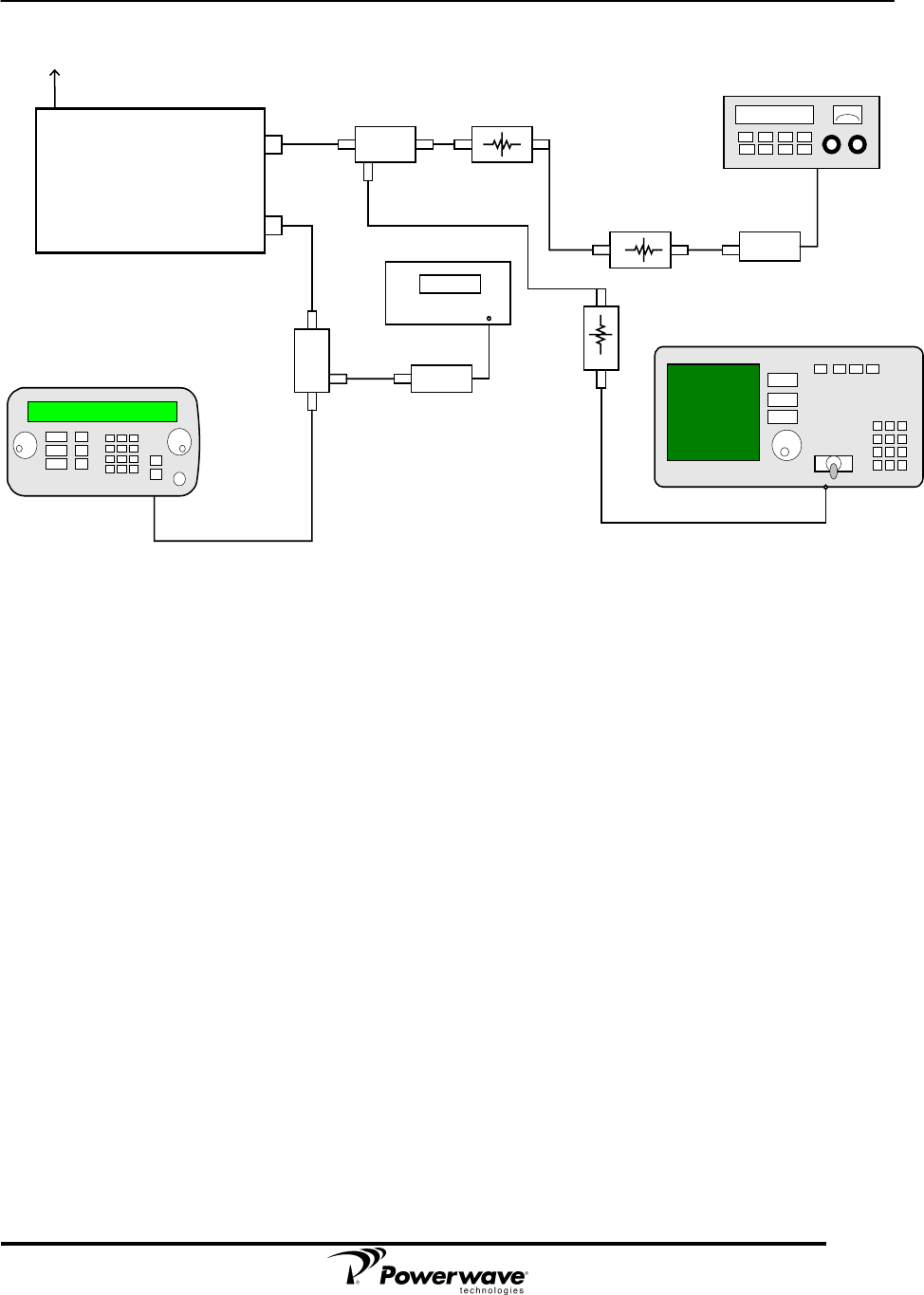
1. Connect the test equipment as shown in Figure 5-1.
2. Configure the signal source to produce four frequencies evenly spaced across the
instantaneous bandwidth to be used for the amplifier under test.
3. Adjust the output of the signal source to excite the amplifier to its rated output.
4. Use the spectrum analyzer to measure the spurious emissions performance.
5. Record test data in Table 5-3. Verify that the data are within the specifications shown in
Table 1-1.
6. Reduce the output of the signal source to minimum.
7. Switch off the Main Power Switch on the amplifier under test.
044-05177 Rev A 5-3
G3H-851-80 PYTHON Multi-
Channel Power Amplifier
Gain = 63 dB
Output = 80 W = +49.03 dBm
27 Vdc
RF Out
RF In
20 dB
Directional
Coupler 30 dB
Attn
250 W
High Pwr
04-0262B-A
Sensor
Head 8482A
30 dB
Attn
20 W
20 dB
Directional
Coupler
Sensor
Head 8482A
Power Meter
INPUT
HP 8560 E
+1.3
dBm*
* Example. Ensure that sufficient
attenuation is present between the
amplifier output and your test equipment
to avoid overdrive or damage. Refer to
test equipment specifications.
Spectrum
Analyzer
HP 8648 A
HP 437B
Signal
Source
Power
Meter
TEST
CONFIGURATION
A
20 dB
Attn
Figure 5-1. Amplifier Test Setup Diagram – Configuration A
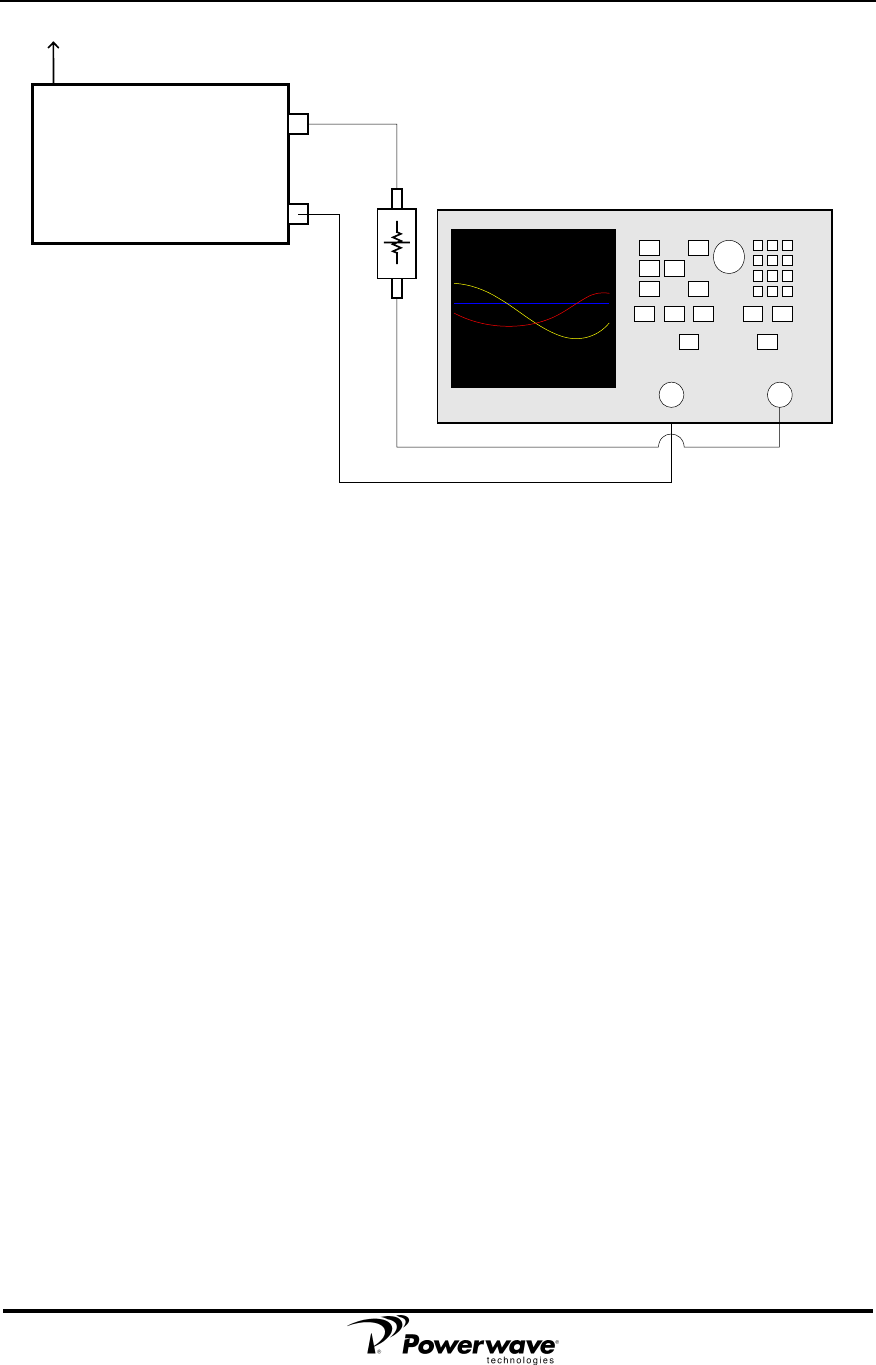
5-4.2 Gain Test:
1. Disconnect:
a. Spectrum analyzer
b. Signal source.
c. Power Meter and Sensor Head.
2. Connect the network analyzer as shown in Figure 5-2.
3. Set network analyzer as follows:
a. Power output to -11 dBm max.
b. Frequency start to 851 MHz.
c. Frequency stop to 869 MHz.
d. Normalize the network analyzer for gain and return loss.
4. Switch on the amplifier under test, and ensure that the STATUS switch is in the center
position.
5. Check the amplifier gain across the band from 851 MHz to 869 MHz. Gain should be as
specified in Table 1-1. Record test data in Table 5-3.
5-4 044-05177 Rev A
G3H-851-80 PYTHON Multi-
Channel Power Amplifier
Gain = 63 dB
Output = 80 W = +49.03 dBm
27 Vdc
RF Out
RF In
40 dB
Attn
250 W
+1.3
dBm*
* Example. Ensure that sufficient
attenuation is present between the
amplifier output and your test
equipment to avoid overdrive or
damage. Refer to test equipment
specifications.
Network
Analyzer
TEST
CONFIGURATION
B
04-0263B-A
PORT 1
HP 8753 D
PORT 2
Figure 5-2. Amplifier Test Setup – Configuration B
5-4.3 Input Return Loss:
1. Retain the test configuration shown in Figure 5-2.
2. Read and record the S11 return loss measurement on network analyzer. Record test data in
Table 5-3.
3. Switch off the amplifier under test.
4. Disconnect the test equipment.

044-05177 Rev A 5-5
5-4.4 Test Data Sheet
Record the amplifier’s performance test data below.
DATE MODULE S/N
Test Conditions:
Load and Source Impedance: 50 Ohms
VSWR: < 1.5:1
Supply Voltage: +27 Vdc ±0.1 Vdc
Table 5-3. Amplifier Performance Data
Test Specification Min Max Data
RF Gain Vcc = 27 Vdc
PO = See Table 1-1
Freq. = 851 – 869 MHz
62.5 dB 63.5 dB
Spurious
Emissions
Vcc = 27 Vdc
PO = See Table 1-1
851 – 869 MHz Band
-63 dBc
Gain Flatness Vcc = 27 Vdc
PO = See Table 1-1
851 – 869 MHz Band
±0.5 dB
Input Return
Loss
Vcc = 27 Vdc
PO = See Table 1-1
851 – 869 MHz Band
-
-1
16
6
d
dB
B
PASS FAIL
Tested by
5-5 Return For Service Procedures
When returning products to Powerwave, the following procedures will ensure optimum response.
5-5.1 Obtaining An RMA
A Return Material Authorization (RMA) number must be obtained prior to returning equipment to
the factory for service. Please contact our Repair Department at (714) 466-1000 to obtain this
number, or FAX your request to (714) 466-5800. Failure to obtain this RMA number may result in
delays in receiving repair service.
5-5.2 Repackaging For Shipment
To ensure safe shipment of the amplifier, it is recommended that the original package designed
for shipping the amplifier be reused. If it is not available, contact Powerwave’s Customer Service
Department for packing materials.

5-6 044-05177 Rev A
(Page intentionally left blank)

044-05177 Rev A A-1
Appendix A
Abbreviations and Acronyms
Below is a list of the abbreviations and acronyms used in the industry.
Abbreviation/
Acronym Definition
ACLR Adjacent Channel Leakage Power Ratio
ACP Adjacent Channel Power
A/D Analog-to-Digital Conversion
ADC {Analog-to-Digital Converter
{Automatic Data Collection
AM Amplitude Modulation
AMPS Advanced Mobile Phone System
ANSI American National Standards Institute
APC Automatic Power Control
APTT Analog Push To Talk
ASG Applications Support Group
ASIC Application Specific Integrated Circuit
ATE Automatic (Automated) Test Equipment
ATP Acceptance Test Procedure
ATTEN Attenuator
BER Beyond Economical Repair
BOM Bill Of Materials
BPF Band Pass Filter
BS Base Station
BTS Base Transceiver Station (System)
BW BandWidth
°CDegrees Celsius
CAD Computer Aided Design
CCA {Circuit Card Assembly
CCW Counter ClockWise
CDMA Code Division Multiple Access
CDPD Cellular Digital Packet Data
CTRL Control
CW {ClockWise
{Continuous Wave

A-2 044-05177 Rev A
Abbreviation/
Acronym Definition
dB deciBels
dBc Referenced to a carrier level
dBm Reference to one milliwatt
dBw Reference to one watt
DIN Deutsches Insitut für Normung eV
DLNA Duplexer Low Noise Amplifier
DPTT Digital Push To Talk
DQPSK Differential Quadrature Phase Shift Keyed
DSP Digital Signal Processing
DUT Device Under Test
ECD Estimated Completion Date
ECM Electronic Counter Measure
EDGE Enhanced Data for GSM Evolution
EEPROM Electrically-Erasable Programmable Read-Only Memory
EIA Electronic Industries Association
EMC ElectroMagnetic Compatibility
EMI ElectroMagnetic Interference
EPROM {Electrically Programmable Read-Only Memory
{Erasable Programmable Read-Only Memory
ESD ElectroStatic Discharge
ESG Electronic Signal Generator
ETDMA Extended Time Division Multiple Access
ETSI European Telecommunications Standard Institute
EUT Equipment Under Test
FAR Failure Analysis Report
FCC Federal Communications Commission
FDMA Frequency Division Multiple Access
FET Field Effect Transistor
FHMA Frequency Hopping Multiple Access
FM Frequency Modulation
FRU Field Replaceable Unit
FSK Frequency Shift Key modulation
GHz Gigahertz
GMSK Gaussian Minimum Shift Keying
GOLAY See GSC
GSC Golay Sequential Code

044-05177 Rev A A-3
Abbreviation/
Acronym Definition
GSM Global System for Mobile Communications
HPF High Pass Filter
HW Hardware
Hz Hertz
IAW In Accordance With
IC Integrated Circuit
IMD InterModulation Distortion
IRL Input Return Loss
IS-54 Interim Standard 54 for TDMA
IS-95 Interim Standard 95 for CDMA
ISDN Integrated Services Digital Network
ISM Industrial, Scientific and Medical unlicensed frequency bands
ISO {International Organization for Standardization
{ISOlator
kHz Kilohertz
LDA Linear Discrete Amplifier (Class A or AB)
LGL Lower Guardband Limit
LMR Land Mobile Radio
LMS Land Mobile Systems
LNA Low Noise Amplifier
LO Local Oscillator
LPA Linear Power Amplifier
LPF Low Pass Filter
LSL Lower Specification Limit
LVD Low Voltage Disconnect
MC MultiChannel
MCA MultiChannel Amplifier
MCPA {MultiCarrier Power Amplifier
{MultiChannel Power Amplifier
MCR MultiChannel Rack
MFRM {Multiple Frequency Radio Mobile
{Multifunction Frequency Radio Modulation
MHz Megahertz
MSO Master Switch Office
MTBF Mean Time Between Failures
MTSO Master Telephone Switch Office

A-4 044-05177 Rev A
Abbreviation/
Acronym Definition
MU Measurement Uncertainty
M&TE Measuring and Test Equipment
NAMPS Narrow Analog Mobile Phone System
NIOSH National Institute for Occupational Safety and Health
NIST National Institute for Standards and Technology
NMT Nordic Mobile Telephone
NVM NonVolatile Memory
OEM Original Equipment Manufacturer
OFDM Orthogonal Frequency Division Multiplexing
OMS Operational Method Sheet
OOB Out Of Box
O/P Output
OSHA Occupational Safety and Health Administration
PA Power Amplifier
PAF Powerwave Amplifier Frame
PAR Peak to Average Ration
PCB Printed Circuit Board
PCMCIA Personal Computer Memory Card International Association
PCN Personal Communications Network
PCS {Personal Communications Services
{Personal Communication System(s)
PDA Personal Digital Assistant
PEP Peak Envelope Power
PF PicoFarads
PHS Personal Handyphone System – Japan
PLC Product Life Cycle
PLL Phase Locked Loop
PM {Phase Modulation
{Preventive Maintenance
PMR Peak to Minimum Ratio
PO Purchase Order
PPM Parts Per Million
PSC {PCS Single Channel
{Product Serialization Code
PSTN Public Switched Telephone Network
PTI Powerwave Technologies, Inc.

044-05177 Rev A A-5
Abbreviation/
Acronym Definition
PTT Push To Talk
PWAV Powerwave
QA Quality Assurance
QAM Quadrature Amplitude Modulation
RBW Resolution Band Width
RF Radio Frequency
RFI Radio Frequency Interference
RFQ Request For Quotation
RFS RF Solutions
RFSU RF Switching Unit
RGO Return Goods Order
RH Relative Humidity
RL Return Loss
RMA {Rack-Mounted Amplifier
{Return Material Authorization
RMP Reliability Monitoring Plan (Procedure)
RMS Root Mean Square
RSS Root Sum Square
Rx Receive, Receiver
SCHPA Single-Channel High Power Amplifier
SCPA Single Channel Power Amplifier
SIM System Interface Module
SMA SubMiniature Type A (coaxial connector)
SMT Surface Mount Technology
SN Serial Number
SO System Outage
SOE Sequence of Events
SW SoftWare
TBC To Be Confirmed
TBD To Be Determined (To Be Defined)
TCXO Temperature Controlled crystal Oscillator
TD {Temperature Drift
{Temporary Deviation
TDMA Time Division Multiple Access
TRU Transmit Receive Unit

A-6 044-05177 Rev A
Abbreviation/
Acronym Definition
TRX Transceiver (Transmit / Receiver) Unit
Tx Transmit, Transmitter
UAI Use As Is
UART Universal Asynchronous Receiver Transmitter
UCL Upper Control Limit
UCLR Upper Control Limit for Range
UGL Upper Guardband Limit
UL Underwriters Laboratories
UMTS Universal Mobile Telecommunications System
UNL Unit Nominal Level
URG Unit Reference Gain
USL Upper Specification Limit
UUT Unit Under Test
VADJ Voltage ADJust (signal name frequently found on schematic or block
diagrams)
VBW Video Band Width
VCO Voltage Controlled Oscillator
VFWD Voltage ForWarD (signal name frequently found on schematic or block
diagrams)
VREFL Voltage REFLected (signal name frequently found on schematic or block
diagrams)
VSWR Voltage Standing Wave Ratio
VVA Voltage Variable Attenuator
WCDMA Wideband Code Division Multiple Access
XMT Transmit
XMTR Transmitter

NOTES

Corporate Headquarters
Powerwave Technologies, Inc.
1801 East St. Andrew Place
Santa Ana, CA 92705 USA
Tel: 714-466-1000
Fax: 714-466-5800
www.powerwave.com
©Copyright January 2005, Powerwave Technologies, Inc. All Rights reserved. Powerwave, Powerwave Technologies, The Power in Wireless and the Powerwave logo are registered trademarks of Powerwave Technologies, Inc.
Main European Office
Antennvägen 6
SE-187 80 Täby
Sweden
Tel: +46 8 540 822 00
Fax: +46 8 540 823 40
Hong Kong Office
23 F Tai Yau Building
181 Johnston Road
Wanchai, Hong Kong
Tel: +852 2512 6123
Fax: +852 2575 4860