Powerwave Technologies BDA1200 Bi-Directional Amplifier, Model BDA1200 User Manual Alig

Powerwave Technologies Inc. Bi-Directional Amplifier, Model BDA1200 Alig

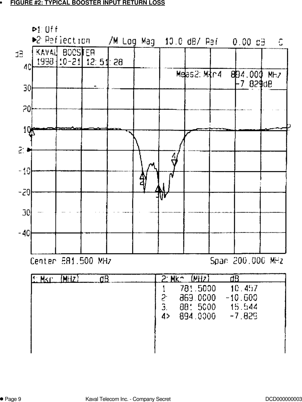
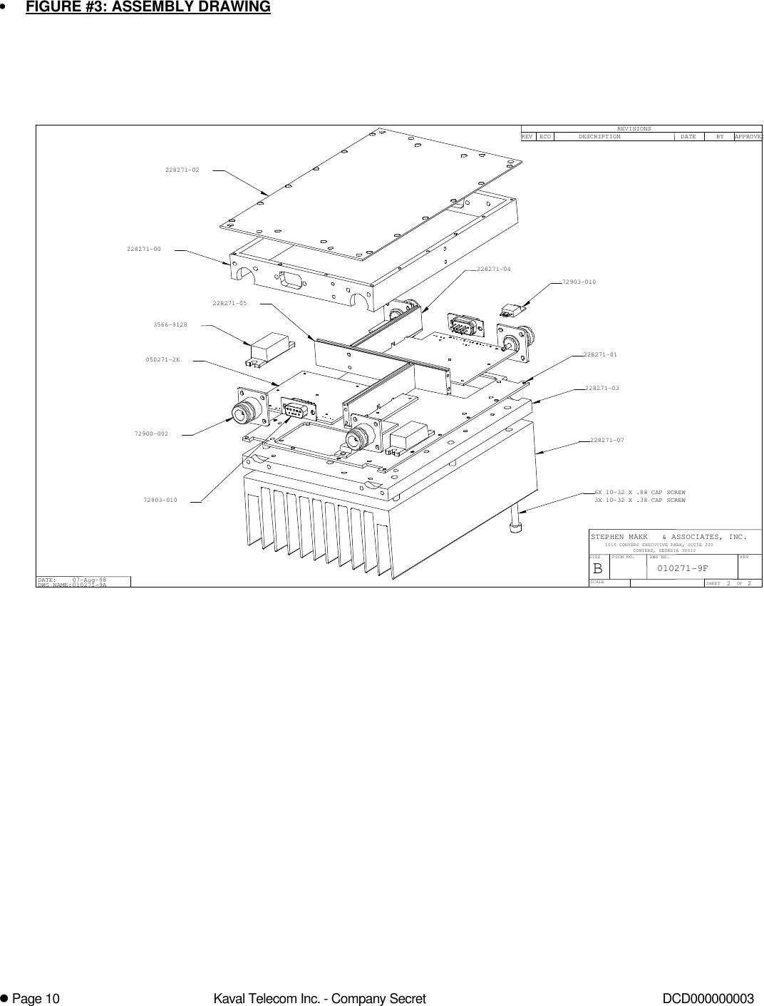
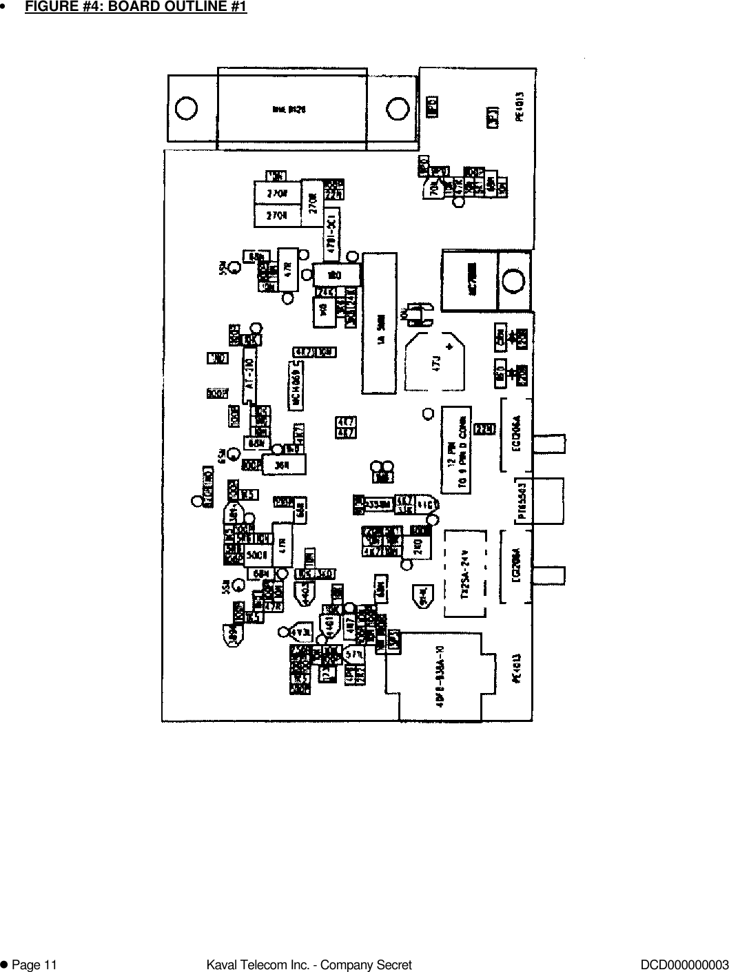
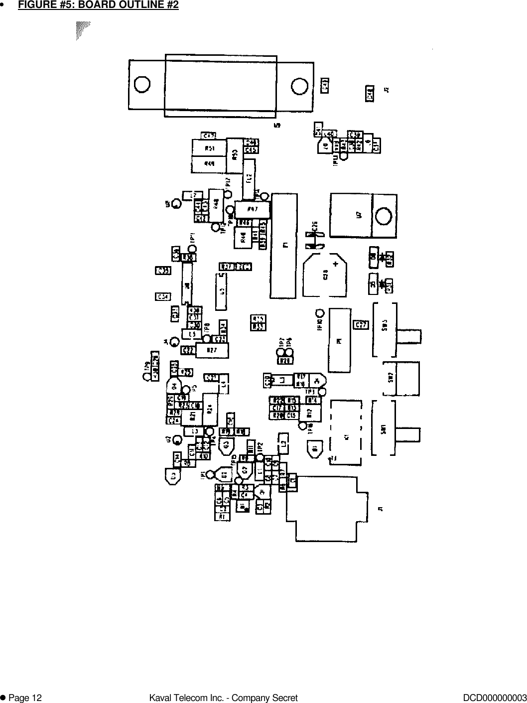
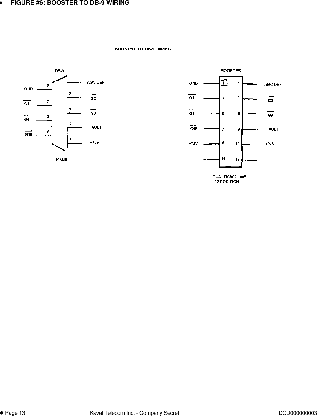
Test and alignment spec for booster

l Page 1Kaval Telecom Inc. - Company Secret DCT00000000360 GOUGH ROAD, MARKHAM, ONTARIO L3R 8X7Tel: (905) 940-1400 Toll Free: 888-86KAVAL Fax: (905) 946-3392TEST & ALIGNMENT SPECIFICATIONFOR BDA 800 MHz 1W BoosterDCT000000003Revision 1, May 18, 1999TITLE SIGNATURE DATEOriginatorProduct Group Team LeaderMarketingAdministration
l Page 2Kaval Telecom Inc. - Company Secret DCD000000003TABLE OF CONTENTS•REVISION RECORD 3•PROPRIETARY NOTICE: 3•INTRODUCTION: 4•EQUIPMENT 4•MATERIALS 4•DOCUMENTATION 4•PROCESS 5•Inspection and Preparation 5•Housing Kit. 5•PCB 5•Divider Wall Subassembly 5•Hookup Wire. 5•Regulator Leads 5•Installation of Leaded Components 5•Installation of PCB into Housing 5•Installation of Bolted Components 5•Installation of Divider Wall Assembly 5•BIAS TEST 6•ALIGNMENT OF FAULT DETECT 6•RF TEST 6•Swept Response 6•Overall Gain 6•Passband 6•Input Return Loss 6•Single Tone Tests 6•Saturated Power 6•Coarse Gain Adjustment 6•Maximum Gain 6•AGC Alignment 7•Verification of Fine Gain Control 7•INSTALLATION OF BOTTOM COVER 7•FINAL TEST AND INSPECTION 7•FIGURE #1: TYPICAL BOOSTER RESPONSE WITH LID REMOVED 8•FIGURE #2: TYPICAL BOOSTER INPUT RETURN LOSS 9•FIGURE #3: ASSEMBLY DRAWING 10•FIGURE #4: BOARD OUTLINE #1 11•FIGURE #5: BOARD OUTLINE #2 12•FIGURE #6: BOOSTER TO DB-9 WIRING 13
l Page 3Kaval Telecom Inc. - Company Secret DCD000000003• REVISION RECORDRevisions are tracked here as ...1May 18, 1999 Updated from SMA Documents Alan Aslett• PROPRIETARY NOTICE:This document contains restricted, proprietary, copyrighted information, ownership of which is retained by Kaval Telecom Inc.   Kaval Telecom Inc.’s express written consent is required prior to any  reproduction, implementation, publication or other use ofsuch information. This is a controlled document for internal company use only, and is to be distributed only to the parties listedin the Distribution List.  Technical information in this document may qualify for patent protection, and for this reason, “publicdisclosure”, as defined in applicable Patent Law is strictly forbidden except with the express written authorization of thePresident of Kaval Telecom Inc.This document is considered “Strategic Technical Information” by Kaval Telecom Inc.   All Kaval employee recipients mustmaintain confidentiality in accordance with Kaval Employee Confidentiality regulations per the Employee Manual.All contractors in possession of this information must maintain confidentiality in accordance with applicable Non-DisclosureAgreements and Product Development Agreements, but notwithstanding the preceding, shall, at a minimum, maintain at leastthe same level of confidentiality that they apply to their own confidential internal documents.
l Page 4Kaval Telecom Inc. - Company Secret DCD000000003• INTRODUCTION:This document provides a step by step procedure for final assembly and test of a Kaval dual cellular booster.   Thisprocedure presupposes availability of a complete mechanical parts kit and PCBs with all SMD parts installed. Majoractivities are installation of PCBs into housing, installation of remaining parts and test. Because of the nature of theinterface connector, it is easier to test PCBs once installed.  There are no parts on the underside of the PCB, so all repairscan be done without removing PCBs from housing.  This procedure is specific to the production of cellular band boostersintended for installation into Cellcom BDA systems.  Some adjustment parameters may differ for other customers andapplications. It is recommended that debug and repair not be done by personnel that do test.   Unit should be taken to anoffline repair station.   Test operator should apply a tag or sticker to defective unit coded with paragraph number of teststep at which unit failed.  It is recommended that a test checklist be produced to accompany this document which is used torecord test results for each unit.   Checklist should refer to paragraph numbers of tests.   This can have plots attached andshould be filed by serial number for future reference.• EQUIPMENTThe following tools or instruments are required for final assembly:MultimeterBooster test interface (custom made)24V DC Power supply with current limiting at 1AScalar Network Analyzer capable of 900 MHz operation1W minimum 10 or 20 dB attenuator, type N.Type N test cablesN- Female to N-Female adapter.1 Ohm 1W Resistor with test leads.  (One banana, the other, a pointed probe such as used with multimeters)Insulated Tuning Screwdriver#0 Philips Screwdriver#1 Philips Screwdriver (preferably motorized)Nutdriver for D-sub jack screws.Wire StripperFlush CutterStatic Protected Soldering StationHobby KnifeModerate Viscosity Cyanoacrylate GlueCoarse File or Dremel Tool• MATERIALSEach Dual Booster requires the following materials.   Refer to BOM for details.2 Booster PCB Assemblies1 Housing Kit.Approx. 13.5” #24 AWG insulated hookup wire, assorted colours.Heatsink GreaseParts listed on BOMs• DOCUMENTATIONReferenced documentation is listed below:DCA000000001:  Assembly Drawing, 1W Dual BoosterSCH000000004: Schematic Diagram: 800MHz 1W Booster
l Page 5Kaval Telecom Inc. - Company Secret DCD000000003• PROCESS• Inspection and Preparation• Housing Kit.Inspect housing parts for hazardous burrs, loose metal chips and clean and deburr as required.   If machiningoil residue exists, clean with Varsol.Install Top Cover to Wall Extrusion using 16 #2-56 flat head machine screws.• PCBInspect PCB for missing or improperly installed SMD parts.Using a file or Dremel tool, chamfer two corners of PCB closest to RF connectors approximately 0.100” toeliminate interference with weld fillets in housing.• Divider Wall SubassemblyInstall two divider walls to center divider wall using 4 #2-56 x 3/8” thread cutting screws.   Be mindful ofcorrect orientation of grooves and notched in walls to ensure they conform to PCB ground locations and allowclearance for components.Install EMI gasket material to grooves in underside of divider wall assembly.    Cut gasket to length so that itis only installed where divider wall meets exposed ground on top of PCB or where divider walls contact metalhousing.   Be careful that stray embedded wires do not possibly contact any active traces on PCB.  Gasketbits should be tack-glued to divider assembly with sparing use of cyanoacrylate glue.   (Loctite type 401recommended).• Hookup Wire.Cut hookup wire to 1.5” length.   Use different colour wires for each connection (resistor color codingcorresponding to pin number on D connector is recommended)Strip one end (PCB) to a length of 0.080”, other end (D-connector) to 0.150”.• Regulator LeadsTrim voltage regulator leads to a length of 0.200”• Installation of Leaded ComponentsInstall fuse clips into PCB.    It may be helpful to install a fuse into the clips before clip insertion into PCB to assurecorrect alignment.Install hookup wires to location P1.   Refer to Interconnect Diagram for connection details.Using flush cutters, trim fuse clip and wire leads flush with PCB.    Length of protrusion below PCB cannot exceed0.030” or short circuits may occur.• Installation of PCB into HousingInstall PCB assemblies into housing.   8 pcs #4-40 x 5/16” thread forming screws are used to fasten down eachbooster PCB.   Screws go through top plate and into heatsink.   Note that one screw hole in PCB is not used.   This isnormal.Be sure that one PCB of each band split is installed.   One should have an 881 MHz dielectric filter (F1), the othermust be an 836 MHz part.• Installation of Bolted ComponentsApply heatsink grease (a.k.a. Synthetic Gorilla Snot) to regulator and power module tabs.Note: Be sure to stir compound thoroughly before using.   Apply a minimal amount.  Excess compound actuallyreduces thermal conductivity.  Objective is to eliminate air voids between device tab and heatsink.   Avoid getting thismaterial on clothing.   There is no known way of removing it from fabrics.Install voltage regulators and RF power modules to heatsink using 6 pcs. #6-32 x 5/16 thread forming screws.Solder all connections of installed parts just installed.Install filtered 9 pin D connector from outside of housing.     Fasten it down using two hex jack screws with singlelockwashers (252900-00).  Note: Jack screw kits will have excess parts that are unused.Solder interconnect wires to D connector in accordance with sketch.• Installation of Divider Wall AssemblyInstall divider wall assembly into housing and fasten with 8 pcs #2-56 x 3/8 thread cutting screws.   It is helpful toclamp divider assembly down with a clamp or toggle press to ensure gaskets are compressed and holes line up.Inspect divider wall areas of PCB to ensure no components short to wall.   Realign components as needed.NOTE:   This step can be done after bias test if divider walls are not available, but these steps must be repeatedafter wall installation in such case.
l Page 6Kaval Telecom Inc. - Company Secret DCD000000003• BIAS TESTThis test is performed for each booster PCB.   A multimeter is used for all voltage measurements.  All measurementsare with respect to chassis ground, so connect multimeter negative lead to any convenient point on metallic housingusing an alligator clip.Plug test adapter module into 9 pin connector.Set a laboratory power supply to 24 VDC +/- 0.1 VDC and current limit it to 0.75A.Connect PSU to banana jacks on test adapter.Set AGC switch to off position and coarse gain to on position.Apply power.   Verify PSU does not current limit.   Verify supply current draw is 600 mA +/- 50 mAVerify voltage at TP 10 is +24 VDC +/- 0.1VVerify voltage at TP 14 is +23.85 VDC +/- 0.1V.Verify voltage at TP18 is 23.5 VDC +/- 0.15 VVerify voltage at pin 3 of U9 is 12 VDC +/- 0.25 VVerify Voltage at TP12 is 8 VDC +/- 0.25 VVerify voltage at TP1 is 4.4 VDC +/- 0.2 VVerify voltage at TP2 is 5.0 VDC +/- 0.25 VVerify voltage at TP4 is 5.0 VDC +/- 0.25 VVerify voltage at TP5 is 2.8 VDC +/- 0.25 VVerify voltage at TP9 is < 0.3 VDCVerify voltage at TP15 is < 0.3 VDCSwitch Coarse Gain off.Verify voltage at TP4 is < 0.3 VDCVerify voltage at TP5 is < 0.3 VDCVerify voltage at TP9 is 3.8 VDC +/- 0.25 VDCVerify voltage at TP8 is 5.5 VDC +/- 0.25 VDCVerify voltage at TP11 is 8.0 VDC +/- 0.25 VVerify voltage at TP17 is 5.0 VDC +/- 0.25 VDC• ALIGNMENT OF FAULT DETECTConnect a 1W 1 Ohm resistor between TP14 and TP18.  This simulates a reduction of power module current by 50%.Adjust R40 so that fault light on test adapter turns off.Carefully adjust R40 so that fault light barely turns on.Remove 1W resistor.   Verify fault light goes out.• RF TEST• Swept Response• Overall GainConnect unit to scalar network analyzer or spectrum analyzer with tracking generator.   Set input level to –50dBm.   Sweep center frequency +/- 100 MHz.   Set AGC off, coarse gain off fine gain to maximum.   Verifymidband gain is 54 dB +/- 2 dB.   See Fig. 1 for sample plot.  Note: Plot shows booster at full gain.   Shapeshould be the same at lower gains.• PassbandVerify gain within operating passband does not vary from reading in 6.8.2 by more than +/- 1 dB.Verify rejection at offsets of +/- 100 MHz is at least 35 dB.• Input Return LossSet coarse gain to on.   Verify input return loss over operating passband is greater than 10 dB.   See Fig. 2 forsample plot.• Single Tone Tests• Saturated PowerApply a single tone at input at a level of –30 dBm at the center of the application operating band.    Verifyoutput power is at least +30 dBm.• Coarse Gain AdjustmentSet coarse gain off.   With input signal at a level of –50 dBm, measure output level.   Set coarse gain on.Adjust R21 to obtain an output level of 16 dB +/- 0.25 dB higher than reading obtained with coarse gain off.• Maximum GainCalculate difference between output level and – 50 dBm.   This is the maximum gain.    Verify this to be +70dB +/- 2 dB.
l Page 7Kaval Telecom Inc. - Company Secret DCD000000003• AGC AlignmentWith an input signal level of – 30 dBm, with coarse gain on, fine gain at max and AGC on, adjust R12 to obtain an outputlevel in accordance with the table below.   Settings are derived using FCC recommended procedure for determiningchannel loading of multichannel amplifiers.APPLICATION AGC Single Carrier Target LevelStandalone Booster +20 dBmBooster used with SMA 20W Amplifier +15 dBmBooster used with TRL 35W Amp with +51dBm IP3 +10.5Booster used with TRL 35W amp that conforms to +55.5dBm IP3 +15 dBm• Verification of Fine Gain ControlWith a single carrier input level of –50 dBm, AGC off and all gains set to max, observe the output level while decreasing fine gainstep by step.    Verify that steps are monotonic and that with fine gain set to minimum, overall gain is less than maximum gain by 16dB +/- 0.7 dB.   (Monotonic means that the steps are in the right order, that when you reduce gain by any 1 dB step, the gainchange is in the right direction.   Some attenuator faults may result in steps getting out of order when you cross a high bitboundary.)• INSTALLATION OF BOTTOM COVERInstall labels (uplink/downlink) near 9 pin connectors.   Ensure labels go with correct PCB boards.Install bottom cover (to assembly using 16 #2-56 flat head screws.• FINAL TEST AND INSPECTIONIf required by customer contract, repeat swept measurement at full gain to produce a final plot for shipment to customer orfor file.   This also verifies that cover installation did not disrupt the circuitry as gaskets were compressed.Inspect housing for missing screws.Affix nameplate with serial number.Pack unit for shipment if applicable.
l Page 8Kaval Telecom Inc. - Company Secret DCD000000003• FIGURE #1: TYPICAL BOOSTER RESPONSE WITH LID REMOVED
l Page 9Kaval Telecom Inc. - Company Secret DCD000000003• FIGURE #2: TYPICAL BOOSTER INPUT RETURN LOSS
l Page 10 Kaval Telecom Inc. - Company Secret DCD000000003• FIGURE #3: ASSEMBLY DRAWING3X 10-32 X .38 CAP SCREW6X 10-32 X .88 CAP SCREW72903-01072900-00272903-010228271-01228271-03228271-07228271-04228271-05050271-2E3566-9128228271-00228271-02010271-9F22010271-9ADWG NAME:07-Aug-98DATE:CONYERS, GEORGIA 300121015 CONYERS EXECUTIVE PARK, SUITE 200& ASSOCIATES, INC.STEPHEN MAKK  OFAPPROVEDBYDATEREVISIONSECOREVDESCRIPTIONBREVFSCM NO.DWG NO.SHEETSCALESIZE
l Page 11 Kaval Telecom Inc. - Company Secret DCD000000003• FIGURE #4: BOARD OUTLINE #1
l Page 12 Kaval Telecom Inc. - Company Secret DCD000000003• FIGURE #5: BOARD OUTLINE #2
l Page 13 Kaval Telecom Inc. - Company Secret DCD000000003• FIGURE #6: BOOSTER TO DB-9 WIRING

Navigation menu