Powerwave Technologies BDA1200 Bi-Directional Amplifier, Model BDA1200 User Manual Alig
Powerwave Technologies Inc. Bi-Directional Amplifier, Model BDA1200 Alig
Contents
test and alignment for booster

l Page 1Kaval Telecom Inc. - Company Secret DCT000000003
60 GOUGH ROAD, MARKHAM, ONTARIO L3R 8X7
Tel: (905) 940-1400 Toll Free: 888-86KAVAL Fax: (905) 946-3392
TEST & ALIGNMENT SPECIFICATION
FOR BDA 800 MHz 1W Booster
DCT000000003
Revision 1, May 18, 1999
TITLE SIGNATURE DATE
Originator
Product Group Team Leader
Marketing
Administration
l Page 2Kaval Telecom Inc. - Company Secret DCD000000003
TABLE OF CONTENTS
•REVISION RECORD 3
•PROPRIETARY NOTICE: 3
•INTRODUCTION: 4
•EQUIPMENT 4
•MATERIALS 4
•DOCUMENTATION 4
•PROCESS 5
•Inspection and Preparation 5
•Housing Kit. 5
•PCB 5
•Divider Wall Subassembly 5
•Hookup Wire. 5
•Regulator Leads 5
•Installation of Leaded Components 5
•Installation of PCB into Housing 5
•Installation of Bolted Components 5
•Installation of Divider Wall Assembly 5
•BIAS TEST 6
•ALIGNMENT OF FAULT DETECT 6
•RF TEST 6
•Swept Response 6
•Overall Gain 6
•Passband 6
•Input Return Loss 6
•Single Tone Tests 6
•Saturated Power 6
•Coarse Gain Adjustment 6
•Maximum Gain 6
•AGC Alignment 7
•Verification of Fine Gain Control 7
•INSTALLATION OF BOTTOM COVER 7
•FINAL TEST AND INSPECTION 7
•FIGURE #1: TYPICAL BOOSTER RESPONSE WITH LID REMOVED 8
•FIGURE #2: TYPICAL BOOSTER INPUT RETURN LOSS 9
•FIGURE #3: ASSEMBLY DRAWING 10
•FIGURE #4: BOARD OUTLINE #1 11
•FIGURE #5: BOARD OUTLINE #2 12
•FIGURE #6: BOOSTER TO DB-9 WIRING 13

l Page 3Kaval Telecom Inc. - Company Secret DCD000000003
• REVISION RECORD
Revisions are tracked here as ...
1May 18, 1999 Updated from SMA Documents Alan Aslett
• PROPRIETARY NOTICE:
This document contains restricted, proprietary, copyrighted information, ownership of which is retained by Kaval Telecom Inc.
Kaval Telecom Inc.’s express written consent is required prior to any reproduction, implementation, publication or other use of
such information. This is a controlled document for internal company use only, and is to be distributed only to the parties listed
in the Distribution List. Technical information in this document may qualify for patent protection, and for this reason, “public
disclosure”, as defined in applicable Patent Law is strictly forbidden except with the express written authorization of the
President of Kaval Telecom Inc.
This document is considered “Strategic Technical Information” by Kaval Telecom Inc. All Kaval employee recipients must
maintain confidentiality in accordance with Kaval Employee Confidentiality regulations per the Employee Manual.
All contractors in possession of this information must maintain confidentiality in accordance with applicable Non-Disclosure
Agreements and Product Development Agreements, but notwithstanding the preceding, shall, at a minimum, maintain at least
the same level of confidentiality that they apply to their own confidential internal documents.

l Page 4Kaval Telecom Inc. - Company Secret DCD000000003
• INTRODUCTION:
This document provides a step by step procedure for final assembly and test of a Kaval dual cellular booster. This
procedure presupposes availability of a complete mechanical parts kit and PCBs with all SMD parts installed. Major
activities are installation of PCBs into housing, installation of remaining parts and test. Because of the nature of the
interface connector, it is easier to test PCBs once installed. There are no parts on the underside of the PCB, so all repairs
can be done without removing PCBs from housing. This procedure is specific to the production of cellular band boosters
intended for installation into Cellcom BDA systems. Some adjustment parameters may differ for other customers and
applications. It is recommended that debug and repair not be done by personnel that do test. Unit should be taken to an
offline repair station. Test operator should apply a tag or sticker to defective unit coded with paragraph number of test
step at which unit failed. It is recommended that a test checklist be produced to accompany this document which is used to
record test results for each unit. Checklist should refer to paragraph numbers of tests. This can have plots attached and
should be filed by serial number for future reference.
• EQUIPMENT
The following tools or instruments are required for final assembly:
Multimeter
Booster test interface (custom made)
24V DC Power supply with current limiting at 1A
Scalar Network Analyzer capable of 900 MHz operation
1W minimum 10 or 20 dB attenuator, type N.
Type N test cables
N- Female to N-Female adapter.
1 Ohm 1W Resistor with test leads. (One banana, the other, a pointed probe such as used with multimeters)
Insulated Tuning Screwdriver
#0 Philips Screwdriver
#1 Philips Screwdriver (preferably motorized)
Nutdriver for D-sub jack screws.
Wire Stripper
Flush Cutter
Static Protected Soldering Station
Hobby Knife
Moderate Viscosity Cyanoacrylate Glue
Coarse File or Dremel Tool
• MATERIALS
Each Dual Booster requires the following materials. Refer to BOM for details.
2 Booster PCB Assemblies
1 Housing Kit.
Approx. 13.5” #24 AWG insulated hookup wire, assorted colours.
Heatsink Grease
Parts listed on BOMs
• DOCUMENTATION
Referenced documentation is listed below:
DCA000000001: Assembly Drawing, 1W Dual Booster
SCH000000004: Schematic Diagram: 800MHz 1W Booster

l Page 5Kaval Telecom Inc. - Company Secret DCD000000003
• PROCESS
• Inspection and Preparation
• Housing Kit.
Inspect housing parts for hazardous burrs, loose metal chips and clean and deburr as required. If machining
oil residue exists, clean with Varsol.
Install Top Cover to Wall Extrusion using 16 #2-56 flat head machine screws.
• PCB
Inspect PCB for missing or improperly installed SMD parts.
Using a file or Dremel tool, chamfer two corners of PCB closest to RF connectors approximately 0.100” to
eliminate interference with weld fillets in housing.
• Divider Wall Subassembly
Install two divider walls to center divider wall using 4 #2-56 x 3/8” thread cutting screws. Be mindful of
correct orientation of grooves and notched in walls to ensure they conform to PCB ground locations and allow
clearance for components.
Install EMI gasket material to grooves in underside of divider wall assembly. Cut gasket to length so that it
is only installed where divider wall meets exposed ground on top of PCB or where divider walls contact metal
housing. Be careful that stray embedded wires do not possibly contact any active traces on PCB. Gasket
bits should be tack-glued to divider assembly with sparing use of cyanoacrylate glue. (Loctite type 401
recommended).
• Hookup Wire.
Cut hookup wire to 1.5” length. Use different colour wires for each connection (resistor color coding
corresponding to pin number on D connector is recommended)
Strip one end (PCB) to a length of 0.080”, other end (D-connector) to 0.150”.
• Regulator Leads
Trim voltage regulator leads to a length of 0.200”
• Installation of Leaded Components
Install fuse clips into PCB. It may be helpful to install a fuse into the clips before clip insertion into PCB to assure
correct alignment.
Install hookup wires to location P1. Refer to Interconnect Diagram for connection details.
Using flush cutters, trim fuse clip and wire leads flush with PCB. Length of protrusion below PCB cannot exceed
0.030” or short circuits may occur.
• Installation of PCB into Housing
Install PCB assemblies into housing. 8 pcs #4-40 x 5/16” thread forming screws are used to fasten down each
booster PCB. Screws go through top plate and into heatsink. Note that one screw hole in PCB is not used. This is
normal.
Be sure that one PCB of each band split is installed. One should have an 881 MHz dielectric filter (F1), the other
must be an 836 MHz part.
• Installation of Bolted Components
Apply heatsink grease (a.k.a. Synthetic Gorilla Snot) to regulator and power module tabs.
Note: Be sure to stir compound thoroughly before using. Apply a minimal amount. Excess compound actually
reduces thermal conductivity. Objective is to eliminate air voids between device tab and heatsink. Avoid getting this
material on clothing. There is no known way of removing it from fabrics.
Install voltage regulators and RF power modules to heatsink using 6 pcs. #6-32 x 5/16 thread forming screws.
Solder all connections of installed parts just installed.
Install filtered 9 pin D connector from outside of housing. Fasten it down using two hex jack screws with single
lockwashers (252900-00). Note: Jack screw kits will have excess parts that are unused.
Solder interconnect wires to D connector in accordance with sketch.
• Installation of Divider Wall Assembly
Install divider wall assembly into housing and fasten with 8 pcs #2-56 x 3/8 thread cutting screws. It is helpful to
clamp divider assembly down with a clamp or toggle press to ensure gaskets are compressed and holes line up.
Inspect divider wall areas of PCB to ensure no components short to wall. Realign components as needed.
NOTE: This step can be done after bias test if divider walls are not available, but these steps must be repeated
after wall installation in such case.

l Page 6Kaval Telecom Inc. - Company Secret DCD000000003
• BIAS TEST
This test is performed for each booster PCB. A multimeter is used for all voltage measurements. All measurements
are with respect to chassis ground, so connect multimeter negative lead to any convenient point on metallic housing
using an alligator clip.
Plug test adapter module into 9 pin connector.
Set a laboratory power supply to 24 VDC +/- 0.1 VDC and current limit it to 0.75A.
Connect PSU to banana jacks on test adapter.
Set AGC switch to off position and coarse gain to on position.
Apply power. Verify PSU does not current limit. Verify supply current draw is 600 mA +/- 50 mA
Verify voltage at TP 10 is +24 VDC +/- 0.1V
Verify voltage at TP 14 is +23.85 VDC +/- 0.1V.
Verify voltage at TP18 is 23.5 VDC +/- 0.15 V
Verify voltage at pin 3 of U9 is 12 VDC +/- 0.25 V
Verify Voltage at TP12 is 8 VDC +/- 0.25 V
Verify voltage at TP1 is 4.4 VDC +/- 0.2 V
Verify voltage at TP2 is 5.0 VDC +/- 0.25 V
Verify voltage at TP4 is 5.0 VDC +/- 0.25 V
Verify voltage at TP5 is 2.8 VDC +/- 0.25 V
Verify voltage at TP9 is < 0.3 VDC
Verify voltage at TP15 is < 0.3 VDC
Switch Coarse Gain off.
Verify voltage at TP4 is < 0.3 VDC
Verify voltage at TP5 is < 0.3 VDC
Verify voltage at TP9 is 3.8 VDC +/- 0.25 VDC
Verify voltage at TP8 is 5.5 VDC +/- 0.25 VDC
Verify voltage at TP11 is 8.0 VDC +/- 0.25 V
Verify voltage at TP17 is 5.0 VDC +/- 0.25 VDC
• ALIGNMENT OF FAULT DETECT
Connect a 1W 1 Ohm resistor between TP14 and TP18. This simulates a reduction of power module current by 50%.
Adjust R40 so that fault light on test adapter turns off.
Carefully adjust R40 so that fault light barely turns on.
Remove 1W resistor. Verify fault light goes out.
• RF TEST
• Swept Response
• Overall Gain
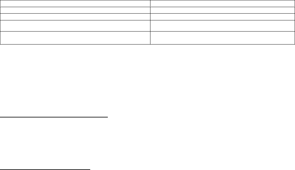
Connect unit to scalar network analyzer or spectrum analyzer with tracking generator. Set input level to –50
dBm. Sweep center frequency +/- 100 MHz. Set AGC off, coarse gain off fine gain to maximum. Verify
midband gain is 54 dB +/- 2 dB. See Fig. 1 for sample plot. Note: Plot shows booster at full gain. Shape
should be the same at lower gains.
• Passband
Verify gain within operating passband does not vary from reading in 6.8.2 by more than +/- 1 dB.
Verify rejection at offsets of +/- 100 MHz is at least 35 dB.
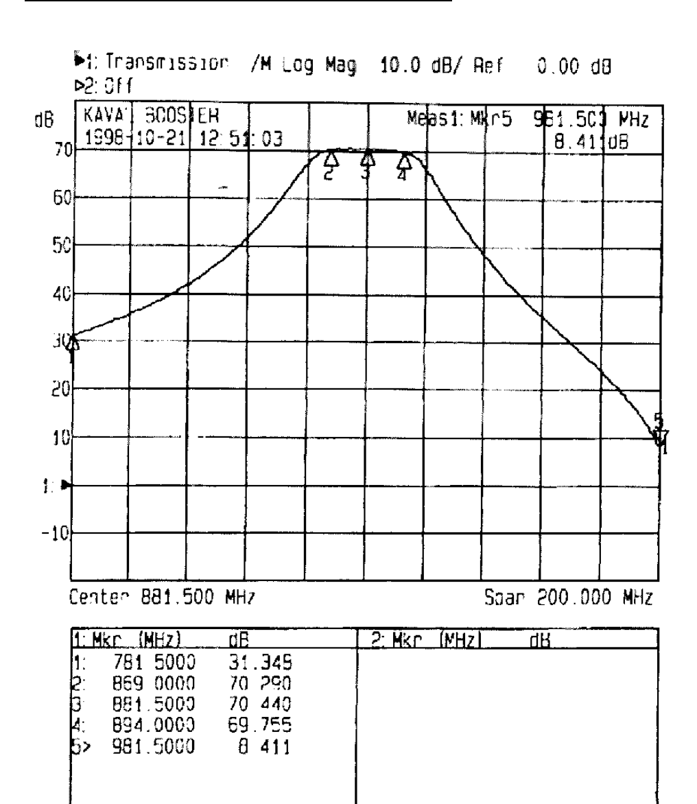
• Input Return Loss
Set coarse gain to on. Verify input return loss over operating passband is greater than 10 dB. See Fig. 2 for
sample plot.
• Single Tone Tests
• Saturated Power
Apply a single tone at input at a level of –30 dBm at the center of the application operating band. Verify
output power is at least +30 dBm.
• Coarse Gain Adjustment
Set coarse gain off. With input signal at a level of –50 dBm, measure output level. Set coarse gain on.
Adjust R21 to obtain an output level of 16 dB +/- 0.25 dB higher than reading obtained with coarse gain off.
• Maximum Gain
Calculate difference between output level and – 50 dBm. This is the maximum gain. Verify this to be +70
dB +/- 2 dB.
l Page 7Kaval Telecom Inc. - Company Secret DCD000000003
• AGC Alignment
With an input signal level of – 30 dBm, with coarse gain on, fine gain at max and AGC on, adjust R12 to obtain an output
level in accordance with the table below. Settings are derived using FCC recommended procedure for determining
channel loading of multichannel amplifiers.
APPLICATION AGC Single Carrier Target Level
Standalone Booster +20 dBm
Booster used with SMA 20W Amplifier +15 dBm
Booster used with TRL 35W Amp with +51dBm IP3 +10.5
Booster used with TRL 35W amp that conforms to +55.5
dBm IP3 +15 dBm
• Verification of Fine Gain Control
With a single carrier input level of –50 dBm, AGC off and all gains set to max, observe the output level while decreasing fine gain
step by step. Verify that steps are monotonic and that with fine gain set to minimum, overall gain is less than maximum gain by 16
dB +/- 0.7 dB. (Monotonic means that the steps are in the right order, that when you reduce gain by any 1 dB step, the gain
change is in the right direction. Some attenuator faults may result in steps getting out of order when you cross a high bit
boundary.)
• INSTALLATION OF BOTTOM COVER
Install labels (uplink/downlink) near 9 pin connectors. Ensure labels go with correct PCB boards.
Install bottom cover (to assembly using 16 #2-56 flat head screws.
• FINAL TEST AND INSPECTION
If required by customer contract, repeat swept measurement at full gain to produce a final plot for shipment to customer or
for file. This also verifies that cover installation did not disrupt the circuitry as gaskets were compressed.
Inspect housing for missing screws.
Affix nameplate with serial number.
Pack unit for shipment if applicable.
l Page 8Kaval Telecom Inc. - Company Secret DCD000000003
• FIGURE #1: TYPICAL BOOSTER RESPONSE WITH LID REMOVED
l Page 9Kaval Telecom Inc. - Company Secret DCD000000003
• FIGURE #2: TYPICAL BOOSTER INPUT RETURN LOSS
l Page 10 Kaval Telecom Inc. - Company Secret DCD000000003
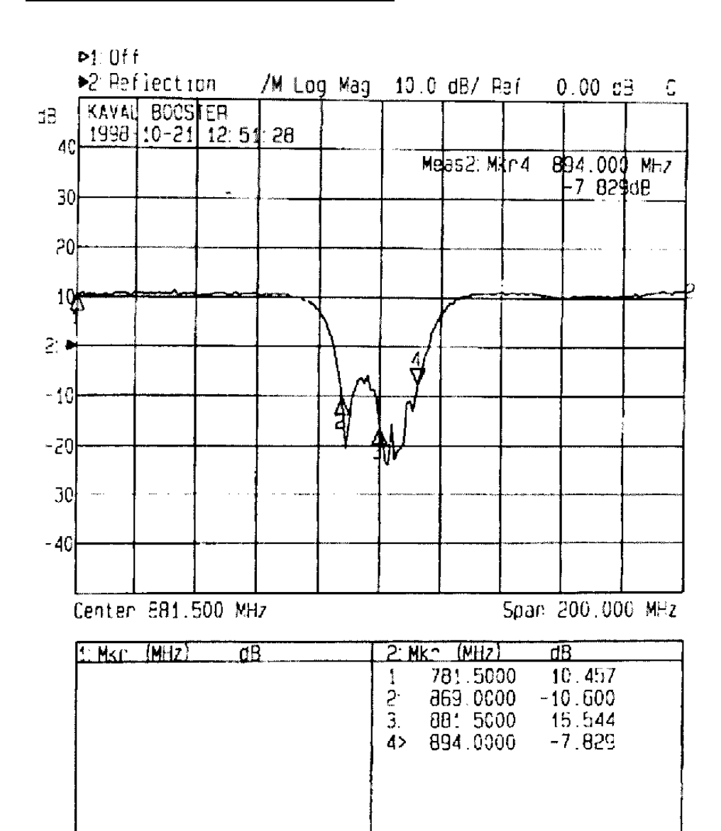
• FIGURE #3: ASSEMBLY DRAWING
3X 10-32 X .38 CAP SCREW
6X 10-32 X .88 CAP SCREW
72903-010
72900-002
72903-010
228271-01
228271-03
228271-07
228271-04
228271-05
050271-2E
3566-9128
228271-00
228271-02
010271-9F
22
010271-9ADWG NAME:
07-Aug-98
DATE:
CONYERS, GEORGIA 30012
1015 CONYERS EXECUTIVE PARK, SUITE 200
& ASSOCIATES, INC.
STEPHEN MAKK
OF
APPROVED
BY
DATE
REVISIONS
ECO
REV
DESCRIPTION
B
REV
FSCM NO.
DWG NO.
SHEET
SCALE
SIZE
l Page 11 Kaval Telecom Inc. - Company Secret DCD000000003
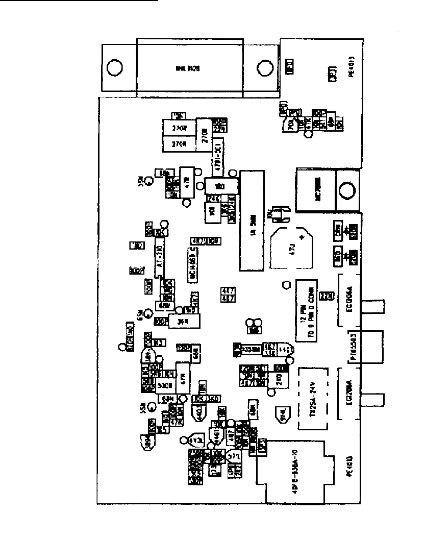
• FIGURE #4: BOARD OUTLINE #1
l Page 12 Kaval Telecom Inc. - Company Secret DCD000000003
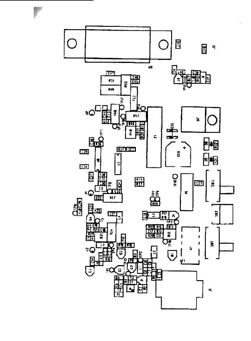
• FIGURE #5: BOARD OUTLINE #2
l Page 13 Kaval Telecom Inc. - Company Secret DCD000000003
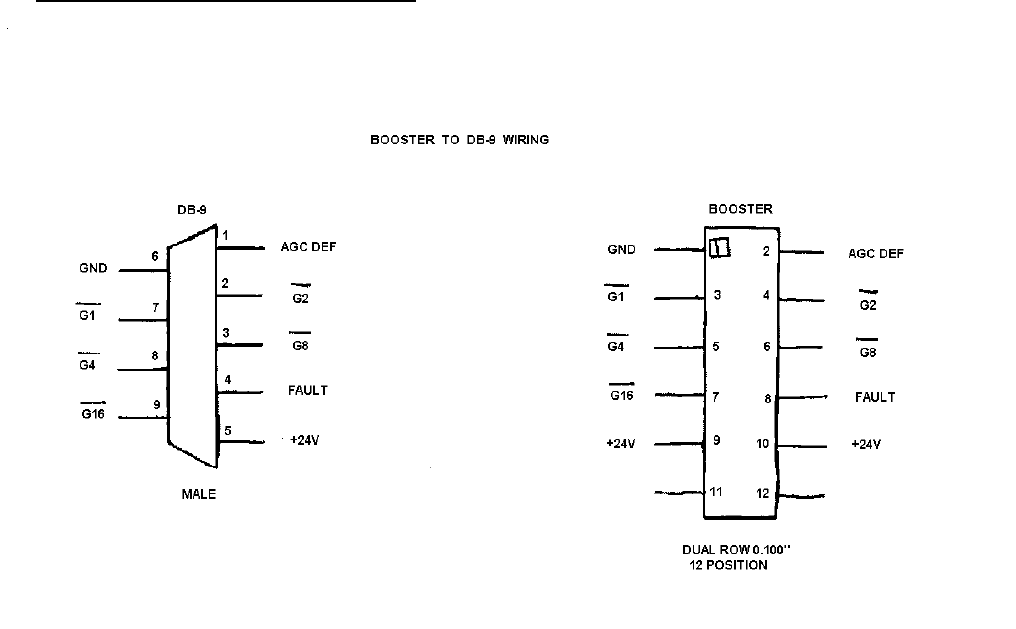
• FIGURE #6: BOOSTER TO DB-9 WIRING