User Manual

Datasheet
Version 1.0

02Version 1.0
1.0 Overview 03
2.0 Features 03
3.0 Specications 04
3.1 CPU 04
3.2 Memory 04
3.3 WiFi 04
3.4 Bluetooth 04
3.5 LTECAT–M1 04
3.6 RTC 04
3.7 Security 04
3.8 Hash/encryption 04
4.0 BlockDiagram 04
5.0 Pinout 05
6.0 PinDetails 06
6.1 RemappingPins 08
7.0 ESP32Peripherals 09
7.1 RTC 09
8.0 Programmingthedevice 10
8.1 UART 10
8.2 Wi–Fi 10
8.2.1 Telnet 10
8.2.2 FTP 10
9.0 Bootmodes 10
9.1 Bootloadermode 10
9.2 Safeboot 10
10.0 Power 11
10.1 Currentconsumptionbypower
modes/featuresrunningat3.7V 11
11.0 MemoryMap 12
11.1 Flash 12
11.2 RAM 12
11.3 ROMandeFuses 12
12.0 WiFi 13
12.1 Supportedfeatures 13
12.2 Specications 13
13.0 Bluetooth 14
13.1 Supportedfeatures 14
13.2 Specication 14
13.2.1 Receiver–BasicDataRate 14
13.2.2 Receiver–EnhancedDataRate 15
13.2.3 Receiver–BluetoothLE 16
13.2.4 Transmitter–BasicDataRate 17
13.2.5 Transmitter–EnhancedDataRate 18
13.2.6 Transmitter–BluetoothLE 19
14.0 LTECAT–M1 20
14.1 Supportedfeatures 20
14.2 Specications 20
14.2.1 SupportedLTEbands 20
14.3 SIMCardrequirements 20
14.4 Certiedcarriers 20
15.0 ElectricalCharacteristics 21
15.1 Absolutemaximumratings 21
15.2 Input/Outputcharacteristics 21
16.0 MinimumRecommendedCircuit 22
17.0 MechanicalSpecications 23
18.0 RecommendedLandPatterns 23
19.0 DesignConsiderations 24
19.1 AntennaImpedance 24
19.2 Deepsleeppower 24
19.3 Referencelayout 25
20.0 SolderingProle 26
21.0 OrderingInformation 27
22.0 Packaging 27
22.1 Reel 27
22.2 Tape 27
22.3 Box 27
23.0 Certication 28
today – the perfect enterprise grade platform for your
With WiFi, BLE and cellular LTE–CAT M1, the
03Version 1.0
1.0 Overview
G01 OEM Module is the latest Pycom triple–bearer
MicroPython enabled micro controller on the market
connected things. Create and connect your
things everywhere, fast.
2.0 Features
– Powerful CPU, BLE and state of the art WiFi radio. 1KM
Wi Range
– MicroPython enabled
– Can be directly surface mount inside your product like
a regular component
– Ultra–low power usage: a fraction compared to other
connected micro controllers
Supports narrowband LTE UE categories M1
One single chip for CAT M1
04Version 1.0
3.0 Specications
3.1 C PU
– Xtensa® dual–core 32–bit LX6 microprocessor(s), up
to 600 DMIPS
– Hardware oating point acceleration
– Python multi–threading
– An extra ULP–coprocessor that can monitor GPIOs,
the ADC channels and control most of the internal
peripherals during deep–sleep mode while only
consuming 25uA.
3.2 Memory
– RAM: 520KB + 4MB
– External ash: 8MB
3.3 WiFi
– 802.11b/g/n 16mbps
3.4 Bluetooth
– Low energy and classic
3.5 LTECAT–M1
–
– 3GPP release 13 LTE Advanced Pro
–
– Integrated baseband, RF, RAM memory and power
management
– Reduced TX power class option
– Peak power estimations:
TX current = 420mA peak @1.5Watt
RX current = 330mA peak @1.2Watt
– Extended DRX (eDRX) and PSM features for long
sleep duration use cases
3.6 RTC
– Running at 150kHz
3.7 Security
– SSL/TLS support
– WPA Enterprise security
3.8 Hash/encryption
– SHA
– MD5
– DES
– AES
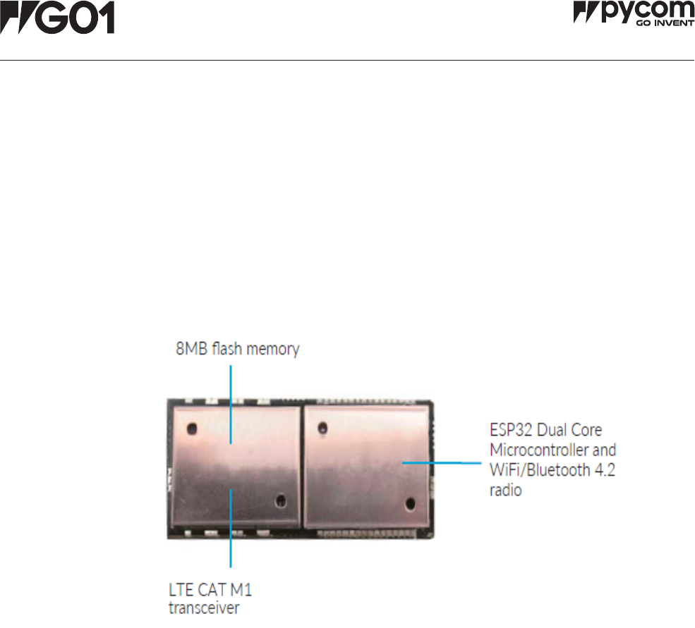
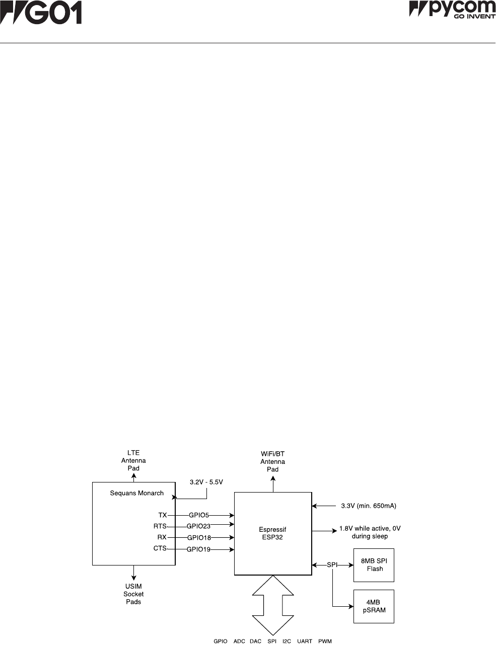
4.0 BlockDiagram
Figure 1 – System block diagram
05Version 1.0
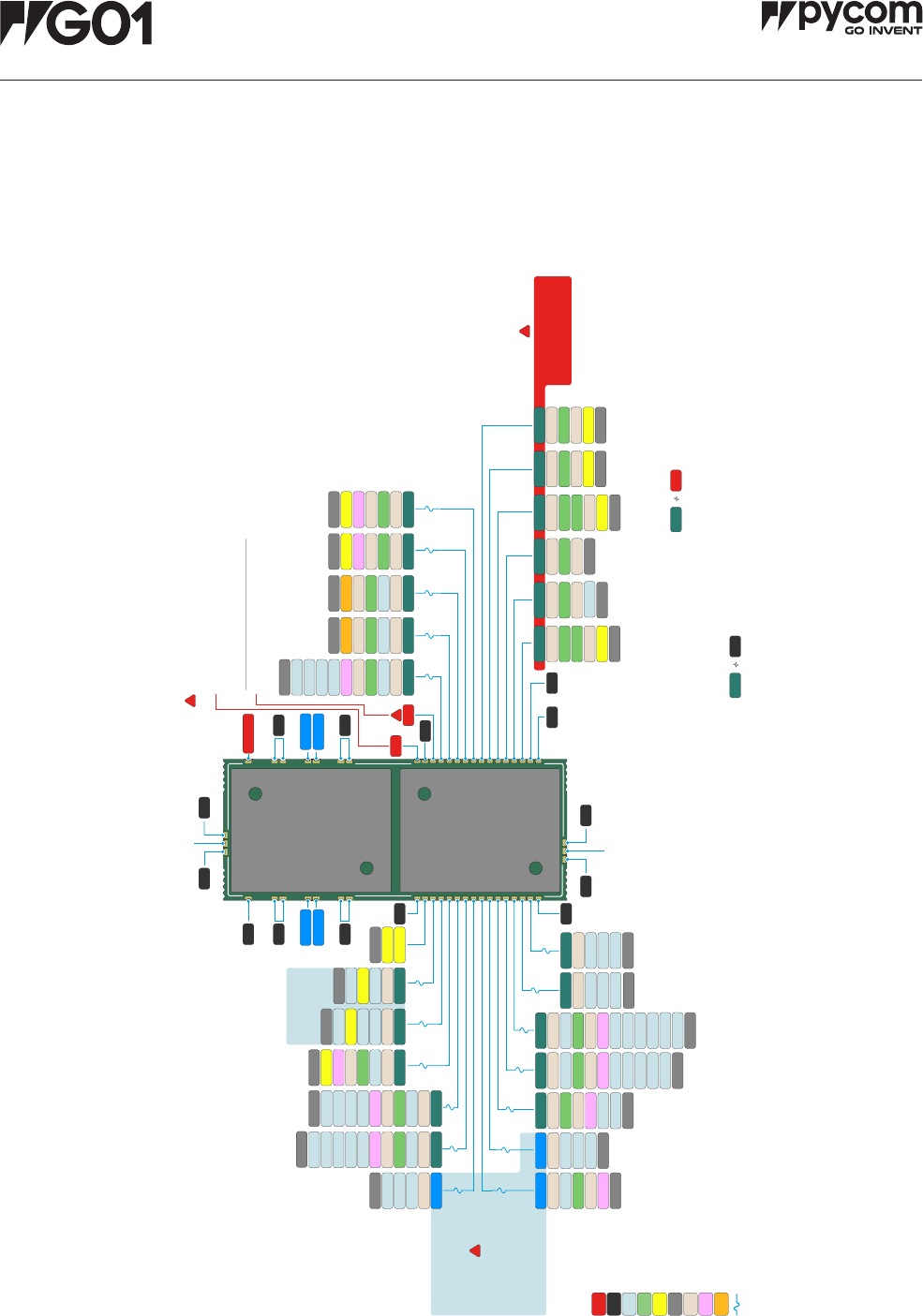
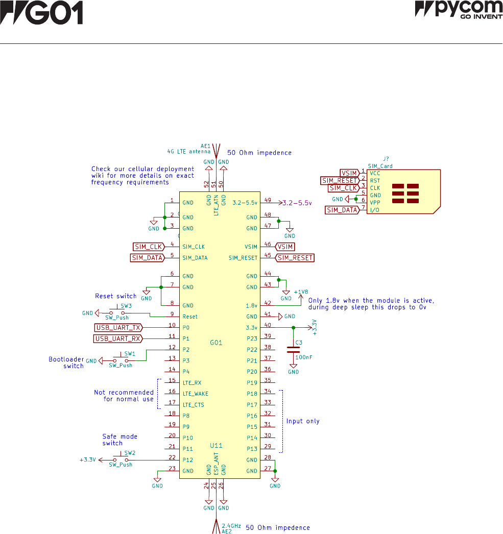
5.0 Pinout
Figure 2 – Module pinout diagram
Note: The ESP32 supports remapping its peripherals to alternative pins. See below for a detailed list.
Pinout diagram
Distributed and manufactured by Pycom Ltd.
Registered office:
High Point, 9 Sydenham Road, Guildford, Surrey GU1 3RX, UK
Copyright © 2017 by Pycom Ltd. All rights reserved. No part of this
document may be reproduced, distributed, or transmied in any form
or by any means, including photocopying, recording, or other
electronic or mechanical methods, without the prior wrien
permission of Pycom Ltd, except in the case of brief quotaons
embodied in crical reviews and certain other noncommercial
uses permied by copyright law.
To order contact sales@pycom.io
Power
GND
Serial Pin
Analog Pin
Control
Physical Pin
Port Pin
Touch Pin
DAC Pin
PMW Pin
Low Level Bootloader
P2 +GND
Boot modes and safe boot
P12 +3V3
1-3 sec Safe boot, latest firmware is selected
4-6 sec Safe boot, previous user update selected
7-9 sec Safe boot, the factory firmware is selected
GND
GND
GNDGND
GNDGND
GND
GND
GND
GND
GND
LTE CAT M1 Antenna
WiFi / Bluetooth
Antenna
P11
GPIO
22
MISO
U0
RTS
VSPI
WP
EMAC
TXD1
39
P10
GPIO
13
SCL
CLK
MT
CK
HSPI
ID
SD
DATA3
HS2
DATA3
EMAC
RXER
ADC2_4
RTCIO
14
Touch
4
20
P9
GPIO
12
SDA
MT
DI
HSPI
Q
SD
DATA2
HS2
DATA2
EMAC
TXD3
ADC2_5
RTCIO
15
Touch
5
18
P8
GPIO
2
HSPI
WP
ADC2_2
RTCIO
12
Touch
2
22
GPIO
19
U0
CTS
VSPI
Q
EMAC
TXD0
38
GPIO
27
EMAC
RXDV
ADC2_7
RTCIO
17
Touch
7
16
GPIO
5
VSPI
CS0
HS1
DATA6
EMAC
RXCLK
34
P4
GPIO
15
RX1
MT
D0
HSPI
CS0
SD
CMD
HS2
CMD
EMAC
RXD3
ADC2_3
RTCIO
13
Touch
3
21
P3
GPIO
4
HSPI
HD
SD
DATA1
HS2
DATA1
EMAC
TXER
ADC2_0
RTCIO
10
Touch
0
TX1
24
P12
GPIO
21
MOSI
42
VSPI
HD
EMAC
TXEN
P2
GPIO
0
CLK
OUT1
EMAC
TXCLK
ADC2_1
RTCIO
11
Touch
1
23
P1
GPIO
1
U0
TXD
CLK
OUT3
EMAC
RXD2
TX0
41
P0
GPIO
3
CLK
OUT2
U0
RXD
RX0
40
RST
9
ChipPU
PROGRAM
Port
GND
3V3
!
Only Input pins!
No pullup/pulldown
internal resistance
!
Absolute MAX per pin 12mA
recommended 6mA
!
ADC2_6
P23
GPIO
14
EMAC
TXD2
RTCIO
16
Touch
6
MT
MS
HSPI
CLK
SD
CLK
HS2
CLK
17
P22
GPIO
25
ADC2_8
EMAC
RXD0
RTCIO
6
DAC_1
14
P21
GPIO
26
ADC2_9
EMAC
RXD1
RTCIO
7
DAC_2
15
P20
GPIO
33
ADC1_5
RTCIO
8
Touch
8
XTAL
32
13
P19
GPIO
32
ADC1_4
RTCIO
9
Touch
9
XTAL
32
12
P18
GPIO
34
ADC1_6
RTCIO
4
VDET
1
10
P17
GPIO
35
ADC1_7
RTCIO
5
VDET
2
11
P16
GPIO
39
ADC1_3
ADC
PA
RTCIO
3
Sens
VN
8
P15
GPIO
38
ADC1_2
RTCIO
2
7
P14
GPIO
37
ADC1_1
RTCIO
1
6
P13
GPIO
36
ADC
PA
ADC1_0
RTCIO
0
Sens
VP
5
GND
1V8
Outputs 1V8 while the module
is in active mode, and drops
to 0V during deep sleep
GND
Supply with a stable 3V3 power source
capable of delivering at least 950mA
Connected to
the LTE radio
!
LTE_CTS
LTE_WAKE
LTE_RX
VSIM
SIM_RESET
SIM_CLK
SIM_DATA
3.2-5.5V
SD
DATA0
23/01/18

06Version 1.0
6.0 PinDetails
Table 1 – Module pinout
Module
Pin
ESP32
GPIO
Pin
Name DefaultFunction ADC PWM RTC† Notes
1 – – Ground
2 – – Ground
3 – – Ground
4 – – USIM Clock
5 – – USIM I/O
6 – – Ground
7 – – Ground
8 – – Ground
9 – – Reset Active Low
10 3P0 RX0
(Programming)
Used by the bootloader and to program
the module
11 1P1 TX0
(Programming)
Used by the bootloader and to program
the module
12 0P2 2* If tied to GND during boot the device will
enter bootloader mode
13 4P3 TX1 2*
14 15 P4 RX1 2* JTAG TDO, SD card CMD
15 5 – Sequans modem
RX Not recommended for external use
16 27 –Sequans modem
Interrupt 2* Not recommended for external use
17 19 –Sequans modem
CTS Not recommended for external use
18 2P8 2* SD card DAT0
19 12 P9 SDA 2* JTAG TDI

07Version 1.0
6.0 PinDetails
Table 1 – Module pinout
Module
Pin
ESP32
GPIO
Pin
Name DefaultFunction ADC PWM RTC† Notes
20 13 P10 SCL (I2C) / CLK
(SPI) 2* JTAG TCK
21 22 P11 MOSI
22 21 P12 If tied to 3.3V during boot the device
enters safe boot mode, JTAG MISO
23 – – Ground
24 – – Ground
25 – – WiFi/BT antenna 50 Ohm impedance required
26 – – Ground
27 – – Ground
28 – – Ground
29 36 P13 1Input only
30 37 P14 1Input only
31 38 P15 1Input only
32 39 P16 1Input only
33 35 P17 1Input only
34 34 P18 1Input only
35 32 P19 1
36 33 P20 1Connected to the on–board RGB LED
37 26 P21 2* DAC
38 25 P22 2* DAC
39 14 P23 2* JTAG TMS, SD card SCLK

08Version 1.0
6.0 PinDetails
Table 1 – Module pinout
† The pins on the RTC power domain can be used during deep sleep, specically GPIO pins will maintain their state while in deep sleep.
* ADC2 is currently not supported in the micropython rmware
Module
Pin
ESP32
GPIO
Pin
Name DefaultFunction ADC PWM RTC† Notes
40 – – 3.3V input This supply should be able to source
650mA
41 – – Ground
42 – – 1.8V Output Only when the device is active, during
deep sleep this drops to 0V
43 – – Ground
44 – – Ground
49 – – 3.2–5.5V input Powers the Sequans cellular modem
50 – – Ground
51 – – LTE CAT–M1
antenna 50 Ohm
impedance required
52 – – Ground
–23 –Sequans modem
TX
–18 –Sequans modem
RTS
6.1 RemappingPins
The ESP32 features comprehensive pin remapping
functionality. This allows peripherals to be mapped onto
almost any available GPIO pins. The above table merely
shows the default assignments. For example, the
default mapping has the SPI and I2C clocks overlapping,
meaning both cannot be used simultaneously without
remapping one to a different pin. For a detailed guide
of what peripheral can be assigned to what pins please
read “Appendix A – ESP32 Pin Lists” of the ESP32
datasheet.
09Version 1.0
7.0 ESP32Peripherals
Table 2 – Peripherals
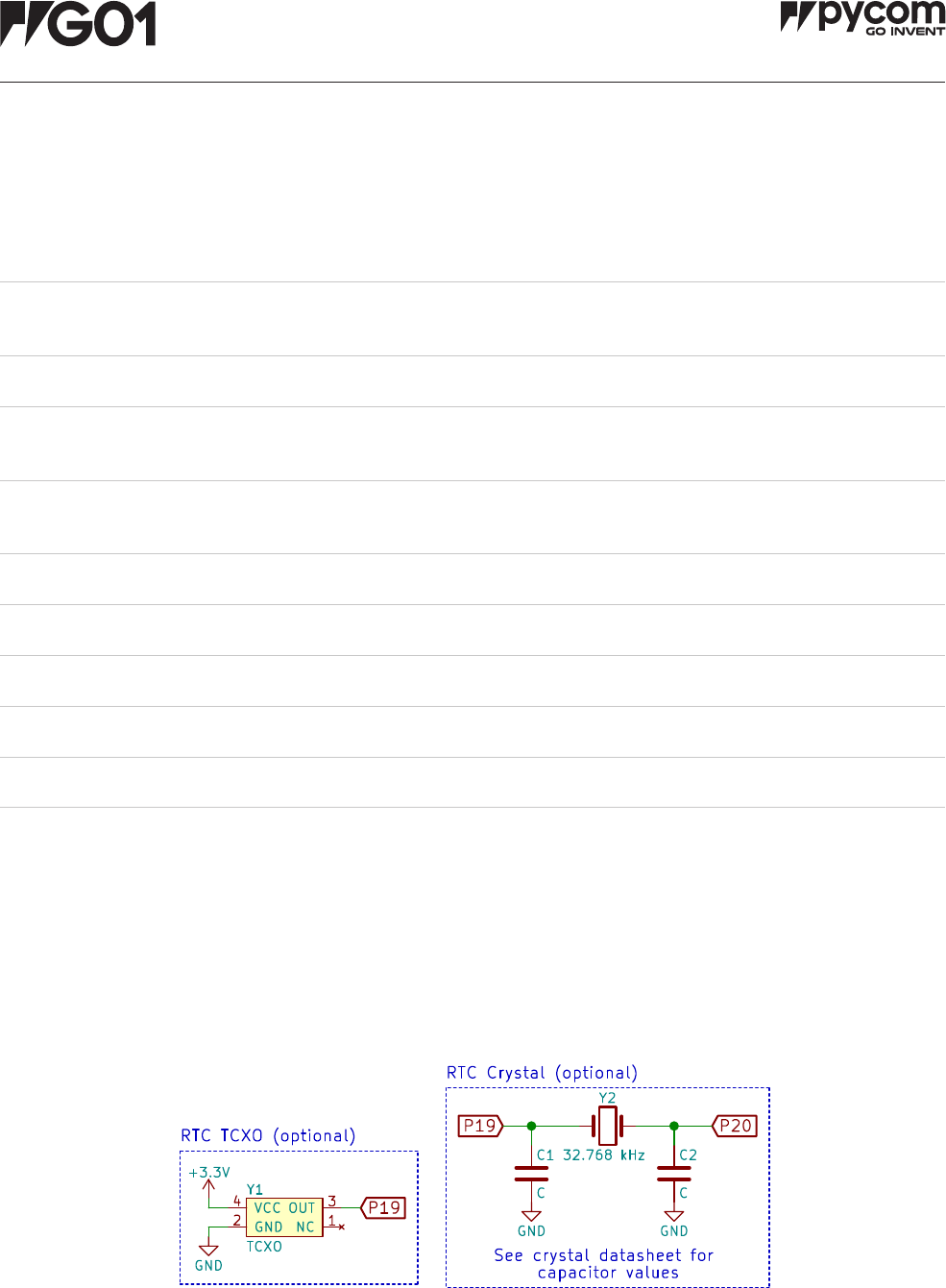
Figure 3 – External RTC crystal circuits
* Requires an external CAN bus transceiver, we recommend the SN65HVD230 from Texas Instruments.
For a more detailed description of the ESP32 peripherals
along with peripherals not currently supported by our
rmware, please check the ESP32 datasheet.
7.1 R TC
Our modules by default all use the internal RC oscillator
at 150kHz for the RTC. If you require better accuracy/
stability you can connect a 32.768 kHz crystal (or TCXO)
externally on pins P19 and P20 (or P19 for a TXCO)
Peripheral Count Pins
UART 3Remappable to any GPIO.
Note: P13–18 can only be mapped to RX or CTS since they are input only.
I2C 2Remappable to any GPIO except P13–18 since they are input only and I2C is bi–directional.
SPI 3Remappable to any GPIO.
Note: P13–18 can only be mapped to MISO since they are input only.
CAN* 1Remappable to any GPIO.
Note: P13–18 can only be mapped to RX since they are input only.
JTAG 1 TDO = P4, TDI = P9, TCK = P10, TMS = P24
PWM 1 All GPIO except P13–18 which are input only
ADC 18 Fixed mapping, see Table 1, Only ADC 1 is supported in our micropython rmware.
DAC 2 Only available on P21 and P22
SD 1 DAT0 = P8, SCLK = P23, CMD = P4

10Version 1.0
8.0 Programmingthedevice
8.1 UA RT
By default, the modules run an interactive python
REPL on UART0 which is connected to P0 (RX) and P1
(TX) running at 115200 baud. Code can be run via this
interactive REPL or you can use our PyMakr plugin for
Atom or Visual Studio Code to upload code to the board.
8.2 Wi–Fi
By default, the G01 also acts as a Wi–Fi access point
SSID: gpy–wlan–XXXX
Password: www.pycom.io
Once connected to the G01’s Wi–Fi network you can
access it in two ways.
8.2.1 Telnet
Running on port 23 is a telnet server. This acts in a
very similar way to the UART. It presents you with an
interactive REPL and can also be used to upload code
via PyMakr.
8.2.2 FTP
The G01 also runs a FTP server that allows you to copy
les to and from the device, include an SD card if one is
connected. To connect to this FTP server, you need to use
plain FTP (un–encrypted) with the following credentials:
User: micro
Password: python
9.0 Bootmodes
9.1 Bootloadermode
In order to update the rmware of the G01 device, it
needs to be placed into bootloader mode. In order to
do this, P2 needs to be connected to ground when the
device reboots. Once in bootloader mode you can use
the Pycom rmware update tool to update to the latest
ofcial rmware. If you are developing your own rmware
based on our open–source rmware, a ashing script is
provided with the source code.
9.2 Safeboot
The micropython rmware features a safe boot feature
that skips the boot.py and main.py scripts and goes
straight to the REPL. This is useful if the device is
programmed with code that causes the device to crash or
become inaccessible. To access this mode, you need to
connect P12 to 3.3V and reset the device. Upon entering
safe boot mode, the on–board LED will begin to blink
orange. Depending on the duration the pin is held at 3.3V,
a different rmware will be run.
Table 3 – Boot modes
0–3Seconds 3–6Seconds
Current rmware without running
boot.py or main.py
Previous rmware if the rmware was uploaded via OTA
(without running boot.py and main.py)

11Version 1.0
10.1 Currentconsumptionbypowermodes/featuresrunningat3.3V
Table 4 – Power consumption by feature
10.0 Power
The G01 features an on–board voltage regulator that
takes 3.5V – 5.5V from the VIN pin and regulates it to
3.3V. It is important to only use the 3.3V as an output
and not try to feed 3.3V into this pin as this could
damage the regulator.
Mode Min Avg. Max Units
Idle (no radios) –37 –mA
LTE Transmit –173 285 mA
LTE Attached –75 –mA
WiFi AP – 117 –mA
WiFi client –130 –mA
Bluetooth –113 –mA
Deep sleep –13.5 –mA

12Version 1.0
11.0 MemoryMap
11.1 Flash
11.2 R AM
11.3 ROMandeFuses
Table 5 – Flash memory map
Table 6 – RAM memory map
Table 7 – Miscellaneous memory
Name Description Startaddress Size
NVS Non–volatile RAM area. Used by the NVS API 0x9000 0x7000
Firmware Slot 0 First rmware slot. Factory rmware is ashed here 0x10000 0x180000
OTA info Information about the current active rmware 0x190000 0x1000
Firmware Slot 1 Second rmware slot 0x1A0000 0x180000
File system 504KB le system on devices with 4MB ash 0x380000 0x7F000
Cong Cong area for LoRa, Sigfox and LTE 0x3FF000 0x1000
File system (2) 4MB le system on devices with 8MB ash 0x400000 0x400000
Name Description Size
On–chip SRAM Internal RAM memory used by the 2 xtensa CPUs 520KB
Fast RTC RAM Fast RAM area accessible by the xtensa cores during
boot and sleep modes 8KB
Slow RTC RAM Slow RAM area accessible by the Ultra–Low Power
Coprocessor during deep sleep 8KB
External pSRAM External QSPI RAM memory clocked @ 40MHz 4MB
Name Description Size
On–chip ROM Contains core functions and boot code. 448KB
eFuse
256 bits are used for the system (MAC address and
chip conguration) and the remaining 768 bits are
reserved for customer applications, including Flash–
Encryption and Chip–ID
1kbit

13Version 1.0
12.0 WiFi
12.1 Supportedfeatures
– 802.11 b/g/n
– 802.11 n (2.4 GHz), up to 150 Mbps
– 802.11 e: QoS for wireless multimedia technology
– WMM–PS, UAPSD
– A–MPDU and A–MSDU aggregation
– Block ACK
– Fragmentation and defragmentation
– Automatic Beacon monitoring/scanning
– 802.11 i security features: pre–authentication and TSN
– Wi–Fi Protected Access (WPA/WPA2/WPA2–
Enterprise/Wi–Fi Protected Setup (WPS)
– Infrastructure BSS Station mode/SoftAP mode
– Wi–Fi Direct (P2P), P2P Discovery, P2P Group Owner
mode and P2P Power Management
12.2 Specications
Table 8 – WiFi specications
Description Min Typ. Max Unit
Input Frequency 2412 –2462 MHz
Output power of PA for 11b mode 20.48 21.31 22.13 dBm
Sensitivity
DSSS, 1Mbps – – 98 dBm
CCK, 11 Mbps – – 91 dBm
OFDM, 6 Mbps – – 93 dBm
OFDM, 54 Mbps – – 75 dBm
HT20, MCS0 – – 93 dBm
HT20, MCS7 – – 73 dBm
HT40, MCS0 – – 90 dBm
HT40, MCS7 – – 70 dBm
MCS32 – – 89 dBm
Adjacent channel rejection
OFDM, 6 Mbps – 37 –dB
OFDM, 54 Mbps – 21 –dB
HT20, MCS0 – 37 –dB
HT20, MCS7 – 20 –dB

14Version 1.0
13.0 Bluetooth
13.1 Supportedfeatures
– Compliant with Bluetooth v4.2 BR/EDR and BLE
specication
– class–2 transmitter without external power amplier
– Enhanced power control
– NZIF receiver with –97 dBm sensitivity
– Adaptive Frequency Hopping (AFH)
–Standard HCI based on SDIO/SPI/UART
–High–speed UART HCI, up to 4 Mbps
– BT 4.2 controller and host stack
– Service Discover Protocol (SDP)
– General Access Prole (GAP)
– Security Manage Protocol (SMP)
– ATT/GATT
– HID
– All GATT–based prole supported
– SPP–like GATT–based prole
– BLE Beacon
– A2DP/AVRCP/SPP, HSP/HFP, RFCOMM
– CVSD and SBC for audio codec
– Bluetooth Piconet and Scatternet
13.2 Specication
13.2.1 Receiver–BasicDataRate
Table 9 – Receiver (basic data rate) specications
Parameter Min Typ. Max Unit
Sensitivity @0.1% BER ––94 –dBm
Maximum received signal @0.1% BER 0 – – dBm
Co–channel C/I – +7 –dB
Adjacent channel selectivity C/I
F = F0 + 1 MHz – – –6 dB
F = F0 – 1 MHz – – –6 dB
F = F0 + 2 MHz – – –25 dB
F = F0 – 2 MHz – – –33 dB
F = F0 + 3 MHz – – –25 dB
F = F0 – 3 MHz – – –45 dB
Out–of–band blocking performance
30Mhz ~ 2000MHz –10 – – dBm
2000MHz ~
2400MHz –27 – – dBm
2500MHz ~
3000MHz –27 – – dBm
3000MHz ~
12.5GHz –10 – – dBm
Intermodulation –36 – – dBm

15Version 1.0
Table 10 – Receiver (basic data rate) specications
13.2.2 Receiver–EnhancedDataRate
Parameter Min Typ. Max Unit
π/4 DQPSK
Sensitivity @0.1% BER ––90 –dBm
Maximum received signal @0.1% BER – 0 – dBm
Co–channel C/I – 11 –dB
Adjacent channel selectivity C/I
F = F0 + 1 MHz ––7 –dB
F = F0 – 1 MHz – –7 –dB
F = F0 + 2 MHz ––25 –dB
F = F0 – 2 MHz – –35 –dB
F = F0 + 3 MHz ––25 –dB
F = F0 – 3 MHz – –45 –dB
8DPSK
Sensitivity @0.1% BER
––84 –dBm
Maximum received signal @0.1% BER ––5 –dBm
C/I c–channel –18 –dB
Adjacent channel selectivity C/I
F = F0 + 1 MHz – 2 – dB
F = F0 – 1 MHz – 2 – dB
F = F0 + 2 MHz ––25 –dB
F = F0 – 2 MHz – –25 –dB
F = F0 + 3 MHz ––25 –dB
F = F0 – 3 MHz – –38 –dB

16Version 1.0
Table 11 – Receiver (BLE) specications
13.2.3 Receiver–BluetoothLE
Parameter Min Typ. Max Unit
Sensitivity @30.8% PER ––97 –dBm
Maximum received signal @30.8% PER 0 – – dBm
Co–channel C/I –+10 –dB
Adjacent channel selectivity C/I
F = F0 + 1MHz ––5 –dB
F = F0 – 1MHz – –5 –dB
F = F0 + 2MHz ––25 –dB
F = F0 – 2MHz – –35 –dB
F = F0 + 3MHz ––35 –dB
F = F0 – 3MHz – –45 –dB
Out–of–band blocking performance
30MHz ~
2000MHz –10 – – dB
2000MHz ~
2400MHz –27 – – dBm
2500MHz ~
3000MHz –27 – – dBm
3000MHz ~
12.5GHZ –10 – – dBm
Intermodulation –36 – – dBm

4
17Version 1.0
Table 12 – Transmitter (basic data rate) specications
13.2.4 Transmitter–BasicDataRate
Parameter Min Typ. Max Unit
RF transmit power - - dBm
RF power control range 3–5dBm
+20 dB bandwidth –0.9 –MHz
Adjacent channel transmit power
F = F0 + 1 MHz ––24 –dBm
F = F0 – 1 MHz – –16.1 –dBm
F = F0 + 2 MHz ––40.8 –dBm
F = F0 – 2 MHz – –35.6 –dBm
F = F0 + 3 MHz ––45.7 –dBm
F = F0 – 3 MHz – –40.2 –dBm
F = F0 + >3 MHz –45.6 –dBm
F = F0 – >3 MHz –44.6 –dBm
Δf1avg – – 155 KHz
Δf2max 133.7 KHz
Δf2avg/Δf1avg –0.92 – –
ICFT ––7 –KHz
Drift rate – 0.7 –KHz/50μs
Drift (1 slot packet) – 6 – KHz
Drift (5 slot packet) – 6 – KHz
--

18Version 1.0
Table 13 – Transmitter (enhanced data rate) specications
13.2.5 Transmitter–EnhancedDataRate
Parameter Min Typ. Max Unit
RF transmit power – 6.5 – dBm
Gain control step – -–dBm
RF power control range 5–8dBm
π/4 DQPSK max w0 ––0.72 –KHz
π/4 DQPSK max wi ––6 –KHz
π/4 DQPSK max |wi + w0| ––7.42 –KHz
8DPSK max w0 – 0.7 –KHz
8DPSK max wi – –9.6 –KHz
8DPSK max |wi + w0| –10 KHz
π/4 DQPSK modulation accuracy
RMS DEVM –4.28 – %
99% DEVM – – 30 %
Peak DEVM – 13.3 – %
8 DPSK modulation accuracy
RMS DEVM –5.8 – %
99% DEVM – 20 %
Peak DEVM – 14 – %
In–band spurious emissions
F = F0 + 1MHz ––34 –dBm
F = F0 – 1MHz – –40.2 –dBm
F = F0 + 2MHz ––34 –dBm
F = F0 – 2MHz – –36 –dBm
F = F0 + 3MHz ––38 –dBm
F = F0 – 3MHz – –40.3 –dBm
F = F0 ± >3MHz – – –41.5 dBm
EDR differential phase coding –100 – %
-

19Version 1.0
Table 14 – Transmitter (BLE) specications
13.2.6 Transmitter–BluetoothLE
Parameter Min Typ. Max Unit
RF transmit power – 3.5 – dBm
Gain control step – -–dBm
RF power control range 2–5dBm
Adjacent channel transmit power
F = F0 + 1MHz ––14.6 –dBm
F = F0 – 1MHz – –12.7 –dBm
F = F0 + 2MHz ––44.3 –dBm
F = F0 – 2MHz – –38.7 –dBm
F = F0 + 3MHz ––49.2 –dBm
F = F0 – 3MHz – –44.7 –dBm
F = F0 + >3MHz ––50 –dBm
F = F0 – >3MHz ––50 –dBm
Δf1avg – – 265 KHz
Δf2max 247 – – KHz
Δf2avg/Δf1avg ––0.92 – –
ICFT ––10 –KHz
Drift rate – 0.7 –KHz/50μs
Drift – 2 – KHz
-

20Version 1.0
14.0 LTECAT–M1
14.1 Supportedfeatures
– 3GPP release 13 LTE Advanced Pro
– Supports narrowband LTE UE categories M1
– Integrated baseband, RF, RAM memory and power
management
– Reduced TX power class option
– Extended DRX (eDRX) and PSM features for long
sleep duration use cases
Table 15 – LTE modem performance
Parameter Min Typ. Max Unit
Data rate
LTE Cat M1 in 1.4 Mhz, HD–FDD – DL – 300 –kbps
LTE Cat M1 in 1.4 Mhz, HD–FDD – UP – 375 –kbps
Table 16 – Supported LTE bands
Table 17 – SIM card speciciations
Table 18 – Certied carriers
14.2.1 SupportedLTEbands
14.3 SIMCardrequirements
14.4 Certiedcarriers
Bands TX/RX Frequencies
Low Bands 4, 12, 13
Parameter Min Typ. Max Unit
Form factor –Nano–SIM – –
Variant –USIM – –
Supply Voltage –1.8 – v
Carrier Country Network
Verizon US United States LTE CAT–M1
LTE BAND 4:1710-1755MHz(TX);2110-2155(RX)
LTE BAND 12:699-716MHz(TX);729-746(RX)
LTE BAND 13:777-787MHz(TX);746-756(RX)

21Version 1.0
15.0 ElectricalCharacteristics
15.1 Absolutemaximumratings
Table 19 – Absolute maximum ratings
Parameter Symbol Min Typ. Max Unit
Supply Input Voltage VIN 3.5 –5.5 V
Supply Output Current IOUT – – 1.2 A
Supply Output Voltage V3V3 –3.3 – V
Storage Temperature TSTR –––°C
Operating Temperature TOPR –40 –85 °C
Moisture Sensitivity Level MSL – 1 – –
Table 20 – Input/Output characteristics
15.2 Input/Outputcharacteristics
Parameter Symbol Min Typ. Max Unit
Input low voltage VIL –0.3 –0.25×V3V3 V
Input high voltage VIH 0.75×V3V3 – V3V3+0.3 V
Max Input sink current ISINK – 6 12 mA
Input leakage current IIL – – 50 nA
Input pin capacitance Cpin – – 2 pF
Output low voltage VOL 0.1×V3V3 – – V
Output high voltage VOH 0.8×V3V3 – – V
Max Output source current ISOURCE – 6 12 mA
22Version 1.0
16.0 MinimumRecommendedCircuit
Figure 4 – Minimum required circuit
23Version 1.0
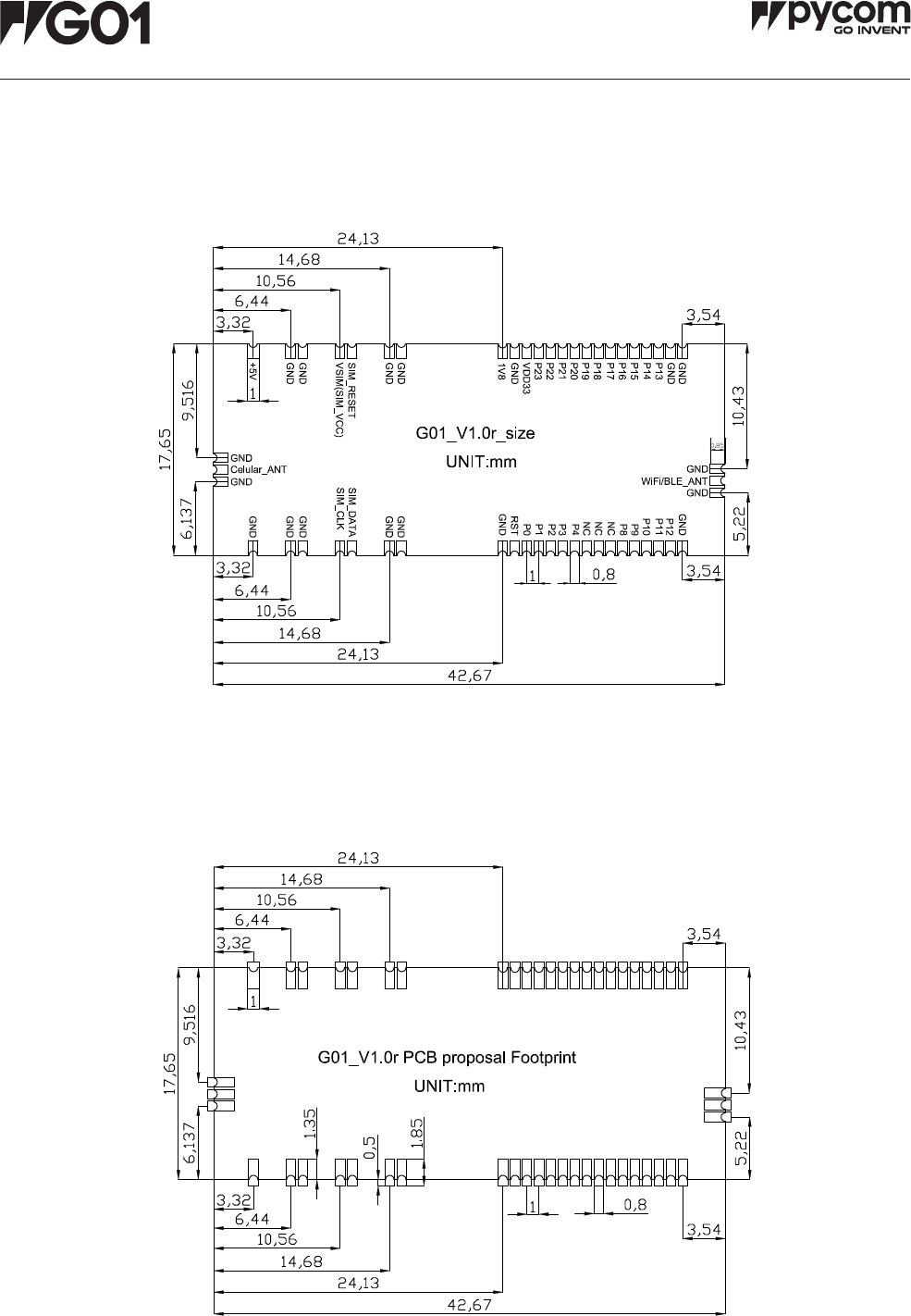
17.0 MechanicalSpecications
18.0 RecommendedLandPatterns
Figure 5 – Mechanical drawing (top down view)
Figure 6 – Recommended land pattern
24Version 1.0
19.0 DesignConsiderations
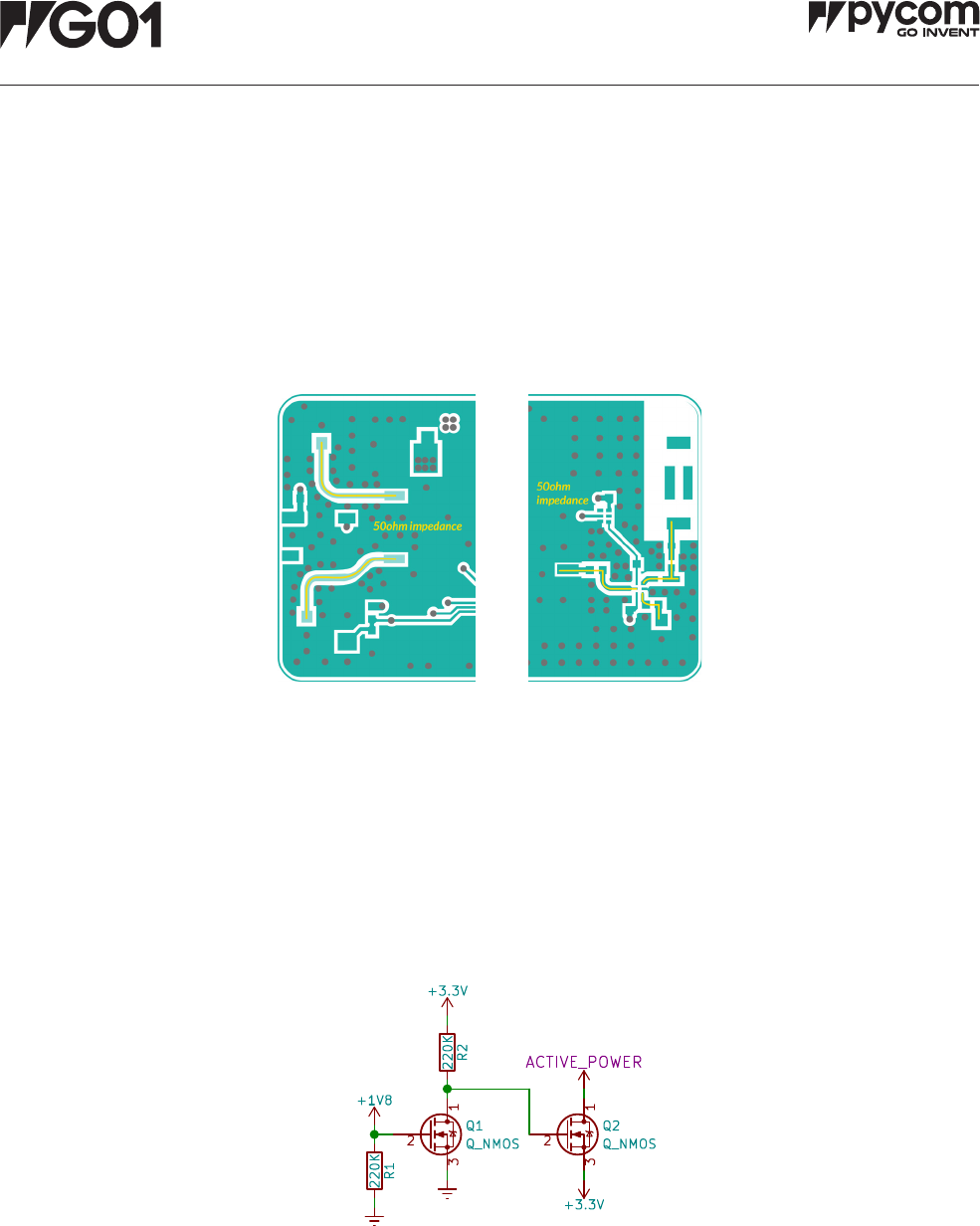
19.1 AntennaImpedance
Our OEM modules are intended to be used with a 50–ohm
antenna. They are also required to be connected to the
antenna by a 50–ohm grounded co–planar waveguide (as
shown in the reference design below with the yellow lines)
or a microstrip.
19.2 Deepsleeppower
When selecting a voltage regulator for your application
ensure that it has a low power mode, and that this is
enabled when the device enters deep sleep. We also
recommend cutting off power to all non–essential
components such as LEDs, logic gates, sensors etc.
when the device is in deep sleep. This can be done
using the circuit shown right:
This circuit uses the 1.8V output of the module to cut off
supply to non–essential circuitry. The 1.8V output is only
active when the module is running, when it goes to deep
sleep it drops to 0V. The non–essential circuitry is then
powered from the “ACTIVE_POWER” bus
Figure 7 – 50–ohm impedance antenna connections
Figure 8 – Power switch for deep sleep mode
25Version 1.0
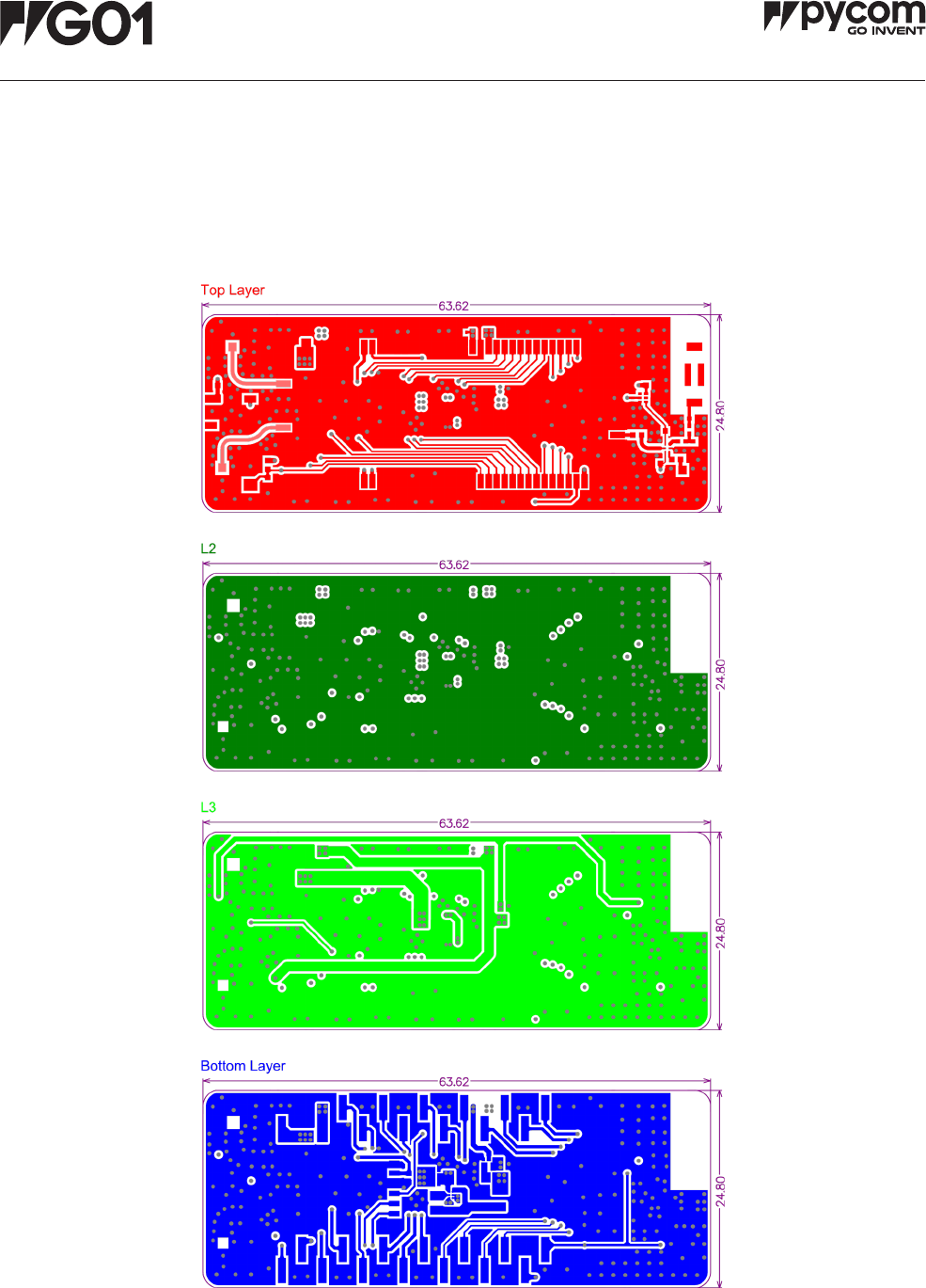
19.3 Referencelayout
Below you will nd the designs for our universal reference
board that ts all of our OEM modules. The design les can
be downloaded from our website.
Figure 9 – PCB layers for reference design – Units: mm
26Version 1.0
20.0 SolderingProle
Figure 10 – Reow soldering temperature prole
The above prole is based on Alpha CVP–390 solder paste, which has been successfully tested with our devices.
Table 21– Soldering prole temperatures
Stage Duration/Rate Temperature
Ramp to soak 2°C/s Ambient – 185°C
Soak 60s 185°C
Ramp to peak 1°C/s 240°C
Reow 45s >225°C
Cool down 2°C/s
27Version 1.0
21.0 OrderingInformation
Table 22 – Ordering information
Figure 11 – Mechanical drawing of reel – Units: mm
Figure 12 – Mechanical drawing of reel tape – Units: mm
Figure 13 – Mechanical drawing of reel box – Units: mm
ProductEAN Description
0700461341598 G01 – OEM version of GPy 1.0
0700461908845 Reel of 250 G01 OEM modules
0700461908968 Reel of 500 G01 OEM modules
22.0 Packaging
22.1 Reel
22.2 Tape
22.3 Box

28Version 1.0
23.0 Certication
FCC 2AJMTG01R
IC 22263–G01R
Copies of the certicates can be found on our website.
;7;u-Ѵollmb1-ঞomollbvvbomm|;u=;u;m1;
Statement
$_bv7;b1;1olrѴb;vb|_-u|ƐƔo=|_;!Ѵ;vĺr;u-ঞombv
v0f;1||o|_;=oѴѴobm]|o1om7bঞomvĹ
ŐƐő$_bv7;b1;l-mo|1-v;_-ul=Ѵbm|;u=;u;m1;ĺ
(2) This device must accept any interference received, including
bm|;u=;u;m1;|_-|l-1-v;m7;vbu;7or;u-ঞomĺ
&$Ĺ_-m];voulo7bC1-ঞomvmo|;ru;vvѴ-rruo;70|_;
party responsible for compliance could void the user's authority to
or;u-|;|_;;tbrl;m|ĺ
NOTE: This equipment has been tested and found to comply
with the limits for a Class B digital device, pursuant to Part 15 of
|_;!Ѵ;vĺ$_;v;Ѵblb|v-u;7;vb]m;7|oruob7;u;-vom-0Ѵ;
ruo|;1ঞom-]-bmv|_-ul=Ѵbm|;u=;u;1;bm-u;vb7;mঞ-Ѵbmv|-ѴѴ-ঞomĺ
This equipment generates uses and can radiate radio frequency
energy and, if not installed and used in accordance with
|_;bmv|u1ঞomvķl-1-v;_-ul=Ѵbm|;u=;u;m1;|ou-7bo
1ollmb1-ঞomvĺo;;uķ|_;u;bvmo]-u-m|;;|_-|bm|;u=;u;m1;
bѴѴmo|o11ubm-r-uঞ1Ѵ-ubmv|-ѴѴ-ঞomĺ=|_bv;tbrl;m|7o;v
1-v;_-ul=Ѵbm|;u=;u;m1;|ou-7boou|;Ѵ;bvbomu;1;rঞomķ_b1_
1-m0;7;|;ulbm;70|umbm]|_;;tbrl;m|o@-m7omķ|_;v;ubv
encouraged to try to correct the interference by one or more of the
following measur
es:
Ŋ!;oub;m|ouu;Ѵo1-|;|_;u
;1;bbm]-m|;mm-ĺ
Ŋm1u;-v;|_;v;r-u-ঞom0;|;;m|_;;tbrl;m|-m7u;1;b;uĺ
Ŋomm;1||_;;tbrl;m|bm|o-mo|Ѵ;|om-1bu1b|7b@;u;m|=uol
|_-||o_b1_|_;u;1;b
;ubv1omm;1|;7ĺ
ŊomvѴ||_;7;-Ѵ;uou-m;r;ub;m1;7u-7boņ$(|;1_mb1b-m=ou_;Ѵrĺ
RF Warning Statement
This device is intended only for OEM integrators
m7;u|_;=oѴѴobm]1om7bঞomvĹ
1) The antenna must be installed such that 20 cm is maintained
between the antenna and users, and
Ƒő $_;|u-mvlb;ulo7Ѵ;l-mo|0;1oŊѴo1-|;7b|_-mo|_;u
|u-mvlb;uou-m|;mm-ĺ
vѴom]-v|o1om7bঞomv-0o;-u;l;|ķ=u|_;u|u-mvlb;u
|;v|bѴѴmo|0;u;tbu;7ĺo;;uķ|_;bm|;]u-|oubvvঞѴѴ
u;vromvb0Ѵ;=ou|;vঞm]|_;bu;m7Ŋruo71|=ou-m-77bঞom-Ѵ
1olrѴb-m1;u;tbu;l;m|vu;tbu;7b|_|_bvlo7Ѵ;bmv|-ѴѴ;7ĺ$o
;mvu;1olrѴb-m1;b|_-ѴѴmomŊ|u-mvlb;u=m1ঞomv|_;_ov|
manufacturer is responsible for ensuring compliance with the
lo7Ѵ;Ővőbmv|-ѴѴ;7-m7=ѴѴor;u-ঞom-Ѵĺou;-lrѴ;ķb=-_ov|-v
ru;bovѴ-|_oub;7-v-mmbm|;mঞom-Ѵu-7b-|oum7;u|_;
;1Ѵ-u-ঞomo=om=oulb|ruo1;7u;b|_o|-|u-mvlb;u1;uঞC;7
module and a module is added, the host manufacturer is responsible
=ou;mvubm]|_-||_;-[;u|_;lo7Ѵ;bvbmv|-ѴѴ;7-m7or;u-ঞom-Ѵ
|_;_ov|1omঞm;v|o0;1olrѴb-m|b|_|_;-u|ƐƔmbm|;mঞom-Ѵ
u-7b-|ouu;tbu;l;m|vĺ
$_;lo7Ѵ;bvѴblb|;7|obmv|-ѴѴ-ঞom+ĺ
$_;lo7Ѵ;bvѴblb|;7|obmv|-ѴѴ-ঞombmlo0bѴ;ouC;7-rrѴb1-ঞomĺ
We hereby acknowledge our responsibility to provide guidance to
the host manufacturer in the event that they require assistance for
;mvubm]1olrѴb-m1;b|_|_;-u|ƐƔ"0r-u|u;tbu;l;m|vĺ
!$$$Ĺm|_;;;m||_-||_;v;1om7bঞomv1-mmo|
0;l;|Ő=ou;-lrѴ;1;u|-bmѴ-r|or1omC]u-ঞomvou1oŊѴo1-ঞom
b|_-mo|_;u|u-mvlb;uőķ|_;m|_;-|_oub-ঞombvmo
longer considered valid and the FCC ID cannot be used on the
Cm-Ѵruo71|ĺm|_;v;1bu1lv|-m1;vķ|_;bm|;]u-|oubѴѴ
0;u;vromvb0Ѵ;=ouu;;-Ѵ-ঞm]|_;;m7ruo71|Őbm1Ѵ7bm]|_;
|u-mvlb;uő-m7o0|-bmbm]-v;r-u-|;-|_oub-ঞomĺ
End Product Labeling
-m-Ѵm=oul-ঞom|o|_;m7&v;u
$_;bm|;]u-|ou_-v|o0;--u;mo||oruob7;bm=oul-ঞom|o
|_;;m7v;uu;]-u7bm]_o|obmv|-ѴѴouu;lo;|_bv!lo7Ѵ;bm
|_;v;uĽvl-m-Ѵo=|_;;m7ruo71|_b1_bm|;]u-|;v|_bvlo7Ѵ;ĺ
In the user manual of the end product, the end user has to be
informed that the equipment complies with FCC radio-frequency
;rovu;]b7;Ѵbm;vv;|=ou|_=ou-mm1om|uoѴѴ;7;mbuoml;m|ĺ
The end user has to also be informed that any changes or
lo7bC1-ঞomvmo|;ru;vvѴ-rruo;70|_;l-m=-1|u;u1oѴ7ob7
|_;v;uŝv-|_oub||oor;u-|;|_bv;tbrl;m|ĺ
The end user manual shall include all required regulatory
bm=oul-ঞomņ-umbm]-vv_obm|_bvl-m-Ѵĺ
This equipment complies with FCC radiation exposure
limits set forth for an uncontrolled environment .
This equipment should be installed and operated with
minimum distance 20cm between the radiator& your body.
The outside of final products that contains this
module device must display a label referring to theenclosed
module. This exterior label can use wording such as: "Contains
Transmitter Module FCC ID:2AJMTG01R,&*5 or
“Contains FCC ID:2AJMTG01R,&*5 , Any similar
wording that expresses the same meaning may be used.
6LQJOH0RGXODU$SSURYDO2XWSXWSRZHULVFRQGXFWHG7KLVGHYLFHLVWREHXVHGLQPRELOHRUIL[HG
DSSOLFDWLRQVRQO\$QWHQQDJDLQLQFOXGLQJFDEOHORVVPXVWQRWH[FHHG G%L
IRUWKHSXUSRVHRIVDWLVI\LQJWKHUHTXLUHPHQWVRI&)5
7KHDQWHQQDVXVHGIRUWKLVWUDQVPLWWHUPXVWEHLQVWDOOHGWRSURYLGHDVHSDUDWLRQ
GLVWDQFHRIDWOHDVWFPIURPDOOSHUVRQVDQGPXVWQRWEHFRORFDWHGRURSHUDWHGLQFRQMXQFWLRQZLWKDQ\
DQWHQQDRUWUDQVPLWWHUH[FHSWLQDFFRUGDQFHZLWK)&&PXOWLWUDQVPLWWHUHYDOXDWLRQSURFHGXUH&RPSOLDQFH
RIWKLVGHYLFHLQDOOILQDOSURGXFWFRQILJXUDWLRQVLVWKHUHVSRQVLELOLW\RIWKH*UDQWHH,QVWDOODWLRQRIWKLV
GHYLFHLQWRVSHFLILFILQDOSURGXFWVPD\UHTXLUHWKHVXEPLVVLRQRID&ODVV,,SHUPLVVLYHFKDQJHDSSOLFDWLRQ
FRQWDLQLQJGDWDSHUWLQHQWWR5)([SRVXUHVSXULRXVHPLVVLRQV(53(,53DQG
KRVWPRGXOHDXWKHQWLFDWLRQRUQHZDSSOLFDWLRQLIDSSURSULDWH
7 @ FDD (Band 4),
10.51 @ FDD (Band 12) and 10.94 @ FDD (Band 13)
ISED RSS Warning/ISED RF Exposure Statement
/HSUpVHQWDSSDUHLOHVWFRQIRUPHDX[&15G,6('DSSOLFDEOHVDX[DSSDUHLOV
UDGLRH[HPSWVGHOLFHQFH/H[SORLWDWLRQHVWDXWRULVpHDX[GHX[FRQGLWLRQV
VXLYDQWHV
ODSSDUHLOQHGRLWSDVSURGXLUHGHEURXLOODJHHW
OXWLOLVDWHXUGHODSSDUHLOGRLWDFFHSWHUWRXWEURXLOODJHUDGLRpOHFWULTXHVXEL
PrPHVLOHEURXLOODJHHVWVXVFHSWLEOHGHQFRPSURPHWWUHOHIRQFWLRQQHPHQW
,6('5)H[SRVXUHVWDWHPHQW
/HUD\RQQHPHQWGHODFODVVHEUHSHFWH,6('IL[DLHQWXQHQYLURQQHPHQWQRQ
FRQWU{OpV,QVWDOODWLRQHWPLVHHQ°XYUHGHFHPDWpULHOGHYUDLWDYHF
pFKDQJHXUGLVWDQFHPLQLPDOHHQWUHFPWRQFRUSV/DQFHXUVRXQHSHXYHQW
SDVFRH[LVWHUFHWWHDQWHQQHRXFDSWHXUVDYHFG¶DXWUHV
The product only use ceramic antenna for Bluetooth and wifi which the antenna gain is 1.3 dBi integration in a host
For IC , to meet RF exposure & ERP/ERIP, the maximum net gain of antennas allowed are 5.96 dBi @ FDD (Band 4),
7.14 @ FDD (Band 12) and 7.46 @ FDD (Band 13). The antenna(s) used for this transmitter must be installed to
provide a separation distance of at least 20 cm from all persons and must not be co-located or operating in
conjunction with any other antenna or transmitter.