Q MAC Electronics HF90 HF-90 User Manual Acrobat Distiller Job 5
Q-MAC Electronics Pty Ltd HF-90 Acrobat Distiller Job 5
UserManual.wiki
>
Q MAC Electronics
>
HF90 User Manual
>
Technical Manual
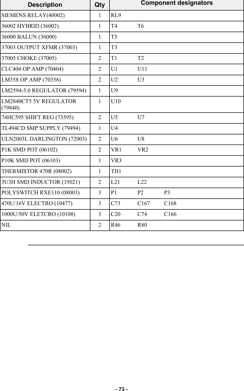
Contents
1.
User guide
2.
Technical manual
3.
Technical Manual
4.
User Guide
Technical Manual
Navigation menu
Upload a User Manual
Namespaces
Wiki Guide
HTML
PDF
Info
Views
User Manual
Discussion / Help
Navigation