User Manual

Copyright © 2011 Qisda Corporation. Confidential Property
M66 Design Guide
M66
GSM / GPRS Wireless Module
Design Guide
Rev. 0.0.1
2011/6/10
Copyright © 2008 Qisda Corporation. All rights reserved.
This document contains proprietary technical information which is the property of Qisda Corporation and is
issued in strict confidential and shall not be disclosed to others parties in whole or in parts without written
permission of Qisda Corporation.
The documents contain information on a product, which is under development and is issued for customer
evaluation purposes only.
Qisda may make changes to product specifications at any time, without notice.
Module Business Division
Mobile Communications BU
Qisda Corporation
18 Jihu Road, Nei-Hu, Taipei 114, Taiwan
Tel: +886-2-2799-8800
Fax: +886-2-2656-6398
http://Qisda.com

Version: 0.0.1 - 2 - 2011/6/10
M66 Design Guide
History
Version
Date
Notes
VER: 0.0.1
2011/6/10
First release

Version: 0.0.1 - 3 - 2011/6/10
M66 Design Guide
FCC Regulations:
This device complies with part 15 of the FCC Rules. Operation is subject to the following
two conditions: (1) This device may not cause harmful interference, and (2) this device must
accept any interference received, including interference that may cause undesired operation.
This device has been tested and found to comply with the limits for a Class B digital device,
pursuant to Part 15 of the FCC Rules. These limits are designed to provide reasonable
protection against harmful interference in a residential installation. This equipment generates,
uses and can radiated radio frequency energy and, if not installed and used in accordance with
the instructions, may cause harmful interference to radio communications. However, there is
no guarantee that interference will not occur in a particular installation If this equipment does
cause harmful interference to radio or television reception, which can be determined by
turning the equipment off and on, the user is encouraged to try to correct the interference by
one or more of the following measures:
-Reorient or relocate the receiving antenna.
-Increase the separation between the equipment and receiver.
-Connect the equipment into an outlet on a circuit different from that to which the receiver is
connected.
-Consult the dealer or an experienced radio/TV technician for help.
Changes or modifications not expressly approved by the party responsible for compliance
could void the user‘s authority to operate the equipment.
RF Exposure Information
This Modular Approval is limited to OEM installation for mobile and fixed applications
only. The antenna installation and operating configurations of this transmitter, including any
applicable source-based time-averaging duty factor, antenna gain and cable loss must satisfy
MPE categorical Exclusion Requirements of §2.1091.
The antenna(s) used for this transmitter must be installed to provide a separation distance of at
least 20 cm from all persons, must not be collocated or operating in conjunction with any
other antenna or transmitter, except in accordance with FCC multi-transmitter product
procedures.

Version: 0.0.1 - 4 - 2011/6/10
M66 Design Guide
The end user has no manual instructions to remove or install the device and a separate
approval is required for all other operating configurations, including portable configurations
with respect to 2.1093 and different antenna configurations.
Maximum antenna gain allowed for use with this device is 2 dBi.
When the module is installed in the host device, the FCC ID label must be visible through a
window on the final device or it must be visible when an access panel, door or cover is easily
re-moved. If not, a second label must be placed on the outside of the final device that contains
the following text: “Contains FCC ID: VRSGM6601”.

Version: 0.0.1 - 5 - 2011/6/10
M66 Design Guide
IC Regulations:
This device complies with Industry Canada licence-exempt RSS standard(s).
Operation is subject to the following two conditions:
(1) this device may not cause interference, and
(2) this device must accept any interference, including interference that may cause undesired
operation of the device.
Le présent appareil est conforme aux CNR d'Industrie Canada applicables aux appareils radio
exempts de licence.
L'exploitation est autorisée aux deux conditions suivantes: (1) l'appareil ne doit pas produire
de brouillage, et (2) l'utilisateur de l'appareil doit accepter tout brouillage radioélectrique subi,
même si le brouillage est susceptible d'en
This Class B digital apparatus complies with Canadian ICES-003.
Cet appareil numérique de la classe B est conforme à la norme NMB-003 du Canada.
This Category II radio communication device complies with Industry Canada Standard
RSS-310.
Ce dispositif de radiocommunication de catégorie II respecte la norme CNR-310 d’Industrie
Canada.
IMPORTANT NOTE:
IC Radiation Exposure Statement:
This equipment complies with IC RSS-102 radiation exposure limits set forth for an
uncontrolled environment. This equipment should be installed and operated with minimum
distance 20cm between the radiator & your body.

Version: 0.0.1 - 6 - 2011/6/10
M66 Design Guide
Under Industry Canada regulations, this radio transmitter may only operate using an antenna
of a type and maximum (or lesser) gain approved for the transmitter by Industry Canada. To
reduce potential radio interference to other users, the antenna type and its gain should be so
chosen that the equivalent isotropically radiated power (e.i.r.p.) is not more than that
necessary for successful communication.
Conformément à la réglementation d'Industrie Canada, le présent émetteur radio peut
fonctionner avec une antenne d'un type et d'un gain maximal (ou inférieur) approuvé pour
l'émetteur par Industrie Canada. Dans le but de réduire les risques de brouillage
radioélectrique à l'intention des autres utilisateurs, il faut choisir le type d'antenne et son gain
de sorte que la puissance isotrope rayonnée équivalente (p.i.r.e.) ne dépasse pas l'intensité
nécessaire à l'établissement d'une communication satisfaisante.
Labeling Requirements for the Host Device (from Section 3.2.1, RSS-Gen, Issue 3, December
2010): The host device shall be properly labeled to identify the module within the host device.
The Industry Canada certification label of a module shall be clearly visible at all times when
installed in the host device, otherwise the host device must be labeled to display the Industry
Canada certification number of the module, preceded by the words “Contains transmitter
module”, or the word “Contains”, or similar wording expressing the same meaning, as follows:
Contains transmitter module IC: 8729A-GM6601
This radio transmitter (identify the device by certification number, or model number if
Category II) has been approved by Industry Canada to operate with the antenna types listed
below with the maximum permissible gain and required antenna impedance for each antenna
type indicated. Antenna types not included in this list, having a gain greater than the
maximum gain indicated for that type, are strictly prohibited for use with this device.
Conformément à la réglementation d'Industrie Canada, le présent émetteur radio peut
fonctionner avec une antenne d'un type et d'un gain maximal (ou inférieur) approuvé pour
l'émetteur par Industrie Canada. Dans le but de réduire les risques de brouillage
radioélectrique à l'intention des autres utilisateurs, il faut choisir le type d'antenne et son gain
de sorte que la puissance isotrope rayonnée équivalente (p.i.r.e.) ne dépasse pas l'intensité
nécessaire à l'établissement d'une communication satisfaisante.

Version: 0.0.1 - 7 - 2011/6/10
M66 Design Guide
Index
1 POWER-ON / POWER-DOWN SEQUENCE .................................................................................... 9
1.1 POWER-ON SEQUENCE ........................................................................................................................... 9
1.2 SWITCHED ON ..................................................................................................................................... 10
1.3 M66 RESTARTS ...................................................................................................................................... 10
1.4 M66 SWITCH OFF .................................................................................................................................. 11
2 INITIALIZATION PROCEDURE ........................................................................................................ 12
3 SHORT MESSAGE .................................................................................................................................. 14
3.1 INITIALIZATION .................................................................................................................................... 14
3.2 SENDING A SMS ................................................................................................................................... 14
3.3 RECEIVING A SMS ................................................................................................................................. 15
4 VOICE CALL ............................................................................................................................................ 16
4.1 INITIALIZATION .................................................................................................................................... 16
4.2 MOBILE ORIGINATED CALL (MO) ......................................................................................................... 17
4.3 MOBILE TERMINATED CALL (MT) ........................................................................................................... 17
5 PPP DATA CALL ..................................................................................................................................... 18
5.1 GET READY FOR PPP DATA CALL............................................................................................................ 18
5.2 DIALING .............................................................................................................................................. 18
6 M2M ............................................................................................................................................................ 19
7 M66 INTERFACE .................................................................................................................................... 20
7.1 POWER ................................................................................................................................................ 21
7.2 UART.................................................................................................................................................. 23
7.3 AUDIO ................................................................................................................................................. 25
7.3.1 Microphone ..................................................................................................................................... 25
7.3.2 Receiver/Speaker ............................................................................................................................. 26
7.3.3 Grounding and Layout ...................................................................................................................... 27
7.4 SIM ..................................................................................................................................................... 28
7.4.1 ESD ................................................................................................................................................ 29
7.4.1.1 ESD protection diodes ................................................................................................................. 29
7.4.1.2 SIM holder ................................................................................................................................. 31
7.5 ANTENNA ............................................................................................................................................ 32
7.6 ANTENNA STATUS DETECTION APPLICATION .......................................................................................... 33

Version: 0.0.1 - 8 - 2011/6/10
M66 Design Guide
Version: 0.0.1 - 9 - 2011/6/10
M66 Design Guide
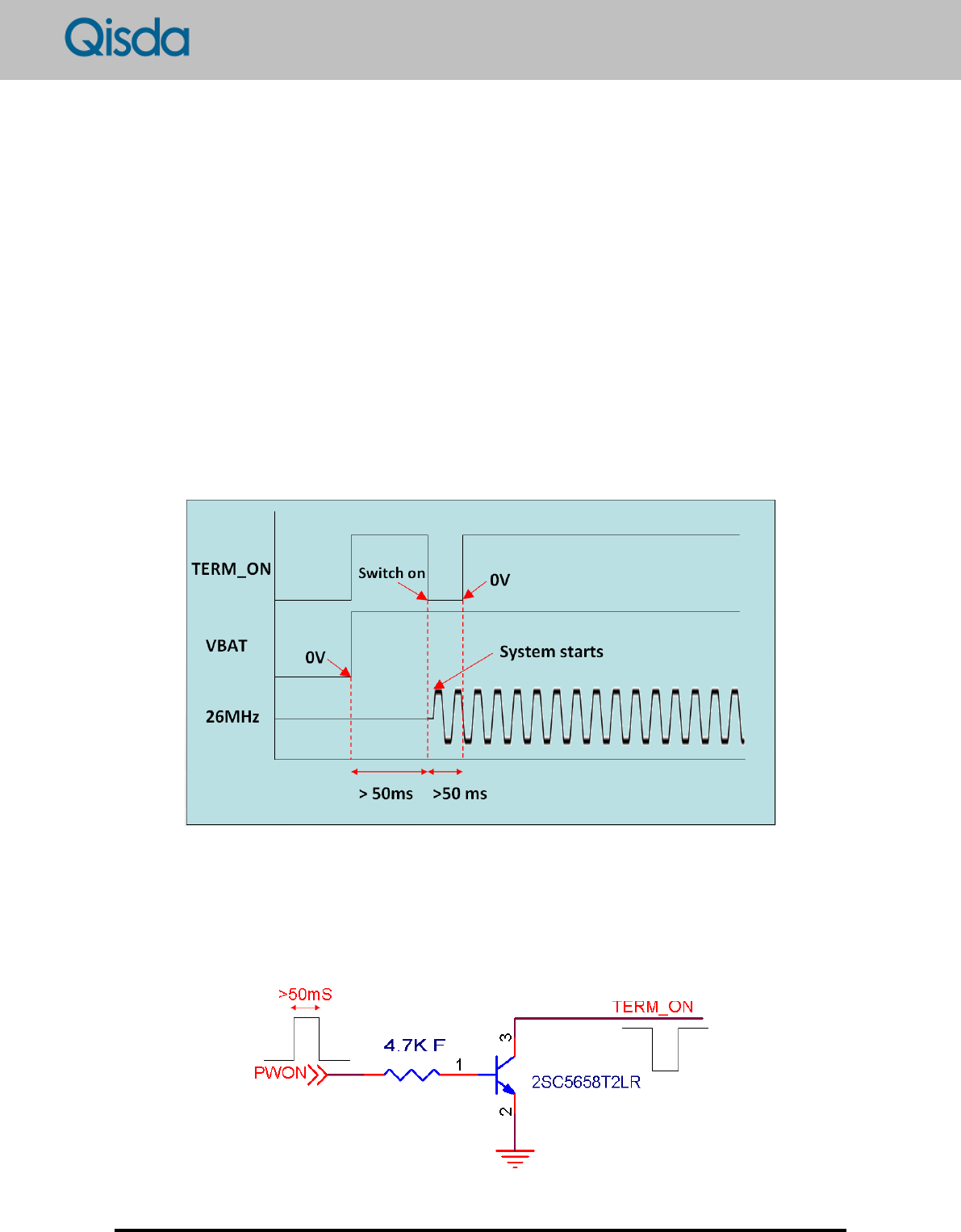
1 Power-on / Power-down Sequence
The operation voltage of M66 is between 3.3 and 4.2 V (A restricted operation range is
between 4.2 and 4.7 V). It is recommended to support a stable voltage in the proper range
which is between 3.8 and 4V.
1.1 Power-on sequence
1. The initial state:
VBAT: 0V
TERM_ON: LOW
2. Power on:
VBAT: HIGH (recommended: 3.8V-4V)
TERM_ON: HIGH
3. Switch on M66:
VBAT: Keep HIGH
TERM_ON: Keep LOW for 50ms then pull HIGH and remains.
Boot-up sequence
※ Please note that it is recommended to wait at least 50ms to pull LOW the TERM_ON pin
after power on (Put VBAT as HIGH). The system will not start if TERM_ON is LOW
before power on.
※ An open-collector circuit is needed when using MPU (client) to control the TERM_ON
pin.
Version: 0.0.1 - 10 - 2011/6/10
M66 Design Guide
1.2 Switched on
The factory default baud rate of M66 is 9600. The prompt”AT-Command Interpreter ready”
is output via UART1 after switched on.
LED status indication:The LPG pin (PIN 13) of M66 is used to indicate the M66/network
status. The LPG outputs different kind of pattern as follows:
M66/Network status
LPG pattern(unit:sec)
M66 startup
Always High
Power saving mode (Deep sleep mode)
Always Low
No network
(No SIM、PIN required、Not registered…)
High: 0.1,Low: 0.9
Registered and idle
High: 0.1,Low: 2.9
Connected(MO/MT Call)
Always High
GPRS transmitting/receiving data
Blinking(Note1)
Note 1:While in data mode, the LPG pattern is blinking if data is transmitting or receiving.
And the LPG keeps LOW if there is no data transmitting/receiving.
1.3 M66 restarts
1. General restart procedure:
a. AT+CFUN=0, stop all network-related action.
b. AT%RST to restart M66.
2. Emergency restart procedure:
a. In case there is no response of any AT commands.
b. Pull EMERG_OFF low for 50ms and then pull high.
c. Proceed the startup procedure(Please refer to 1.1)
Version: 0.0.1 - 11 - 2011/6/10
M66 Design Guide
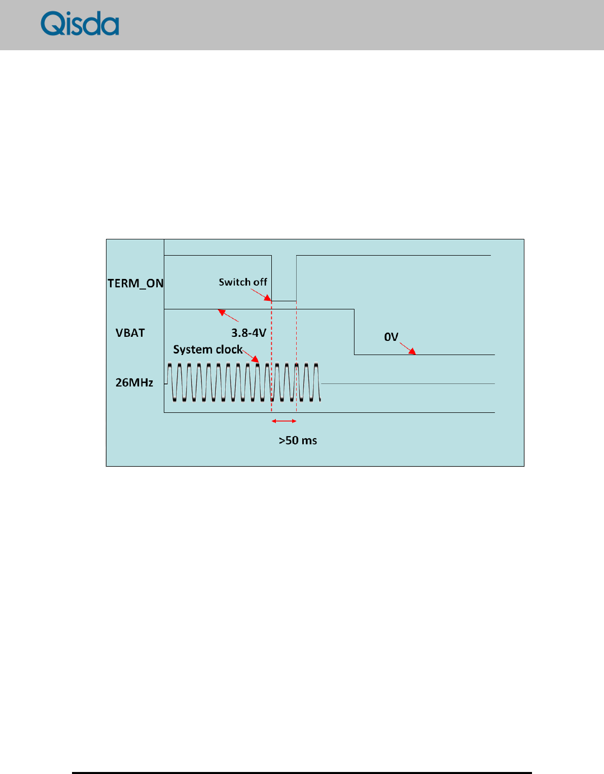
1.4 M66 switch off
1. SW switch off procedure:
a. AT+CFUN=0, stop all network-related action.
b. AT%MSO, switch off M66.
c. Remove VBAT.
2. HW switch off procedure:
a. AT+CFUN=0, stop all network-related action.
b. Pull TERM_ON low for 50ms and then pull high to shutdown M66.
c. Remove VBAT.

Version: 0.0.1 - 12 - 2011/6/10
M66 Design Guide
2 Initialization procedure
In this chapter, it describes the initialization procedure when using M66.
A suggested procedure and description of initialization.
AT
OK
ATE0
OK
AT%TSIM
%TSIM 1
OK
AT+CPIN?
+CPIN: READY
OK
AT+CSQ
+CSQ: 28,99
OK
AT+CREG=1
OK
AT+COPS?
+COPS: 0,0,"CHINA MOBILE
OK
AT+CGATT?
+CGATT: 1
OK
To check UART1 works normally. The factory default baud
rate is 9600 without HW flow control. The 3-wired UART
is also supported, M66 internally pull low CTS.
Echo off.
To check SIM existence.
1: SIM exist, 0: No SIM
To check SIM and PIN1
READY: PIN1 passed
To check the RSSI value.
<rssi> value: 0~31, 99 means no network.
To enable network registration unsolicited result code.
To query the network
”CHINA MOBILE” is registered.
To check GPRS attached or detached
GPRS attached.

Version: 0.0.1 - 13 - 2011/6/10
M66 Design Guide
AT+GMI
Qisda
OK
AT+CGMR
HW REVISION: S02
SW REVISION: 0.01
BUILD DATE: 2011/01/05
BUILD TIME: 16:05
OK
AT+GSN
358688000000XXX
OK
AT+CIMI
466018770553XXX
OK
To query the manufacturer ID.
To query the SW/HW revision.
HW information
SW information
SW revision building date
SW revision building time
To query the product serial number ID.
To query the international mobile subscriber ID.

Version: 0.0.1 - 14 - 2011/6/10
M66 Design Guide
3 Short Message
There are two formats of SMS which are PDU (Protocol Data Unit) and Text. The format
could be selected by AT command. The default format id PDU and it is still recommended to
select the mode during initialization.
3.1 Initialization
The suggested SMS initialization procedure and description
AT+CMGF=1
OK
AT+CSCA?
+CSCA: “+886935074443”,145
OK
AT+CPMS=”SM”,”SM”,”SM”
+CPMS: 3, 15, 3, 15, 3, 15
OK
AT+CPMS?
+CPMS: "SM", 3, 15, "SM", 3, 15, "SM", 3, 15
OK
To select the text format.
(Text format for example)
To query the Service Center Address
In general, this information is stored in SIM. If not, please
contact the operator for more information. The SMS is
normally executed only if the service center address is
set correctly.
To select memory storages.
To query memory storages and remaining space. It must
have enough space when using SMS. Please erase the
messages if it is full.
3.2 Sending a SMS
The suggested procedure of sending message and its description
AT+CMGS=“12345678900”
>Test message
+CMGS: 99
OK
To send a message. The number is between quotation
marks. To text the content and finished with ctrl-z for
sending.
Sending successfully indication +CMGS: <value>.

Version: 0.0.1 - 15 - 2011/6/10
M66 Design Guide
3.3 Receiving a SMS
The suggested procedure of receiving message and its description
AT+CNMI=2,1
OK
+CMTI: “SM”,1
AT+CMGR=1
+CMGR:"REC
UNREAD","886960530355","","2011/01/05
20:23:44+32"
tset
OK
AT+CMGD=1
OK
AT+CMGD=1,4
OK
To set New Message Indication. There will be no
indication if NMI does not set.
A new message is stored in SIM.
To read the 1st message stored in SIM.
The information of the message.
The content of the message.
To delete the 1st message.
To delete all messages.

Version: 0.0.1 - 16 - 2011/6/10
M66 Design Guide
4 Voice Call
The acoustic is highly related to the HW design especially the tooling. Please contact us for
acoustic tuning if needed. And please provide the equipment(s), we will arrange it and provide
the final acoustic parameters.
The tuning has its limitation, not all equipments could reach the best quality. The schematics
or tooling may need to be modified. Please also provide the schematics about the audio part.
Each product is identical and unique. Please do not use the same parameters on different
products.
4.1 Initialization
The basic initialization procedure and its description
AT%NFI?
%NFI: 0,-6,0
OK
at%NFO?
%NFO: 0,6,0
OK
AT%SNFS=1
OK
AT%VLB=1
OK
AT%STN=-26
OK
To query the current audio input path.
To query the current audio output path.
To select the 2nd audio path.
To enable the echo suppression.
To set the sidetone gain to mute.
The basic procedure is only tuning gain and path. Please contact us for a better quality if
distortion, noise, echo… happens to your products.

Version: 0.0.1 - 17 - 2011/6/10
M66 Design Guide
4.2 Mobile Originated call (MO)
Outgoing call (MO)
ATD10086;
OK
ATH
OK
NO CARRIER
To make an MO call. The number is 10086. Please ended with a
semicolon in voice call.
To disconnect the call.
The call is disconnected by remote party.
4.3 Mobile Terminated call (MT)
Incoming call (MT)
AT+CLIP=1
OK
RING
+CLIP: "1234567",129,"",0,"",0
RING
+CLIP: "1234567",129,"",0,"",0
ATA
OK
ATH
OK
NO CARRIER
To enable a called subscriber to get the calling line identity of the
calling party when receiving a MT call.
Incoming call indication.
The information of the incoming call. The caller ID is 1234567.
(Notify every 3 seconds by default.)
To Answer the call.
To disconnect the call.
The remote side disconnect the call.

Version: 0.0.1 - 18 - 2011/6/10
M66 Design Guide
5 PPP Data Call
5.1 Get ready for PPP data call
Initialization of PPP data call
AT+COPS?
+COPS: 0,0,“CHINA MOBILE”
OK
AT+CSQ
+CSQ: <rssi>,<ber>
OK
AT+CGATT?
+CGATT:1
OK
AT+CGDCONT=1,“IP”,“CMNET”
OK
To make sure that a registered network is available.
To check the signal strength (rssi). The maximum number
for rssi is 31.
To make sure that GPRS is enabled.
To register to CMNET of CHINA MOBILE.
5.2 Dialing
To execute ATD*99# with PPP tool.

Version: 0.0.1 - 19 - 2011/6/10
M66 Design Guide
6 M2M
TBD
Version: 0.0.1 - 20 - 2011/6/10
M66 Design Guide
7 M66 Interface
M66 50-pin connector interface:
PIN Name
PIN No.
I/O/P
Desctiption
SIM_CLK
1
Output
SIM clock
SIM_VCC
2
Power
SIM power
SIM_IO
3
Input/Output
SIM input/output
SIM_RST
4
Output
SIM reset
SIM_DET
5
Output
SIM detect
SIM_GND
6
SIM ground
NC
7
GND
8
Ground
USB_DM
9
Input/Output
USB DM
USB_DP
10
Input/Output
USB DP
NC
11
NC
12
LPG
13
Output
LED paging indicator
ANT_EMG
14
Output
Emergency indication for antenna detection
RXD
15
Output
UART1 RXD
Ant_Dect_EN
16
Input
Interrupt for 36V applied on the antenna signal line
TXD
17
Input
UART1 TXD
VDD-RTC
18
Power
RTC backup battery connection pad
RXD2
19
Output
UART2 RXD
TXD2
20
Input
UART2 TXD
GND
21
Ground
GND
22
GND
23
GND
24
GND
25
VBAT
26
Power
Power (recommend 3.8V~4.0V)
VBAT
27
VBAT
28
VBAT
29
VBAT
30
VDD-IO
31
Power
UART1 power supply
RING
32
Output
UART1 RING indicator
NC
33
Output
UART1 DSR
RTS
34
Input
UART1 RTS
NC
35
Input
UART1 DTR
NC
36
CTS
37
Output
UART1 CTS
Ant_Dect_ADC
38
Input
DCD
39
Output
UART1 DCD
EMERG_OFF
40
Input
Hardware power off
TERM_ON
41
Input
Power On
GND
42
Ground
MIC2
43
Input
Hands-free MIC input
MICBIAS
44
Output
Hands-free MIC bias
MIC1-P
45
Input
MIC positive input(+)
MIC1-N
46
Input
MIC negative input(-)
SPK-N
47
Output
Hands-free speaker negative output (-)
SPK-P
48
Output
Hands-free speaker positive output (+)
EAR-P
49
Output
Handheld earpiece positive output (+)
EAR-N
50
Output
Handheld earpiece negative output (-)
Version: 0.0.1 - 21 - 2011/6/10
M66 Design Guide
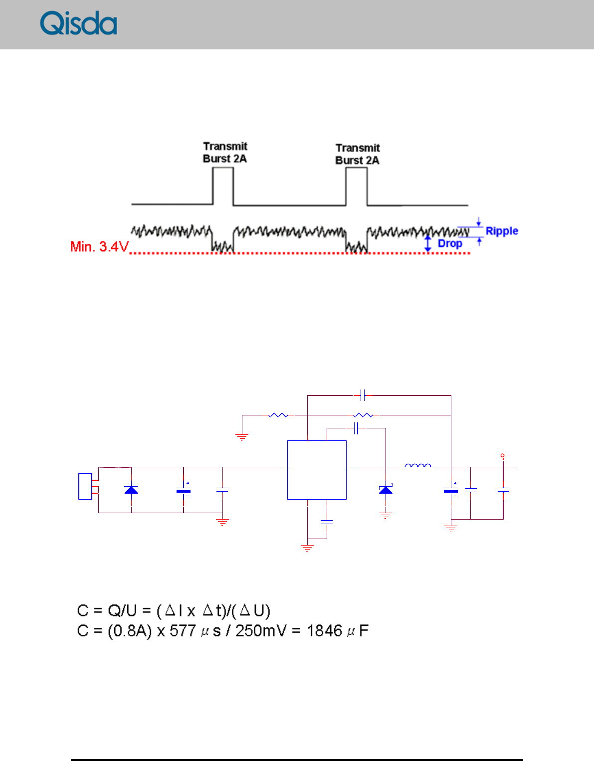
7.1 Power
The operating voltage of M66 is between 3.3V and 4.7V. Please make sure that the supply
voltage is still in the proper range when a maximum current is drawn from the power supplu
when a maximum RF output power is required.
Please note that once the supply voltage to M66 drops below 3.3V, module would be shut
down. If a power supply regulator is used for VBAT (power supply to M66), please make sure
the maximum output current rating should be more than 2A which is the minimum
requirement for a maximum RF output power. A reference design for a switching power
supply is shown below. The voltage rating of C31 and C35 should be raised higher if Vin is
greater than 12V. LM2676S-ADJ (or LM2673S-ADJ) can be used as the switching regulator in
the reference design.
C58 6.8N
1 2
VBAT
L6
33uH/3A
R27 1K 1% R28 2.49K 1%
C30 10nF/50V
C36
3.3nF
D5
RB051L-40
1 2
C34
0.1UF
C51
100pF
12
U3
LM2676S-ADJ
GND
4
Vout 1
Vin
2
ON//OFF
7
FB 6
CB 3
C31
100uF/16V
C35
0.47uF/16V
VBAT
D4
S3J
1 2
J6
CON3-9V
1
2
3
C33
330uF/10V
TO-263
Vbatt=Vfb*(1+R27/R28)=4.21V
Vfb=1.21V
A large capacitor with low ESR or parallel capacitors can be used to compensate the
insufficient supply current provided by the power regulator. The required capacitance can be
calculated from the following equations.
C = Capacitance in μF
Δt = GSM time slot (577 μs)
Q = Electricity charger
ΔU = Voltage drop
ΔI = Compensation in current (the required current – the supplied current)
Version: 0.0.1 - 22 - 2011/6/10
M66 Design Guide
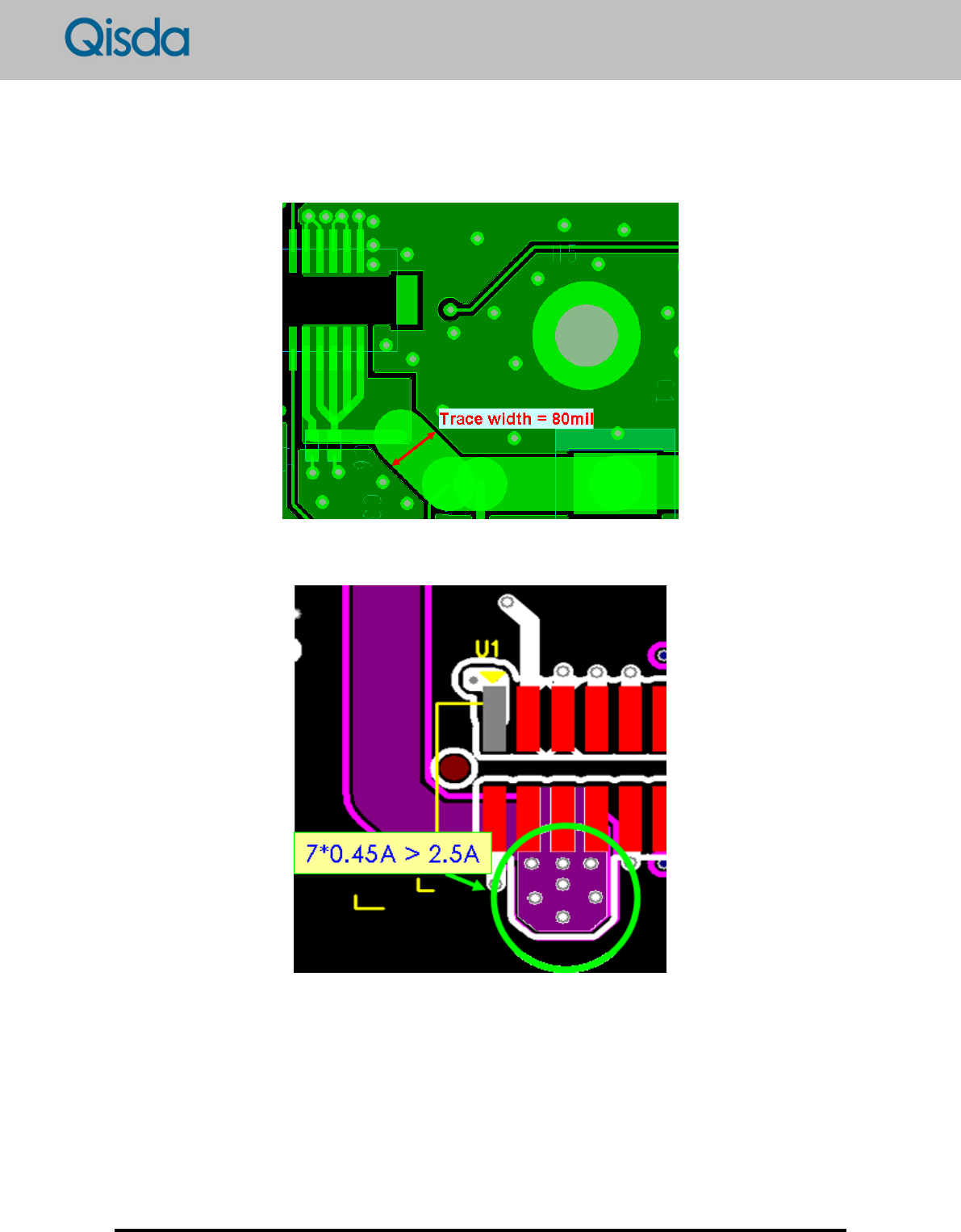
During power layout design, there are 2 reminders
A. Width
A.1 VBAT width: at least 80mil.
B. Recommend to have at least 7 via holes if VBAT needs to go through different layers to
have a minimum resistance.
Version: 0.0.1 - 23 - 2011/6/10
M66 Design Guide
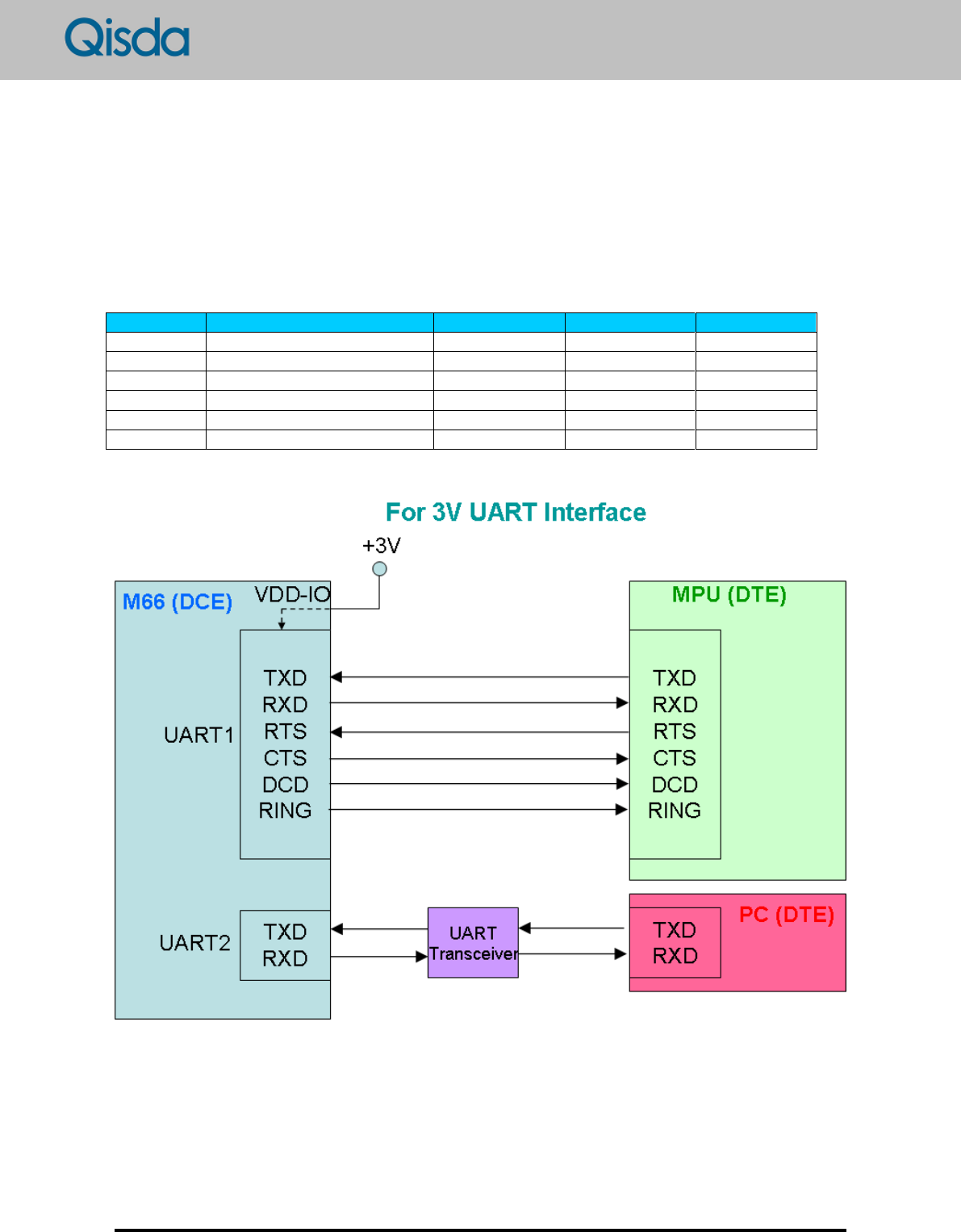
7.2 UART
The serial interface UART1 supports 6-wired, 4-wired, or 2-wired interface. M66
communicates with an external MPU via UART1. The factory default baud rate of UART1 is
9600 and it supports auto baud rate.
The main function of UART2 is for debug. It communicates with PC via UART
transceiver.
M66 serves as a DCE and the UART pin definition is as the following table.
RS232 pin
Name
Direction
M66 pin name
M66 pin no.
3
Transmit Data (TXD)
DTE M66
TXD
17
2
Receive Data (RXD)
DTE M66
RXD
15
7
Request To Send (RTS)
DTE M66
RTS
34
8
Clear To Send (CTS)
DTE M66
CTS
37
1
Data Carrier Detect (DCD)
DTE M66
DCD
39
9
Ring Indicator (RI)
DTE M66
RI
32
It is recommended to use 3V interface.
Version: 0.0.1 - 24 - 2011/6/10
M66 Design Guide
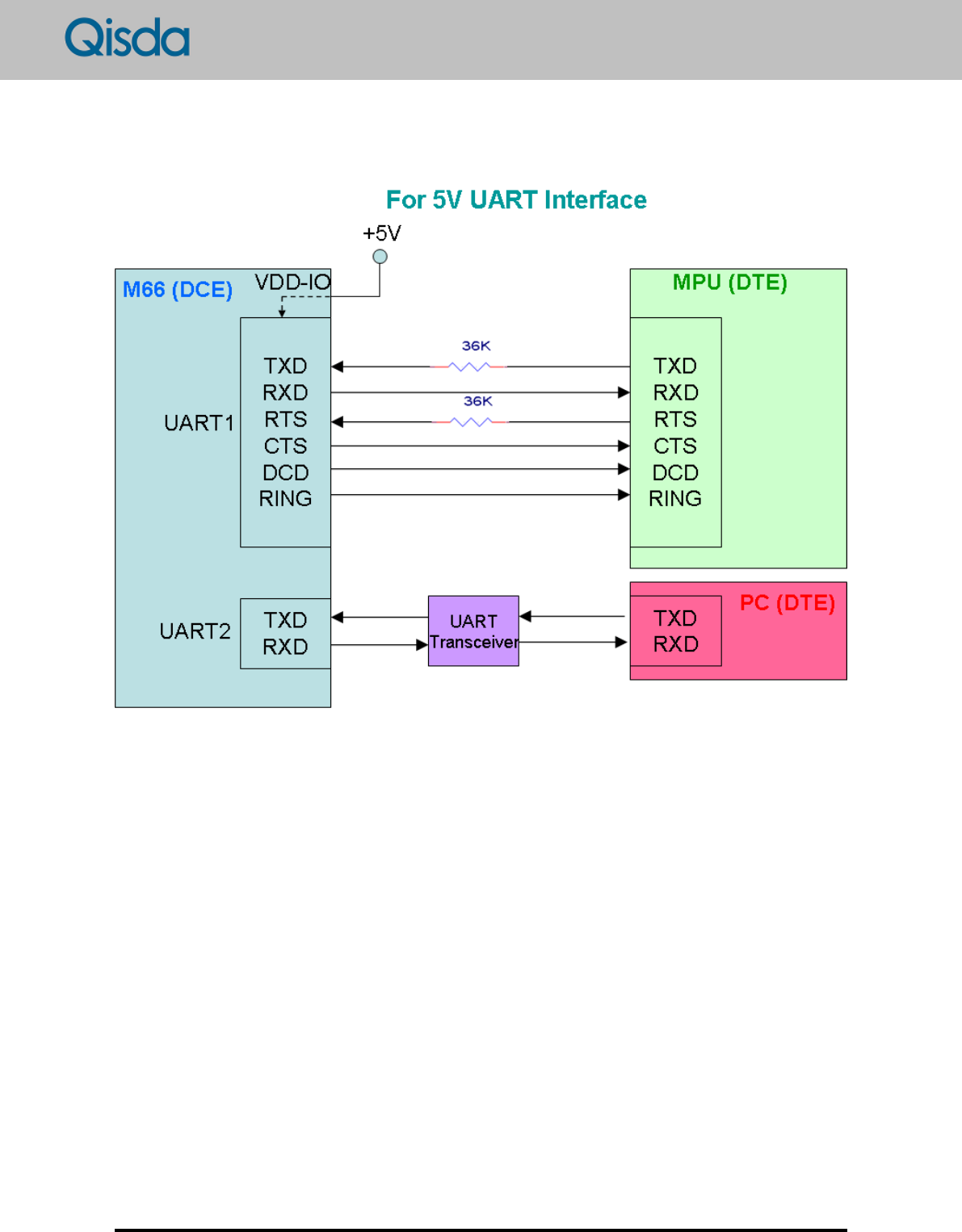
A level shift circuit should be added to the system if the UART interface of host side is not
3V. The following is an example of 5V interface.
Version: 0.0.1 - 25 - 2011/6/10
M66 Design Guide
7.3 Audio
It divides into 2 parts, microphone (uplink) and receiver/speaker (downlink).
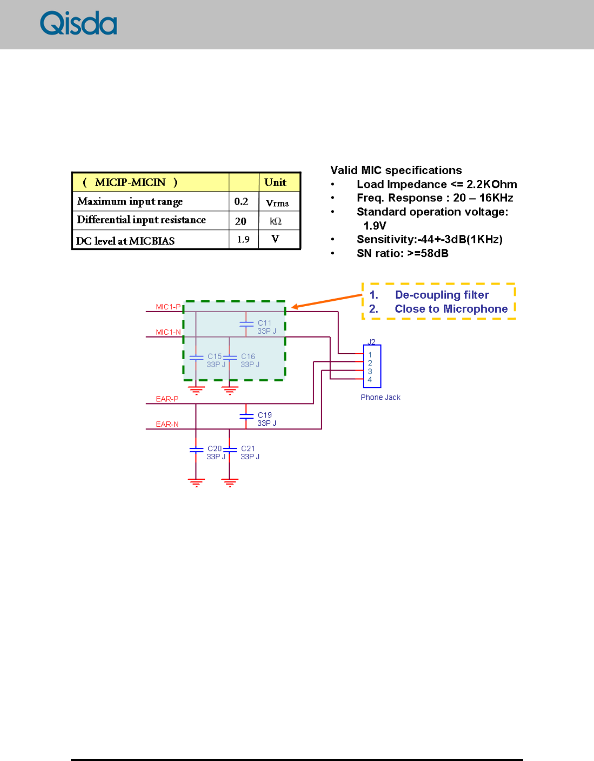
7.3.1 Microphone
Microphone schematics design is shown below for reference:
1. Please use the differential circuit design.
2. The microphone signal traces should be as short as possible.
3. Add decoupling circuits for external microphone bias and audio power supply to reduce
TDD noise.
4. Audio traces should be kept away from the VBATT and high speed clock traces.
5. Good shielding for audio path including components and traces. If possible, use via holes
to connect the ground shielding above and beneath the audio signals.
6. Twisted pair for external microphone lines. No necessary to use copper foil to wrap
around external microphone lines.
7. The distance between microphone and antenna should be at least 10 cm.
8. Add the small capacitor (33pF) across the microphone input traces to suppress the noise.
Version: 0.0.1 - 26 - 2011/6/10
M66 Design Guide
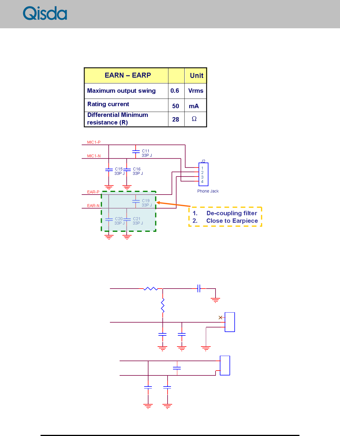
7.3.2 Receiver/Speaker
Receiver/speaker schematics design is shown below for reference:
As to the Hands-free application, it is suggested to use MIC2/MICBIAS and SPK-P/SPK-N to
get a better audio performance. SPK-P/SPK-N could drive a 8Ω speaker directly without an
external audio amplifier and the output power is 500 mW.
J3
CON3
1
2
3
C22 2.2U 6.3VR17
220
R18
2.2K J
MICBIAS
MIC2
C27
33P J C28
1000P K
C31
33P J C32
33P J
SPK-P
C30
33P J
SPK-N
J4
CON2
1
1
2
2
Version: 0.0.1 - 27 - 2011/6/10
M66 Design Guide
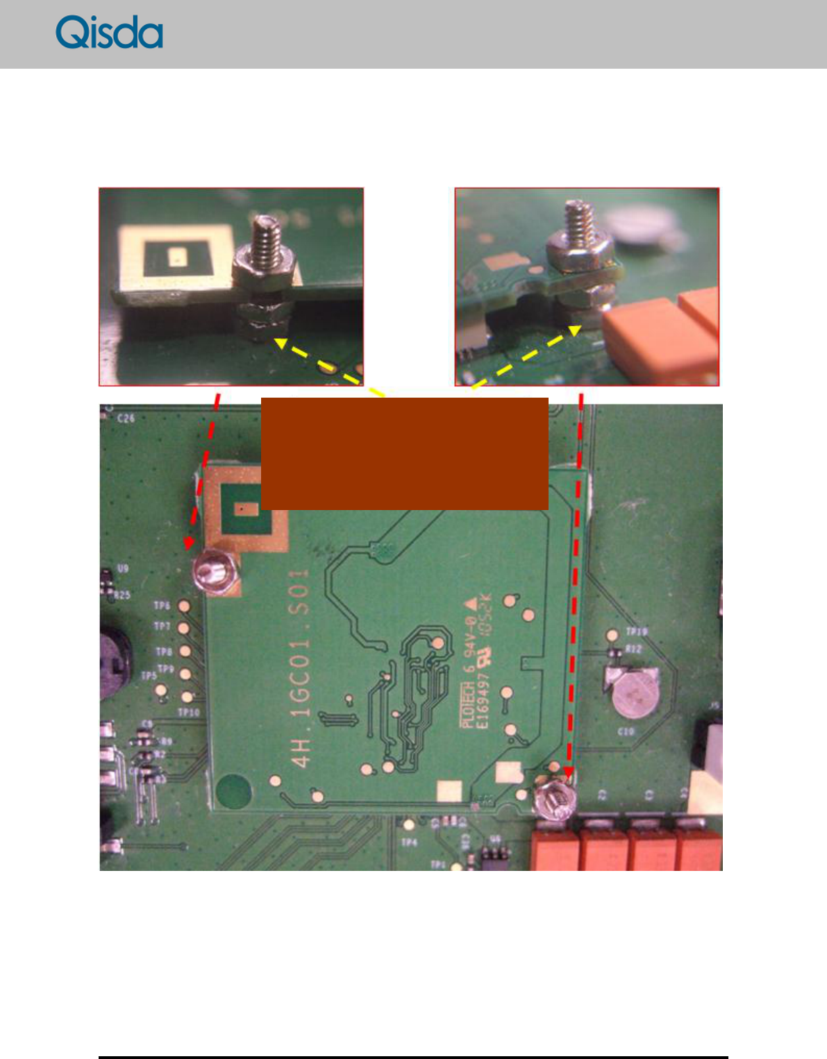
7.3.3 Grounding and Layout
Good grounding and conductive screws/screw holes are important to the audio quality and
performance. Please take special attention to the PCB layout of the screw holes and the
surrounding ring area. They should be copper plated and electrically conductive.
Tighten the screws which should
be electrical conductive.
The screw holes and surrounding
pad area should be conductive.
Version: 0.0.1 - 28 - 2011/6/10
M66 Design Guide
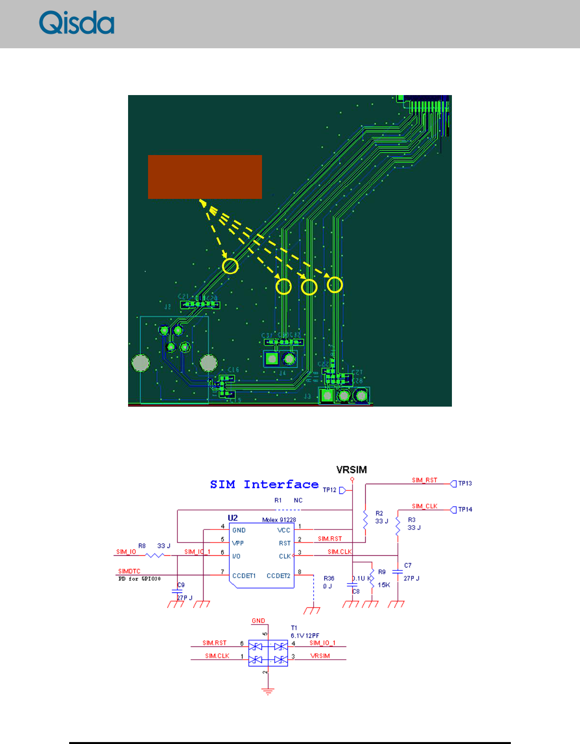
Recommended audio trace layout is illustrated in the following diagram.
7.4 SIM
The Vpp pin (Programming Voltage) is no function in current plug-in SIM. Please leave it
opened. The reference circuit is depicted below.
Balanced circuit
Version: 0.0.1 - 29 - 2011/6/10
M66 Design Guide
7.4.1 ESD
7.4.1.1 ESD protection diodes
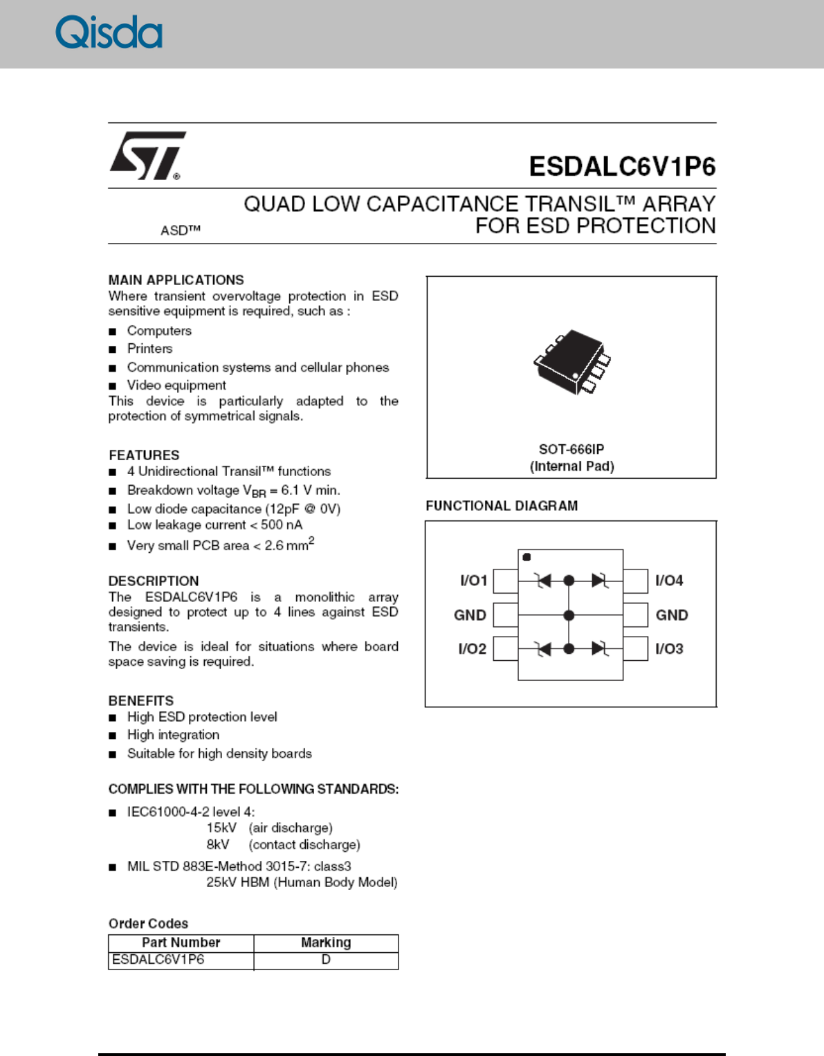
An ESD protection circuit could prevent the SIM cards from being damaged by ESD. Please
add an ESD circuit close to the CIM circuit to prevent ESD damaged. It is suggested to use
the following EDS protection diode.
Version: 0.0.1 - 30 - 2011/6/10
M66 Design Guide
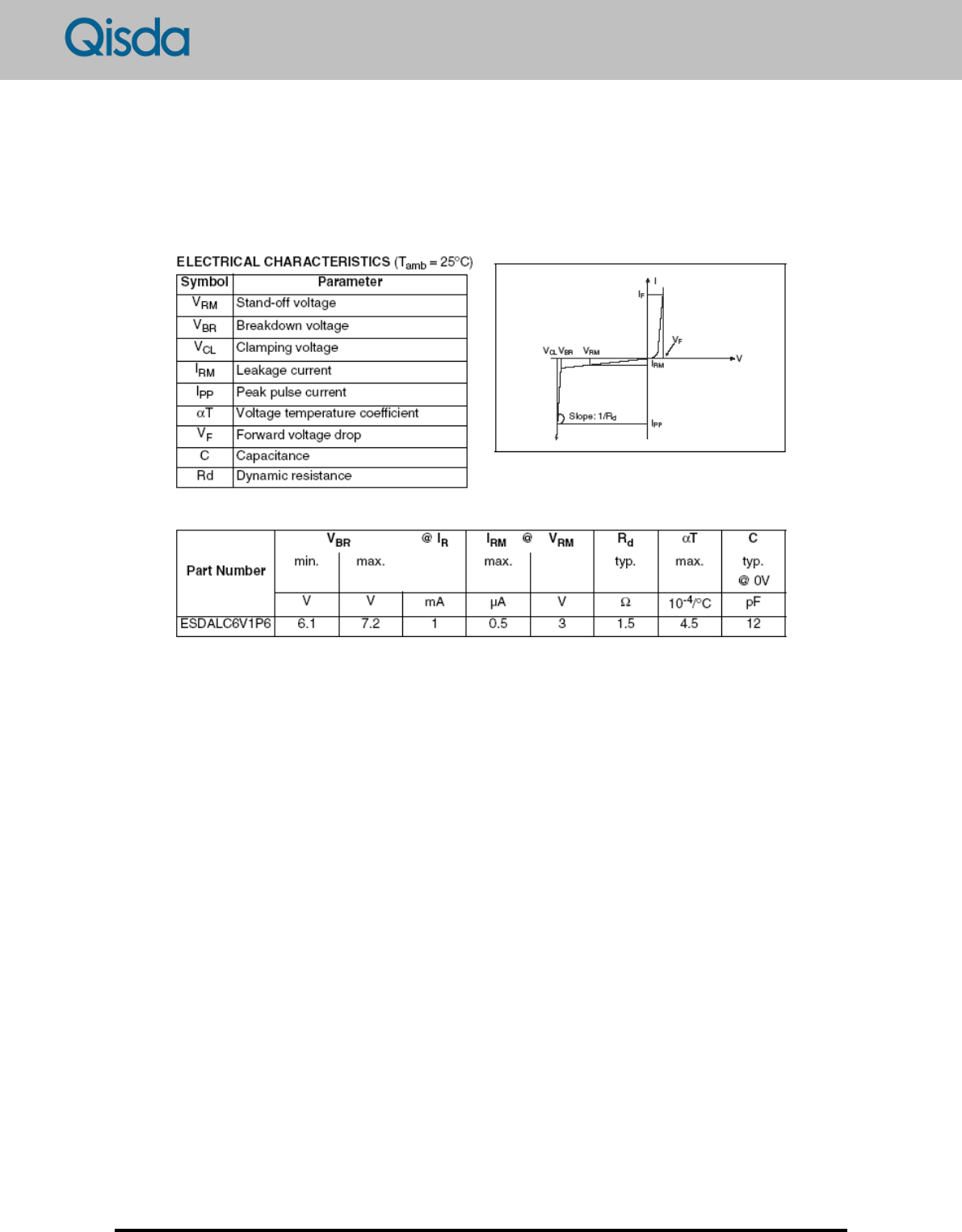
Electrical characteristics of the ESD protection diodes are shown as below for reference.
Version: 0.0.1 - 31 - 2011/6/10
M66 Design Guide
Recommended ESD protection components from different vendors:
SESMF05C
SENZQA5V6AV5
SEDF6A6V8
AMOTECH
AVSC 5S 04F 025
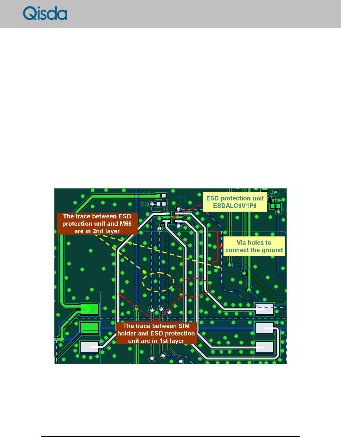
7.4.1.2 SIM holder
Besides ESD protection, the placement and layout of the SIM holder is also important to SIM
protection.
1. The ESD protection unit should be placed close to the SIM holder.
2. The ground pin of ESD protection unit should be directly connected to main ground. It will
make the ESD energy discharged to ground plane.
3. The trace width should be at least 0.3mm between SIM holder and ESD protection unit.
4. The ESD protection unit should be between SIM holder and M66.
5. The trace between ESD protection unit and M66 should be in a different layer and the width
should be at least 0.1mm.
Version: 0.0.1 - 32 - 2011/6/10
M66 Design Guide
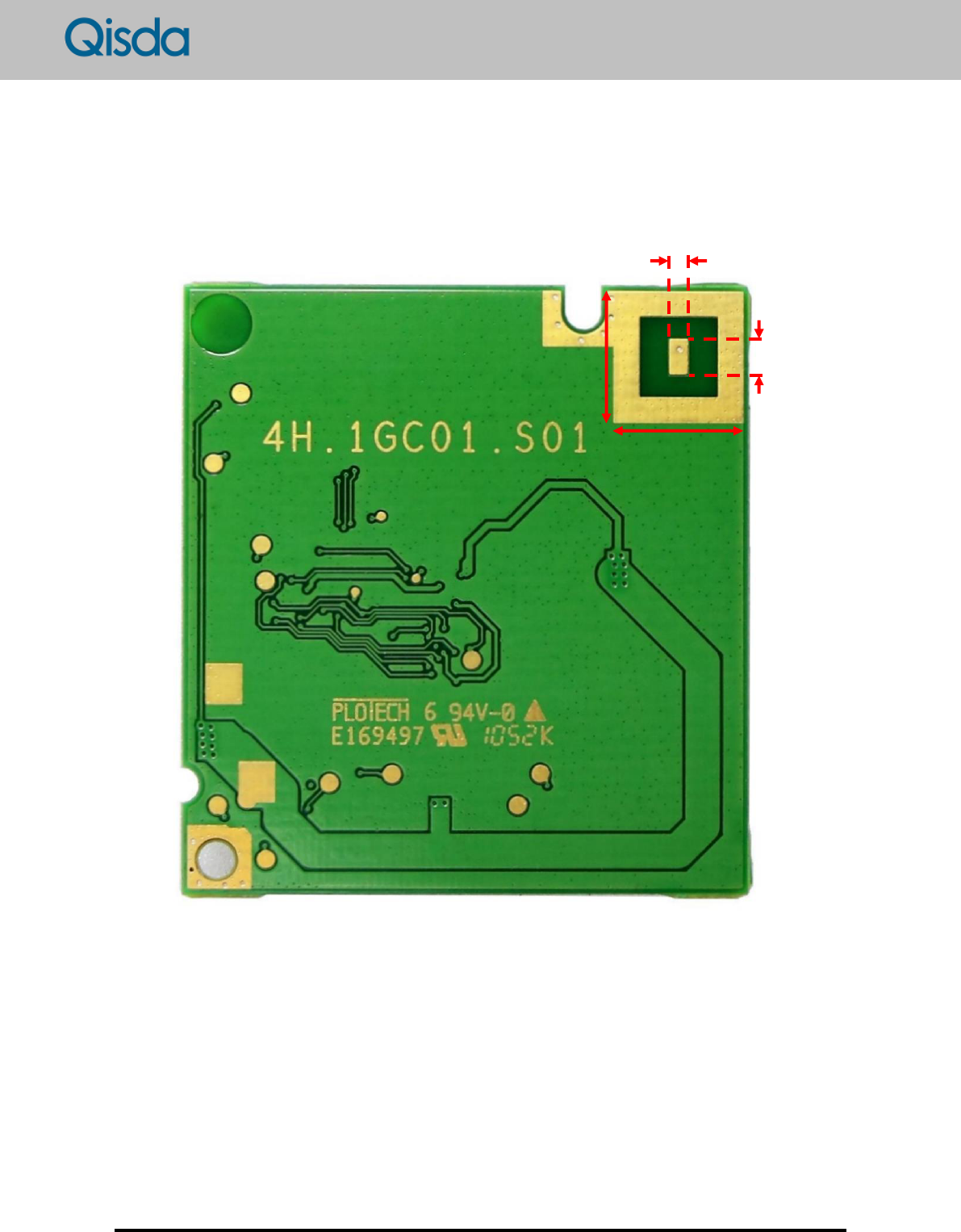
7.5 Antenna
M66 has an antenna pad on the BOTTOM side. It is possible to solder the coaxial cable
directly. The impedance of the cable should be 50 ohm (±10%)
M66 antenna pad
1mm
2mm
7.5mm
7.5mm
Version: 0.0.1 - 33 - 2011/6/10
M66 Design Guide
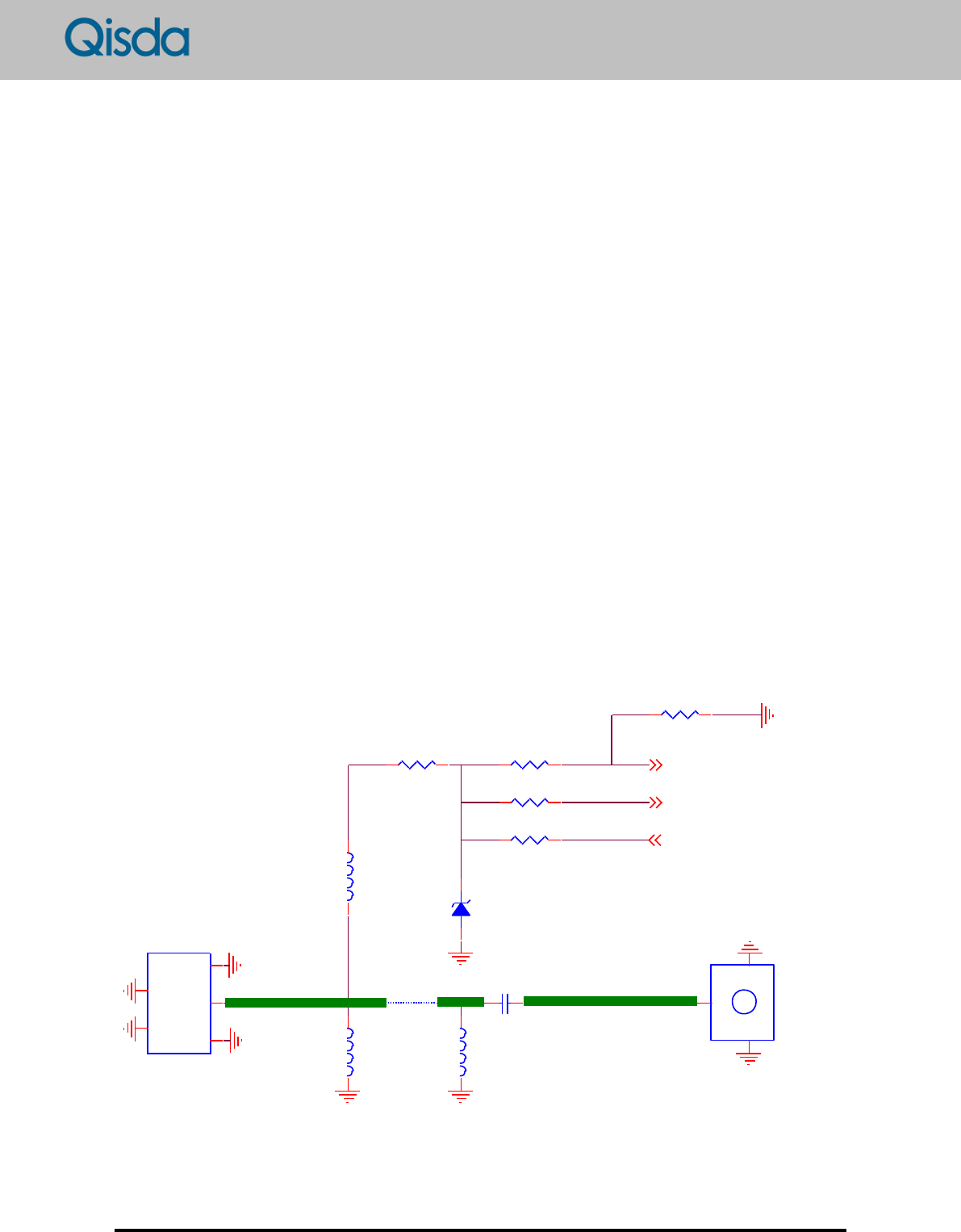
7.6 Antenna status detection application
Being able to detect and diagnose the antenna is a valuable feature for many system
integrators, and especially for automotive applications. The ability to detect whether the
antenna is connected to the communication appliance is useful for diagnosing installation
or production problems as well as any tampering with the system. Users can detect the
connection status by AT command. The responses are three kinds of status:
1. Antenna is connected to the RF cable properly.
2. The signal line of antenna is disconnected from RF Cable.
3. The signal line of antenna is connected to GND by accident.
If the signal line of antenna is short circuited to the +36V Power line ,(Ex. The
battery in automobile), M66 will inform MPU of emergency status by ANT_EMG pin.
Application Reference Circuitry is shown below. The following assumes that the
application is using a commonly found 10KΩ DC terminated antenna. The green bold line
is micro-strip line with 50Ω characteristic impedance. PAD1 is the RF connector for
Antenna.
Ant_Dect_EN 2
Ant_Dect_ADC 2
R32 0 J
ZD1
MM5Z3V0
A K
J8
2K90002003
1
1
22
3
3
PAD1
ANT-PAD
A1
GND 2
GND
3
GND
4
GND 5
C40
47P F
R30
15K F
L4
NC
R31
68K F
R27
18K F
L3
NC
L2
18NH J
R28
8.2K F
R29
15K F
VIO_3V3 2,3