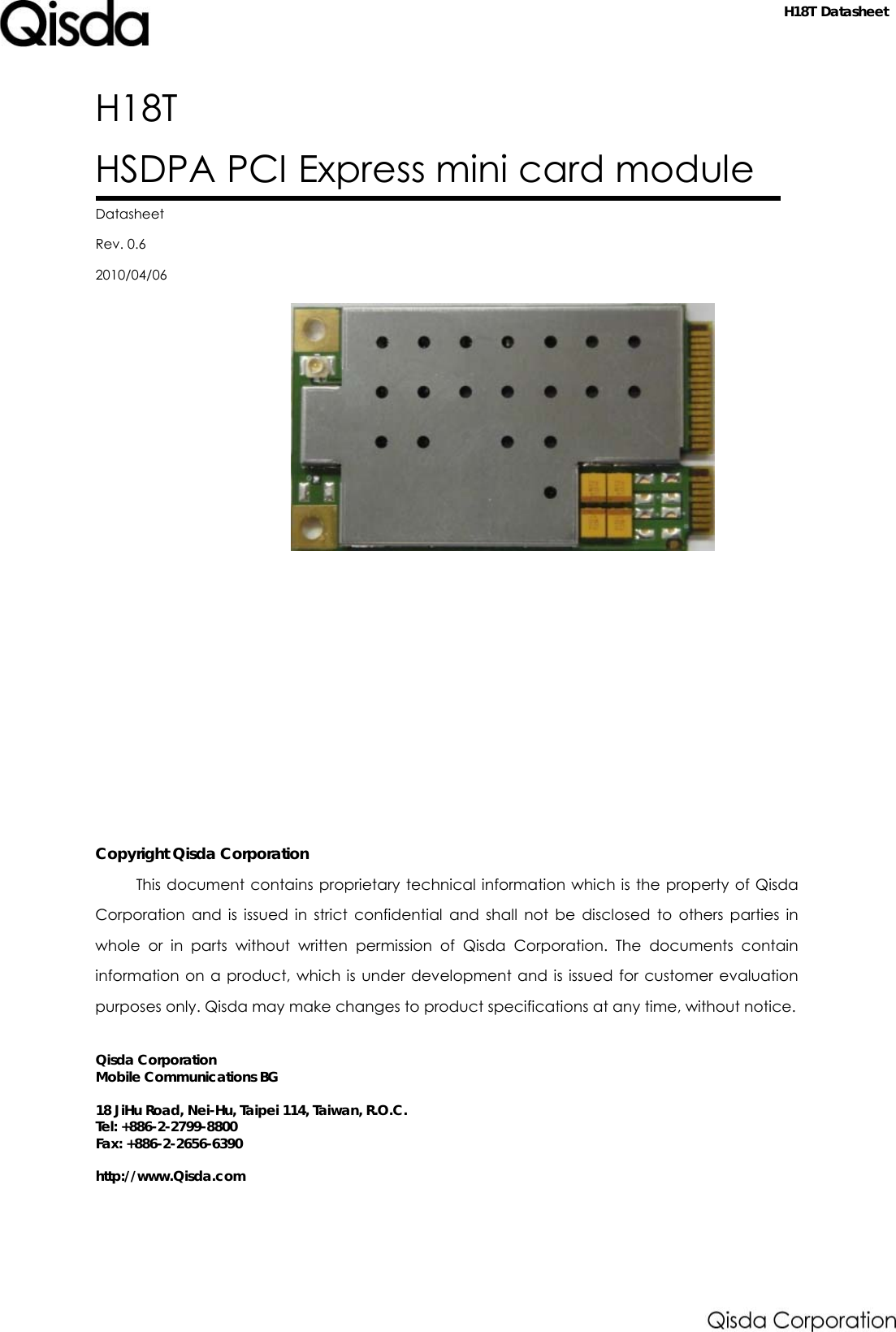
Qisda H18T HSDPA PCI EXPRESS MINI CARD MODULE User Manual H18T 2010 04 06
Qisda Corporation HSDPA PCI EXPRESS MINI CARD MODULE H18T 2010 04 06
UserManual.wiki
>
Qisda
>
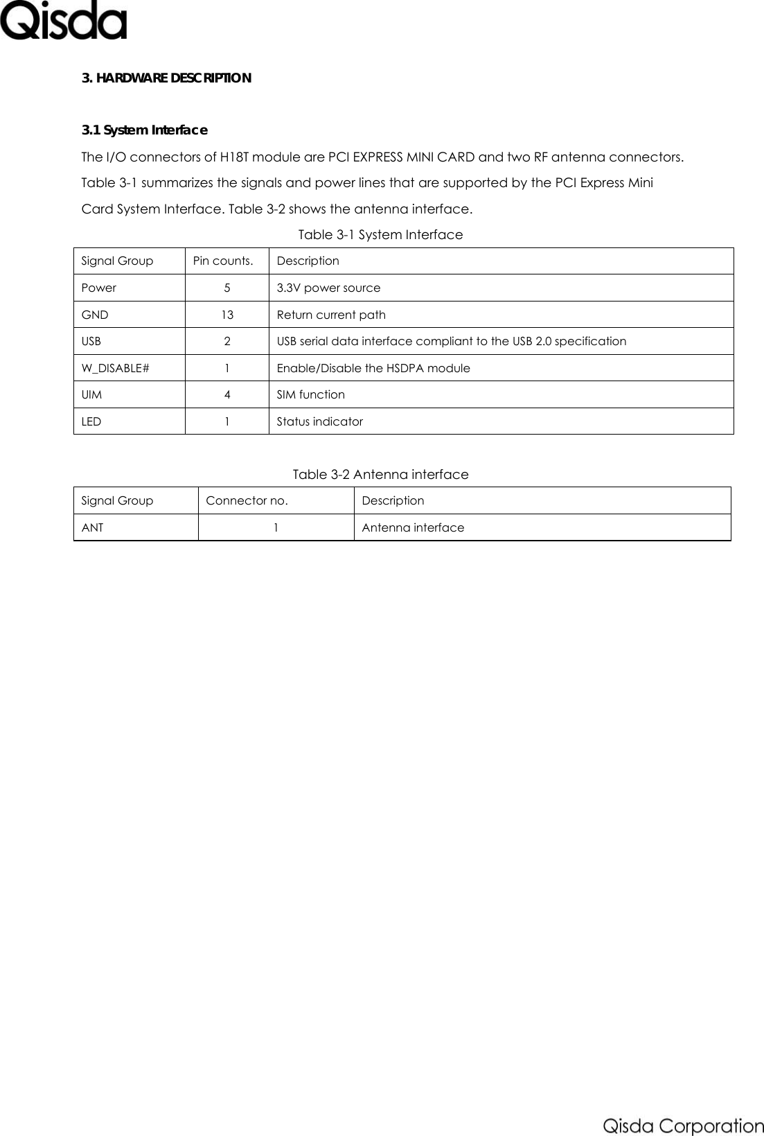
H18T User Manual
Users Manual
Navigation menu
Upload a User Manual
Namespaces
Wiki Guide
HTML
PDF
Info
Views
User Manual
Discussion / Help
Navigation