Quanta Computer 1KU3 1KU3 User Manual 1KU product spec
Quanta Computer Inc 1KU3 1KU product spec
manual

___________________________________________________________
UANTA COMPUTER INC.
___________________________________________________________
1KU3 Product Specification
Nov. 28th, 2011 Revision: 2B
Issued By: Suya Hou
Checked By: Claire Huang
___________________________________________________________________________
The release of this document is under controlled by the company. Any extra copy of this
document must be written permission by the project manager.
___________________________________________________________________________
- Quanta Confidential -

UANTA COMPUTER INC. CNBU/1KU3
________________________________________________________________________________________
____________________________________________________________________________
1KU Product Specification Rev. 2B Page: 2
- Quanta Confidential -
Document History:
Vision
Release By
Date
Note
2A
Suya Hou
2011.11.25
First release
2B
Suya Hou
2011.11.28
Add CE statement

UANTA COMPUTER INC. CNBU/1KU3
________________________________________________________________________________________
____________________________________________________________________________
1KU Product Specification Rev. 2B Page: 3
- Quanta Confidential -
CONTENT
1. INTRODUCTION ...................................................................................... 4
1.1 RADIO FREQUENCY CONFIGURATIONS ....................................................................................... 4
2. MAIN FEATURES ..................................................................................... 4
3. MECHANICAL SPECIFICATIONS................................................................ 7
4. PERFORMANCE ....................................................................................... 7
4.1 RF SPECIFICATION ................................................................................................................. 7
4.2 ELECTRICAL SPECIFICATION ..................................................................................................... 8
4.2.1 Power Specification............................................................................................................................. 8
4.2.2 Pin Assignment .................................................................................................................................... 8
5. AT COMMAND ....................................................................................... 10
5.1 3GPP STANDARD AT COMMANDS......................................................................................... 10
6. FCC ........................................................................................................ 10
FCC ID: HFS1KU3 .................................................................................................................. 10
7. CE MARKING ......................................................................................... 10
UANTA COMPUTER INC. CNBU/1KU3
________________________________________________________________________________________
____________________________________________________________________________
1KU Product Specification Rev. 2B Page: 4
- Quanta Confidential -
1. Introduction
1KUx is a customized PCI Express Mini Card, which is developed on Qualcomm MDM9600/9200 platform
and capable to provide various frequency configurations, support data operation on LTE, EVDO, HSUPA, HSDPA
and WCDMA connectivity for portable and hand-held computers.
1.1 Radio Frequency Configurations
The required radio frequency has been defined into 3 SKUs based on customer needs, 1KUx is a general
definition of this embed module, precise name will be named as 1KU1, 1KU2 and 1KU3 in accordance with
bands configuration.
Due to limited space reserved for the module and Qualcomm’s chipset configuration, 3 SKUs have to be
realized by leveraging 2 PCBs design. This PCI Express Mini Card is able to support UP TO Quad Bands in
LTE/UMTS and Quad Bands in EDGE, GPRS, and GSM if required. Hence, the following SKU table will become as
whole framework of product specification.
Table 1-1
Quanta Model
Name
1KU1
1KU2
1KU3
QCI P/N
211KUMB0070
211KUMB0050
211KUMB0060
Description
LTE & CDMA
HSPA+ Only
LTE & HSPA+
HSPA+
X
850/900/1900/2100/AWS
850/1900/2100
LTE
700U
X
AWS/700D
EVDO
800/ 1900 MHz
X
X
PCB Design
PCB-1
PCB-2
PCB-2
2. Main Features
The following features set can be referred to 1KU1, 1KU2 and 1KU3, bands supported frequency depend on
each SKU bands configuration.
Features
Items
Descriptions
Remarks
Physical
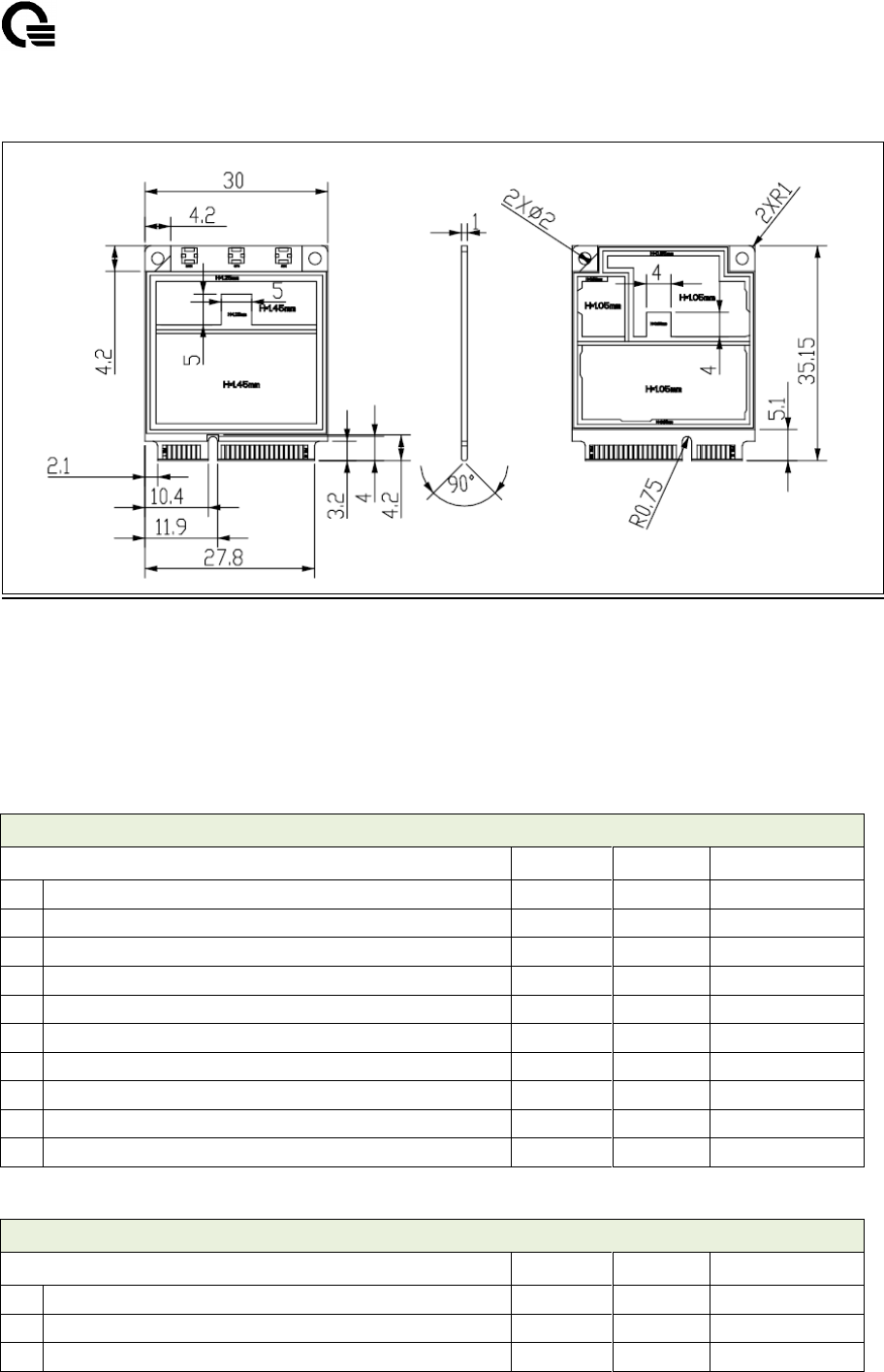
Outlook
Dimension
35.18 x 30 x 4mm
Weight
9 g
Temperature
Range
Operation
Temperature
-10°C to +55°C
Storage
Temperature
-20°C to +80°C
DC Power
Supply
Supply Voltage
3.4~4.2V
Interface
Edge connector
- 52 pins
- 0.8 pitch
- 0.5A rating current
Host
communication
Alternative:
- USB 2.0
- 8 bit SDIO at 1.8V

UANTA COMPUTER INC. CNBU/1KU3
________________________________________________________________________________________
____________________________________________________________________________
1KU Product Specification Rev. 2B Page: 5
- Quanta Confidential -
SIM
- (U)SIM 1.8V/3V
- Class B/Class C
Connection
2 Antenna W_FL connectors:
- 1 Primary for WCDMA/HSPA/LTE/Cdma2000/EVDO
- 1 auxiliary for HSPA/LTE/EVDO Rx diversity
Communication
ports at USB
- 1 Modem port
- 1 Diagnostic port
- 1 AT command port
- 1 NDIS interface
CPU
Baseband
Processor
Qualcomm MDM 9600/9200 600MHz
- Application μP: ARM926-256MHz
- SW/FW Processor: QDSP6 at up to 595 MHz
PMIC
PMIC 8028
Internal
Memory
- 64 MB DDR SDRAM internal stacked memory
- 166 MHz maximum speed
- 32-bit data width support
- 1.8 V interface
External
Memory
NAND Flash
- 1Gb
- 63-Ball FBGA (9 x 11 x 1.0 mm)
- Operating voltage: 1.8V
- Memory Density: 128M x 8 bit
Radio
UMTS
Frequency
- B1: UMTS-2100 (1920-1980MHz; 2110-2170MHz)
- B2: UMTS-1900 (1850-1910MHz; 1930-1990MHz)
- B4: UMTS-AWS (1710-1755MHz; 2110-2155MHz)
- B8: UMTS-900 (880-915MHz; 925-960MHz)
- B5: UMTS-850 (824-849MHz; 869-894MHz)
Details refer to SKUs
table
EVDO
Frequency
- BC0:EVDO-800 (824-849MHz; 869-894MHz)
- BC1:EVDO-1900(1850-1910MHz; 1930-1990MHz)
Only request in SKU1
LTE
Frequency
- B13-700U (777-787MHz; 746-756MHz)
- B17-700D (704-716MHz; 734-746MHz)
- B4-AWS (1710-1755MHz;2110-2155MHz)
UNABLE to support all
LTE bands in one SKU
RF System
RTR8600
- UMTS/HSDPA/HSUPA 850/900/1900/2100/AWS
Power class 3 (+24dBm)
- LTE
Power class 3 (+23 dBm)
- CDMA/EVDO
Power class 3(BC0/+23dBm)
Power class 2(BC1/+23dBm)
Rx Diversity
Will differ according to each SKU:
- EVDO 800/1900MHz
- LTE 700U/700D/AWS
- UMTS 850/900/1900/AWS/2100
Air Interface
Features
UMTS Rel.99
- Division Duplex: FDD
- Peak PS data rate: 384 kbps UL/ 384 kbps DL

UANTA COMPUTER INC. CNBU/1KU3
________________________________________________________________________________________
____________________________________________________________________________
1KU Product Specification Rev. 2B Page: 6
- Quanta Confidential -
HSDPA
- Modulation: QPSK/ 16QAM
- Support Category 6/8;
- 7.2 Mbps/DL (Standalone);
HSUPA
- Modulation: QPSK/ 16QAM
- Support Category 5/6 (2msec TTI)*
- Up to 5.76 Mbps/UL (Standalone)
HSPA+
- Rel 8 DL *
Dual carrier with 64 QAM, for up to 42 Mb/s
support
2 × 2 MIMO with 64 QAM, for up to 42 Mb/s
support
- Rel7 DL
64 QAM, for up to 21 Mb/s support
2 × 2 MIMO with 16 QAM, for up to 28 Mb/s
support
- Up to 11.4Mbps/UL
*:
--Depends on
Qualcomm support
plan
--Cat. 24 only support
in 1KU2.
LTE Rel 8
- 100 Mbps DL/50 Mbps UL (Cat 3, 10MHz)
- 1.4 to 20 MHz RF bandwidth
- 2 × 2 downlink SU-MIMO
CDMA 1xEV-DO
Rev B
- 3.1Mbps DL/1.8 Mbps UL (Rev A)
- 14.7 Mbps DL/5.4 Mbps UL (Rev B)*
- Combines up to three carriers from within 10 MHz
RF bandwidth
*Rev B have not
supported in
Qualcomm SW drop
yet
Data Service
Data Mode
- CSD Rate Up to 9.6, 14.4 and 64kbps
- DTE/DCE interface via USB 2.0 full speed
- 3GPP 27.007 AT Command Set
- 3GPP 27.005 Short Message
UANTA COMPUTER INC. CNBU/1KU3
________________________________________________________________________________________
____________________________________________________________________________
1KU Product Specification Rev. 2B Page: 7
- Quanta Confidential -
3. Mechanical Specifications
4. Performance
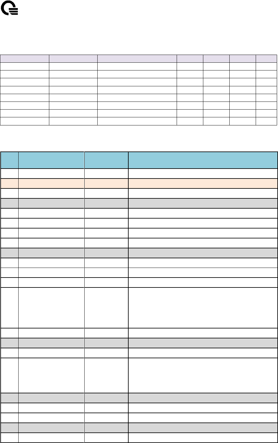
4.1 RF Specification
Condition:
Voltage @3.4 V and Temperatures: 25゚C
Rx Conductive Sensitivity
Band
Typ.
Max
Unit
1
UMTS-850, 12.2 kbps, 0.1%
-109
-104.7
dBm
2
UMTS-900, 12.2 kbps, 0.1%
-106*
-103.7
dBm
3
UMTS-AWS, 12.2 kbps, 0.1%
-108*
-106.7
dBm
4
UMTS-1900, 12.2 kbps, 0.1%
-107
-104.7
dBm
5
UMTS-2100, 12.2 kbps, 0.1%
-109
-106.7
dBm
6
CDMA2000-BC0(800MHz),FER<0.5%
-107
-104
dBm
7
CDMA2000-BC1(1900MHz),FER<0.5%
-107
-104
dBm
8
LTE-700U,QPSK,5MHz,>95%
-100
-97
dBm
9
LTE-700D, QPSK,5MHz,>95%
-100*
-97
dBm
10
LTE-AWS, QPSK, 5MHz,>95%
-103*
-98
dBm
*: These will be adjusted further.
Tx Conductive Power
Band
Typ
Min
Unit
1
UMTS850/900/1900/2100/AWS
23
21
dBm
2
CDMA2000
24
23
dBm
3
LTE, Class3
23
21
dBm
UANTA COMPUTER INC. CNBU/1KU3
________________________________________________________________________________________
____________________________________________________________________________
1KU Product Specification Rev. 2B Page: 8
- Quanta Confidential -
4.2 Electrical Specification
4.2.1 Power Specification
Name
Pin
Description
Min
Typ
Max
Unit
VCC_VBAT
2, 24, 39, 41, 52
VCC power
3.4
3.8
4.2
V
VCC_USIM/ 3.0V
8
USIM power output 3.0V
2.7
3
3.3
V
VCC_USIM/ 1.8V
8
USIM power output 1.8V
1.62
1.8
1.98
V
V_IH
1.8V Digital I/O
input high voltage
1.62
1.8
1.98
V
V_IL
1.8V Digital I/O
input low voltage
0
0.1
0.45
V
V_OH
1.8V Digital I/O
output high voltage
1.62
1.8
1.98
V
V_OL
1.8V Digital I/O
output low voltage
0
0.1
0.45
V
PERST_N
22
Hardware Reset (PU)
-0.3
0
0.6
V
4.2.2 Pin Assignment
Pin
Name
Power Level
Description
1
POWER_ON_OFF
1.8V
Modem power on/off
2
VCC_VBAT
4.2~3.4V
Supply voltage for Modem
3
VREG_MSME_1V8
1.8V
Supply voltage for JTAG function
4
GND
GND
5
MDM_JTAG_PS_HOLD
JTAG Function
6
WAKE_UP
1.8V
Wake-up Modem
7
MDM_JTAG_RESET_N
JTAG Function
8
VREG_RUIM1
1.8/3V
SIM function
9
GND
GND
10
UIM1_DATA
SIM function
11
PA_state
1.8V
Indicate 3G/LTE/EVDO PA state for coexistence
12
UIM1_CLK
SIM function
13
(1)MDM_RTCK
or
(2)TCXO_GPS_EN
(1)JTAG Function
or
(2)Enable the output of TCXO(19.2MHz) so as to be used
by GPS of main system
*Depends on system how to design
14
UIM1_RESET
SIM function
15
GND
GND
16
UIM1_DET
Detection of SIM insertion/plug-out
17
(1)MDM_TCK
or
(2)TCXO_GPS
(1)JTAG Function
or
(2)TCXO(19.2MHz) output for GPS of main system
*Depends on system how to design
18
GND
GND
19
MDM_TMS
JTAG Function
20
Suspend
1.8V
Trigger Modem to enter into sleep mode
21
GND
GND
22
PM28_RESET_N
Reset Modem

UANTA COMPUTER INC. CNBU/1KU3
________________________________________________________________________________________
____________________________________________________________________________
1KU Product Specification Rev. 2B Page: 9
- Quanta Confidential -
23
MDM_TDI
JTAG Function
24
VCC_VBAT
Supply voltage of Modem
25
MDM_TDO
JTAG Function
26
GND
GND
27
GND
GND
28
SDC2_MDM_CLK
SDIO CLK
29
GND
GND
30
SDC2_MDM_CMD
SDIO CMD
31
MDM_TRST_N
JTAG Function
32
SDC2_MDM_D0
1.8V
SDIO I/O interface
33
VBUS
Supply voltage of USB(for R&D USB debug port)
34
GND
GND
35
GND
GND
36
USB_D-
USB_D-
37
GND
GND
38
USB_D+
USB_D+
39
VCC_VBAT
Supply voltage of Modem
40
GND
GND
41
VCC_VBAT
Supply voltage of Modem
42
(WWAN_LED)
Indicate WWAN state for controlling LED of main system
43
GND
GND
44
SDC2_MDM_D1
1.8V
SDIO I/O interface
45
SDC2_MDM_D4
1.8V
SDIO I/O interface
46
SDC2_MDM_D2
1.8V
SDIO I/O interface
47
SDC2_MDM_D5
1.8V
SDIO I/O interface
48
SDC2_MDM_D3
1.8V
SDIO I/O interface
49
SDC2_MDM_D6
1.8V
SDIO I/O interface
50
GND
GND
51
SDC2_MDM_D7
1.8V
SDIO I/O interface
52
VCC_VBAT
Supply voltage of Modem

UANTA COMPUTER INC. CNBU/1KU3
________________________________________________________________________________________
____________________________________________________________________________
1KU Product Specification Rev. 2B Page: 10
- Quanta Confidential -
5. AT Command
5.1 3GPP Standard AT Commands
1. AT command set for GSM Mobile Equipment (ME) can be downloaded from
http://www.3gpp.org/ftp/Specs/html-info/0707.htm .
2. AT command set for User Equipment (UE) can be downloaded from
http://www.3gpp.org/ftp/Specs/html-info/27007.htm .
6. FCC
FCC ID: HFS1KU3
This module is complied to FCC requirement, all integrators have to be aware of the following information.
FCC RF Radiation Exposure Statement:
This equipment complies with FCC radiation exposure limits set forth for an uncontrolled environment. This
equipment should be installed and operated with minimum distance 20cm between the radiator & your body.
This transmitter must not be co-located or operating in conjunction with any other antenna or transmitter.
This device complies with Part 15 of the FCC Rules Rules.
Operation is subject to the following two conditions :
1) This device may not cause harmful interference, and
2) This device must accept any interference received, including interference that may cause undesired
operation of the device.
Only those antennas with same type and lesser gain filed under this FCC ID number can be used with
this device.
The final system integrator must ensure there is no instruction provided in the user manual or customer
documentation indicating how to install or remove the transmitter.
Required end product labeling:
Any device incorporating this module must include an external, visible, permanent marking or label which
states “Contains FCC ID: HFS1KU3
7. CE Marking
This device has been tested to and conforms to the regulatory requirements of the European Union and has
attained CE Marking. The CE Mark is a conformity marking consisting of the letters “CE”. The CE Mark applies to
products regulated by certain European health, safety and environmental protection legislation. The CE Mark is
obligatory for products it applies to: the manufacturer affixes the marking in order to be allowed to sell his
product in the European market.
This product conforms to the essential requirements of the R&TTE directive 1999/5/EC in order to attain CE
Marking. A notified body has determined that this device has properly demonstrated that the requirements of
the directive have been met and has issued a favorable certificate of expert opinion. As such the device will
bear the notified body number 0560 after the CE mark
The CE Marking is not a quality mark. Foremost, it refers to the safety rather than to the quality of a product.
Secondly, CE Marking is mandatory for the product it applies to, whereas most quality markings are voluntary.
Marking: The product shall bear the CE mark, the notified body number(s) as depicted to the right. CE 0560.