Quanta Microsystems HM500 WHDI Transmitter Module User Manual AMN11100
Quanta Microsystems, Inc. WHDI Transmitter Module AMN11100
UserManual.wiki
>
Quanta Microsystems
>
HM500 User Manual
Manual
Navigation menu
Upload a User Manual
Namespaces
Wiki Guide
HTML
PDF
Info
Views
User Manual
Discussion / Help
Navigation
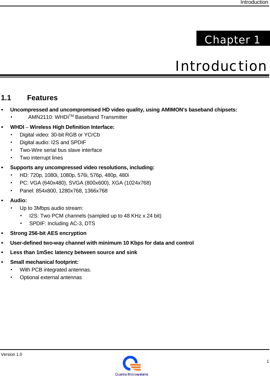
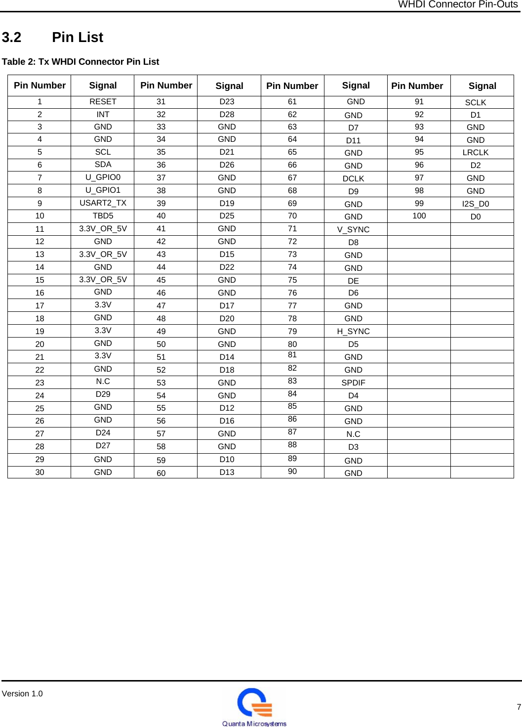
![WHDI Connector Pin-Outs Chapter 3 WHDI Connector Pin-Outs 3.1 Signals Table 1: WHDI Connector Signals # of Pins Pin Name Description/Functionality Group Direction Tx Remarks 30 D[29:0] 30-bit RGB (10:10:10) or YCrCb (10:10:10) Video In 1 DCLK Video data clock Video In Up to 78.125 MHz 1 DE Data enable Video In 1 H_SYNC Horizontal sync Video In 1 V_SYNC Vertical sync Video In 1 SPDIF SPDIF audio interface Audio In 1 SCLK I2S continuous serial clock Audio In Up to 3.072Mbps1 LRCLK I2S Word Select (Left/right clock) which defines also the sampling rate Audio In 1 SDA Two-wire Serial Bus Data (Slave Mode) Control I/O Control I/F for WHDI 1 SCL Two-wire Serial Bus Clock (Slave Mode) Control In Control I/F for WHDI 1 INT Interrupt from WHDI module Control Out 1 RESET Reset / Power-down line Control In 1 TBD5 TBD5 is reserved in HM500, HM501 as an option for external power rail to the on board uC TBD TBD 3 3.3V VCC Power Power 3 3.3V_OR_5V High Power rail pins,In HM500, HM501 connect these power rail pins to the 3.3V power rail. Power Power connect to 3.3V 46 GND Ground Power Power 1 I2S_D0 1 U_GPIO0 1 U_GPIO1 1 USART2_TX 2 N.C. reserved Version 1.0 6](https://usermanual.wiki/Quanta-Microsystems/HM500/User-Guide-957984-Page-8.png)