Quanta Microsystems HM500 WHDI Transmitter Module User Manual AMN11100
Quanta Microsystems, Inc. WHDI Transmitter Module AMN11100
Manual

HM500
Transmitter
Module Datasheet
Version 1.0
Quanta Microsystems, Inc.
Tel:+886-3- 3979000
Fax:+886-3-397990
5F, No.188, WenHwa 2nd RdKuei Shan Hsiang,
Taoyuan Shien, 333,Taiwan

Table of Contents
Table of Contents
Chapter 1, Introduction ................................................................................. 1
1.1 Features ......................................................................................................................................................... 1
Chapter 2, Overview ....................................................................................... 3
2.1 AMN2110 WHDI Baseband Transmitter...................................................................................................... 4
2.2 LPC2103 Mini-MAC µController .................................................................................................................. 4
2.3 MAX2828 5GHz (802.11a) Transceiver........................................................................................................ 5
2.4 Power Amplifier (PA) .................................................................................................................................... 5
2.5 Board Connector (WHDI
TM
Connector)....................................................................................................... 5
2.6 EEPROM......................................................................................................................................................... 5
2.7 40MHz Clock Gen.......................................................................................................................................... 5
Chapter 3, WHDI Connector Pin-Outs..............................................................6
3.1 Signals ........................................................................................................................................................... 6
3.2 Pin List ........................................................................................................................................................... 7
Chapter 4, Mechanical Dimensions.......... ..................................................... 8
Version 1.0
i

Introduction
Chapter 1
Introduction
1.1
Features
•
Uncompressed and uncompromised HD video quality, using AMIMON's baseband chipsets:
•
AMN2110: WHDI
TM
Baseband Transmitter
•
WHDI – Wireless High Definition Interface:
•
Digital video: 30-bit RGB or YCrCb
•
Digital audio: I2S and SPDIF
•
Two-Wire serial bus slave interface
•
Two interrupt lines
•
Supports any uncompressed video resolutions, including:
•
HD: 720p, 1080i, 1080p, 576i, 576p, 480p, 480i
•
PC: VGA (640x480), SVGA (800x600), XGA (1024x768)
•
Panel: 854x800, 1280x768, 1366x768
•
Audio:
•
Up to 3Mbps audio stream:
•
I2S: Two PCM channels (sampled up to 48 KHz x 24 bit)
•
SPDIF: Including AC-3, DTS
•
Strong 256-bit AES encryption
•
User-defined two-way channel with minimum 10 Kbps for data and control
•
Less than 1mSec latency between source and sink
•
Small mechanical footprint:
•
With PCB integrated antennas.
•
Optional external antennas
Version 1.0
1

Introduction
•
RF characteristics:
•
MIMO technology, using 5GHz unlicensed band, 18MHz bandwidth.
•
Coexists with 802.11a/n and 5.8GHz cordless devices.
•
Support for Automatic Transmission Power Control (ATPC).
•
No line of sight needed between transmitter and receiver. It has a range of over 30 meters, suitable for
almost any room.
•
14mW typical transmission power.
•
Maximum 45mW transmission power.
•
Power requirements:
•
3.3V (±5%), ~5.6W
•
Certification & Compliance:
•
This device complies with part 15 of the FCC Rules. Operation is subject to the following two conditions:
(1) This device may not cause harmful interference, and (2) this device must accept any
interference received, including interference that may cause undesired operation.
•
Any changes or modifications not expressly approved by Amimon for compliance could void the user's
authority to operate the equipment.
•
This equipment has been tested and found to comply with the limits for a Class B digital device, pursuant
to part 15 of the FCC Rules. These limits are designed to provide reasonable protection against harmful
interference in a residential installation. This equipment generates uses and can radiate radio frequency
energy and, if not installed and used in accordance with the instructions, may cause harmful interference
to radio communications. However, there is no guarantee that interference will not occur in a particular
installation. If this equipment does cause harmful interference to radio or television reception, which can
be determined by turning the equipment off and on, the user is encouraged to try
to correct the interference by one or more of the following measures:
•
Reorient or relocate the receiving antenna.
•
Increase the separation between the equipment and receiver.
•
Connect the equipment into an outlet on a circuit different from that to which the receiver is
connected.
•
Consult the dealer or an experienced radio/TV technician for help.
•
Caution: The module should be positioned so that personnel in the area for prolonged periods may safely
remain at least 20 cm (8 in) in an uncontrolled environment from the module. Observe FCC OET Bulletin 56
“Hazards of radio frequency and electromagnetic field” and Bulletin 65 “Human exposure to radio frequency
electromagnetic fields.”
Version 1.0
2
Overview
Chapter 2
Overview
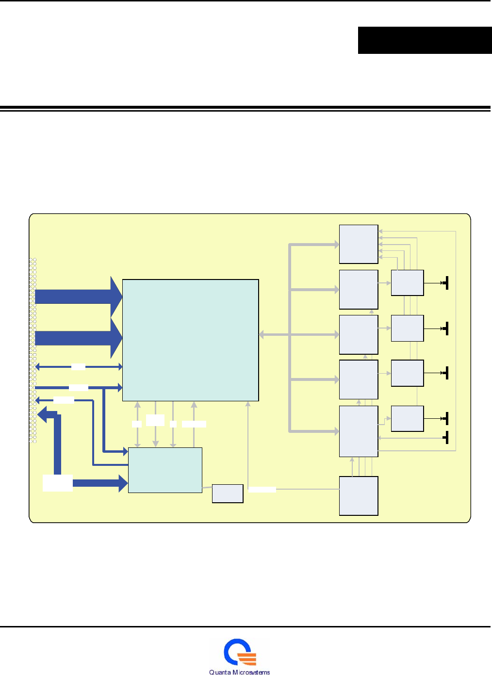
The HM500 WHDI Video Source Unit (VSU) is designed to modulate and transmit downstream video and
audio content over the wireless medium and receive a control channel over the wireless upstream. The
modulation uses 18MHz bandwidth and is carried over the 5GHz unlicensed band. Figure 1 displays a
block diagram of the HM500. The inputs to the VSU are digital uncompressed video, digital audio and control,
all via the WHDI connector. I`t has a MIMO design of four wireless output channels and a slow rate data
input wireless channel. The MiniMAC uC is responsible for the control and the management.
Analog
MUX
(RSSI/
PADET)
VIDEO
MAX2828
PA
5Ghz Tx
Audio
GPIO
RESET
AMN2110
WHDI
TM
Baseband Transmitter
MAX2828
PA
5Ghz Tx
MAX2828
PA
5Ghz Tx
Interrupt
Clock
SPI
20MHz
Int
uC Reset
PA
MAX2828
5Ghz Tx&
Uplink
Control
Two-Wire
uC
MiniMAC
EEPROM
Clock
40M
40M
CLOCK
GEN.
Figure 1: HM500 Block Diagram
Version 1.0
3
Overview
The main building blocks of the HM500 are as follows:
•
AMN2110 WHDI Baseband Transmitter, as briefly described on page 4
•
STM32F103RBT6 Mini-MAC µController, as briefly described on page 4
•
MAX2828 5GHz (802.11a) Transceiver, as briefly described on page 5
•
Power Amplifier (PA), as briefly described on page 5
•
Board Connector (WHDI Connector), as described on page 5
•
EEPROM, as described on page 5
•
40MHz Clock Gen, as described on page 5
2.1
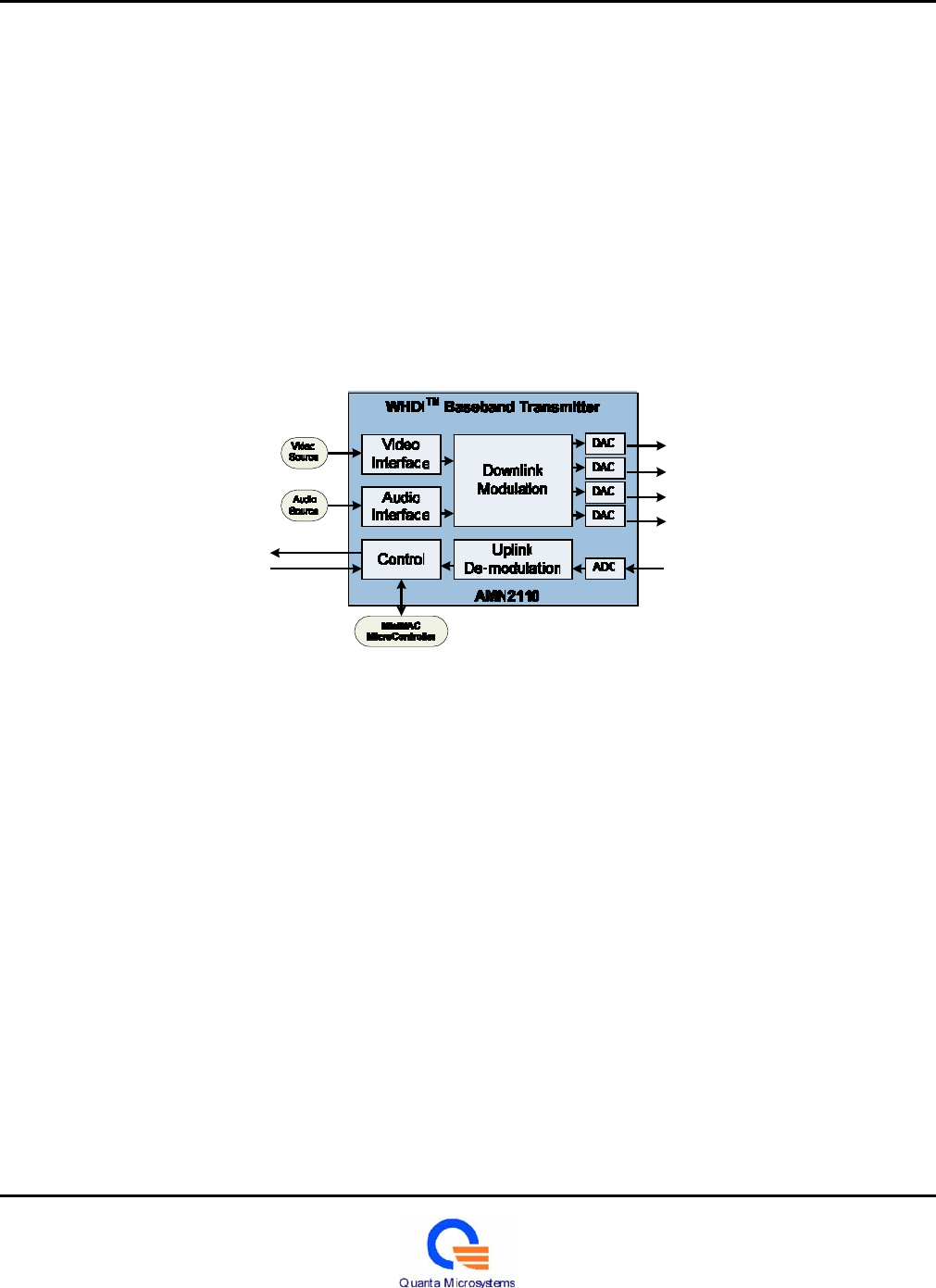
AMN2110 WHDI Baseband Transmitter
The AMN2110 WHDI
TM
baseband transmitter chip is the heart of the HM500 WHDI transmitter module. The
AMN2110 interfaces the A/V source through the WHDI connector, and is controlled on board by the MiniMAC uC.
Figure 2: WHDI Baseband Transmitter Chipset
The AMN2110 is based on MIMO technology transmitting through up to four output
channels. Four digital-to-analog converters and one analog-to-digital converter are embedded within the chip.
The AMN2110 internal PLL accepts an input clock frequency of 40MHz. The input frequency is multiplied and
then used as an internal system clock.
2.2
STM32F103RBT6 Mini-MAC µController
The STM32F103RBT6 microcontroller is based on a 32-bit ARM7TDMI-S CPU, with embedded 128kB high-
speed memory. It is used as an external microcontroller for implementing the MAC layer of the WHDI link.
The STM32F103RBT6 internal PLL accepts an input clock frequency of 40MHz.
Version 1.0
4

Overview
2.3
MAX2828 5GHz (802.11a) Transceiver
The VSU has four MAX2828 chips embedded in it. The MAX2828 is a single-chip, RF transceiver IC designed
specifically for single-band 4.9GHz to 5.875GHz, OFDM, 802.11 WLAN applications. It includes all the circuitry
necessary to implement the RF transceiver function, providing a fully integrated receive path, transmit path, VCO,
frequency synthesizer and baseband/control interface. Only the PA, RF switches, RF bandpass filters (BPF), RF
BALUNs and a small number of passive components are required to form the complete RF front-end solution.
AMIMON's WHDI
TM
technology uses the low cost and high availability of the 802.11a/n RF to allow low-cost RF
for the video modem. Future generations of the WHDI modem will use an AMIMON-designed, cost-efficient,
single-chip, integrated RFIC for multiple transmits on the transmitter side and a single-chip, integrated RFIC for
multiple receivers on the receiver side.
2.4
Power Amplifier (PA)
In order to extend the operating range for the HM500, the RF transmitter uses power amplifiers. Each power
amplifier has an output power detector for TPC purposes. Amimon has implemented Anadigics AWL6951 PA on
the HM500.
2.5
Board Connector (WHDI
TM
Connector)
For information regarding the connector specification and pin-outs, see following section.
2.6
EEPROM
The EEPROM is currently a system option, enabling mating and authentication in a multipoint design
environment.
2.7
40MHz Clock Gen
An on-board 40MHz TCXO is connected to the MAX2828 chipsets and the AMN2110 baseband. The clock is
then divided by two by the AMN2110 and supplied to the STM32F103RBT6 uC.
Version 1.0
5

WHDI Connector Pin-Outs
Chapter 3
WHDI Connector Pin-Outs
3.1
Signals
Table 1: WHDI Connector Signals
# of
Pins Pin Name Description/Functionality Group Direction
Tx Remarks
30 D[29:0] 30-bit RGB (10:10:10) or YCrCb (10:10:10) Video In
1 DCLK Video data clock Video In Up to 78.125
MHz
1 DE Data enable Video In
1 H_SYNC Horizontal sync Video In
1 V_SYNC Vertical sync Video In
1 SPDIF SPDIF audio interface Audio In
1 SCLK I2S continuous serial clock Audio In Up to 3.072Mbps
1 LRCLK I2S Word Select (Left/right clock) which defines also the sampling rate Audio In
1 SDA Two-wire Serial Bus Data (Slave Mode) Control I/O Control I/F for
WHDI
1 SCL Two-wire Serial Bus Clock (Slave Mode) Control In Control I/F for
WHDI
1 INT Interrupt from WHDI module Control Out
1 RESET Reset / Power-down line Control In
1 TBD5 TBD5 is reserved in HM500, HM501 as an option for external power rail
to the on board uC TBD TBD
3 3.3V VCC Power Power
3 3.3V_OR_5V
High Power rail pins,In HM500, HM501 connect these power rail pins to
the 3.3V power rail.
Power Power connect to 3.3V
46 GND Ground Power Power
1 I2S_D0
1 U_GPIO0
1 U_GPIO1
1 USART2_TX
2 N.C.
reserved
Version 1.0
6

WHDI Connector Pin-Outs
3.2
Pin
List
Table 2: Tx WHDI Connector Pin List
Pin Number
Signal
Pin Number Signal
Pin Number Signal
Pin Number Signal
1 RESET 31 D23 61 GND 91
SCLK
2 INT 32 D28 62
GND 92 D1
3 GND 33 GND 63 D7 93 GND
4
GND 34 GND 64
D11 94 GND
5
SCL 35 D21 65
GND 95 LRCLK
6
SDA 36 D26 66
GND 96 D2
7
U_GPIO0 37 GND 67
DCLK 97 GND
8
U_GPIO1 38 GND 68
D9 98 GND
9
USART2_TX 39 D19 69
GND 99 I2S_D0
10
TBD5 40 D25 70
GND 100 D0
11
3.3V_OR_5V 41 GND 71
V_SYNC
12
GND 42 GND 72
D8
13
3.3V_OR_5V 43 D15 73
GND
14
GND 44 D22 74
GND
15
3.3V_OR_5V 45 GND 75
DE
16
GND 46 GND 76
D6
17
3.3V 47 D17 77
GND
18
GND 48 D20 78
GND
19
3.3V 49 GND 79
H_SYNC
20
GND 50 GND 80
D5
21
3.3V 51 D14 81 GND
22
GND 52 D18 82 GND
23
N.C 53 GND 83 SPDIF
24
D29 54 GND 84 D4
25
GND 55 D12 85 GND
26
GND 56
D16 86 GND
27
D24 57
GND 87 N.C
28
D27 58
GND 88 D3
29
GND 59
D10 89 GND
30
GND 60
D13 90 GND
Version 1.0
7
Mechanical Dimensions
Chapter 4
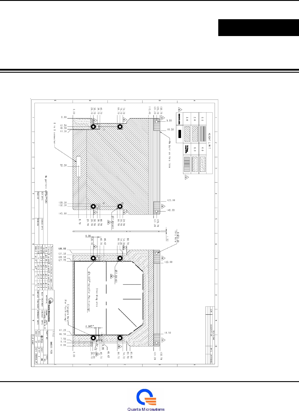
Mechanical Dimensions
The following shows the mechanical dimensions for the HM500:
Figure 3: Mechanical Dimensions
Version 1.0 8

2006/8/16 v1.0
U.S. Regulatory Wireless Notice
Federal Communication Commission Interference Statement
This equipment has been tested and found to comply with the limits for a Class B
digital device, pursuant to Part 15 of the FCC Rules. These limits are designed to
provide reasonable protection against harmful interference in a residential installation.
This equipment generates, uses and can radiate radio frequency energy and, if not
installed and used in accordance with the instructions, may cause harmful
interference to radio communications. However, there is no guarantee that
interference will not occur in a particular installation. If this equipment does cause
harmful interference to radio or television reception, which can be determined by
turning the equipment off and on, the user is encouraged to try to correct the
interference by one of the following measures:
- Reorient or relocate the receiving antenna.
- Increase the separation between the equipment and receiver.
- Connect the equipment into an outlet on a circuit different from that
to which the receiver is connected.
- Consult the dealer or an experienced radio/TV technician for help.
FCC Caution: Any changes or modifications not expressly approved by the party
responsible for compliance could void the user's authority to operate this equipment.
IMPORTANT NOTE:
FCC Radiation Exposure Statement:
This equipment complies with FCC radiation exposure limits set forth for an
uncontrolled environment. This equipment should be installed and operated with
minimum distance 20cm between the radiator & your body.
This transmitter must not be co-located or operating in conjunction with any other
antenna or transmitter.
Operations in the 5.15-5.25GHz band are restricted to indoor usage only.

2006/8/16 v1.0
This device is intended only for OEM integrators under the following
conditions:
1) The antenna must be installed such that 20 cm is maintained between the
antenna and users, and
2) The transmitter module may not be co-located with any other transmitter or
antenna,
As long as 2 conditions above are met, further transmitter test will not be required.
However, the OEM integrator is still responsible for testing their end-product for any
additional compliance requirements required with this module installed (for example,
digital device emissions, PC peripheral requirements, etc.).
IMPORTANT NOTE: In the event that these conditions can not be met (for example
certain laptop configurations or co-location with another transmitter), then the FCC
authorization is no longer considered valid and the FCC ID can not be used on the
final product. In these circumstances, the OEM integrator will be responsible for
re-evaluating the end product (including the transmitter) and obtaining a separate
FCC authorization.
End Product Labeling
This transmitter module is authorized only for use in device where the antenna may
be installed such that 20 cm may be maintained between the antenna and users. The
final end product must be labeled in a visible area with the following: “Contains FCC
ID:. T5U-HM500
Manual Information To the End User
The OEM integrator has to be aware not to provide information to the end user
regarding how to install or remove this RF module in the user’s manual of the end
product which integrates this module.
The end user manual shall include all required regulatory information/warning as show
in this manual.

2006/8/16 v1.0
Canadian Regulatory Wireless Notice
This device complies with RSS-210 of the Industry Canada Rules. Operation is subject
to the following two conditions:
1) this device may not cause interference and
2) this device must accept any interference, including interference that may cause
undesired operation of the device
Caution:
The device for the band 5150-5250 MHz is only for indoor usage to reduce potential for
harmful interference to co-channel mobile satellite systems.
IMPORTANT NOTE:
IC Radiation Exposure Statement:
This equipment complies with IC radiation exposure limits set forth for an uncontrolled
environment. This equipment should be installed and operated with minimum distance
20cm between the radiator and your body.