Quectel Wireless Solutions 201202M10 GSM/GPRS Module User Manual M10 HD V3 0x
Quectel Wireless Solutions Company Limited GSM/GPRS Module M10 HD V3 0x
UserManual.wiki
>
Quectel Wireless Solutions
>
201202M10 User Manual
Users Manual
Navigation menu
Upload a User Manual
Namespaces
Wiki Guide
HTML
PDF
Info
Views
User Manual
Discussion / Help
Navigation

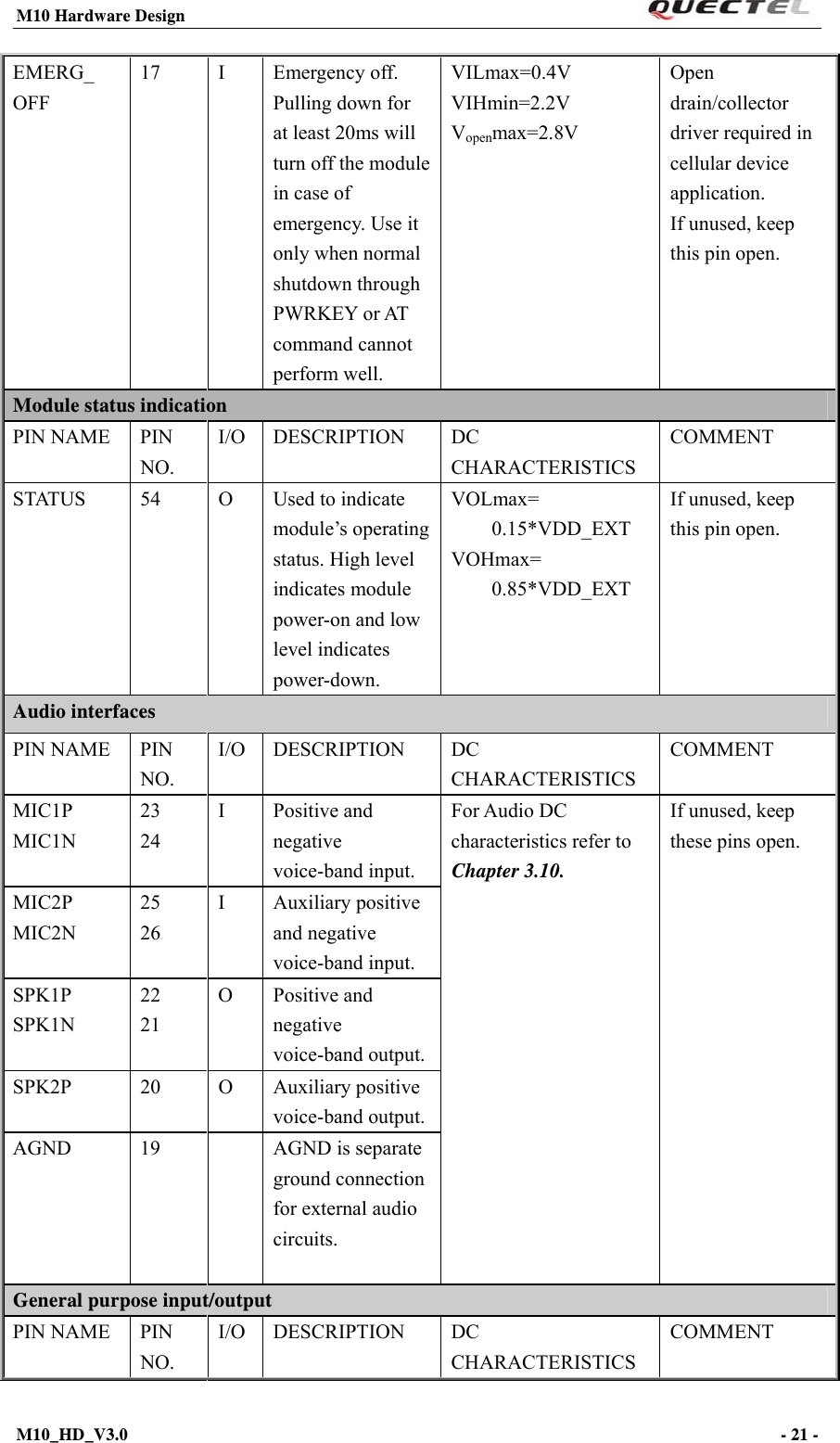
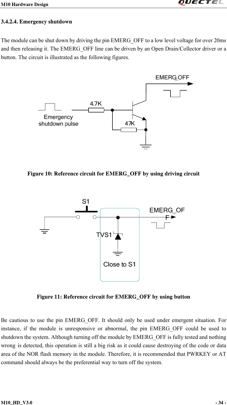
![M10 Hardware Design M10_HD_V3.0 - 9 - 1. Introduction This document defines the M10 module and describes the hardware interface of M10 module which are connected with the customer application and the air interface. This document can help customer quickly understand module interface specifications, electrical and mechanical details. Associated with application notes and user guide, customer can use M10 module to design and set up mobile applications easily. 1.1. Related documents Table 1: Related documents SN Document name Remark [ 1] M10_ATC AT comm a n d s s e t [2] ITU-T Draft new recommendation V.25ter Serial asynchronous automatic dialing and control [3] GSM 07.07 Digital cellular telecommunications (Phase 2+); AT command set for GSM Mobile Equipment (ME) [4] GSM 07.10 Support GSM 07.10 multiplexing protocol [5] GSM 07.05 Digital cellular telecommunications (Phase 2+); Use of Data Terminal Equipment – Data Circuit terminating Equipment (DTE – DCE) interface for Short Message Service (SMS) and Cell Broadcast Service (CBS) [6] GSM 11.14 Digital cellular telecommunications (Phase 2+); Specification of the SIM Application Toolkit for the Subscriber Identity module – Mobile Equipment (SIM – ME) interface [7] GSM 11.11 Digital cellular telecommunications (Phase 2+); Specification of the Subscriber Identity module – Mobile Equipment (SIM – ME) interface [8] GSM 03.38 Digital cellular telecommunications (Phase 2+); Alphabets and language-specific information [9] GSM 11.10 Digital cellular telecommunications (Phase 2); Mobile Station (MS) conformance specification; Part 1: Conformance specification [10] GSM_UART_AN UART port application notes [11] M10_HD_AN01 M10 hardware design application notes [12] GSM_FW_Upgrade_AN01 GSM Firmware upgrade application note [13] M10_EVB_UGD M10 EVB user guide application notes](https://usermanual.wiki/Quectel-Wireless-Solutions/201202M10/User-Guide-1659940-Page-10.png)

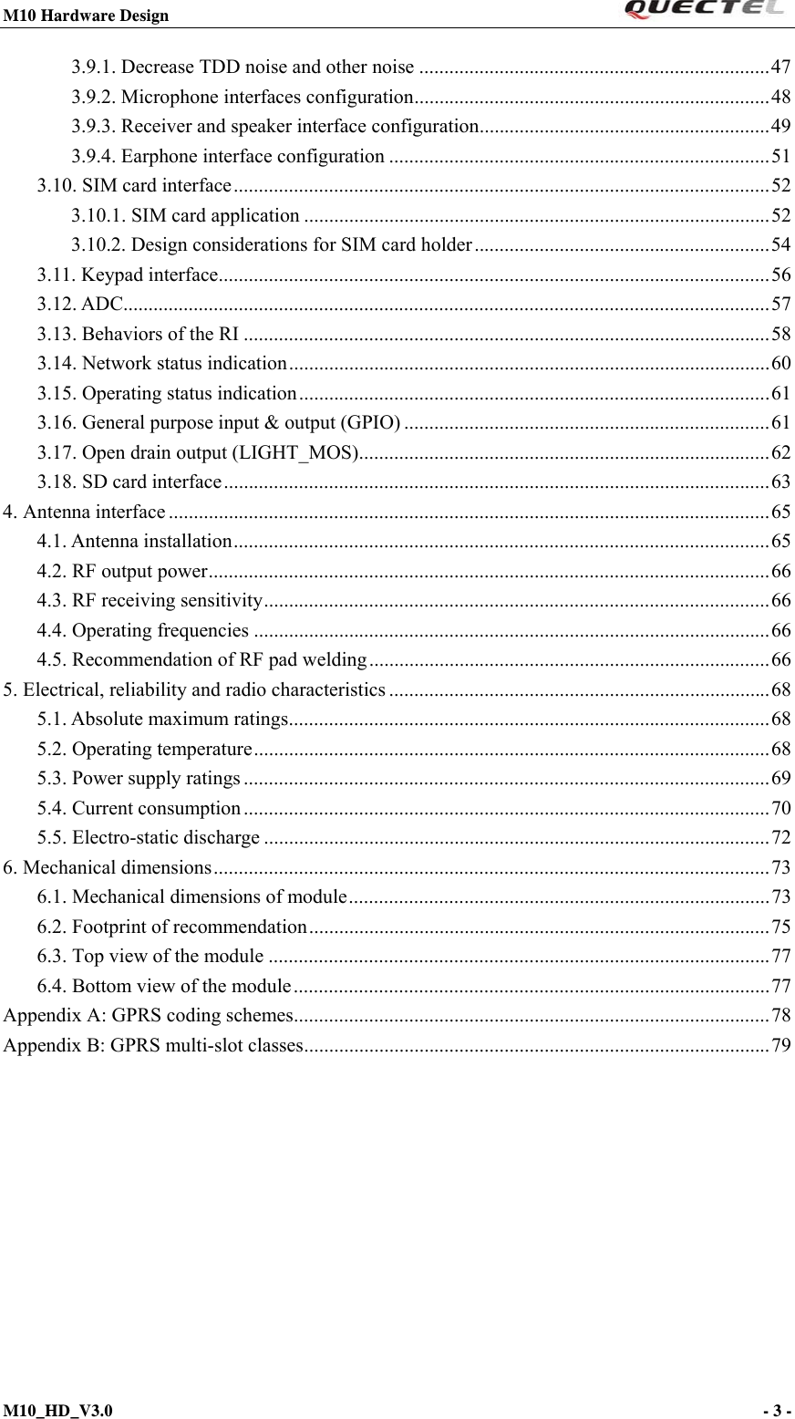
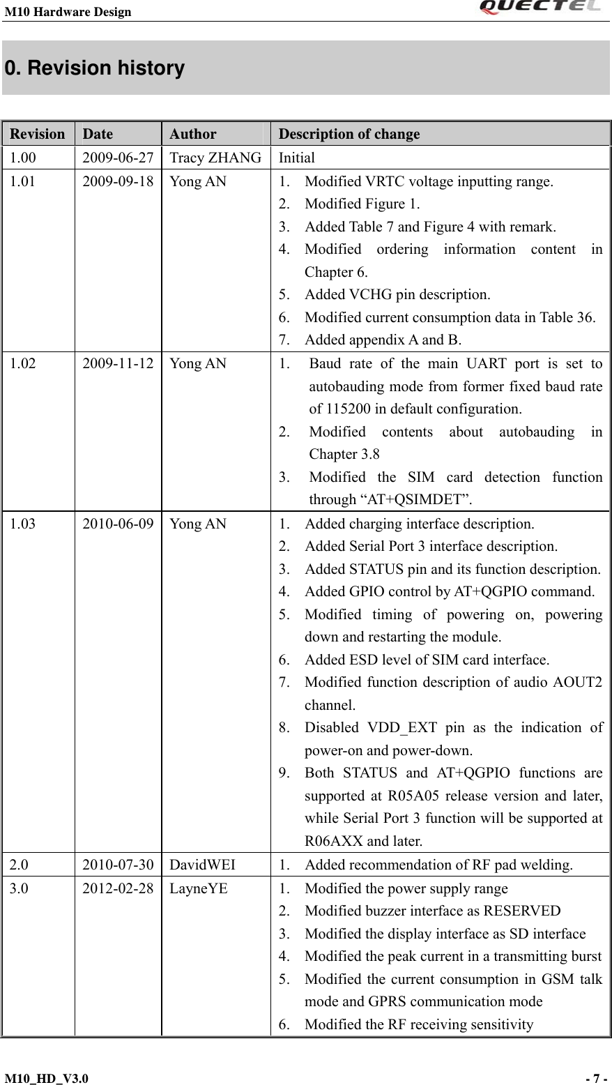
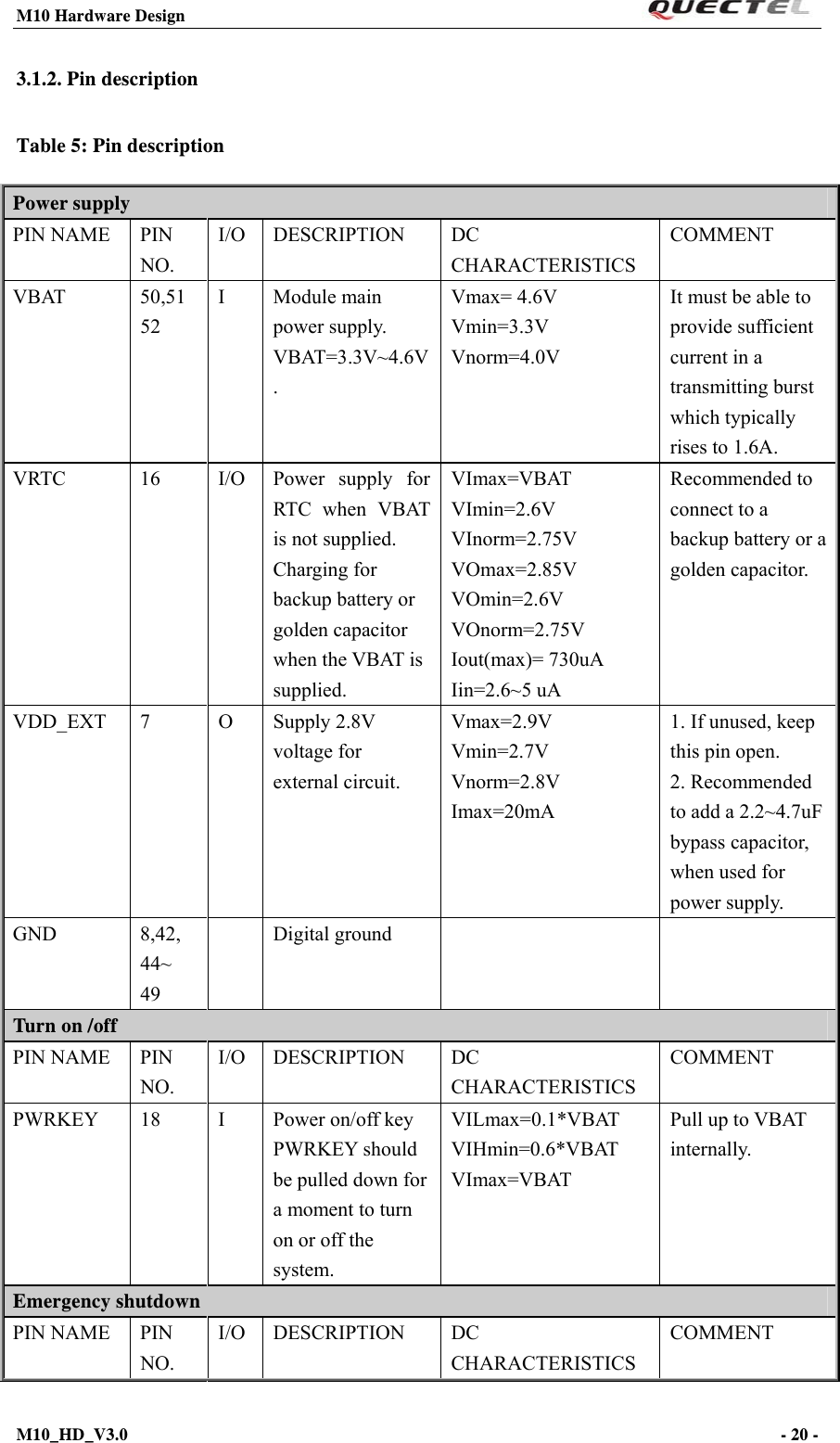
![M10 Hardware Design M10_HD_V3.0 - 18 - Figure 1: Module functional diagram2.3. Evaluation board In order to help customer on the application of M12, Quectel supplies an Evaluation Board (EVB) that hosts the module directly with appropriate power supply, SIM card holder, RS-232 serial interface, handset RJ11 port, earphone port, antenna and other peripherals to control or test the module. For details, please refer to the document [13].](https://usermanual.wiki/Quectel-Wireless-Solutions/201202M10/User-Guide-1659940-Page-19.png)
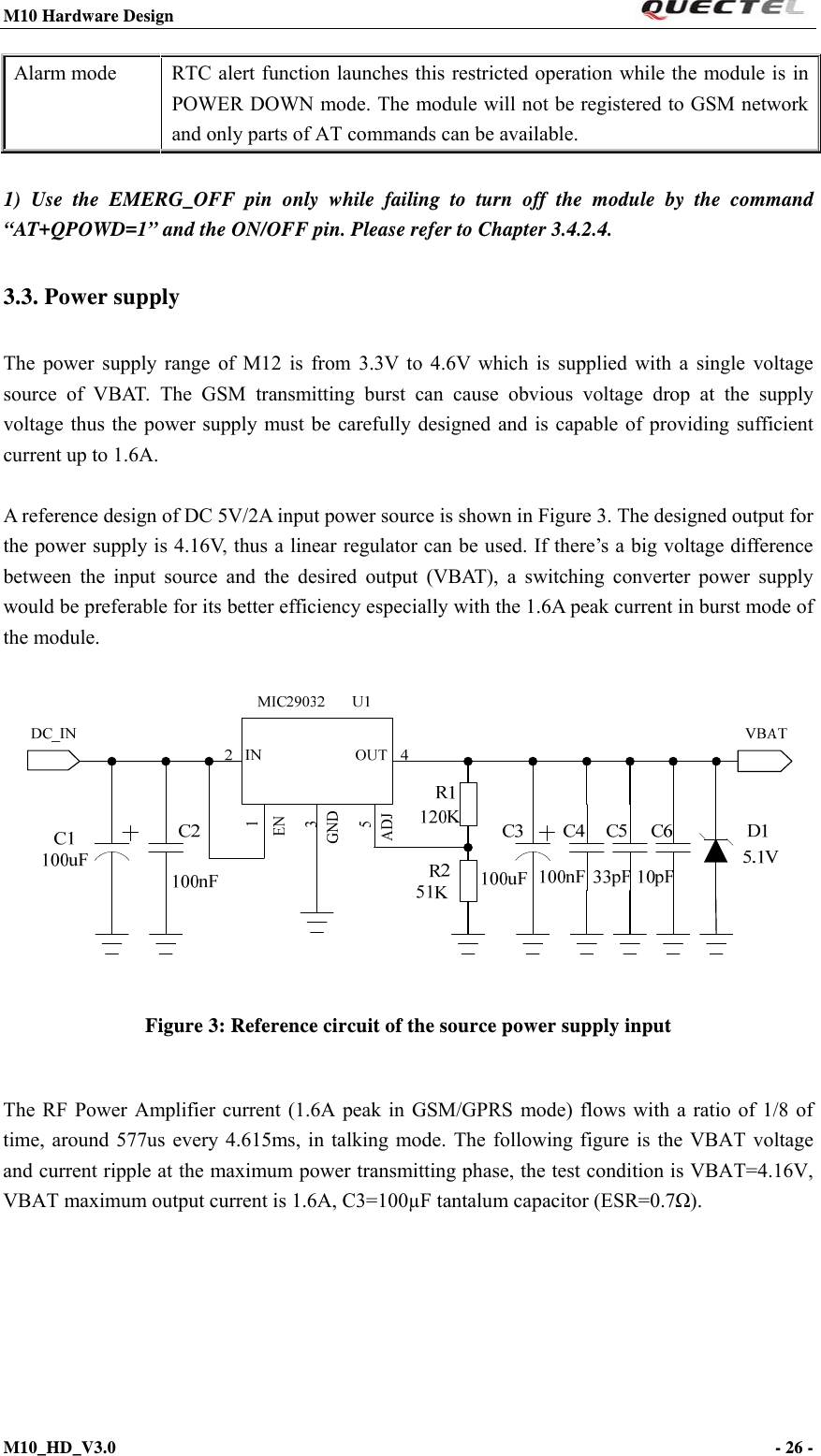
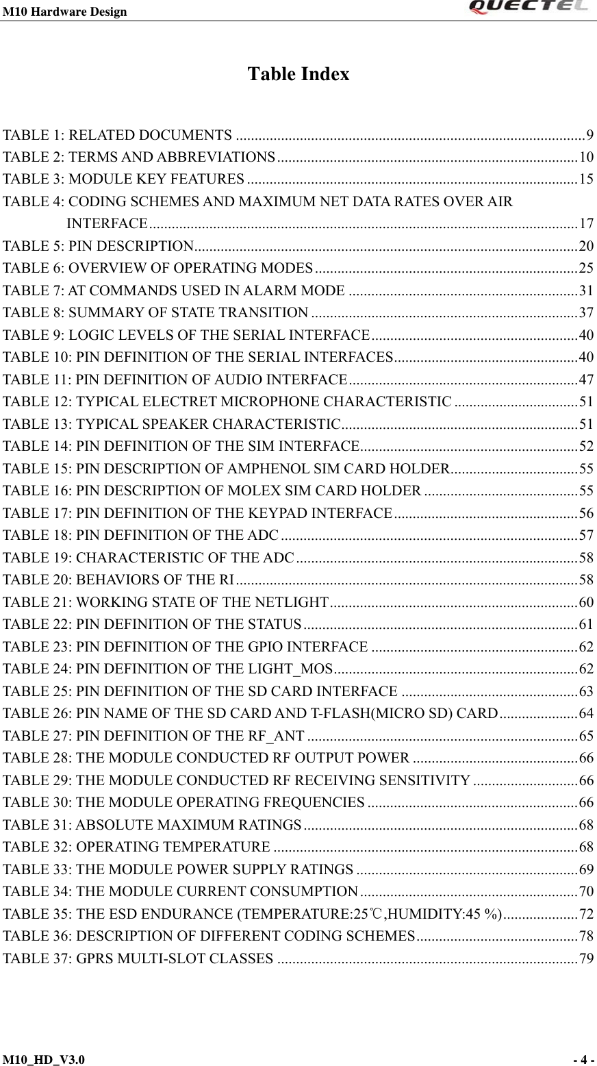
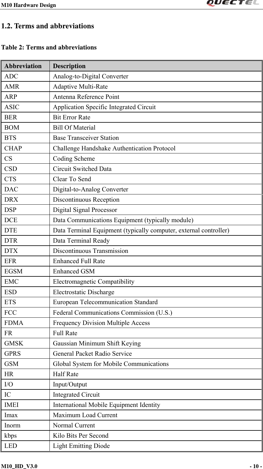
![M10 Hardware Design M10_HD_V3.0 - 28 - C1>=100uF; C2=0.1uF~1uF; C3=10pF; C4=33pF Figure 5: Reference circuit of the VBAT input3.3.3. Monitor power supply To monitor the supply voltage, you can use the “AT+CBC” command which includes three parameters: charging status, remaining battery capacity and voltage value (in mV). It returns the 0-100 percent of battery capacity and actual value measured between VBAT and GND. The voltage is continuously measured at an interval depending on the operating mode. The displayed voltage (in mV) is averaged over the last measuring period before the “AT+CBC” command is executed. For details, please refer to document [1]. 3.4. Power up and down scenarios 3.4.1. Power on The module can be turned on through the two ways, which are described in following chapters: Via PWRKEY pin: start normal operating mode (please refer to chapter 3.4.1.1); Via RTC interrupt: start ALARM mode (please refer to chapter 3.4.1.2). Note: The module is set to autobauding mode (AT+IPR=0) in default configuration. In the autobauding mode, the URC “RDY” is not sent to host controller after powering on. AT command can be sent to the module 2-3 seconds after the module is powered on. Host controller should firstly send an “AT” or “at” string in order that the module can detect baud rate of host controller, and it should send the second or the third “AT” or “at” string until receiving “OK” string from module. Then an “AT+IPR=x;&W” should be sent to set a fixed baud rate for](https://usermanual.wiki/Quectel-Wireless-Solutions/201202M10/User-Guide-1659940-Page-29.png)
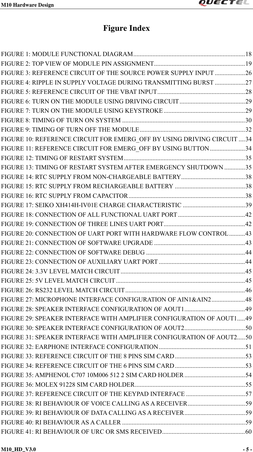
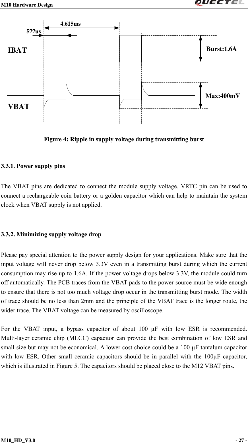
![M10 Hardware Design M10_HD_V3.0 - 29 - module and save the configuration to flash memory of module. After these configurations, the URC “RDY” would be received from the Serial Port of module every time when the module is powered on. Refer to Chapter “AT+IPR” in document [1]. 3.4.1.1. Power on module using the PWRKEY pin Customer’s application can turn on the module by driving the pin PWRKEY to a low level voltage and after STATUS pin outputs a high level, PWRKEY pin can be released. Customer may monitor the level of the STATUS pin to judge whether the module is power-on or not. An open collector driver circuit is suggested to control the PWRKEY. A simple reference circuit is illustrated in Figure 6. Figure 6: Turn on the module using driving circuit The other way to control the PWRKEY is using a button directly. A TVS component is indispensable to be placed nearby the button for ESD protection. When pressing the key, electrostatic strike may generate from finger. A reference circuit is showed in Figure 7. Figure 7: Turn on the module using keystroke](https://usermanual.wiki/Quectel-Wireless-Solutions/201202M10/User-Guide-1659940-Page-30.png)
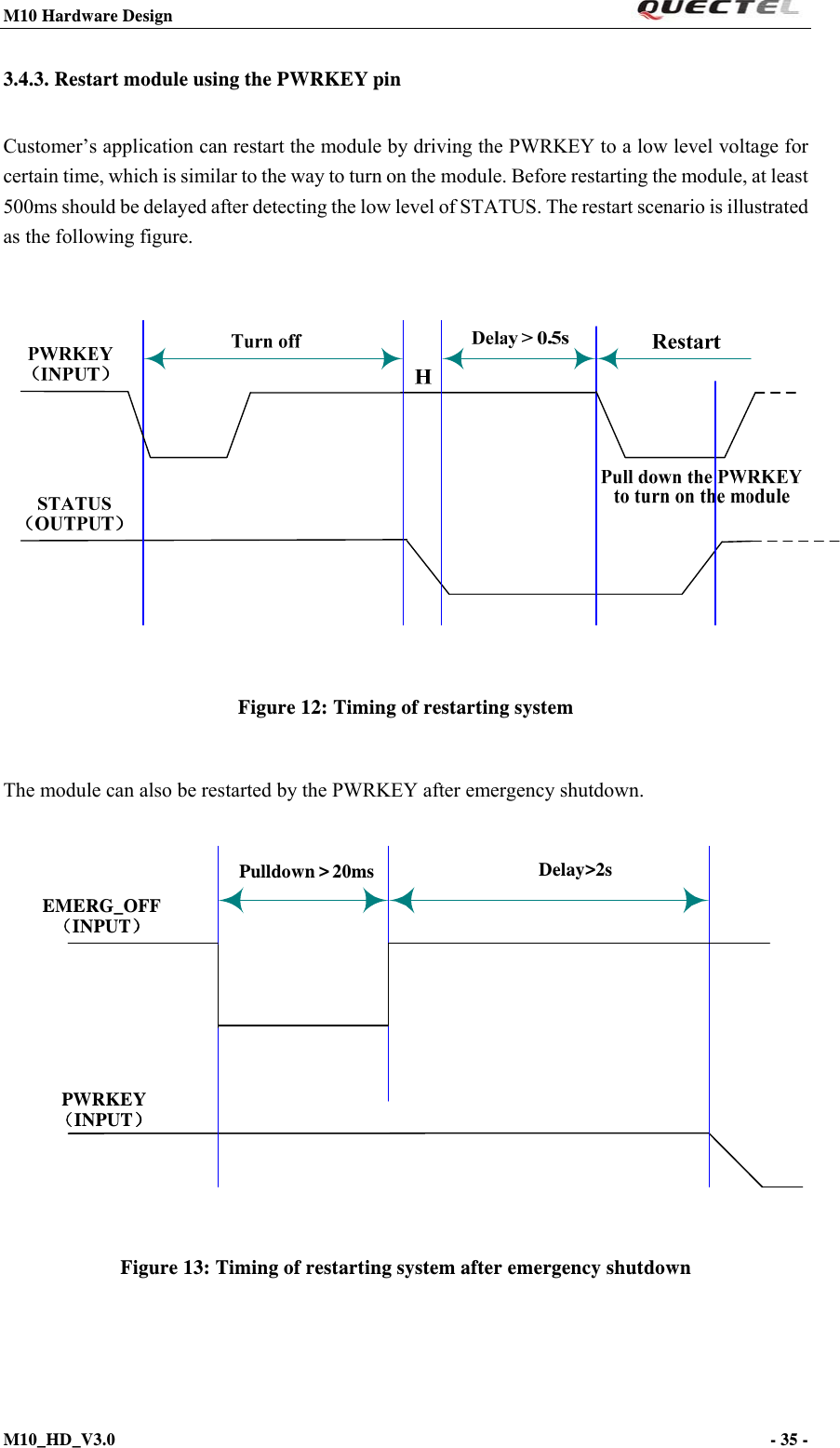
![M10 Hardware Design M10_HD_V3.0 - 31 - the module will go into the alarm mode. In this case, the module will send out an Unsolicited Result Code (URC) when the baud rate of the Serial Port is set to a fixed one. RDY ALARM MODE +CFUN:0 Note: This result code does not appear when autobauding is active because a valid baud rate is not available immediately after powering up the module. Therefore, the module is recommended to set to a fixed baud rate. During alarm mode, use “AT+CFUN” command to query the status of software protocol stack; it will return “0” which indicates that the protocol stack is closed. After 90 seconds, the module will power down automatically. However, if the GSM protocol stack is started by “AT+CFUN=1” command during the alarm mode, the process of automatic power-off will not be executed. In alarm mode, driving the PWRKEY to a low level voltage for a period will cause the module to power down. The frequently-used AT commands during alarm mode are briefly summarized In Table 7. For details of these instructions, please refer to document [1]. Table 7: AT commands used in alarm mode AT command Function AT+QALARM Set alarm time AT+CCLK Set data and time of RTC AT+QPOWD Power down the module AT+CFUN Start or close the protocol stack 3.4.2. Power down The following procedures can be used to turn off the module: Normal power down procedure: Turn off module using the PWRKEY pin Normal power down procedure: Turn off module using command “AT+QPOWD” Over-voltage or under-voltage automatic shutdown: Take effect when over-voltage or under-voltage is detected Emergent power down procedure: Turn off module using the EMERG_OFF pin](https://usermanual.wiki/Quectel-Wireless-Solutions/201202M10/User-Guide-1659940-Page-32.png)
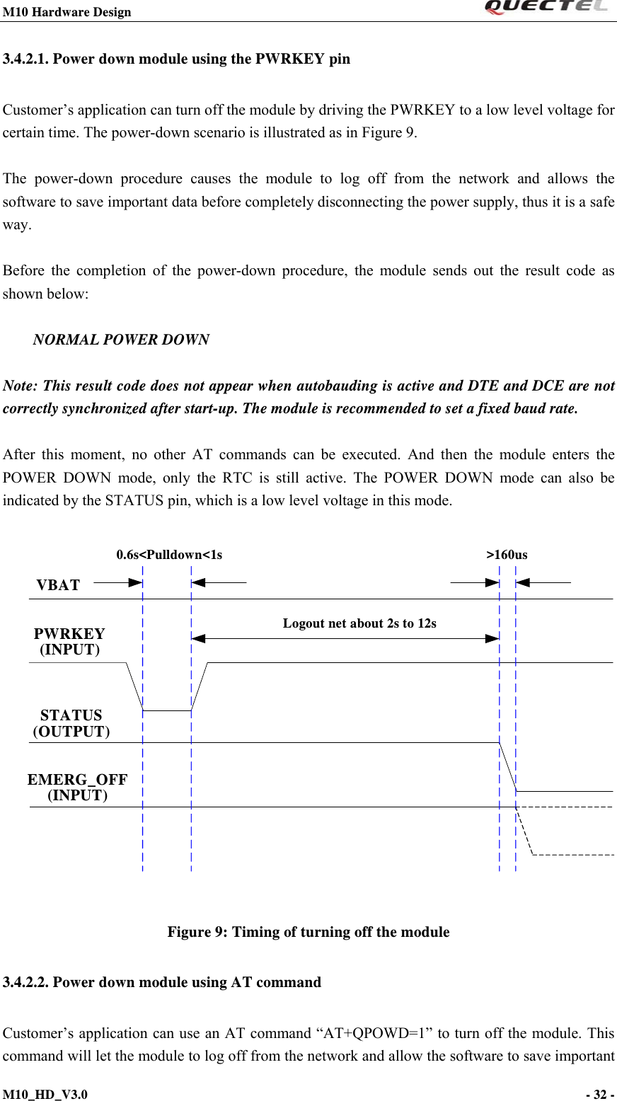
![M10 Hardware Design M10_HD_V3.0 - 33 - data before completely disconnecting the power supply, thus it is a safe way. Before the completion of the power-down procedure, the module sends out the result code as shown below: NORMAL POWER DOWN After this moment, no other AT commands can be executed. And then the module enters the POWER DOWN mode, only the RTC is still active. The POWER DOWN mode can also be indicated by STATUS pin, which is a low level voltage in this mode. For details about the AT command of “AT+QPOWD”, please refer to document [1]. 3.4.2.3. Over-voltage or under-voltage automatic shutdown The module will constantly monitor the voltage applied on the VBAT, if the voltage is ≤ 3.5V, the following URC will be presented: UNDER_VOLTAGE WARNING If the voltage is ≥ 4.5V, the following URC will be presented: OVER_VOLTAGE WARNING The normal input voltage range is 3.3V to 4.6V. If the voltage is > 4.6V or <3.3V, the module would automatically shutdown itself. If the voltage is <3.3V, the following URC will be presented: UNDER_VOLTAGE POWER DOWN If the voltage is >4.6V, the following URC will be presented: OVER_VOLTAGE POWER DOWN Note: These result codes don’t appear when autobauding is active and DTE and DCE are not correctly synchronized after start-up. The module is recommended to set to a fixed baud rate. After this moment, no other AT command can be executed, the module logs off from network and enters POWER DOWN mode, and only RTC is still active. The POWER DOWN mode can also be indicated by the pin STATUS, which is a low level voltage in this mode.](https://usermanual.wiki/Quectel-Wireless-Solutions/201202M10/User-Guide-1659940-Page-34.png)
![M10 Hardware Design M10_HD_V3.0 - 36 - 3.5. Power saving Upon system requirement, there are several actions to drive the module to enter low current consumption status. For example, “AT+CFUN” can be used to set the module into minimum functionality mode and DTR hardware interface signal can be used to lead system to SLEEP mode. 3.5.1. Minimum functionality mode Minimum functionality mode reduces the functionality of the module to minimum level, thus minimizes the current consumption when the slow clocking mode is activated at the same time. This mode is set with the “AT+CFUN” command which provides the choice of the functionality levels <fun>=0,1,4. 0: minimum functionality 1: full functionality (default) 4: disable both transmitting and receiving of RF part If the module is set to minimum functionality by “AT+CFUN=0”, the RF function and SIM card function would be closed. In this case, the serial port is still accessible, but all AT commands correlative with RF function or SIM card function will not be accessible. If the module has been set by “AT+CFUN=4”, the RF function will be closed but the serial port is still active. In this case, all AT commands correlative with RF function will not be accessible. After the module is set by “AT+CFUN=0” or “AT+CFUN=4”, it can return to full functionality by “AT+CFUN=1”. For detailed information about “AT+CFUN”, please refer to document [1]. 3.5.2. SLEEP mode (slow clock mode) The SLEEP mode is disabled in default software configuration. Customer’s application can enable this mode by “AT+QSCLK=1”. On the other hand, the default setting is “AT+QSCLK=0” and in this mode, the module cannot enter SLEEP mode. When “AT+QSCLK=1” is set to the module, customer’s application can control the module to enter or exit from the SLEEP mode through pin DTR. When DTR is set to high level, and there is no on-air or hardware interrupt such as GPIO interrupt or data on serial port, the module will enter SLEEP mode automatically. In this mode, the module can still receive voice, SMS or GPRS paging from network but the serial port is not accessible.](https://usermanual.wiki/Quectel-Wireless-Solutions/201202M10/User-Guide-1659940-Page-37.png)
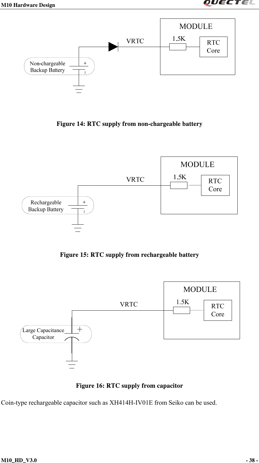
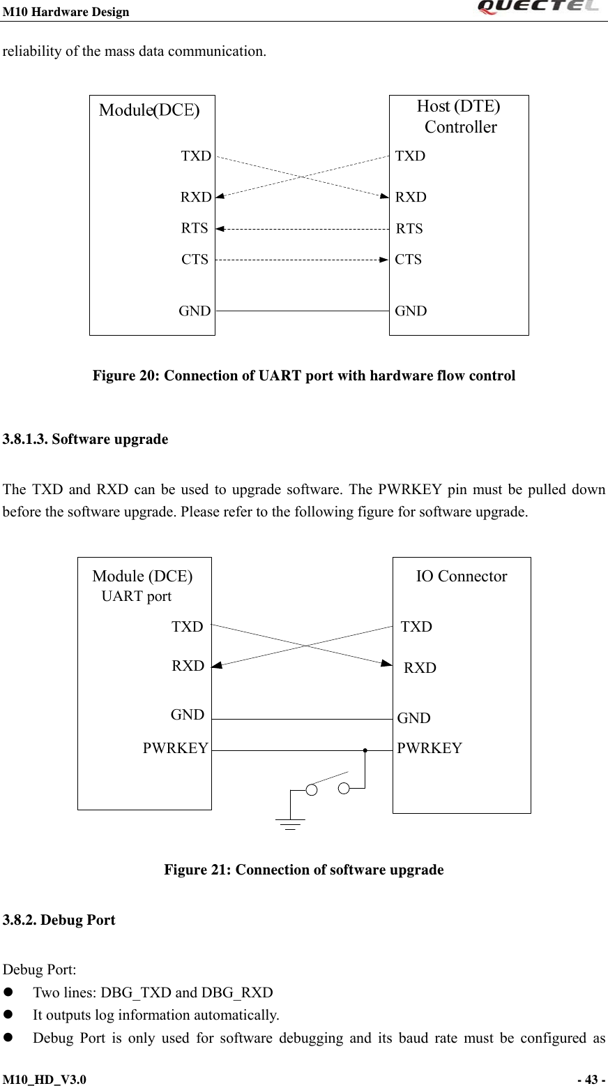
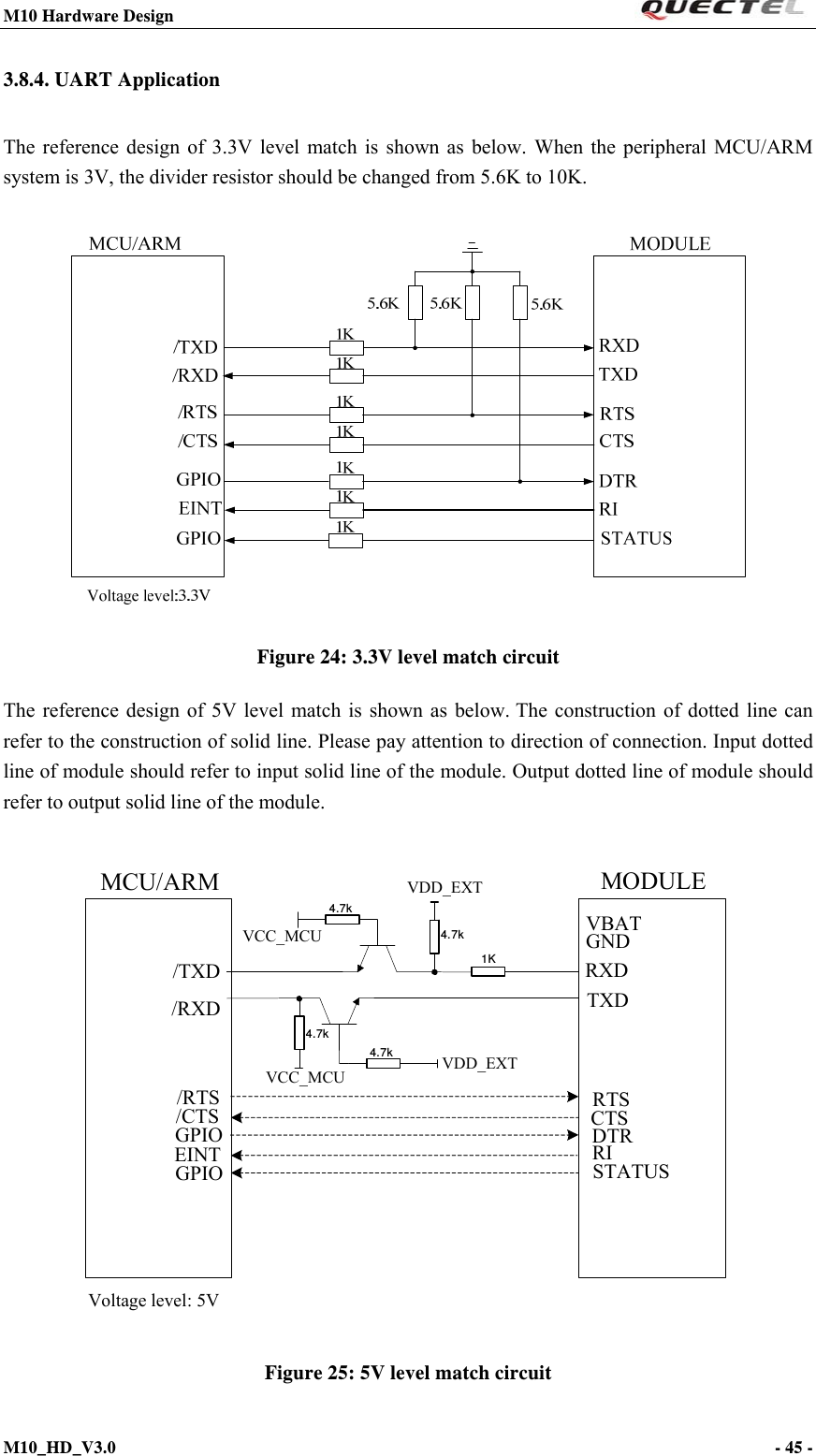
![M10 Hardware Design M10_HD_V3.0 - 39 - Figure 17: Seiko XH414H-IV01E Charge Characteristic 3.8. Serial interfaces The module provides two unbalanced asynchronous serial ports including Serial Port, Debug Port. The module is designed as a DCE (Data Communication Equipment), following the traditional DCE-DTE (Data Terminal Equipment) connection. Autobauding function supports baud rate from 4800bps to 115200bps. The UART Port: TXD: Send data to RXD of DTE RXD: Receive data from TXD of DTE RTS: Requests to send CTS: Clear to send DTR: DTE is ready and inform DCE (this pin can wake the module up) RI: Ring indicator (when the call, SMS, data of the module are coming, the module will output signal to inform DTE) DCD: Data carrier detection (the validity of this pin demonstrates the communication link is set up) Note: The module disables hardware flow control by default. When hardware flow control is required, RTS and CTS should be connected to the host. AT command “AT+IFC=2,2” is used to enable hardware flow control. AT command “AT+IFC=0,0” is used to disable the hardware flow control. For more details, please refer to document [1].](https://usermanual.wiki/Quectel-Wireless-Solutions/201202M10/User-Guide-1659940-Page-40.png)
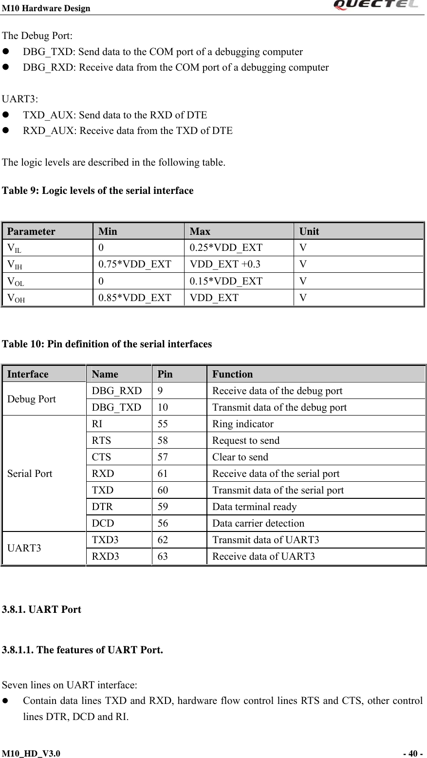
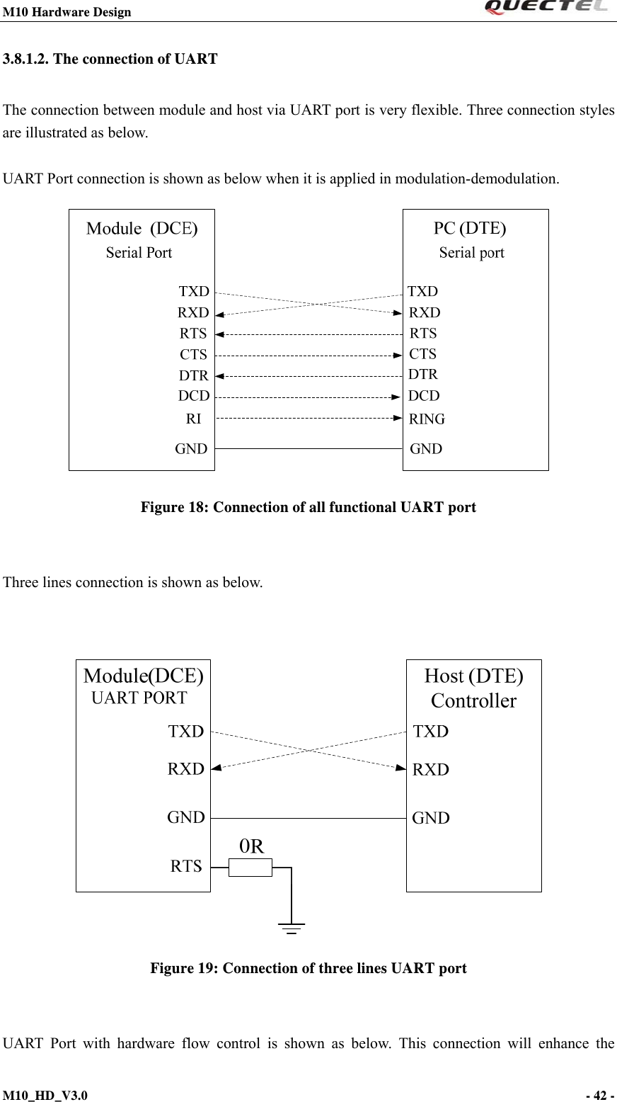
![M10 Hardware Design M10_HD_V3.0 - 41 - The module disables hardware flow control in default, AT command “AT+IFC=2,2” is used to enable hardware flow control. Used for AT command, GPRS data, CSD FAX, etc. Multiplexing function is supported on the UART Port. So far only the basic mode of multiplexing is available. Support the communication baud rates as the following: 300,600,1200,2400,4800,9600,14400,19200,28800,38400,57600,115200. The default setting is autobauding mode. Support the following baud rates for Autobauding function: 4800, 9600, 19200, 38400, 57600, 115200. After setting a fixed baud rate or Autobauding, please send “AT” or “at” string at that rate. The UART port is ready when it responds with “OK”. Autobauding allows the module to detect the baud rate by receiving the string “AT” or “at” from the host or PC automatically, which gives module flexibility without considering which baud rate is used by the host controller. Autobauding is enabled by default. To take advantage of the autobauding mode, special attention should be paid according to the following requirements: Synchronization between DTE and DCE: When DCE (the module) powers on with the autobauding enabled, it is recommended to wait 2 to 3 seconds before sending the first “AT” string. After receiving the “OK” response, DTE and DCE are correctly synchronized. If the host controller needs URC in the mode of autobauding, it must be synchronized first. Otherwise the URC will be discarded. Restrictions on autobauding operation The UART port has to be operated at 8 data bits, no parity and 1 stop bit (factory setting). The A/ and a/ commands can’t be used. Only the strings “AT” or “at” can be detected (neither “At” nor “aT”). The Unsolicited Result Codes like “RDY”, “+CFUN: 1” and “+CPIN: READY” will not be indicated when the module is turned on with autobauding enabled and not be synchronized. Any other Unsolicited Result Codes will be sent at the previous baud rate before the module detects the new baud rate by receiving the first “AT” or “at” string. The DTE may receive unknown characters after switching to new baud rate. It is not recommended to switch to autobauding from a fixed baud rate. If autobauding is active it is not recommended to switch to multiplex mode Note: To assure reliable communication and avoid any problems caused by undetermined baud rate between DCE and DTE, it is strongly recommended to configure a fixed baud rate and save it instead of using autobauding after start-up. For more details, please refer to Section “AT+IPR” in document [1].](https://usermanual.wiki/Quectel-Wireless-Solutions/201202M10/User-Guide-1659940-Page-42.png)
![M10 Hardware Design M10_HD_V3.0 - 44 - 460800bps. Figure 22: Connection of software debug3.8.3. UART Port 3 UART3: Two data lines: TXD3and RXD3 UART3 port is used for AT command only and does not support GPRS data, CSD FAX, Multiplexing function etc. Support the communication baud rates as the following: 4800, 9600, 14400, 19200,28800,38400,57600,115200. The default baud rate setting is 115200bps, and does not support autobauding. The baud rate can be modified by AT+QSEDCB command. For more details, please refer to document [1]. Figure 23: Connection of Auxiliary UART port](https://usermanual.wiki/Quectel-Wireless-Solutions/201202M10/User-Guide-1659940-Page-45.png)
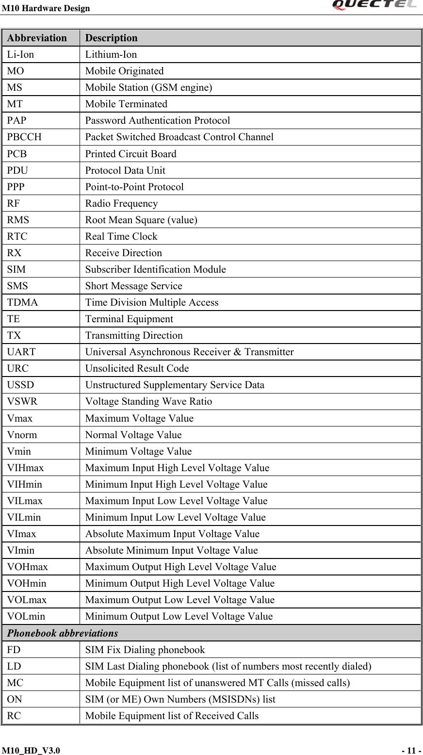
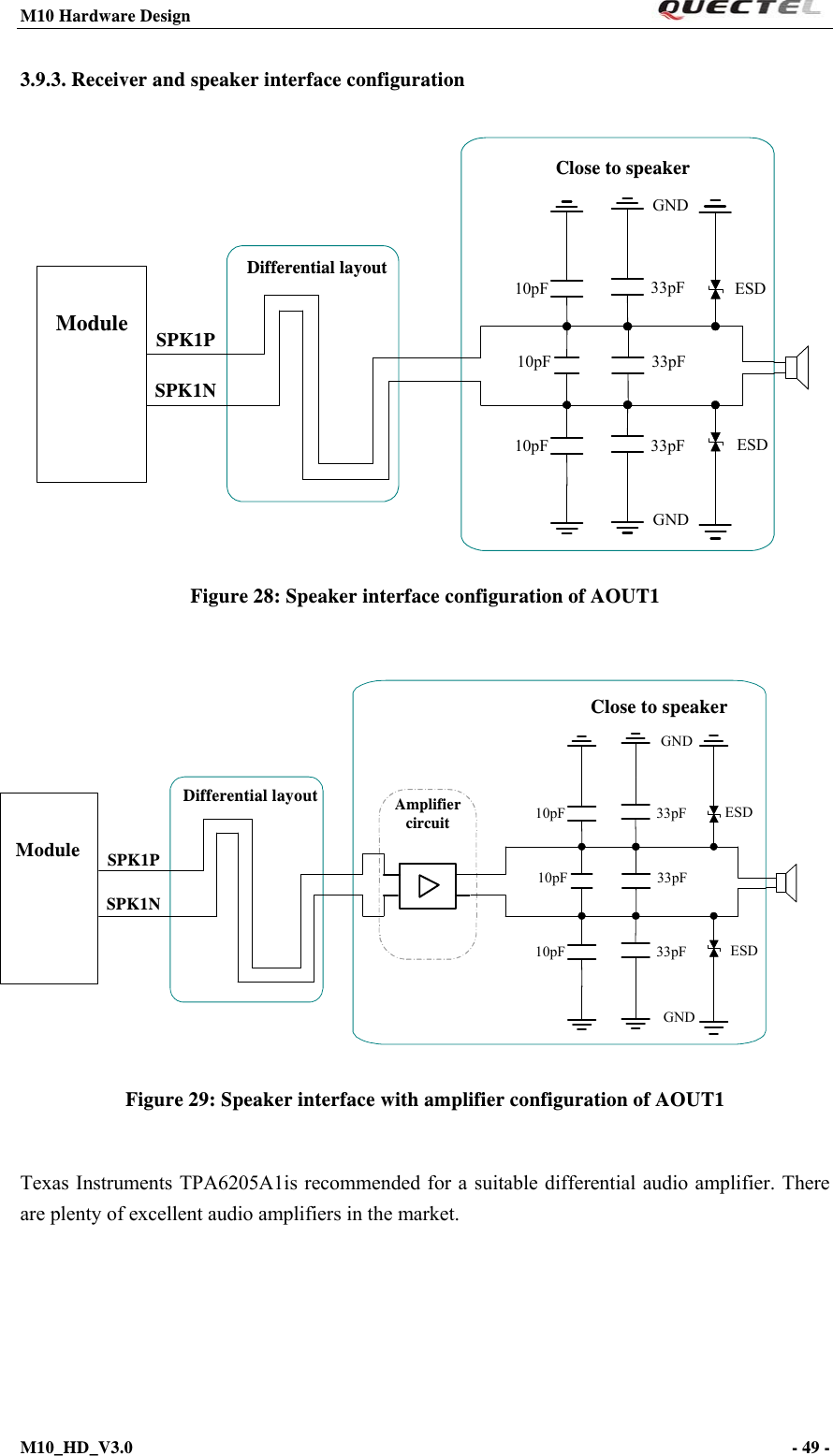
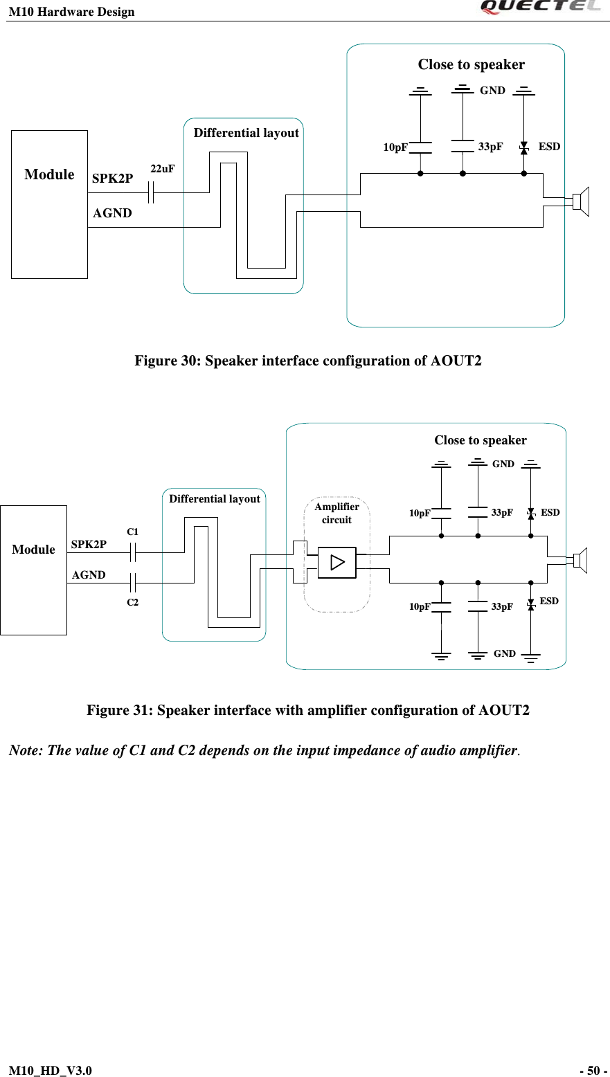
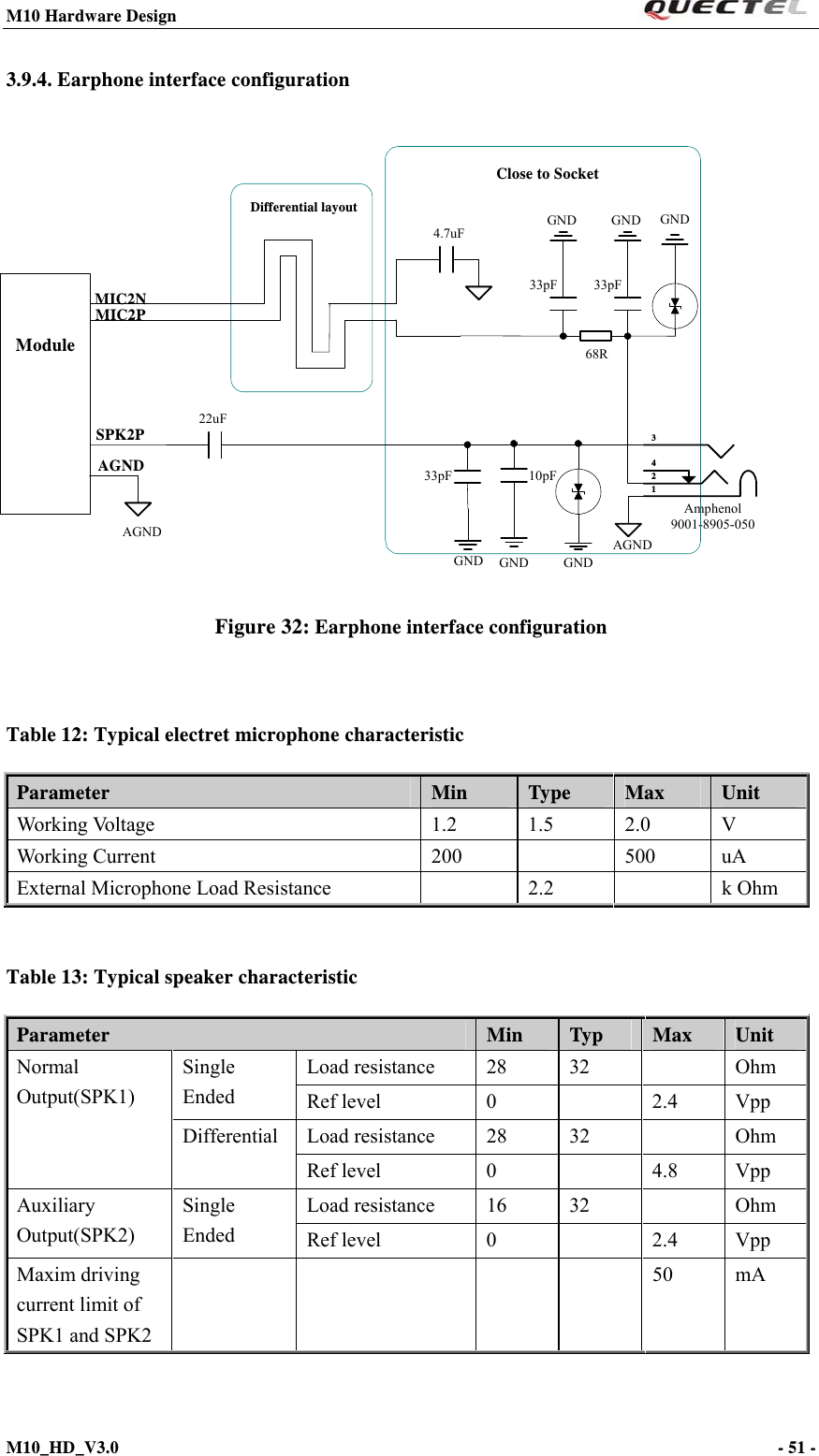
![M10 Hardware Design M10_HD_V3.0 - 47 - Table 11: Pin definition of Audio interface AIN1 and AIN2, which may be used for both microphone and line inputs. An electret microphone is usually used. AIN1 and AIN2 are both differential input channels. AOUT1 and AOUT2, which may be used for both receiver and speaker outputs. AOUT1 channel is typically used for a receiver built into a handset, while AOUT2 channel is typically used with headset or hands-free speaker. AOUT1 channel is a differential channel and AOUT2 is a single-ended channel. SPK2P and AGND can establish a pseudo differential mode. If customer needs to play Melody or Midi ringtone for incoming call, AOUT2 Channel should always be used. These two audio channels can be swapped by “AT+QAUDCH” command. For more details, please refer to document [1]. Use AT command “AT+QAUDCH” to select audio channel: 0--AIN1/AOUT1 (normal audio channel), the default value is 0. 1--AIN2/AOUT2 (aux audio channel). For each channel, customer can use AT+QMIC to adjust the input gain level of microphone. Customer can also use “AT+CLVL” to adjust the output gain level of receiver and speaker. “AT+QECHO” is to set the parameters for echo cancellation control. “AT+QSIDET” is to set the side-tone gain level. For more details, please refer to document [1]. 3.9.1. Decrease TDD noise and other noise The 33pF capacitor is applied for filtering out 850MHz/900MHz RF interference when the module is transmitting at GSM900MHz. Without placing this capacitor, TDD noise could be heard. Moreover, the 10pF capacitor here is for filtering out 1800MHz/1900MHz RF interference. However, the resonant frequency point of a capacitor largely depends on the material and production technique. Therefore, customer would have to discuss with its capacitor vendor to choose the most suitable capacitor for filtering out GSM850MHz, GSM900MHz, DCS1800MHz and PCS1900MHz separately. Interface Name Pin Function (AIN1/AOUT1) MIC1P 23 Microphone1 input + MIC1N 24 Microphone1 input - SPK1P 22 Audio1 output+ SPK1N 21 Audio1 output- (AIN2/AOUT2) MIC2P 25 Microphone2 input + MIC2N 26 Microphone2 input - SPK2P 20 Audio2 output+ AGND 19 Suggested to be used in audio circuit. Do not connect to digital GND in host PCB as it could produce TDD noise.](https://usermanual.wiki/Quectel-Wireless-Solutions/201202M10/User-Guide-1659940-Page-48.png)
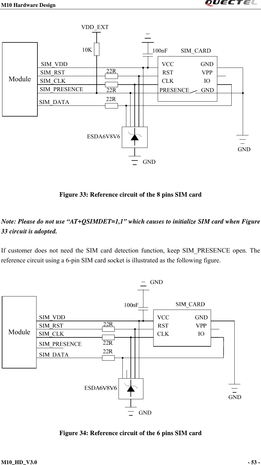
![M10 Hardware Design M10_HD_V3.0 - 52 - 3.10. SIM card interface 3.10.1. SIM card application The SIM interface supports the functionality of the GSM Phase 1 specification and also supports the functionality of the new GSM Phase 2+ specification for FAST 64 kbps SIM card, which is intended for use with a SIM application Tool-kit. The SIM interface is powered from an internal regulator in the module. Both 1.8V and 3.0V SIM Cards are supported. Table 14: Pin definition of the SIM interface Figure 33 is the reference circuit for SIM interface, and here an 8-pin SIM card holder is used. The pin SIM_PRESENCE is used to detect whether the tray of the Molex SIM socket, which is used for holding SIM card, is present in the card socket. When the tray is inserted in the socket, SIM_PRESENCE is at low level. Regardless of the SIM card is in the tray or not, the change of SIM_PRESENCE level from high to low level prompts the module to reinitialize SIM card. In default configuration, SIM card detection function is disabled. Customer’s application can use “AT+QSIMDET=1,0 ” to be switched on and “AT+QSIMDET=0,0 ” to switch off the SIM card detection function. For detail of this AT command, please refer to document [1]. When “AT+QSIMDET=1,0” is set and the tray with SIM card is removed from SIM socket, the following URC will be presented. +CPIN: NOT READY When the tray with SIM card is inserted into SIM socket again and the module finishes re-initializing SIM card, the following URC will be presented. Call Ready Name Pin Function SIM_VDD 12 Supply power for SIM Card. Automatic detection of SIM card voltage. 3.0V±10% and 1.8V±10%. Maximum supply current is around 10mA. SIM_DATA 13 SIM Card data I/O SIM_CLK 14 SIM Card Clock SIM_RST 15 SIM Card Reset SIM_PRESENCE 11 SIM Card Presence](https://usermanual.wiki/Quectel-Wireless-Solutions/201202M10/User-Guide-1659940-Page-53.png)
![M10 Hardware Design M10_HD_V3.0 - 57 - KBR4KBR3KBR2KBR1KBR0KBC0KBC1KBC2KBC3KBC4ModuleGPIO1_KBC5 Figure 37: Reference circuit of the keypad interface If a 5*5 matrix does not provide enough keys, GPIO1 could be multiplexed as KBC5 to configure a 5*6 keypad matrix. Then, the keypad interface consists of 5 keypad row outputs and 6 keypad column inputs. The basic configuration is 5 keypad rows and 6 keypad columns, giving 30 keys. Note: This function is not supported in the default firmware. 3.12. ADC The module provides two auxiliary ADC interfaces to measure the values of two analog inputs. AT command “AT+QADC?” is used to read the voltage value present on ADC0 pin. AT command “AT+QEADC?” is used to read the voltage value present on ADC1 pin. For details of this AT command, please refer to document [1]. Table 18: Pin definition of the ADC Name Pin Function ADC0 41 Analog to digital converter. ADC1 40 Analog to digital converter](https://usermanual.wiki/Quectel-Wireless-Solutions/201202M10/User-Guide-1659940-Page-58.png)
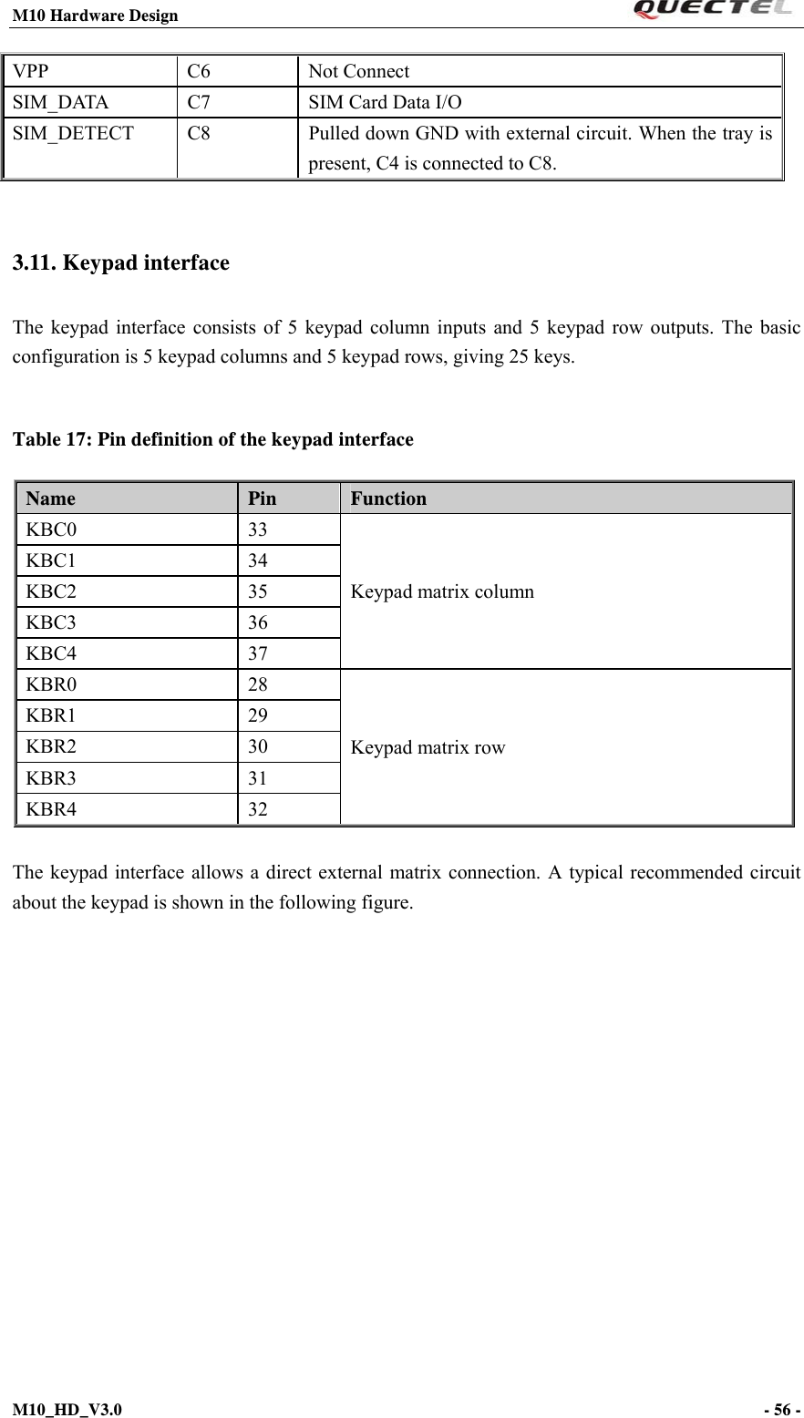
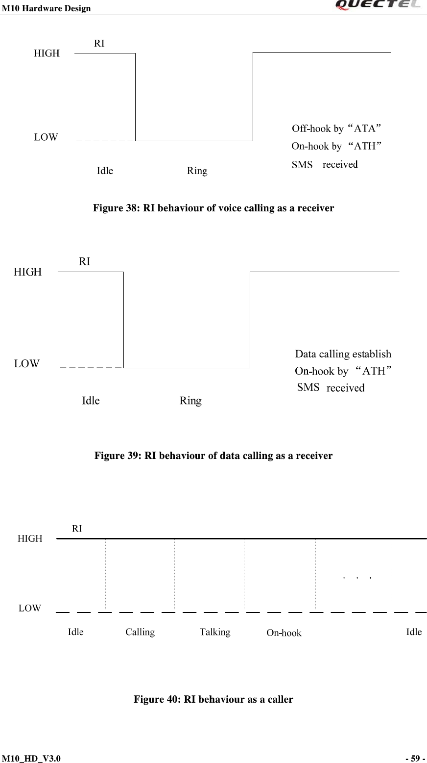
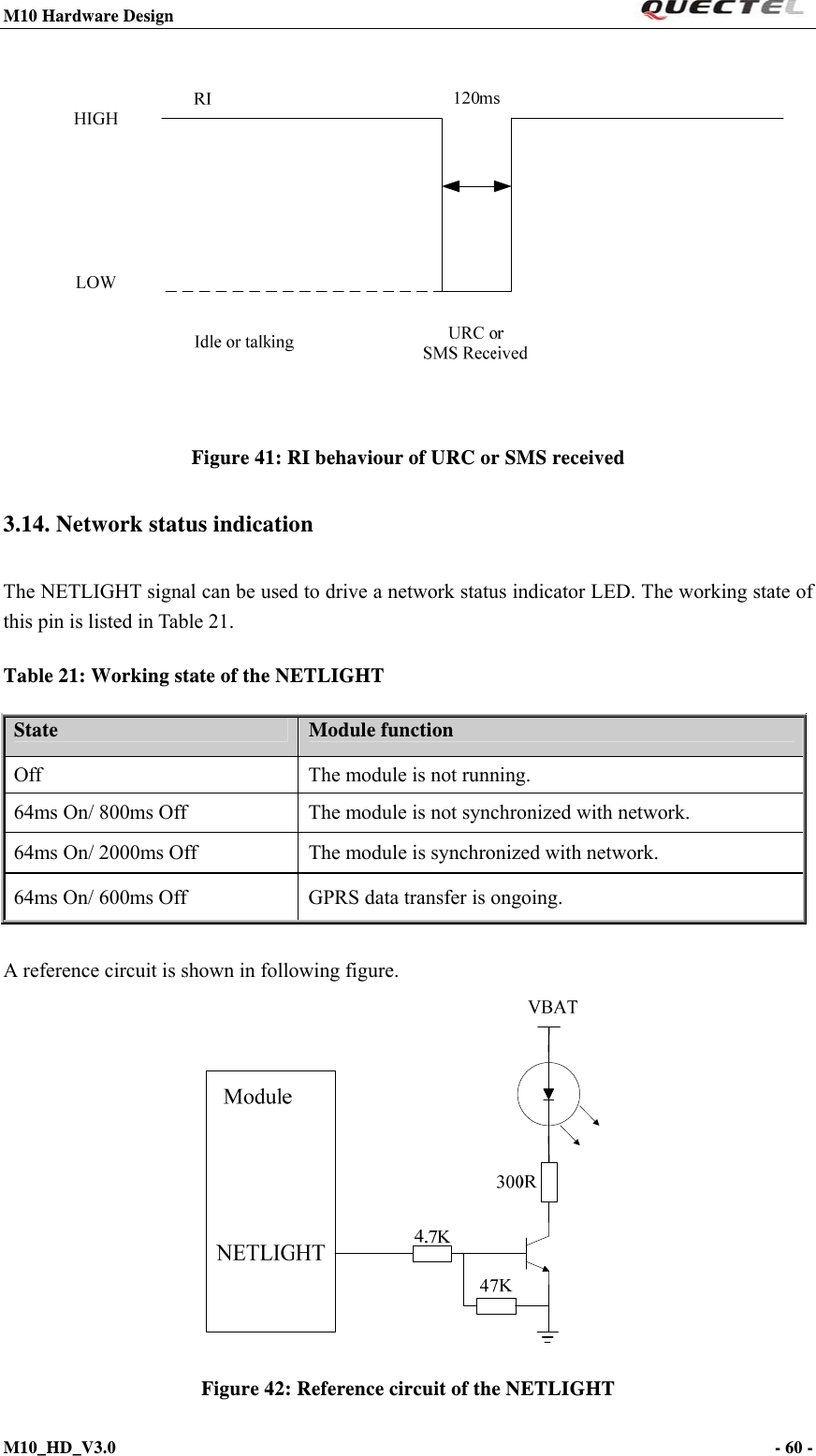
![M10 Hardware Design M10_HD_V3.0 - 58 - Table 19: Characteristic of the ADC Item Min Typ Max Units Voltage range 0 2.8 V ADC Resolution 10 bits ADC accuracy 2.7 mV 3.13. Behaviors of the RI Table 20: Behaviors of the RI State RI response Standby HIGH Voice calling Changed to LOW, then: 1. Changed to HIGH when call is established. 2. Use ATH to hang up the call, RI changes to HIGH. 3. Calling part hangs up, RI changes to HIGH first, and changes to LOW for 120ms indicating “NO CARRIER” as an URC, then changes to HIGH again. 4. Change to HIGH when SMS is received. Data calling Changed to LOW, then: 1. Changed to HIGH when data connection is established. 2. Use ATH to hang up the data calling, RI changes to HIGH. 3. Calling part hangs up, RI changes to HIGH first, and changes to LOW for 120ms indicating “NO CARRIER” as an URC, then changes to HIGH again. 4. Changed to HIGH when SMS is received. SMS When a new SMS comes, the RI changes to LOW and holds low level for about 120 ms, then changes to HIGH. URC Certain URCs can trigger 120ms low level on RI. For more details, please refer to the document [10] If the module is used as a caller, the RI would maintain high except the URC or SMS is received. On the other hand, when it is used as a receiver, the timing of the RI is shown below.](https://usermanual.wiki/Quectel-Wireless-Solutions/201202M10/User-Guide-1659940-Page-59.png)
![M10 Hardware Design M10_HD_V3.0 - 61 - 3.15. Operating status indication The STATUS pin is set as an output pin and can be used to judge whether module is power-on, please refer to Chapter 3.4. In customer design, this pin can be connected to a GPIO of DTE or be used to drive an LED in order to judge the module’s operation status. A reference circuit is shown in figure 43. Table 22: Pin definition of the STATUS Figure 43: Reference circuit of the STATUS 3.16. General purpose input & output (GPIO) The module provides a limited number of General Purpose Input/Output signal pins. The driving capability of these pins is 4mA. Every GPIO can be configured as input or output, and set to high or low when working as an output pin by “AT+CEQGPIO” command. Before using these GPIO pins, customer should configure them with “AT+CEQGPIO=1,x,x,x,x” first. For details, please refer to document [1]. Name Pin Function STATUS 54 Indicate module’s operating status](https://usermanual.wiki/Quectel-Wireless-Solutions/201202M10/User-Guide-1659940-Page-62.png)