Quectel Wireless Solutions 201202M10 GSM/GPRS Module User Manual M10 HD V3 0x
Quectel Wireless Solutions Company Limited GSM/GPRS Module M10 HD V3 0x
Users Manual
M10
Quectel Cellular Engine
Hardware Design
M10_HD_V3.0

M10 Hardware Design
M10_HD_V3.0 - 1 -
Document Title M10 Hardware Design
Revision 3.0
Date 2012-03-02
Status Released
Document Control ID M10_HD_V3.0
General Notes
Quectel offers this information as a service to its customers, to support application and
engineering efforts that use the products designed by Quectel. The information provided is
based upon requirements specifically provided for customers of Quectel. Quectel has not
undertaken any independent search for additional information, relevant to any information
that may be in the customer’s possession. Furthermore, system validation of this product
designed by Quectel within a larger electronic system remains the responsibility of the
customer or the customer’s system integrator. All specifications supplied herein are subject to
change.
Copyright
This document contains proprietary technical information of Quectel Co., Ltd. Copying of
this document, distribution to others, and communication of the contents thereof, are
forbidden without permission. Offenders are liable to the payment of damages. All rights are
reserved in the event of a patent grant or registration of a utility model or design. All
specification supplied herein are subject to change without notice at any time.
Copyright © Quectel Wireless Solutions Co., Ltd. 2012

M10 Hardware Design
M10_HD_V3.0 - 2 -
Contents
Contents ............................................................................................................................................ 2
Table Index ........................................................................................................................................ 4
Figure Index ...................................................................................................................................... 5
0. Revision history ............................................................................................................................ 7
1. Introduction ................................................................................................................................... 9
1.1. Related documents .............................................................................................................. 9
1.2. Terms and abbreviations .................................................................................................... 10
1.3. Directives and standards .................................................................................................... 12
1.3.1. FCC Statement ........................................................................................................ 12
1.3.2. FCC Radiation exposure statement ......................................................................... 12
1.3.3. Industry Canada licence .......................................................................................... 12
1.4. Safety cautions .................................................................................................................. 13
2. Product concept ........................................................................................................................... 15
2.1. Key features ...................................................................................................................... 15
2.2. Functional diagram ............................................................................................................ 17
2.3. Evaluation board ............................................................................................................... 18
3. Application interface ................................................................................................................... 19
3.1. Pin of module .................................................................................................................... 19
3.1.1. Pin assignment ......................................................................................................... 19
3.1.2. Pin description ......................................................................................................... 20
3.2. Operating modes ............................................................................................................... 25
3.3. Power supply ..................................................................................................................... 26
3.3.1. Power supply pins.................................................................................................... 27
3.3.2. Minimizing supply voltage drop.............................................................................. 27
3.3.3. Monitor power supply ............................................................................................. 28
3.4. Power up and down scenarios ........................................................................................... 28
3.4.1. Power on .................................................................................................................. 28
3.4.2. Power down ............................................................................................................. 31
3.4.3. Restart module using the PWRKEY pin.................................................................. 35
3.5. Power saving ..................................................................................................................... 36
3.5.1. Minimum functionality mode .................................................................................. 36
3.5.2. SLEEP mode (slow clock mode) ............................................................................. 36
3.5.3. Wake up module from SLEEP mode ...................................................................... 37
3.6. Summary of state transitions (except SLEEP mode) ......................................................... 37
3.7. RTC backup ...................................................................................................................... 37
3.8. Serial interfaces ................................................................................................................. 39
3.8.1. UART Port .............................................................................................................. 40
3.8.2. Debug Port ............................................................................................................... 43
3.8.3. UART Port 3 ........................................................................................................... 44
3.8.4. UART Application .................................................................................................. 45
3.9. Audio interfaces................................................................................................................. 46

M10 Hardware Design
M10_HD_V3.0 - 3 -
3.9.1. Decrease TDD noise and other noise ...................................................................... 47
3.9.2. Microphone interfaces configuration ....................................................................... 48
3.9.3. Receiver and speaker interface configuration .......................................................... 49
3.9.4. Earphone interface configuration ............................................................................ 51
3.10. SIM card interface ........................................................................................................... 52
3.10.1. SIM card application ............................................................................................. 52
3.10.2. Design considerations for SIM card holder ........................................................... 54
3.11. Keypad interface .............................................................................................................. 56
3.12. ADC................................................................................................................................. 57
3.13. Behaviors of the RI ......................................................................................................... 58
3.14. Network status indication ................................................................................................ 60
3.15. Operating status indication .............................................................................................. 61
3.16. General purpose input & output (GPIO) ......................................................................... 61
3.17. Open drain output (LIGHT_MOS) .................................................................................. 62
3.18. SD card interface ............................................................................................................. 63
4. Antenna interface ........................................................................................................................ 65
4.1. Antenna installation ........................................................................................................... 65
4.2. RF output power ................................................................................................................ 66
4.3. RF receiving sensitivity ..................................................................................................... 66
4.4. Operating frequencies ....................................................................................................... 66
4.5. Recommendation of RF pad welding ................................................................................ 66
5. Electrical, reliability and radio characteristics ............................................................................ 68
5.1. Absolute maximum ratings ................................................................................................ 68
5.2. Operating temperature ....................................................................................................... 68
5.3. Power supply ratings ......................................................................................................... 69
5.4. Current consumption ......................................................................................................... 70
5.5. Electro-static discharge ..................................................................................................... 72
6. Mechanical dimensions ............................................................................................................... 73
6.1. Mechanical dimensions of module .................................................................................... 73
6.2. Footprint of recommendation ............................................................................................ 75
6.3. Top view of the module .................................................................................................... 77
6.4. Bottom view of the module ............................................................................................... 77
Appendix A: GPRS coding schemes ............................................................................................... 78
Appendix B: GPRS multi-slot classes ............................................................................................. 79

M10 Hardware Design
M10_HD_V3.0 - 4 -
Table Index
TABLE 1: RELATED DOCUMENTS ............................................................................................. 9
TABLE 2: TERMS AND ABBREVIATIONS ................................................................................ 10
TABLE 3: MODULE KEY FEATURES ........................................................................................ 15
TABLE 4: CODING SCHEMES AND MAXIMUM NET DATA RATES OVER AIR
INTERFACE .................................................................................................................. 17
TABLE 5: PIN DESCRIPTION ...................................................................................................... 20
TABLE 6: OVERVIEW OF OPERATING MODES ...................................................................... 25
TABLE 7: AT COMMANDS USED IN ALARM MODE ............................................................. 31
TABLE 8: SUMMARY OF STATE TRANSITION ....................................................................... 37
TABLE 9: LOGIC LEVELS OF THE SERIAL INTERFACE ....................................................... 40
TABLE 10: PIN DEFINITION OF THE SERIAL INTERFACES ................................................. 40
TABLE 11: PIN DEFINITION OF AUDIO INTERFACE ............................................................. 47
TABLE 12: TYPICAL ELECTRET MICROPHONE CHARACTERISTIC ................................. 51
TABLE 13: TYPICAL SPEAKER CHARACTERISTIC ............................................................... 51
TABLE 14: PIN DEFINITION OF THE SIM INTERFACE .......................................................... 52
TABLE 15: PIN DESCRIPTION OF AMPHENOL SIM CARD HOLDER .................................. 55
TABLE 16: PIN DESCRIPTION OF MOLEX SIM CARD HOLDER ......................................... 55
TABLE 17: PIN DEFINITION OF THE KEYPAD INTERFACE ................................................. 56
TABLE 18: PIN DEFINITION OF THE ADC ............................................................................... 57
TABLE 19: CHARACTERISTIC OF THE ADC ........................................................................... 58
TABLE 20: BEHAVIORS OF THE RI ........................................................................................... 58
TABLE 21: WORKING STATE OF THE NETLIGHT .................................................................. 60
TABLE 22: PIN DEFINITION OF THE STATUS ......................................................................... 61
TABLE 23: PIN DEFINITION OF THE GPIO INTERFACE ....................................................... 62
TABLE 24: PIN DEFINITION OF THE LIGHT_MOS ................................................................. 62
TABLE 25: PIN DEFINITION OF THE SD CARD INTERFACE ............................................... 63
TABLE 26: PIN NAME OF THE SD CARD AND T-FLASH(MICRO SD) CARD ..................... 64
TABLE 27: PIN DEFINITION OF THE RF_ANT ........................................................................ 65
TABLE 28: THE MODULE CONDUCTED RF OUTPUT POWER ............................................ 66
TABLE 29: THE MODULE CONDUCTED RF RECEIVING SENSITIVITY ............................ 66
TABLE 30: THE MODULE OPERATING FREQUENCIES ........................................................ 66
TABLE 31: ABSOLUTE MAXIMUM RATINGS ......................................................................... 68
TABLE 32: OPERATING TEMPERATURE ................................................................................. 68
TABLE 33: THE MODULE POWER SUPPLY RATINGS ........................................................... 69
TABLE 34: THE MODULE CURRENT CONSUMPTION .......................................................... 70
TABLE 35: THE ESD ENDURANCE (TEMPERATURE:25℃,HUMIDITY:45 %) .................... 72
TABLE 36: DESCRIPTION OF DIFFERENT CODING SCHEMES ........................................... 78
TABLE 37: GPRS MULTI-SLOT CLASSES ................................................................................ 79

M10 Hardware Design
M10_HD_V3.0 - 5 -
Figure Index
FIGURE 1: MODULE FUNCTIONAL DIAGRAM ...................................................................... 18
FIGURE 2: TOP VIEW OF MODULE PIN ASSIGNMENT ......................................................... 19
FIGURE 3: REFERENCE CIRCUIT OF THE SOURCE POWER SUPPLY INPUT ................... 26
FIGURE 4: RIPPLE IN SUPPLY VOLTAGE DURING TRANSMITTING BURST ................... 27
FIGURE 5: REFERENCE CIRCUIT OF THE VBAT INPUT ....................................................... 28
FIGURE 6: TURN ON THE MODULE USING DRIVING CIRCUIT ......................................... 29
FIGURE 7: TURN ON THE MODULE USING KEYSTROKE ................................................... 29
FIGURE 8: TIMING OF TURN ON SYSTEM ............................................................................. 30
FIGURE 9: TIMING OF TURN OFF THE MODULE .................................................................. 32
FIGURE 10: REFERENCE CIRCUIT FOR EMERG_OFF BY USING DRIVING CIRCUIT .... 34
FIGURE 11: REFERENCE CIRCUIT FOR EMERG_OFF BY USING BUTTON ...................... 34
FIGURE 12: TIMING OF RESTART SYSTEM ............................................................................ 35
FIGURE 13: TIMING OF RESTART SYSTEM AFTER EMERGENCY SHUTDOWN ............. 35
FIGURE 14: RTC SUPPLY FROM NON-CHARGEABLE BATTERY ........................................ 38
FIGURE 15: RTC SUPPLY FROM RECHARGEABLE BATTERY ............................................ 38
FIGURE 16: RTC SUPPLY FROM CAPACITOR ......................................................................... 38
FIGURE 17: SEIKO XH414H-IV01E CHARGE CHARACTERISTIC ....................................... 39
FIGURE 18: CONNECTION OF ALL FUNCTIONAL UART PORT .......................................... 42
FIGURE 19: CONNECTION OF THREE LINES UART PORT ................................................... 42
FIGURE 20: CONNECTION OF UART PORT WITH HARDWARE FLOW CONTROL .......... 43
FIGURE 21: CONNECTION OF SOFTWARE UPGRADE ......................................................... 43
FIGURE 22: CONNECTION OF SOFTWARE DEBUG .............................................................. 44
FIGURE 23: CONNECTION OF AUXILIARY UART PORT ...................................................... 44
FIGURE 24: 3.3V LEVEL MATCH CIRCUIT .............................................................................. 45
FIGURE 25: 5V LEVEL MATCH CIRCUIT ................................................................................. 45
FIGURE 26: RS232 LEVEL MATCH CIRCUIT ........................................................................... 46
FIGURE 27: MICROPHONE INTERFACE CONFIGURATION OF AIN1&AIN2 ..................... 48
FIGURE 28: SPEAKER INTERFACE CONFIGURATION OF AOUT1 ...................................... 49
FIGURE 29: SPEAKER INTERFACE WITH AMPLIFIER CONFIGURATION OF AOUT1 ..... 49
FIGURE 30: SPEAKER INTERFACE CONFIGURATION OF AOUT2 ...................................... 50
FIGURE 31: SPEAKER INTERFACE WITH AMPLIFIER CONFIGURATION OF AOUT2 ..... 50
FIGURE 32: EARPHONE INTERFACE CONFIGURATION ...................................................... 51
FIGURE 33: REFERENCE CIRCUIT OF THE 8 PINS SIM CARD ............................................ 53
FIGURE 34: REFERENCE CIRCUIT OF THE 6 PINS SIM CARD ............................................ 53
FIGURE 35: AMPHENOL C707 10M006 512 2 SIM CARD HOLDER ...................................... 54
FIGURE 36: MOLEX 91228 SIM CARD HOLDER ..................................................................... 55
FIGURE 37: REFERENCE CIRCUIT OF THE KEYPAD INTERFACE ..................................... 57
FIGURE 38: RI BEHAVIOUR OF VOICE CALLING AS A RECEIVER .................................... 59
FIGURE 39: RI BEHAVIOUR OF DATA CALLING AS A RECEIVER ...................................... 59
FIGURE 40: RI BEHAVIOUR AS A CALLER ............................................................................. 59
FIGURE 41: RI BEHAVIOUR OF URC OR SMS RECEIVED .................................................... 60

M10 Hardware Design
M10_HD_V3.0 - 6 -
FIGURE 42: REFERENCE CIRCUIT OF THE NETLIGHT ........................................................ 60
FIGURE 43: REFERENCE CIRCUIT OF THE STATUS ............................................................. 61
FIGURE 44: REFERENCE CIRCUIT OF THE LIGHT_MOS ..................................................... 62
FIGURE 45: REFERENCE CIRCUIT OF SD CARD ................................................................... 63
FIGURE 46: REFERENCE CIRCUIT OF RF INTERFACE ......................................................... 65
FIGURE 47: RECOMMENDATION OF RF PAD WELDING ..................................................... 67
FIGURE 48: M10 TOP AND SIDE DIMENSIONS(UNIT: MM) ............................................ 73
FIGURE 49: M10 BOTTOM DIMENSIONS(UNIT: MM) ...................................................... 74
FIGURE 50: PAD BOTTOM DIMENSIONS(UNIT: MM) ...................................................... 74
FIGURE 51: FOOTPRINT OF RECOMMENDATION(UNIT: MM) ...................................... 76
FIGURE 52: TOP VIEW OF THE MODULE ................................................................................ 77
FIGURE 53: BOTTOM VIEW OF THE MODULE ...................................................................... 77
FIGURE 54: RADIO BLOCK STRUCTURE OF CS-1, CS-2 AND CS-3 .................................... 78
FIGURE 55: RADIO BLOCK STRUCTURE OF CS-4 ................................................................ 78

M10 Hardware Design
M10_HD_V3.0 - 7 -
0. Revision history
Revision Date Author Description of change
1.00 2009-06-27 Tracy ZHANG Initial
1.01 2009-09-18 Yong AN 1. Modified VRTC voltage inputting range.
2. Modified Figure 1.
3. Added Table 7 and Figure 4 with remark.
4. Modified ordering information content in
Chapter 6.
5. Added VCHG pin description.
6. Modified current consumption data in Table 36.
7. Added appendix A and B.
1.02 2009-11-12 Yong AN 1. Baud rate of the main UART port is set to
autobauding mode from former fixed baud rate
of 115200 in default configuration.
2. Modified contents about autobauding in
Chapter 3.8
3. Modified the SIM card detection function
through “AT+QSIMDET”.
1.03 2010-06-09 Yong AN 1. Added charging interface description.
2. Added Serial Port 3 interface description.
3. Added STATUS pin and its function description.
4. Added GPIO control by AT+QGPIO command.
5. Modified timing of powering on, powering
down and restarting the module.
6. Added ESD level of SIM card interface.
7. Modified function description of audio AOUT2
channel.
8. Disabled VDD_EXT pin as the indication of
power-on and power-down.
9. Both STATUS and AT+QGPIO functions are
supported at R05A05 release version and later,
while Serial Port 3 function will be supported at
R06AXX and later.
2.0 2010-07-30 DavidWEI 1. Added recommendation of RF pad welding.
3.0 2012-02-28 LayneYE 1. Modified the power supply range
2. Modified buzzer interface as RESERVED
3. Modified the display interface as SD interface
4. Modified the peak current in a transmitting burst
5. Modified the current consumption in GSM talk
mode and GPRS communication mode
6. Modified the RF receiving sensitivity

M10 Hardware Design
M10_HD_V3.0 - 8 -
7. Deleted the content of charging function.

M10 Hardware Design
M10_HD_V3.0 - 9 -
1. Introduction
This document defines the M10 module and describes the hardware interface of M10 module
which are connected with the customer application and the air interface.
This document can help customer quickly understand module interface specifications, electrical
and mechanical details. Associated with application notes and user guide, customer can use M10
module to design and set up mobile applications easily.
1.1. Related documents
Table 1: Related documents
SN Document name Remark
[ 1] M10_ATC AT comm a n d s s e t
[2] ITU-T Draft new
recommendation V.25ter
Serial asynchronous automatic dialing and control
[3] GSM 07.07 Digital cellular telecommunications (Phase 2+); AT
command set for GSM Mobile Equipment (ME)
[4] GSM 07.10 Support GSM 07.10 multiplexing protocol
[5] GSM 07.05 Digital cellular telecommunications (Phase 2+); Use of
Data Terminal Equipment – Data Circuit terminating
Equipment (DTE – DCE) interface for Short Message
Service (SMS) and Cell Broadcast Service (CBS)
[6] GSM 11.14 Digital cellular telecommunications (Phase 2+);
Specification of the SIM Application Toolkit for the
Subscriber Identity module – Mobile Equipment (SIM –
ME) interface
[7] GSM 11.11 Digital cellular telecommunications (Phase 2+);
Specification of the Subscriber Identity module – Mobile
Equipment (SIM – ME) interface
[8] GSM 03.38 Digital cellular telecommunications (Phase 2+);
Alphabets and language-specific information
[9] GSM 11.10 Digital cellular telecommunications (Phase 2); Mobile
Station (MS) conformance specification; Part 1:
Conformance specification
[10] GSM_UART_AN UART port application notes
[11] M10_HD_AN01 M10 hardware design application notes
[12] GSM_FW_Upgrade_AN01 GSM Firmware upgrade application note
[13] M10_EVB_UGD M10 EVB user guide application notes

M10 Hardware Design
M10_HD_V3.0 - 10 -
1.2. Terms and abbreviations
Table 2: Terms and abbreviations
Abbreviation Description
ADC Analog-to-Digital Converter
AMR Adaptive Multi-Rate
ARP Antenna Reference Point
ASIC Application Specific Integrated Circuit
BER Bit Error Rate
BOM Bill Of Material
BTS Base Transceiver Station
CHAP Challenge Handshake Authentication Protocol
CS Coding Scheme
CSD Circuit Switched Data
CTS Clear To Send
DAC Digital-to-Analog Converter
DRX Discontinuous Reception
DSP Digital Signal Processor
DCE Data Communications Equipment (typically module)
DTE Data Terminal Equipment (typically computer, external controller)
DTR Data Terminal Ready
DTX Discontinuous Transmission
EFR Enhanced Full Rate
EGSM Enhanced GSM
EMC Electromagnetic Compatibility
ESD Electrostatic Discharge
ETS European Telecommunication Standard
FCC Federal Communications Commission (U.S.)
FDMA Frequency Division Multiple Access
FR Full Rate
GMSK Gaussian Minimum Shift Keying
GPRS General Packet Radio Service
GSM Global System for Mobile Communications
HR Half Rate
I/O Input/Output
IC Integrated Circuit
IMEI International Mobile Equipment Identity
Imax Maximum Load Current
Inorm Normal Current
kbps Kilo Bits Per Second
LED Light Emitting Diode

M10 Hardware Design
M10_HD_V3.0 - 11 -
Abbreviation Description
Li-Ion Lithium-Ion
MO Mobile Originated
MS Mobile Station (GSM engine)
MT Mobile Terminated
PAP Password Authentication Protocol
PBCCH Packet Switched Broadcast Control Channel
PCB Printed Circuit Board
PDU Protocol Data Unit
PPP Point-to-Point Protocol
RF Radio Frequency
RMS Root Mean Square (value)
RTC Real Time Clock
RX Receive Direction
SIM Subscriber Identification Module
SMS Short Message Service
TDMA Time Division Multiple Access
TE Terminal Equipment
TX Transmitting Direction
UART Universal Asynchronous Receiver & Transmitter
URC Unsolicited Result Code
USSD Unstructured Supplementary Service Data
VSWR Voltage Standing Wave Ratio
Vmax Maximum Voltage Value
Vnorm Normal Voltage Value
Vmin Minimum Voltage Value
VIHmax Maximum Input High Level Voltage Value
VIHmin Minimum Input High Level Voltage Value
VILmax Maximum Input Low Level Voltage Value
VILmin Minimum Input Low Level Voltage Value
VImax Absolute Maximum Input Voltage Value
VImin Absolute Minimum Input Voltage Value
VOHmax Maximum Output High Level Voltage Value
VOHmin Minimum Output High Level Voltage Value
VOLmax Maximum Output Low Level Voltage Value
VOLmin Minimum Output Low Level Voltage Value
Phonebook abbreviations
FD SIM Fix Dialing phonebook
LD SIM Last Dialing phonebook (list of numbers most recently dialed)
MC Mobile Equipment list of unanswered MT Calls (missed calls)
ON SIM (or ME) Own Numbers (MSISDNs) list
RC Mobile Equipment list of Received Calls

M10 Hardware Design
M10_HD_V3.0 - 12 -
Abbreviation Description
SM SIM phonebook
1.3. Directives and standards
The M10 module is designed to comply with the FCC statements. FCC ID is XMR201202M10.
The Host system using M10, should have label indicating FCC ID: XMR201202M10.
1.3.1. FCC Statement
Changes or modifications not expressly approved by the party responsible for compliance could
void the user’s authority to operate the equipment.
1.3.2. FCC Radiation exposure statement
This equipment complies with FCC radiation exposure limits set forth for an uncontrolled
environment. This equipment should be installed and operated with minimum distance 20cm
between the radiator and your body.
The manual of the host system, which uses M10, must include RF exposure warning statement to
advice user should keep minimum 20cm from the radio antenna of M10 module depending on
portable or Mobile status.
Note: If a portable device (such as PDA) uses M10 module, the device needs to do permissive
change and SAR testing.
1.3.3. Industry Canada license
English version
This device complies with Industry Canada licence-exempt RSS standard(s). Operation is subject
to the following two conditions:
a) This device may not cause harmful interference.
b) This device must accept any interference, including interference that may cause
undesired operation of the device.
The Host system using M10, should have label indicating “transmitter module IC:
10064-201202M10.
French version
Le présent appareil est conforme aux CNR d'Industrie Canada applicables aux appareils radio
M10 Hardware Design
M10_HD_V3.0 - 13 -
exempts de licence. L'exploitation est autorisée aux deux conditions suivantes :
a) l'appareil ne doit pas produire de brouillage, et
b) L’utilisateur de l'appareil doit accepter tout brouillage radioélectrique subi,
même si le brouillage est susceptible d'en compromettre le fonctionnement.
1.4. Safety cautions
The following safety precautions must be observed during all phases of the operation, such as
usage, service or repair of any cellular terminal or mobile incorporating M10 module.
Manufacturers of the cellular terminal should send the following safety information to users and
operating personnel and to incorporate these guidelines into all manuals supplied with the product.
If not so, Quectel does not take on any liability for customer failure to comply with these
precautions.
When in a hospital or other health care facility, observe the restrictions about the
use of mobile. Switch the cellular terminal or mobile off. Medical equipment may
be sensitive to not operate normally for RF energy interference.
Switch off the cellular terminal or mobile before boarding an aircraft. Make sure
it switched off. The operation of wireless appliances in an aircraft is forbidden to
prevent interference with communication systems. Forget to think much of these
instructions may lead to the flight safety or offend against local legal action, or
both.
Do not operate the cellular terminal or mobile in the presence of flammable gas
or fume. Switch off the cellular terminal when you are near petrol station, fuel
depot, chemical plant or where blasting operations are in progress. Operation of
any electrical equipment in potentially explosive atmosphere can constitute a
safet
y
hazard.
Your cellular terminal or mobile receives and transmits radio frequency energy
while switched on. RF interference can occur if it is used close to TV set, radio,
computer or other electric equipment.
Road safety comes first! Do not use a hand-held cellular terminal or mobile
while driving a vehicle, unless it is securely mounted in a holder for hands-free
operation. Before making a call with a hand-held terminal or mobile, park the
vehicle.

M10 Hardware Design
M10_HD_V3.0 - 14 -
GSM cellular terminals or mobiles operate over radio frequency signal and
cellular network and cannot be guaranteed to connect in all conditions, for
example no mobile fee or an invalid SIM card. While you are in this condition
and need emergent help, Please Remember using emergency call. In order to
make or receive call, the cellular terminal or mobile must be switched on and in
a service area with adequate cellular signal strength.
Some networks do not allow for emergency call if certain network services or
phone features are in use (e.g. lock functions, fixed dialing etc.). You may have
to deactivate those features before you can make an emergency call.
Also, some networks require that a valid SIM card be properly inserted in
cellular terminal or mobile.

M10 Hardware Design
M10_HD_V3.0 - 15 -
2. Product concept
The M10 is a Quad-band GSM/GPRS engine that works at frequencies GSM850MHz,
GSM900MHz, DCS1800MHz and PCS1900MHz. The M10 features GPRS multi-slot class 12
and supports the GPRS coding schemes CS-1, CS-2, CS-3 and CS-4. For more details about
GPRS multi-slot classes and coding schemes, please refer to Appendix A and Appendix B.
With a tiny profile of 29mm×29mm ×3.6 mm, the module can meet almost all the requirements
for M2M applications, including Tracking and Tracing, Intelligent Instrument, Wireless POS,
Security, Telematics, Remote Controlling, etc.
M10 is an SMD type module, which can be embedded in customer application through its 64-pin
pads. It provides all hardware interfaces between the module and customer’s host board.
Designed with power saving technique, current consumption of M10 is as low as 1.1 mA in
SLEEP mode when DRX is 5.
M10 is integrated with Internet service protocols, which are TCP/IP, PPP. Extended AT
commands have been developed for customer to use these Internet service protocols easily.
The modules are fully RoHS compliant to EU regulation.
2.1. Key features
Table 3: Module key features
Feature Implementation
Power supply Single supply voltage: 3.3V~4.6V
Typical supply voltage: 4V
Power saving Typical power consumption in SLEEP mode to 1.1 mA@ DRX=5
0.95mA@ DRX=9
Frequency bands
Daud-band: GSM850, GSM900, DCS1800, PCS1900.
The module can search these frequency bands automatically
The frequency bands can be set by AT command.
Compliant to GSM Phase 2/2+
GSM class Small MS
Transmitting power Class 4 (2W) at GSM850 and GSM900
Class 1 (1W) at DCS1800 and PCS1900
GPRS connectivity
GPRS multi-slot class 12 (default)
GPRS multi-slot class 1~12 (configurable)
GPRS mobile station class B
Temperature range Normal operation: -35°C ~ +80°C

M10 Hardware Design
M10_HD_V3.0 - 16 -
Restricted operation: -45°C ~ -35°C and +80°C ~ +85°C 1)
Storage temperature: -45°C ~ +90°C
DATA GPRS:
CSD:
GPRS data downlink transfer: max. 85.6 kbps
GPRS data uplink transfer: max. 85.6 kbps
Coding scheme: CS-1, CS-2, CS-3 and CS-4
Support the protocols PAP (Password Authentication Protocol)
usually used for PPP connections
Internet service protocols TCP/UDP/FTP/HTTP/MMS/SMTP
Support Packet Switched Broadcast Control Channel (PBCCH)
CSD transmission rates: 2.4, 4.8, 9.6, 14.4 kbps non-transparent
Support Unstructured Supplementary Services Data (USSD)
SMS MT, MO, CB, Text and PDU mode
SMS storage: SIM card
FAX Group 3 Class 1 and Class 2
SIM interface Support SIM card: 1.8V, 3V
Antenna interface Connected via 50 Ohm antenna pad
Audio features Speech codec modes:
Half Rate (ETS 06.20)
Full Rate (ETS 06.10)
Enhanced Full Rate (ETS 06.50 / 06.60 / 06.80)
Adaptive Multi-Rate (AMR)
Echo Cancellation
Echo Suppression
Noise Reduction
Serial interface Serial Port:
Seven lines on serial port interface
Use for AT command, GPRS data and CSD data
Multiplexing function
Support autobauding from 4800 bps to 115200 bps
Debug Port:
Two lines on second serial port interface DBG_TXD and
DBG_RXD
Debug Port used for software debugging and log output
UART3:
Use for AT command
Phonebook management Support phonebook types: SM, FD, LD, RC, ON, MC
SIM Application Toolkit Support SAT class 3, GSM 11.14 Release 99
Real time clock Implemented
Alarm function Programmable via AT command
Physical characteristics Size:
29±0.15×29±0.15×3.6±0.3mm
Weight: 6g
Firmware upgrade Firmware upgrade over Serial Port

M10 Hardware Design
M10_HD_V3.0 - 17 -
1) When the module works in this temperature range, the deviation from the GSM
specification might occur. For example, the frequency error or the phase error could
increase.
Table 4: Coding schemes and maximum net data rates over air interface
Coding scheme 1 Timeslot 2 Timeslot 4 Timeslot
CS-1: 9.05kbps 18.1kbps 36.2kbps
CS-2: 13.4kbps 26.8kbps 53.6kbps
CS-3: 15.6kbps 31.2kbps 62.4kbps
CS-4: 21.4kbps 42.8kbps 85.6kbps
2.2. Functional diagram
The following figure shows a block diagram of M10 and illustrates the major functional parts.
Power management
Baseband
Serial Flash
The GSM radio frequency part
The Peripheral interface
—Power supply
—Turn on/off interface
—UART interface
—Audio interface
—SIM interface
—Keypad interface
—ADC
—SD card interface
—RF interface
M10 Hardware Design
M10_HD_V3.0 - 18 -
Figure 1: Module functional diagram
2.3. Evaluation board
In order to help customer on the application of M12, Quectel supplies an Evaluation Board (EVB)
that hosts the module directly with appropriate power supply, SIM card holder, RS-232 serial
interface, handset RJ11 port, earphone port, antenna and other peripherals to control or test the
module. For details, please refer to the document [13].
M10 Hardware Design
M10_HD_V3.0 - 19 -
3. Application interface
The module is equipped with a 64-pin 1.3mm pitch SMT pad that connects to the cellular
application platform. Sub-interfaces included in these pads are described in detail in following
chapters:
Power supply (refer to Chapter 3.3)
Serial interfaces (refer to Chapter 3.8)
Two analog audio interfaces (refer to Chapter 3.9)
SIM interface (refer to Chapter 3.10)
SD card interface(refer to Chapter 3.18)
Electrical and mechanical characteristics of the SMT pad are specified in Chapter 5&Chapter6.
3.1. Pin of module
3.1.1. Pin assignment
The following figure shows pin name and assignment of M10.
Figure 2: Top view of module pin assignment

M10 Hardware Design
M10_HD_V3.0 - 20 -
3.1.2. Pin description
Table 5: Pin description
Power supply
PIN NAME PIN
NO.
I/O DESCRIPTION DC
CHARACTERISTICS
COMMENT
VBAT 50,51
52
I Module main
power supply.
VBAT=3.3V~4.6V
.
Vmax= 4.6V
Vmin=3.3V
Vnorm=4.0V
It must be able to
provide sufficient
current in a
transmitting burst
which typically
rises to 1.6A.
VRTC 16 I/O Power supply for
RTC when VBAT
is not supplied.
Charging for
backup battery or
golden capacitor
when the VBAT is
supplied.
VImax=VBAT
VImin=2.6V
VInorm=2.75V
VOmax=2.85V
VOmin=2.6V
VOnorm=2.75V
Iout(max)= 730uA
Iin=2.6~5 uA
Recommended to
connect to a
backup battery or a
golden capacitor.
VDD_EXT 7 O Supply 2.8V
voltage for
external circuit.
Vmax=2.9V
Vmin=2.7V
Vnorm=2.8V
Imax=20mA
1. If unused, keep
this pin open.
2. Recommended
to add a 2.2~4.7uF
bypass capacitor,
when used for
power supply.
GND 8,42,
44~
49
Digital ground
Turn on /off
PIN NAME PIN
NO.
I/O DESCRIPTION DC
CHARACTERISTICS
COMMENT
PWRKEY 18 I Power on/off key
PWRKEY should
be pulled down for
a moment to turn
on or off the
system.
VILmax=0.1*VBAT
VIHmin=0.6*VBAT
VImax=VBAT
Pull up to VBAT
internally.
Emergency shutdown
PIN NAME PIN
NO.
I/O DESCRIPTION DC
CHARACTERISTICS
COMMENT
M10 Hardware Design
M10_HD_V3.0 - 21 -
EMERG_
OFF
17 I Emergency off.
Pulling down for
at least 20ms will
turn off the module
in case of
emergency. Use it
only when normal
shutdown through
PWRKEY or AT
command cannot
perform well.
VILmax=0.4V
VIHmin=2.2V
Vopenmax=2.8V
Open
drain/collector
driver required in
cellular device
application.
If unused, keep
this pin open.
Module status indication
PIN NAME PIN
NO.
I/O DESCRIPTION DC
CHARACTERISTICS
COMMENT
STATUS 54 O Used to indicate
module’s operating
status. High level
indicates module
power-on and low
level indicates
power-down.
VOLmax=
0.15*VDD_EXT
VOHmax=
0.85*VDD_EXT
If unused, keep
this pin open.
Audio interfaces
PIN NAME PIN
NO.
I/O DESCRIPTION DC
CHARACTERISTICS
COMMENT
MIC1P
MIC1N
23
24
I Positive and
negative
voice-band input.
For Audio DC
characteristics refer to
Chapter 3.10.
If unused, keep
these pins open.
MIC2P
MIC2N
25
26
I Auxiliary positive
and negative
voice-band input.
SPK1P
SPK1N
22
21
O Positive and
negative
voice-band output.
SPK2P 20 O Auxiliary positive
voice-band output.
AGND 19
AGND is separate
ground connection
for external audio
circuits.
General purpose input/output
PIN NAME PIN
NO.
I/O DESCRIPTION DC
CHARACTERISTICS
COMMENT
M10 Hardware Design
M10_HD_V3.0 - 22 -
KBC0~
KBC4
33~37
I Keypad interface VILmin=-0.3V
VILmax=
0.25*VDD_EXT
VIHmin=
0.75*VDD_EXT
VIHmax=
VDD_EXT+0.3
VOLmax=
0.15*VDD_EXT
VOHmin=
0.85*VDD_EXT
If unused, keep
these pins open.
KBR0~
KBR4
28~32
O Pull up to
VDD_EXT, if
unused, keep these
pins open.
GPIO1_
KBC5
38
I/O Normal
input/output
port/Keypad
interface
If unused, keep
these pins open.
GPIO0 64 I/O Normal
input/output port
NETLIGHT 6 O Network status
indication
LIGHT_
MOS
27
O Open drain output
port
Imax=60mA If unused, keep
this pin open.
Main Serial port
PIN NAME PIN
NO.
I/O DESCRIPTION DC
CHARACTERISTICS
COMMENT
DTR 59 I Data terminal
ready
VILmin=-0.3V
VILmax=
0.25*VDD_EXT
VIHmin=
0.75*VDD_EXT
VIHmax=
VDD_EXT+0.3
VOLmax=
0.15*VDD_EXT
VOHmin=
0.85*VDD_EXT
If only use TXD,
RXD and GND to
communicate,
recommend
connecting RTS to
GND via 0R
resistor and
keeping other pins
open.
RXD 61 I Receive data
TXD 60 O Transmit data
RTS 58 I Request to send
CTS 57 O Clear to send
RI 55 O Ring indicator
DCD 56 O Data carrier
detection
Debug port
DBG_TXD 10 O Serial interface for
debugging only
Same as above If unused, keep
these pins open.
DBG_RXD 9 I
UART3
TXD3 62 O Transmit data Same as above If unused, keep
these pins open.
RXD3 63 I Receive data
SD card interface
PIN NAME PIN
NO.
I/O DESCRIPTION DC
CHARACTERISTICS
COMMENT
SD_DATA 1 I/O SD serial data VILmin=-0.3V If unused, keep

M10 Hardware Design
M10_HD_V3.0 - 23 -
SD_CLK 2 O SD serial clock VILmax=
0.25*VDD_EXT
VIHmin=
0.75*VDD_EXT
VIHmax=
VDD_EXT+0.3
VOLmax=
0.15*VDD_EXT
VOHmin=
0.85*VDD_EXT
these pins open.
If used,
SD_DATA is
connected to SD
card DATA0 pin.
SD_CMD 3 O SD command
SIM interface
PIN NAME PIN
NO.
I/O DESCRIPTION DC
CHARACTERISTICS
COMMENT
SIM_VDD 12 O Voltage supply for
SIM card
The voltage can be
selected by software
automatically. Either
1.8V or 3V.
All signals of SIM
interface should be
protected against
ESD with a TVS
diode array.
Maximum cable
length is 200mm
from the module
pad to SIM card
holder.
SIM_DATA 13 I/O SIM data When SIM_VDD=3V
VILmax=0.4V
VIHmin=
SIM_VDD-0.4
VOLmax=0.4V
VOHmin=
SIM_VDD-0.4
When SIM_VDD=1.8V
VILmax=
0.15*SIM_VDD
VIHmin=
SIM_VDD-0.4
VOLmax=
0.15*SIM_VDD
VOHmin=
SIM_VDD-0.4
SIM_CLK 14 O SIM clock When SIM_VDD=3V
VILmax=0.4V
VIHmin=
0.9*SIM_VDD
VOLmax=0.4V
VOHmin=
0.9*SIM_VDD
When SIM_VDD=1.8V
VILmax=
0.12*SIM_VDD
VIHmin=
M10 Hardware Design
M10_HD_V3.0 - 24 -
0.9*SIM_VDD
VOLmax=
0.12*SIM_VDD
VOHmin=
0.9*SIM_VDD
SIM_RST 15 O SIM reset When SIM_VDD=3V
VILmax=0.36V
VIHmin=
0.9*SIM_VDD
VOLmax=0.4V
VOHmin=
0.9*SIM_VDD
When SIM_VDD=1.8V
VILmax=
0.12*SIM_VDD
VIHmin=
0.9*SIM_VDD
VOLmax=
0.12*SIM_VDD
VOHmin=
0.9*SIM_VDD
SIM_
PRESENCE
11 I SIM card detection VILmax=0.67V
VIHmin=1.7V
If unused, keep
this pin open.
AUX ADC
PIN NAME PIN
NO.
I/O DESCRIPTION DC
CHARACTERISTICS
COMMENT
ADC0 41 I General purpose
analog to digital
converter
Voltage range:
0V ~ 2.8V
If unused, keep
this pin open.
ADC1 40 I
RF interface
PIN NAME PIN
NO.
I/O DESCRIPTION DC
CHARACTERISTICS
COMMENT
RF_ANT 43 I/O RF antenna pad Impedance of 50Ω Refer to Chapter
4.
Other interfaces
PIN NAME PIN
NO.
I/O DESCRIPTION DC
CHARACTERISTICS
COMMENT
RESERVED 4,5,
39,53
Keep these pins
open
M10 Hardware Design
M10_HD_V3.0 - 25 -
3.2. Operating modes
The table below briefly summarizes the various operating modes referred to in the following
chapters.
Table 6: Overview of operating modes
Mode Function
Normal
operation
GSM/GPRS
SLEEP
The module will automatically go into SLEEP mode if DTR
is set to high level and there is no interrupt (such as GPIO
interrupt or data on serial port).
In this case, the current consumption of module will reduce
to the minimal level.
During SLEEP mode, the module can still receive paging
message and SMS from the system normally.
GSM IDLE Software is active. The module has registered to the GSM
network, and the module is ready to send and receive data.
GSM TALK
GSM connection is ongoing. In this mode, the power
consumption is decided by the configuration of Power
Control Level (PCL), dynamic DTX control and the
working RF band.
GPRS IDLE The module is not registered to GPRS network. The module
is not reachable through GPRS channel.
GPRS
STANDBY
The module is registered to GPRS network, but no GPRS
PDP context is active. The SGSN knows the Routing Area
where the module is located at.
GPRS
READY
The PDP context is active, but no data transfer is going on.
The module is ready to receive or send GPRS data. The
SGSN knows the cell where the module is located at.
GPRS DATA There is GPRS data in transfer. In this mode, power
consumption is decided by the PCL, working RF band and
GPRS multi-slot configuration.
POWER
DOWN1)
Normal shutdown by sending the “AT+QPOWD=1” command, using the
PWRKEY or using the EMERG_OFF pin. The power management ASIC
disconnects the power supply from the base band part of the module, and
only the power supply for the RTC is remained. Software is not active. The
serial interfaces are not accessible. Operating voltage (connected to VBAT)
remains applied.
Minimum
functionality
mode (without
removing power
supply)
“AT+CFUN” command can be set the module to a minimum functionality
mode without removing the power supply. In this case, the RF part of the
module will not work or the SIM card will not be accessible, or both RF part
and SIM card will be closed, but the serial port is still accessible. The power
consumption in this case is very low.
M10 Hardware Design
M10_HD_V3.0 - 26 -
Alarm mode RTC alert function launches this restricted operation while the module is in
POWER DOWN mode. The module will not be registered to GSM network
and only parts of AT commands can be available.
1) Use the EMERG_OFF pin only while failing to turn off the module by the command
“AT+QPOWD=1” and the ON/OFF pin. Please refer to Chapter 3.4.2.4.
3.3. Power supply
The power supply range of M12 is from 3.3V to 4.6V which is supplied with a single voltage
source of VBAT. The GSM transmitting burst can cause obvious voltage drop at the supply
voltage thus the power supply must be carefully designed and is capable of providing sufficient
current up to 1.6A.
A reference design of DC 5V/2A input power source is shown in Figure 3. The designed output for
the power supply is 4.16V, thus a linear regulator can be used. If there’s a big voltage difference
between the input source and the desired output (VBAT), a switching converter power supply
would be preferable for its better efficiency especially with the 1.6A peak current in burst mode of
the module.
Figure 3: Reference circuit of the source power supply input
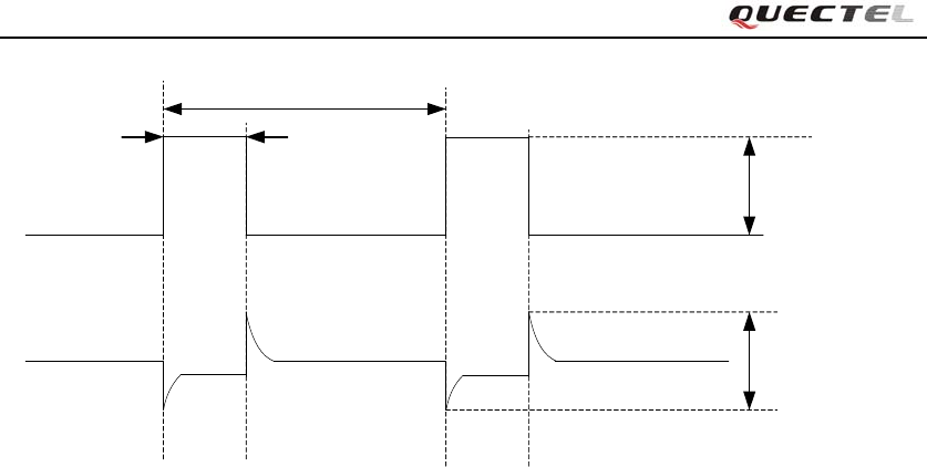
The RF Power Amplifier current (1.6A peak in GSM/GPRS mode) flows with a ratio of 1/8 of
time, around 577us every 4.615ms, in talking mode. The following figure is the VBAT voltage
and current ripple at the maximum power transmitting phase, the test condition is VBAT=4.16V,
VBAT maximum output current is 1.6A, C3=100µF tantalum capacitor (ESR=0.7Ω).
M10 Hardware Design
M10_HD_V3.0 - 27 -
Max:400mV
4.615ms
577us
IBAT
VBAT
Burst:1.6A
Figure 4: Ripple in supply voltage during transmitting burst
3.3.1. Power supply pins
The VBAT pins are dedicated to connect the module supply voltage. VRTC pin can be used to
connect a rechargeable coin battery or a golden capacitor which can help to maintain the system
clock when VBAT supply is not applied.
3.3.2. Minimizing supply voltage drop
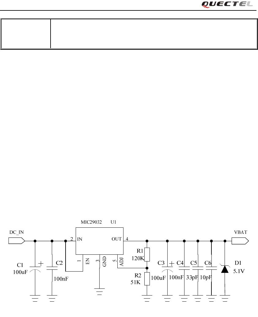
Please pay special attention to the power supply design for your applications. Make sure that the
input voltage will never drop below 3.3V even in a transmitting burst during which the current
consumption may rise up to 1.6A. If the power voltage drops below 3.3V, the module could turn
off automatically. The PCB traces from the VBAT pads to the power source must be wide enough
to ensure that there is not too much voltage drop occur in the transmitting burst mode. The width
of trace should be no less than 2mm and the principle of the VBAT trace is the longer route, the
wider trace. The VBAT voltage can be measured by oscilloscope.
For the VBAT input, a bypass capacitor of about 100 µF with low ESR is recommended.
Multi-layer ceramic chip (MLCC) capacitor can provide the best combination of low ESR and
small size but may not be economical. A lower cost choice could be a 100 µF tantalum capacitor
with low ESR. Other small ceramic capacitors should be in parallel with the 100µF capacitor,
which is illustrated in Figure 5. The capacitors should be placed close to the M12 VBAT pins.
M10 Hardware Design
M10_HD_V3.0 - 28 -
C1>=100uF; C2=0.1uF~1uF; C3=10pF; C4=33pF
Figure 5: Reference circuit of the VBAT input
3.3.3. Monitor power supply
To monitor the supply voltage, you can use the “AT+CBC” command which includes three
parameters: charging status, remaining battery capacity and voltage value (in mV). It returns the
0-100 percent of battery capacity and actual value measured between VBAT and GND. The
voltage is continuously measured at an interval depending on the operating mode. The displayed
voltage (in mV) is averaged over the last measuring period before the “AT+CBC” command is
executed.
For details, please refer to document [1].
3.4. Power up and down scenarios
3.4.1. Power on
The module can be turned on through the two ways, which are described in following chapters:
Via PWRKEY pin: start normal operating mode (please refer to chapter 3.4.1.1);
Via RTC interrupt: start ALARM mode (please refer to chapter 3.4.1.2).
Note: The module is set to autobauding mode (AT+IPR=0) in default configuration. In the
autobauding mode, the URC “RDY” is not sent to host controller after powering on. AT
command can be sent to the module 2-3 seconds after the module is powered on. Host controller
should firstly send an “AT” or “at” string in order that the module can detect baud rate of host
controller, and it should send the second or the third “AT” or “at” string until receiving “OK”
string from module. Then an “AT+IPR=x;&W” should be sent to set a fixed baud rate for
M10 Hardware Design
M10_HD_V3.0 - 29 -
module and save the configuration to flash memory of module. After these configurations, the
URC “RDY” would be received from the Serial Port of module every time when the module is
powered on. Refer to Chapter “AT+IPR” in document [1].
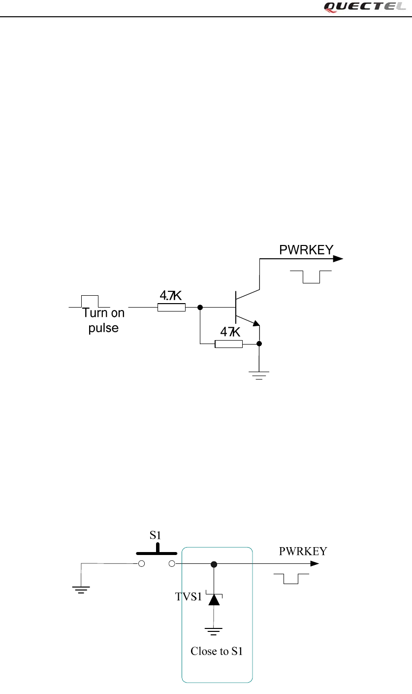
3.4.1.1. Power on module using the PWRKEY pin
Customer’s application can turn on the module by driving the pin PWRKEY to a low level voltage
and after STATUS pin outputs a high level, PWRKEY pin can be released. Customer may
monitor the level of the STATUS pin to judge whether the module is power-on or not. An open
collector driver circuit is suggested to control the PWRKEY. A simple reference circuit is
illustrated in Figure 6.
Figure 6: Turn on the module using driving circuit
The other way to control the PWRKEY is using a button directly. A TVS component is
indispensable to be placed nearby the button for ESD protection. When pressing the key,
electrostatic strike may generate from finger. A reference circuit is showed in Figure 7.
Figure 7: Turn on the module using keystroke
M10 Hardware Design
M10_HD_V3.0 - 30 -
The power on scenarios is illustrated as following figure.
VDD_EXT
(OUTPUT)
VIL<0.1*VBAT
VIH > 0.6*VBAT
VBAT
PWRKEY
(INPUT)
EMERG_OFF
(INPUT)
54ms
STATUS
(OUTPUT)
800ms
>1s
OFF BOOTING
MODULE
STATUS RUNNING
2
1
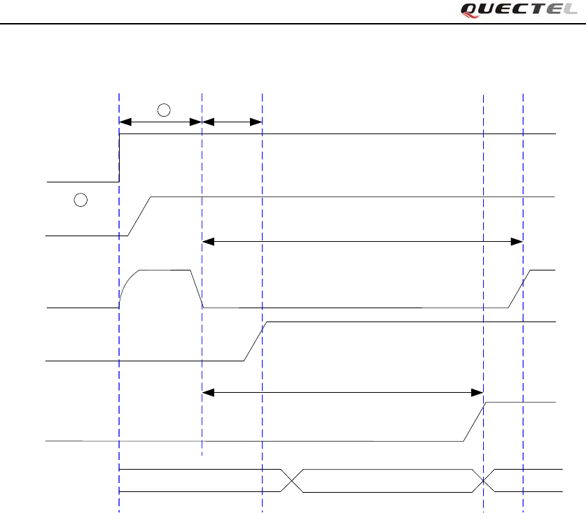
Figure 8: Timing of turning on system
① Make sure that VBAT voltage is stable before pulling down PWRKEY pin. The interval time
between them is recommended 30ms.
② Keep the EMERG_OFF pin open if not used.
Note: Customer can monitor the voltage level of the STATUS pin to judge whether the module
is power-on. After the STATUS pin goes to high level, PWRKEY may be released. If the
STATUS pin is ignored, pull the PWRKEY pin to low level for more than 2 seconds to turn on
the module.
3.4.1.2. Power on module using the RTC (Alarm mode)
Alarm mode is a power-on approach by using the RTC. The alert function of RTC can wake-up
the module while it is in power-off state. In alarm mode, the module will not register to GSM
network and the GSM protocol stack software is closed. Thus the part of AT commands related
with SIM card and the protocol stack will not be accessible, and the others can be used.
Use the “AT+QALARM” command to set the alarm time. The RTC remains the alarm time if the
module is powered off by “AT+QPOWD=1” or by PWRKEY pin. Once the alarm time is expired,

M10 Hardware Design
M10_HD_V3.0 - 31 -
the module will go into the alarm mode. In this case, the module will send out an Unsolicited
Result Code (URC) when the baud rate of the Serial Port is set to a fixed one.
RDY
ALARM MODE
+CFUN:0
Note: This result code does not appear when autobauding is active because a valid baud rate is
not available immediately after powering up the module. Therefore, the module is
recommended to set to a fixed baud rate.
During alarm mode, use “AT+CFUN” command to query the status of software protocol stack; it
will return “0” which indicates that the protocol stack is closed. After 90 seconds, the module will
power down automatically. However, if the GSM protocol stack is started by “AT+CFUN=1”
command during the alarm mode, the process of automatic power-off will not be executed. In
alarm mode, driving the PWRKEY to a low level voltage for a period will cause the module to
power down.
The frequently-used AT commands during alarm mode are briefly summarized In Table 7. For
details of these instructions, please refer to document [1].
Table 7: AT commands used in alarm mode
AT command Function
AT+QALARM Set alarm time
AT+CCLK Set data and time of RTC
AT+QPOWD Power down the module
AT+CFUN Start or close the protocol stack
3.4.2. Power down
The following procedures can be used to turn off the module:
Normal power down procedure: Turn off module using the PWRKEY pin
Normal power down procedure: Turn off module using command “AT+QPOWD”
Over-voltage or under-voltage automatic shutdown: Take effect when over-voltage or
under-voltage is detected
Emergent power down procedure: Turn off module using the EMERG_OFF pin
M10 Hardware Design
M10_HD_V3.0 - 32 -
3.4.2.1. Power down module using the PWRKEY pin
Customer’s application can turn off the module by driving the PWRKEY to a low level voltage for
certain time. The power-down scenario is illustrated as in Figure 9.
The power-down procedure causes the module to log off from the network and allows the
software to save important data before completely disconnecting the power supply, thus it is a safe
way.
Before the completion of the power-down procedure, the module sends out the result code as
shown below:
NORMAL POWER DOWN
Note: This result code does not appear when autobauding is active and DTE and DCE are not
correctly synchronized after start-up. The module is recommended to set a fixed baud rate.
After this moment, no other AT commands can be executed. And then the module enters the
POWER DOWN mode, only the RTC is still active. The POWER DOWN mode can also be
indicated by the STATUS pin, which is a low level voltage in this mode.
VBAT
PWRKEY
(INPUT)
STATUS
(OUTPUT)
EMERG_OFF
(INPUT)
Logout net about 2s to 12s
0.6s<Pulldown<1s >160us
Figure 9: Timing of turning off the module
3.4.2.2. Power down module using AT command
Customer’s application can use an AT command “AT+QPOWD=1” to turn off the module. This
command will let the module to log off from the network and allow the software to save important

M10 Hardware Design
M10_HD_V3.0 - 33 -
data before completely disconnecting the power supply, thus it is a safe way.
Before the completion of the power-down procedure, the module sends out the result code as
shown below:
NORMAL POWER DOWN
After this moment, no other AT commands can be executed. And then the module enters the
POWER DOWN mode, only the RTC is still active. The POWER DOWN mode can also be
indicated by STATUS pin, which is a low level voltage in this mode.
For details about the AT command of “AT+QPOWD”, please refer to document [1].
3.4.2.3. Over-voltage or under-voltage automatic shutdown
The module will constantly monitor the voltage applied on the VBAT, if the voltage is ≤ 3.5V, the
following URC will be presented:
UNDER_VOLTAGE WARNING
If the voltage is ≥ 4.5V, the following URC will be presented:
OVER_VOLTAGE WARNING
The normal input voltage range is 3.3V to 4.6V. If the voltage is > 4.6V or <3.3V, the module
would automatically shutdown itself.
If the voltage is <3.3V, the following URC will be presented:
UNDER_VOLTAGE POWER DOWN
If the voltage is >4.6V, the following URC will be presented:
OVER_VOLTAGE POWER DOWN
Note: These result codes don’t appear when autobauding is active and DTE and DCE are not
correctly synchronized after start-up. The module is recommended to set to a fixed baud rate.
After this moment, no other AT command can be executed, the module logs off from network and
enters POWER DOWN mode, and only RTC is still active. The POWER DOWN mode can also
be indicated by the pin STATUS, which is a low level voltage in this mode.
M10 Hardware Design
M10_HD_V3.0 - 34 -
3.4.2.4. Emergency shutdown
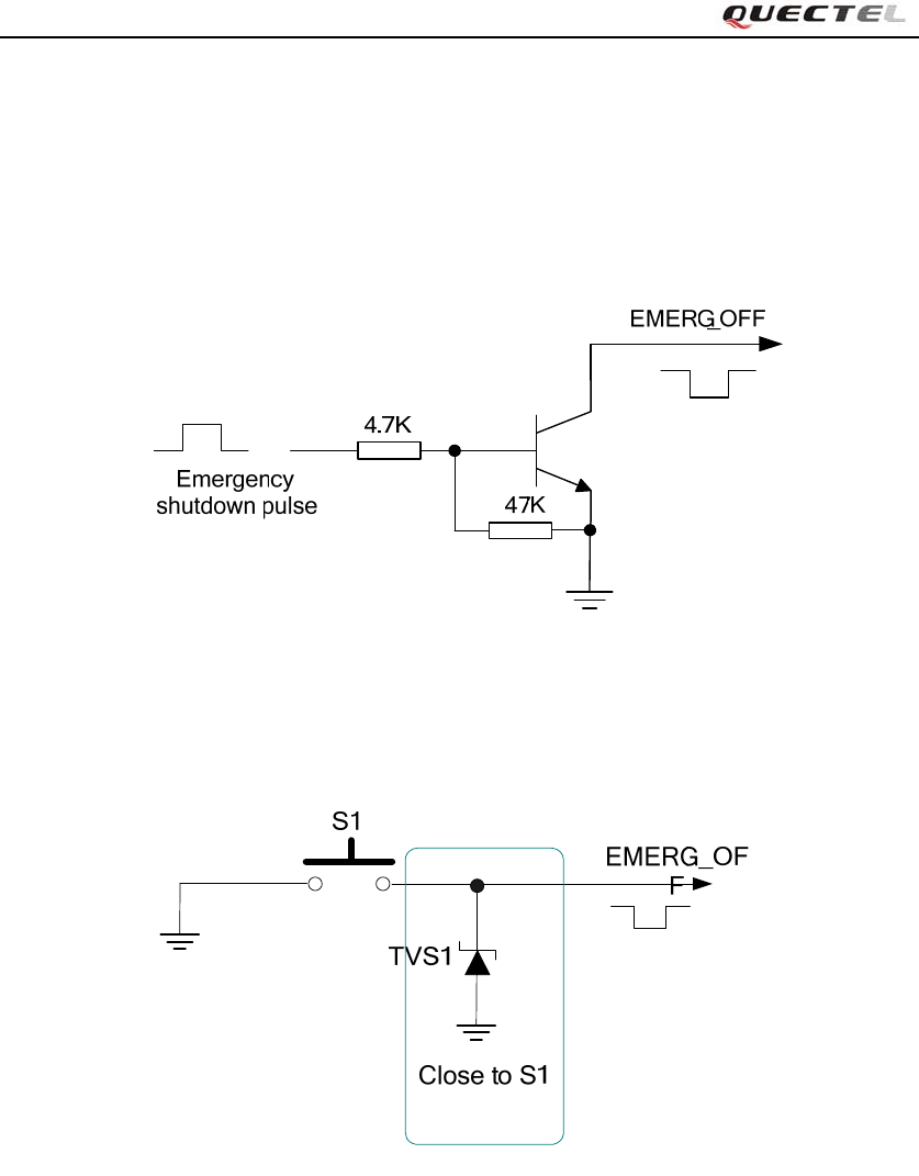
The module can be shut down by driving the pin EMERG_OFF to a low level voltage for over 20ms
and then releasing it. The EMERG_OFF line can be driven by an Open Drain/Collector driver or a
button. The circuit is illustrated as the following figures.
Figure 10: Reference circuit for EMERG_OFF by using driving circuit
Figure 11: Reference circuit for EMERG_OFF by using button
Be cautious to use the pin EMERG_OFF. It should only be used under emergent situation. For
instance, if the module is unresponsive or abnormal, the pin EMERG_OFF could be used to
shutdown the system. Although turning off the module by EMERG_OFF is fully tested and nothing
wrong is detected, this operation is still a big risk as it could cause destroying of the code or data
area of the NOR flash memory in the module. Therefore, it is recommended that PWRKEY or AT
command should always be the preferential way to turn off the system.
M10 Hardware Design
M10_HD_V3.0 - 35 -
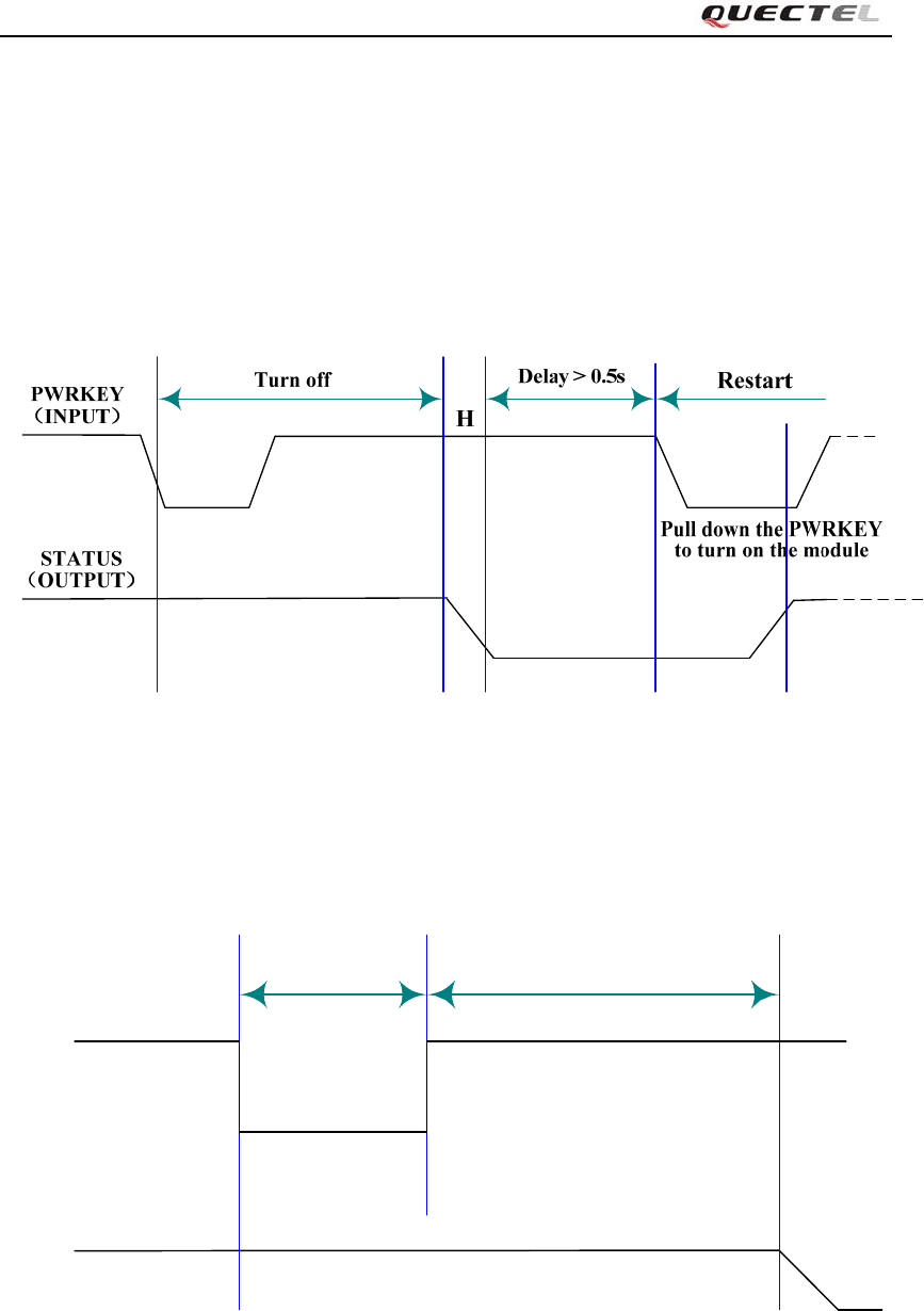
3.4.3. Restart module using the PWRKEY pin
Customer’s application can restart the module by driving the PWRKEY to a low level voltage for
certain time, which is similar to the way to turn on the module. Before restarting the module, at least
500ms should be delayed after detecting the low level of STATUS. The restart scenario is illustrated
as the following figure.
Figure 12: Timing of restarting system
The module can also be restarted by the PWRKEY after emergency shutdown.
PWRKEY
(INPUT)
Pulldown >20ms Delay>2s
EMERG_OFF
(INPUT)
Figure 13: Timing of restarting system after emergency shutdown

M10 Hardware Design
M10_HD_V3.0 - 36 -
3.5. Power saving
Upon system requirement, there are several actions to drive the module to enter low current
consumption status. For example, “AT+CFUN” can be used to set the module into minimum
functionality mode and DTR hardware interface signal can be used to lead system to SLEEP
mode.
3.5.1. Minimum functionality mode
Minimum functionality mode reduces the functionality of the module to minimum level, thus
minimizes the current consumption when the slow clocking mode is activated at the same time.
This mode is set with the “AT+CFUN” command which provides the choice of the functionality
levels <fun>=0,1,4.
0: minimum functionality
1: full functionality (default)
4: disable both transmitting and receiving of RF part
If the module is set to minimum functionality by “AT+CFUN=0”, the RF function and SIM card
function would be closed. In this case, the serial port is still accessible, but all AT commands
correlative with RF function or SIM card function will not be accessible.
If the module has been set by “AT+CFUN=4”, the RF function will be closed but the serial port is
still active. In this case, all AT commands correlative with RF function will not be accessible.
After the module is set by “AT+CFUN=0” or “AT+CFUN=4”, it can return to full functionality by
“AT+CFUN=1”.
For detailed information about “AT+CFUN”, please refer to document [1].
3.5.2. SLEEP mode (slow clock mode)
The SLEEP mode is disabled in default software configuration. Customer’s application can enable
this mode by “AT+QSCLK=1”. On the other hand, the default setting is “AT+QSCLK=0” and in
this mode, the module cannot enter SLEEP mode.
When “AT+QSCLK=1” is set to the module, customer’s application can control the module to
enter or exit from the SLEEP mode through pin DTR. When DTR is set to high level, and there is
no on-air or hardware interrupt such as GPIO interrupt or data on serial port, the module will enter
SLEEP mode automatically. In this mode, the module can still receive voice, SMS or GPRS
paging from network but the serial port is not accessible.

M10 Hardware Design
M10_HD_V3.0 - 37 -
3.5.3. Wake up module from SLEEP mode
When the module is in the SLEEP mode, the following methods can wake up the module.
If the DTR Pin is pulled down to a low level, it would wake up the module from the SLEEP mode.
The serial port will be active about 20ms after DTR is changed to low level.
Receive a voice or data call from network to wake up module.
Receive an SMS from network to wake up module.
RTC alarm expired to wake up module.
Note: DTR pin should be held low level during communicating between the module and DTE.
3.6. Summary of state transitions (except SLEEP mode)
Table 8: Summary of state transition
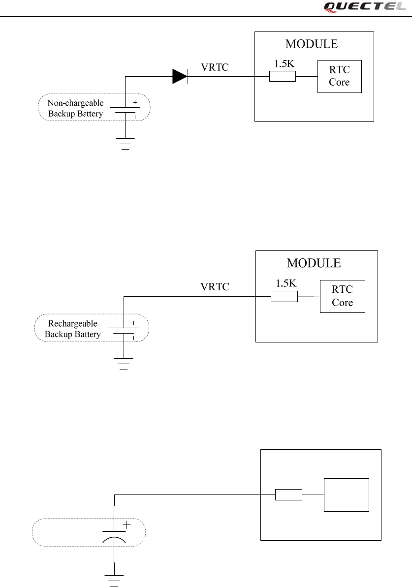
3.7. RTC backup
The RTC (Real Time Clock) can be supplied by an external capacitor or battery (rechargeable or
non-chargeable) through the pin VRTC. A 1.5K resistor has been integrated in the module for
current limiting. A coin-cell battery or a super-cap can be used to backup power supply for RTC.
The following figures show various sample circuits for RTC backup.
Current mode Next mode
POWER DOWN Normal mode Alarm mode
POWER DOWN Use PWRKEY Turn on the module by RTC
alarm
Normal mode Use “AT+QPOWD”
command, PWRKEY
pin, or EMERG_OFF
pin
Set alarm by “AT+QALARM”,
and then turn off the module.
When the timer expires, the
module turns on automatically
and enters Alarm mode.
Alarm mode Use PWRKEY pin or
wait module turning
off automatically
Use
“AT+CFUN”
command
M10 Hardware Design
M10_HD_V3.0 - 38 -
Figure 14: RTC supply from non-chargeable battery
Figure 15: RTC supply from rechargeable battery
VRTC
Large Capacitance
Capacitor
MODULE
RTC
Core
1.5K
Figure 16: RTC supply from capacitor
Coin-type rechargeable capacitor such as XH414H-IV01E from Seiko can be used.
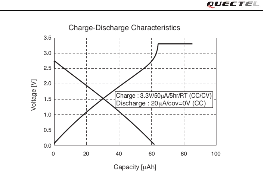
M10 Hardware Design
M10_HD_V3.0 - 39 -
Figure 17: Seiko XH414H-IV01E Charge Characteristic
3.8. Serial interfaces
The module provides two unbalanced asynchronous serial ports including Serial Port, Debug Port.
The module is designed as a DCE (Data Communication Equipment), following the traditional
DCE-DTE (Data Terminal Equipment) connection. Autobauding function supports baud rate from
4800bps to 115200bps.
The UART Port:
TXD: Send data to RXD of DTE
RXD: Receive data from TXD of DTE
RTS: Requests to send
CTS: Clear to send
DTR: DTE is ready and inform DCE (this pin can wake the module up)
RI: Ring indicator (when the call, SMS, data of the module are coming, the module will
output signal to inform DTE)
DCD: Data carrier detection (the validity of this pin demonstrates the communication link is
set up)
Note: The module disables hardware flow control by default. When hardware flow control is
required, RTS and CTS should be connected to the host. AT command “AT+IFC=2,2” is used to
enable hardware flow control. AT command “AT+IFC=0,0” is used to disable the hardware
flow control. For more details, please refer to document [1].
M10 Hardware Design
M10_HD_V3.0 - 40 -
The Debug Port:
DBG_TXD: Send data to the COM port of a debugging computer
DBG_RXD: Receive data from the COM port of a debugging computer
UART3:
TXD_AUX: Send data to the RXD of DTE
RXD_AUX: Receive data from the TXD of DTE
The logic levels are described in the following table.
Table 9: Logic levels of the serial interface
Table 10: Pin definition of the serial interfaces
Interface Name Pin Function
Debug Port DBG_RXD 9 Receive data of the debug port
DBG_TXD 10 Transmit data of the debug port
Serial Port
RI 55 Ring indicator
RTS 58 Request to send
CTS 57 Clear to send
RXD 61 Receive data of the serial port
TXD 60 Transmit data of the serial port
DTR 59 Data terminal ready
DCD 56 Data carrier detection
UART3 TXD3 62 Transmit data of UART3
RXD3 63 Receive data of UART3
3.8.1. UART Port
3.8.1.1. The features of UART Port.
Seven lines on UART interface:
Contain data lines TXD and RXD, hardware flow control lines RTS and CTS, other control
lines DTR, DCD and RI.
Parameter Min Max Unit
VIL 0 0.25*VDD_EXT V
VIH 0.75*VDD_EXT VDD_EXT +0.3 V
VOL 0 0.15*VDD_EXT V
VOH 0.85*VDD_EXT VDD_EXT V

M10 Hardware Design
M10_HD_V3.0 - 41 -
The module disables hardware flow control in default, AT command “AT+IFC=2,2” is used
to enable hardware flow control.
Used for AT command, GPRS data, CSD FAX, etc. Multiplexing function is supported on the
UART Port. So far only the basic mode of multiplexing is available.
Support the communication baud rates as the following:
300,600,1200,2400,4800,9600,14400,19200,28800,38400,57600,115200.
The default setting is autobauding mode. Support the following baud rates for Autobauding
function: 4800, 9600, 19200, 38400, 57600, 115200.
After setting a fixed baud rate or Autobauding, please send “AT” or “at” string at that rate. The
UART port is ready when it responds with “OK”.
Autobauding allows the module to detect the baud rate by receiving the string “AT” or “at” from
the host or PC automatically, which gives module flexibility without considering which baud rate
is used by the host controller. Autobauding is enabled by default. To take advantage of the
autobauding mode, special attention should be paid according to the following requirements:
Synchronization between DTE and DCE:
When DCE (the module) powers on with the autobauding enabled, it is recommended to wait 2 to
3 seconds before sending the first “AT” string. After receiving the “OK” response, DTE and DCE
are correctly synchronized.
If the host controller needs URC in the mode of autobauding, it must be synchronized first.
Otherwise the URC will be discarded.
Restrictions on autobauding operation
The UART port has to be operated at 8 data bits, no parity and 1 stop bit (factory setting).
The A/ and a/ commands can’t be used.
Only the strings “AT” or “at” can be detected (neither “At” nor “aT”).
The Unsolicited Result Codes like “RDY”, “+CFUN: 1” and “+CPIN: READY” will not be
indicated when the module is turned on with autobauding enabled and not be synchronized.
Any other Unsolicited Result Codes will be sent at the previous baud rate before the module
detects the new baud rate by receiving the first “AT” or “at” string. The DTE may receive
unknown characters after switching to new baud rate.
It is not recommended to switch to autobauding from a fixed baud rate.
If autobauding is active it is not recommended to switch to multiplex mode
Note: To assure reliable communication and avoid any problems caused by undetermined baud
rate between DCE and DTE, it is strongly recommended to configure a fixed baud rate and save
it instead of using autobauding after start-up. For more details, please refer to Section
“AT+IPR” in document [1].
M10 Hardware Design
M10_HD_V3.0 - 42 -
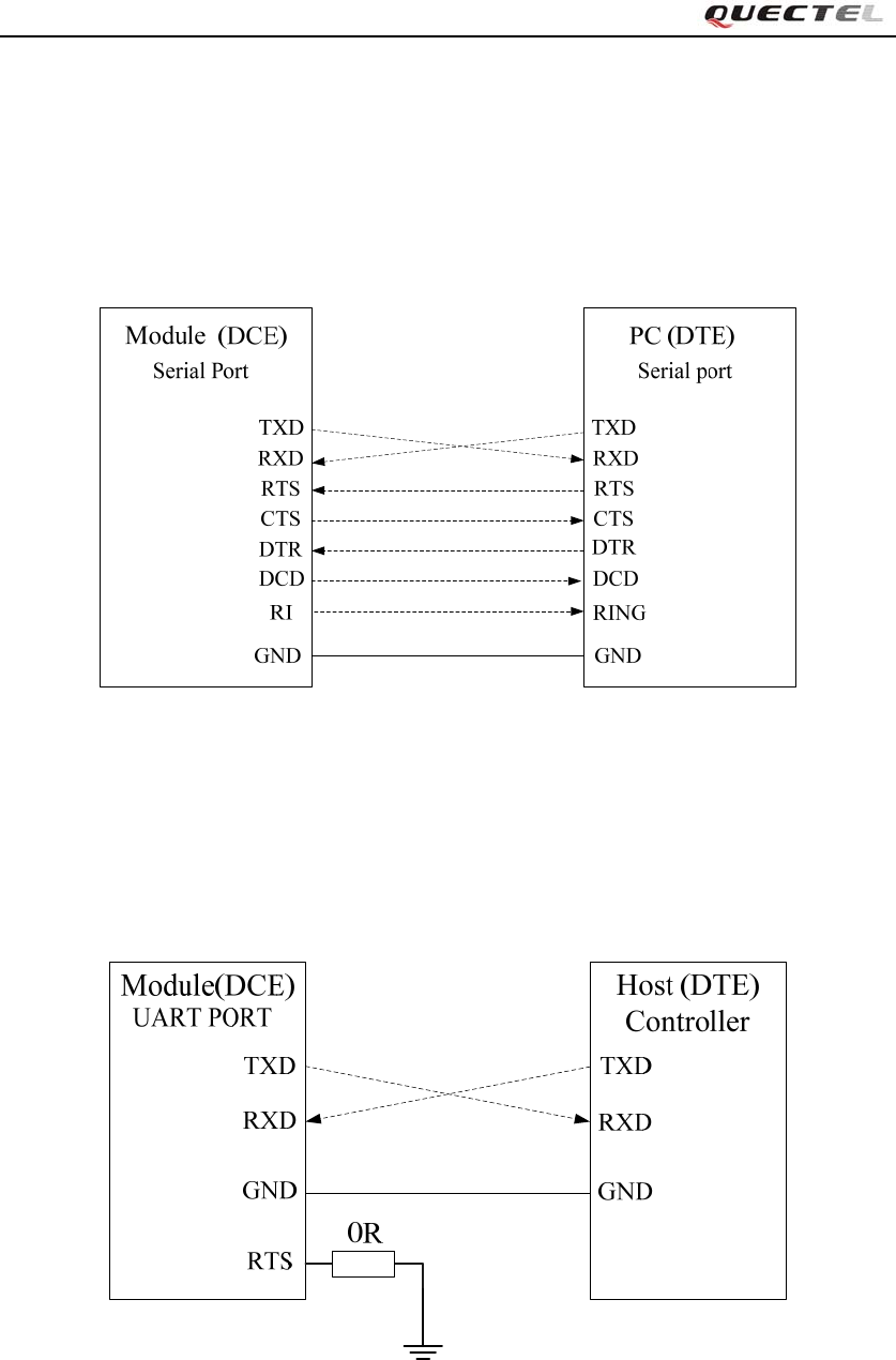
3.8.1.2. The connection of UART
The connection between module and host via UART port is very flexible. Three connection styles
are illustrated as below.
UART Port connection is shown as below when it is applied in modulation-demodulation.
Figure 18: Connection of all functional UART port
Three lines connection is shown as below.
Figure 19: Connection of three lines UART port
UART Port with hardware flow control is shown as below. This connection will enhance the

M10 Hardware Design
M10_HD_V3.0 - 43 -
reliability of the mass data communication.
Figure 20: Connection of UART port with hardware flow control
3.8.1.3. Software upgrade
The TXD and RXD can be used to upgrade software. The PWRKEY pin must be pulled down
before the software upgrade. Please refer to the following figure for software upgrade.
IO Connector
TXD
RXD
GND
PWRKEY
Module (DCE)
UART port
TXD
RXD
GND
PWRKEY
Figure 21: Connection of software upgrade
3.8.2. Debug Port
Debug Port:
Two lines: DBG_TXD and DBG_RXD
It outputs log information automatically.
Debug Port is only used for software debugging and its baud rate must be configured as
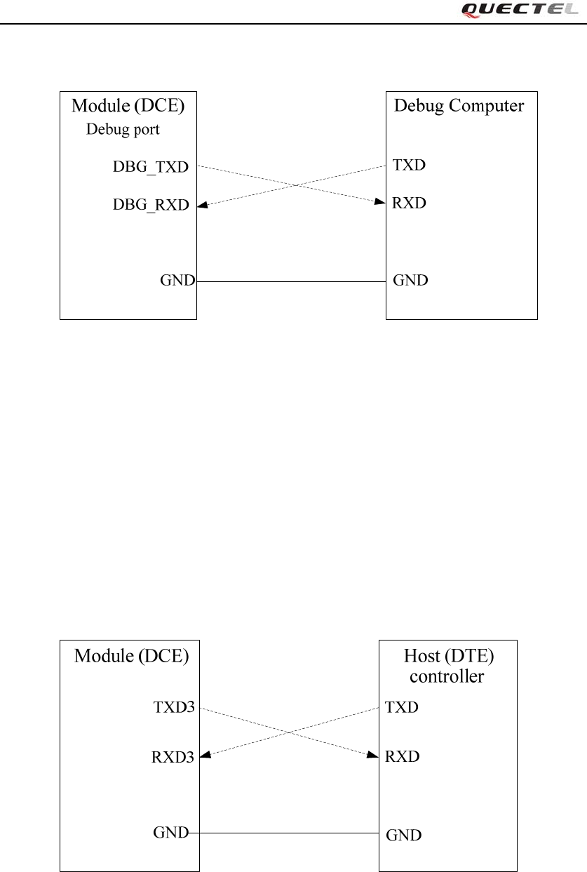
M10 Hardware Design
M10_HD_V3.0 - 44 -
460800bps.
Figure 22: Connection of software debug
3.8.3. UART Port 3
UART3:
Two data lines: TXD3and RXD3
UART3 port is used for AT command only and does not support GPRS data, CSD FAX,
Multiplexing function etc.
Support the communication baud rates as the following:
4800, 9600, 14400, 19200,28800,38400,57600,115200.
The default baud rate setting is 115200bps, and does not support autobauding. The baud rate
can be modified by AT+QSEDCB command. For more details, please refer to document [1].
Figure 23: Connection of Auxiliary UART port
M10 Hardware Design
M10_HD_V3.0 - 45 -
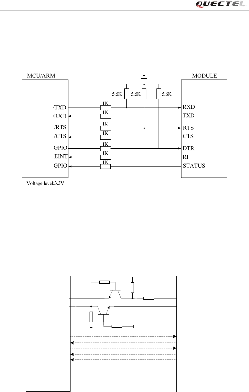
3.8.4. UART Application
The reference design of 3.3V level match is shown as below. When the peripheral MCU/ARM
system is 3V, the divider resistor should be changed from 5.6K to 10K.
Figure 24: 3.3V level match circuit
The reference design of 5V level match is shown as below. The construction of dotted line can
refer to the construction of solid line. Please pay attention to direction of connection. Input dotted
line of module should refer to input solid line of the module. Output dotted line of module should
refer to output solid line of the module.
MCU/ARM
/TXD
/RXD
1K
VDD_EXT
4.7k
VCC_MCU
4.7k
4.7k
4.7k
VDD_EXT
TXD
RXD
RTS
CTS
DTR
RI
/RTS
/CTS
GND
VBAT
GPIO STATUS
MODULE
GPIO
EINT
VCC_MCU
Voltage level: 5V
Figure 25: 5V level match circuit
M10 Hardware Design
M10_HD_V3.0 - 46 -
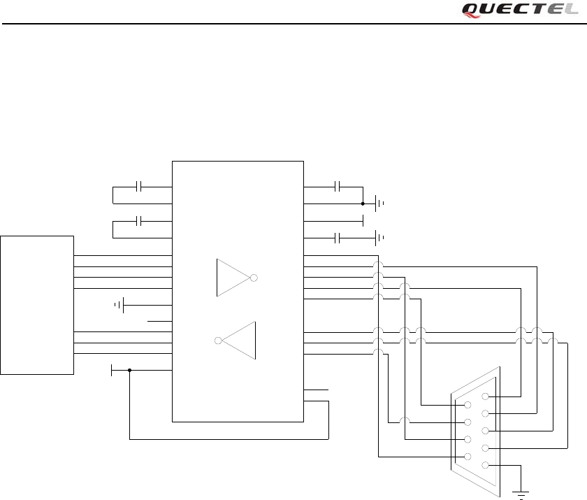
The following picture is an example of connection between module and PC. A RS_232 level
shifter IC or circuit must be inserted between module and PC, since these three UART ports do
not support the RS_232 level, while support the CMOS level only.
9
8
7
6
5
4
3
2
1
15
14
8
9
11
12
5
7
6
10
4
26
2
27
13
18
20
21
16
17
19
22
23
24
3
1
25
28
GND
TO PC serial port
SP3238
3V
GND
GND
T5OUT
/SHUTDOWN
V+
GND
V-
VCC
T4OUT
T2OUT
T3OUT
T1OUT
R3IN
R2IN
R1IN
/STATUS
3V ONLINE
R1OUT
R2OUT
R3OUT
/R1OUT
GND T5IN
T4IN
T3IN
T2IN
T1IN
C2+
C2-
C1-
C1+
MODULE
RXD
DTR
RTS
RI
CTS
TXD
DCD
Figure 26: RS232 level match circuit
3.9. Audio interfaces
The module provides two analogy input channels and two analogy output channels.
M10 Hardware Design
M10_HD_V3.0 - 47 -
Table 11: Pin definition of Audio interface
AIN1 and AIN2, which may be used for both microphone and line inputs. An electret
microphone is usually used. AIN1 and AIN2 are both differential input channels.
AOUT1 and AOUT2, which may be used for both receiver and speaker outputs. AOUT1
channel is typically used for a receiver built into a handset, while AOUT2 channel is typically
used with headset or hands-free speaker. AOUT1 channel is a differential channel and
AOUT2 is a single-ended channel. SPK2P and AGND can establish a pseudo differential
mode. If customer needs to play Melody or Midi ringtone for incoming call, AOUT2 Channel
should always be used.
These two audio channels can be swapped by “AT+QAUDCH” command. For more details,
please refer to document [1].
Use AT command “AT+QAUDCH” to select audio channel:
0--AIN1/AOUT1 (normal audio channel), the default value is 0.
1--AIN2/AOUT2 (aux audio channel).
For each channel, customer can use AT+QMIC to adjust the input gain level of microphone.
Customer can also use “AT+CLVL” to adjust the output gain level of receiver and speaker.
“AT+QECHO” is to set the parameters for echo cancellation control. “AT+QSIDET” is to set the
side-tone gain level. For more details, please refer to document [1].
3.9.1. Decrease TDD noise and other noise
The 33pF capacitor is applied for filtering out 850MHz/900MHz RF interference when the
module is transmitting at GSM900MHz. Without placing this capacitor, TDD noise could be
heard. Moreover, the 10pF capacitor here is for filtering out 1800MHz/1900MHz RF interference.
However, the resonant frequency point of a capacitor largely depends on the material and
production technique. Therefore, customer would have to discuss with its capacitor vendor to
choose the most suitable capacitor for filtering out GSM850MHz, GSM900MHz, DCS1800MHz
and PCS1900MHz separately.
Interface Name Pin Function
(AIN1/AOUT1)
MIC1P 23 Microphone1 input +
MIC1N 24 Microphone1 input -
SPK1P 22 Audio1 output+
SPK1N 21 Audio1 output-
(AIN2/AOUT2)
MIC2P 25 Microphone2 input +
MIC2N 26 Microphone2 input -
SPK2P 20 Audio2 output+
AGND 19 Suggested to be used in audio circuit. Do not
connect to digital GND in host PCB as it could
produce TDD noise.
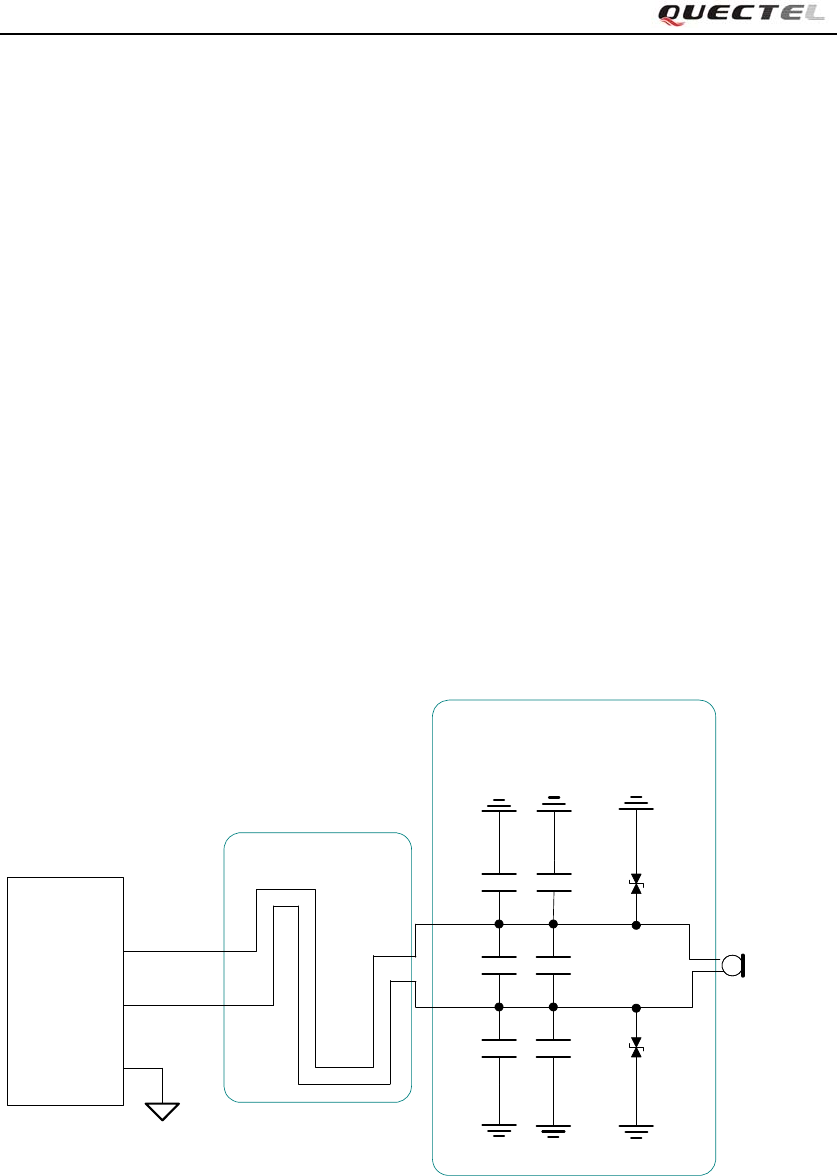
M10 Hardware Design
M10_HD_V3.0 - 48 -
The severity degree of the RF interference in the voice channel during GSM transmitting period
largely depends on the application design. In some cases, GSM850/GSM900 TDD noise is more
severe; while in other cases, DCS1800/PCS1900 TDD noise is more obvious. Therefore, customer
can have a choice based on test results. Sometimes, even no RF filtering capacitor is required.
The capacitor which is used for filtering out RF noise should be close to RJ11 or other audio
interfaces. Audio alignment should be as short as possible.
In order to decrease radio or other signal interference, the position of RF antenna should be kept
away from audio interface and audio alignment. Power alignment and audio alignment should not
be parallel, and power alignment should be far away from audio alignment.
The differential audio traces have to be placed according to the differential signal layout rules.
3.9.2. Microphone interfaces configuration
AIN1/IN2 channels come with internal bias supply for external electret microphone. A reference
circuit is shown in Figure27.
10pF 33pF
33pF
33pF
Close to Microphone
MICxP
MICxN
GND
GND
Differential layout
Module Electret
Microphone
GND
GND
10pF
10pF
GND
GND
ESD
ESD
AGND
Figure 27: Microphone interface configuration of AIN1&AIN2
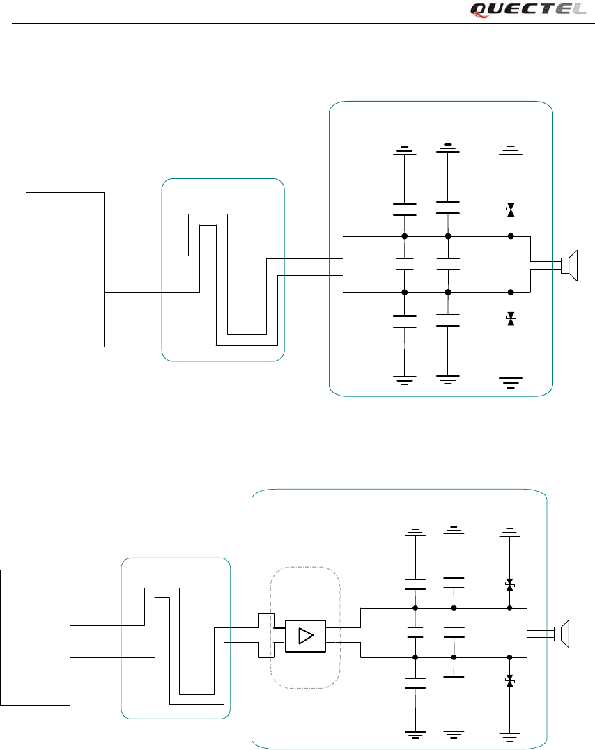
M10 Hardware Design
M10_HD_V3.0 - 49 -
3.9.3. Receiver and speaker interface configuration
SPK1P
SPK1N
Differential layout
10pF
10pF
33pF
33pF
33pF
Close to speaker
GND
GND
10pF
ESD
ESD
Module
Figure 28: Speaker interface configuration of AOUT1
SPK1P
SPK1N
Differential layout Amplifier
circuit 10pF
10pF
33pF
33pF
33pF
Close to speaker
GND
GND
10pF
ESD
ESD
Module
Figure 29: Speaker interface with amplifier configuration of AOUT1
Texas Instruments TPA6205A1is recommended for a suitable differential audio amplifier. There
are plenty of excellent audio amplifiers in the market.
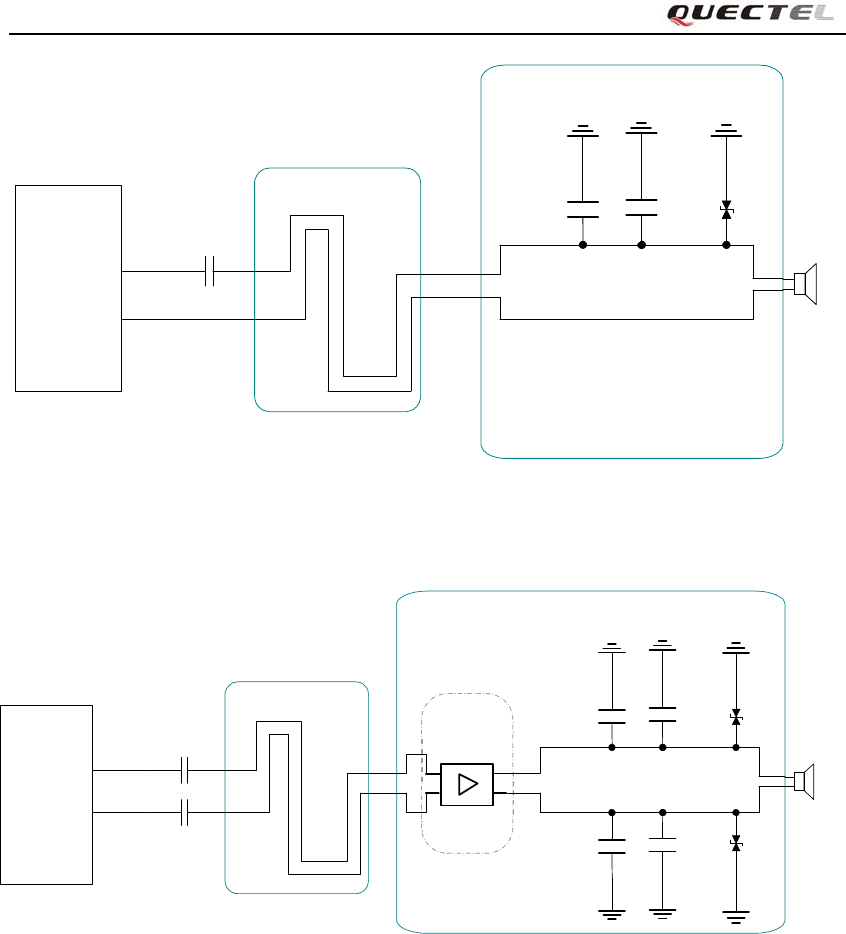
M10 Hardware Design
M10_HD_V3.0 - 50 -
SPK2P
AGND
Differential layout 10pF 33pF
Close to speaker
GND
ESD
Module 22uF
Figure 30: Speaker interface configuration of AOUT2
Module SPK2P
AGND
Differential layout Amplifier
circuit 10pF
10pF 33pF
33pF
Close to speaker
GND
GND
ESD
ESD
C2
C1
Figure 31: Speaker interface with amplifier configuration of AOUT2
Note: The value of C1 and C2 depends on the input impedance of audio amplifier.
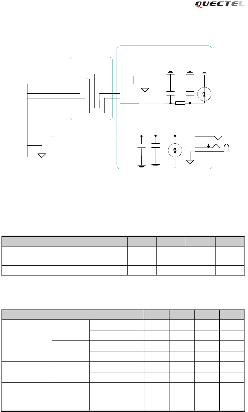
M10 Hardware Design
M10_HD_V3.0 - 51 -
3.9.4. Earphone interface configuration
Amphenol
9001-8905-050
1
2
4
3
SPK2P
MIC2N
MIC2P
22uF
68R
33pF
GND GND
AGND
Close to Socket
Differential layout
33pF
AGND
33pF 10pF
GND GND
GND
GND
AGND
Module
4.7uF
Figure 32: Earphone interface configuration
Table 12: Typical electret microphone characteristic
Parameter Min Type Max Unit
Working Voltage 1.2 1.5 2.0 V
Working Current 200 500 uA
External Microphone Load Resistance 2.2 k Ohm
Table 13: Typical speaker characteristic
Parameter Min Typ Max Unit
Normal
Output(SPK1)
Single
Ended
Load resistance 28 32 Ohm
Ref level 0 2.4 Vpp
Differential Load resistance 28 32 Ohm
Ref level 0 4.8 Vpp
Auxiliary
Output(SPK2)
Single
Ended
Load resistance 16 32 Ohm
Ref level 0 2.4 Vpp
Maxim driving
current limit of
SPK1 and SPK2
50 mA
M10 Hardware Design
M10_HD_V3.0 - 52 -
3.10. SIM card interface
3.10.1. SIM card application
The SIM interface supports the functionality of the GSM Phase 1 specification and also supports
the functionality of the new GSM Phase 2+ specification for FAST 64 kbps SIM card, which is
intended for use with a SIM application Tool-kit.
The SIM interface is powered from an internal regulator in the module. Both 1.8V and 3.0V SIM
Cards are supported.
Table 14: Pin definition of the SIM interface
Figure 33 is the reference circuit for SIM interface, and here an 8-pin SIM card holder is used.
The pin SIM_PRESENCE is used to detect whether the tray of the Molex SIM socket, which is
used for holding SIM card, is present in the card socket. When the tray is inserted in the socket,
SIM_PRESENCE is at low level. Regardless of the SIM card is in the tray or not, the change of
SIM_PRESENCE level from high to low level prompts the module to reinitialize SIM card. In
default configuration, SIM card detection function is disabled. Customer’s application can use
“AT+QSIMDET=1,0 ” to be switched on and “AT+QSIMDET=0,0 ” to switch off the SIM card
detection function. For detail of this AT command, please refer to document [1]. When
“AT+QSIMDET=1,0” is set and the tray with SIM card is removed from SIM socket, the
following URC will be presented.
+CPIN: NOT READY
When the tray with SIM card is inserted into SIM socket again and the module finishes
re-initializing SIM card, the following URC will be presented.
Call Ready
Name Pin Function
SIM_VDD 12 Supply power for SIM Card. Automatic detection of
SIM card voltage. 3.0V±10% and 1.8V±10%.
Maximum supply current is around 10mA.
SIM_DATA 13 SIM Card data I/O
SIM_CLK 14 SIM Card Clock
SIM_RST 15 SIM Card Reset
SIM_PRESENCE 11 SIM Card Presence
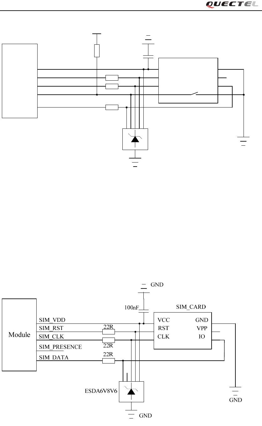
M10 Hardware Design
M10_HD_V3.0 - 53 -
Module
SIM_VDD
SIM_RST
SIM_CLK
SIM_DATA
SIM_PRESENCE
22R
22R
22R
VCC
RST
CLK IO
VPP
GND
VDD_EXT
10K 100nF SIM_CARD
GND
GND
ESDA6V8V6
GNDPRESENCE
Figure 33: Reference circuit of the 8 pins SIM card
Note: Please do not use “AT+QSIMDET=1,1” which causes to initialize SIM card when Figure
33 circuit is adopted.
If customer does not need the SIM card detection function, keep SIM_PRESENCE open. The
reference circuit using a 6-pin SIM card socket is illustrated as the following figure.
Figure 34: Reference circuit of the 6 pins SIM card
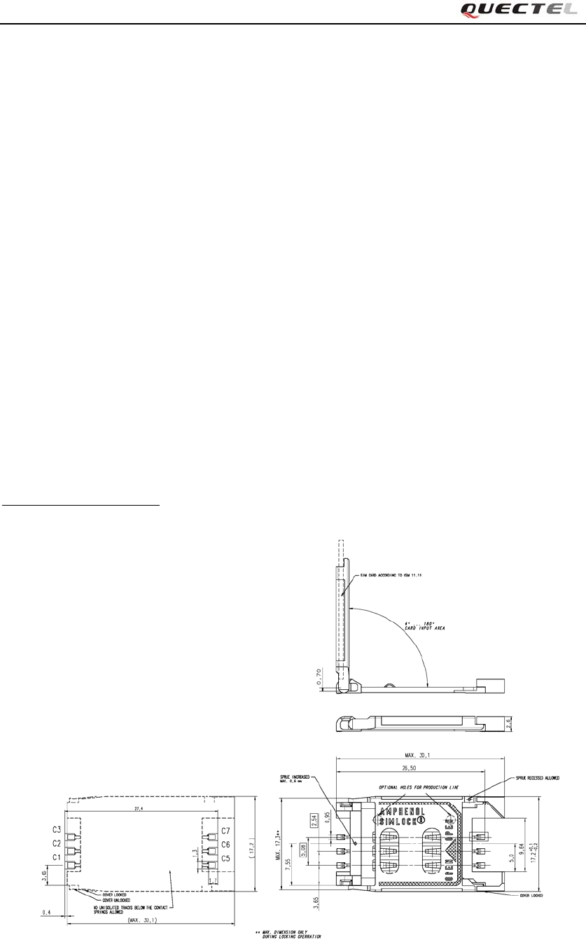
M10 Hardware Design
M10_HD_V3.0 - 54 -
In SIM interface designing, in order to ensure good communication performance with SIM card,
the following design principles should be complied with.
Place the SIM card holder close to module as close as possible. Ensure the trace length of
SIM signals do not exceed 20mm.
Keep the SIM signals far away from VBAT power and RF trace.
The width of SIM_VDD trace is not less than 0.5mm. Place a bypass capacitor close to SIM
card power pin. The value of capacitor is less than 1uF.
To avoid possible cross-talk from the SIM_CLK signal to the SIM_DATA signal be careful
that both lines are not placed closely next to each other. A useful approach is to use GND to
shield the SIM_DATA line from the SIM_CLK line.
In order to ensure good ESD protection, it is recommended to add TVS such as WILL
(http://www.willsemi.com) ESDA6V8AV6. The capacitance of ESD component is less than
50pF. The 22Ω resistors should be added in series between the module and the SIM card so
as to suppress the EMI spurious transmission and enhance the ESD protection. Note that the
SIM peripheral circuit should be close to the SIM card socket.
3.10.2. Design considerations for SIM card holder
For 6-pin SIM card holder, it is recommended to use Amphenol C707 10M006 512 2. Please visit
http://www.amphenol.com for more information.
Figure 35: Amphenol C707 10M006 512 2 SIM card holder
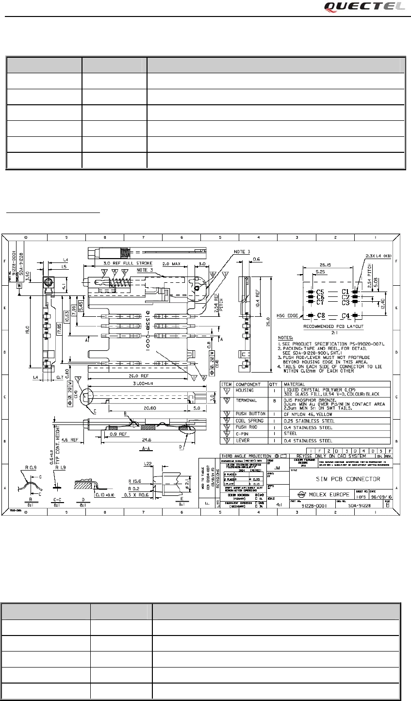
M10 Hardware Design
M10_HD_V3.0 - 55 -
Table 15: Pin description of Amphenol SIM card holder
Name Pin Function
SIM_VDD C1 SIM Card Power supply
SIM_RST C2 SIM Card Reset
SIM_CLK C3 SIM Card Clock
GND C5 Ground
VPP C6 Not Connect
SIM_DATA C7 SIM Card data I/O
For 8-pin SIM card holder, it is recommended to use Molex 91228. Please visit
http://www.molex.com for more information.
Figure 36: Molex 91228 SIM card holder
Table 16: Pin description of Molex SIM card holder
Name Pin Function
SIM_VDD C1 SIM Card Power supply
SIM_RST C2 SIM Card Reset
SIM_CLK C3 SIM Card Clock
SIM_PRESENCE C4 SIM Card Presence Detection
GND C5 Ground
M10 Hardware Design
M10_HD_V3.0 - 56 -
3.11. Keypad interface
The keypad interface consists of 5 keypad column inputs and 5 keypad row outputs. The basic
configuration is 5 keypad columns and 5 keypad rows, giving 25 keys.
Table 17: Pin definition of the keypad interface
The keypad interface allows a direct external matrix connection. A typical recommended circuit
about the keypad is shown in the following figure.
VPP C6 Not Connect
SIM_DATA C7 SIM Card Data I/O
SIM_DETECT C8 Pulled down GND with external circuit. When the tray is
present, C4 is connected to C8.
Name Pin Function
KBC0 33
Keypad matrix column
KBC1 34
KBC2 35
KBC3 36
KBC4 37
KBR0 28
Keypad matrix row
KBR1 29
KBR2 30
KBR3 31
KBR4 32
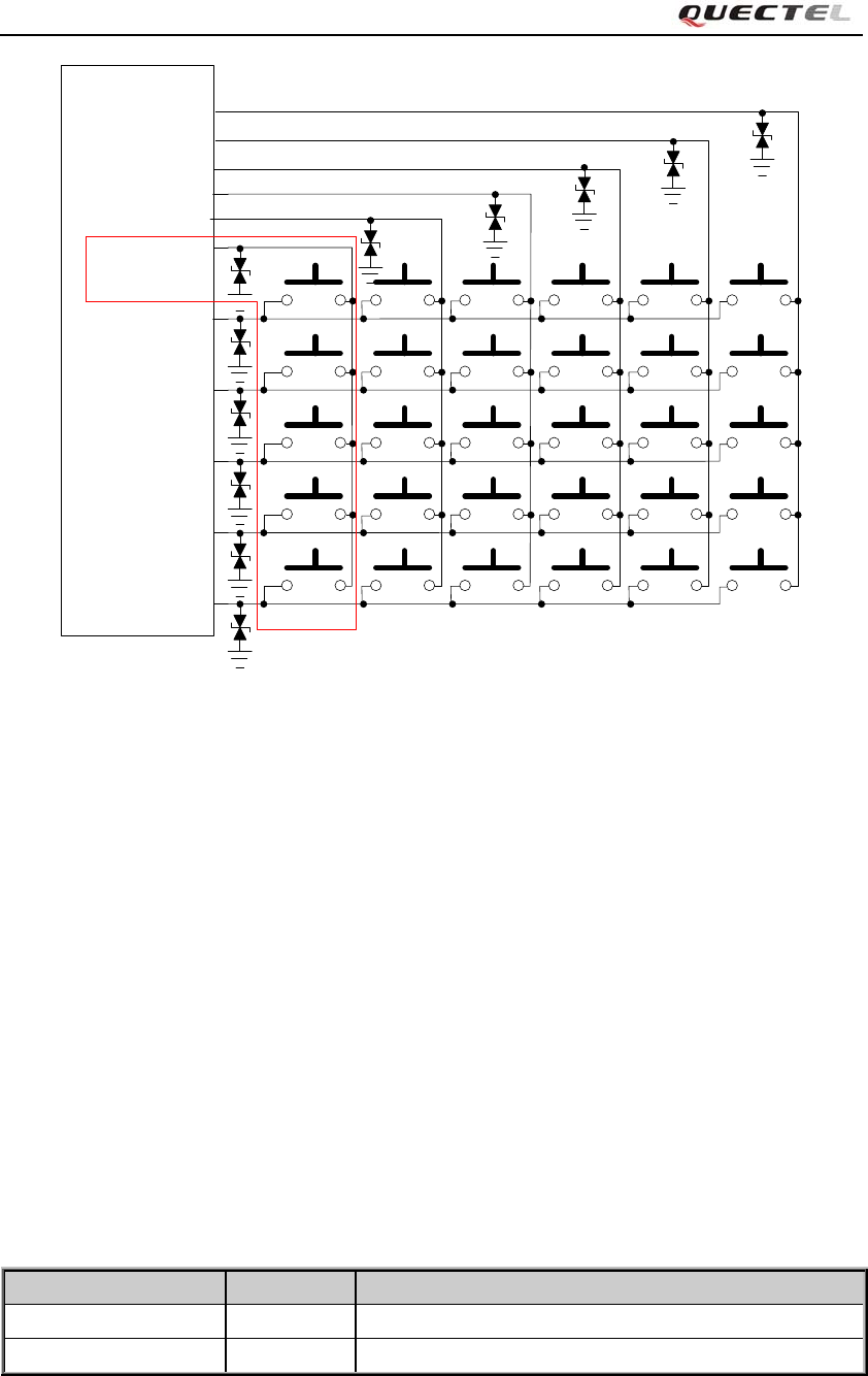
M10 Hardware Design
M10_HD_V3.0 - 57 -
KBR4
KBR3
KBR2
KBR1
KBR0
KBC0
KBC1
KBC2
KBC3
KBC4
Module
GPIO1_KBC5
Figure 37: Reference circuit of the keypad interface
If a 5*5 matrix does not provide enough keys, GPIO1 could be multiplexed as KBC5 to configure
a 5*6 keypad matrix. Then, the keypad interface consists of 5 keypad row outputs and 6 keypad
column inputs. The basic configuration is 5 keypad rows and 6 keypad columns, giving 30 keys.
Note: This function is not supported in the default firmware.
3.12. ADC
The module provides two auxiliary ADC interfaces to measure the values of two analog inputs.
AT command “AT+QADC?” is used to read the voltage value present on ADC0 pin. AT
command “AT+QEADC?” is used to read the voltage value present on ADC1 pin. For details of
this AT command, please refer to document [1].
Table 18: Pin definition of the ADC
Name Pin Function
ADC0 41 Analog to digital converter.
ADC1 40 Analog to digital converter
M10 Hardware Design
M10_HD_V3.0 - 58 -
Table 19: Characteristic of the ADC
Item Min Typ Max Units
Voltage range 0 2.8 V
ADC Resolution 10 bits
ADC accuracy 2.7 mV
3.13. Behaviors of the RI
Table 20: Behaviors of the RI
State RI response
Standby HIGH
Voice calling Changed to LOW, then:
1. Changed to HIGH when call is established.
2. Use ATH to hang up the call, RI changes to HIGH.
3. Calling part hangs up, RI changes to HIGH first, and changes to LOW
for 120ms indicating “NO CARRIER” as an URC, then changes to
HIGH again.
4. Change to HIGH when SMS is received.
Data calling Changed to LOW, then:
1. Changed to HIGH when data connection is established.
2. Use ATH to hang up the data calling, RI changes to HIGH.
3. Calling part hangs up, RI changes to HIGH first, and changes to LOW
for 120ms indicating “NO CARRIER” as an URC, then changes to
HIGH again.
4. Changed to HIGH when SMS is received.
SMS When a new SMS comes, the RI changes to LOW and holds low level for
about 120 ms, then changes to HIGH.
URC Certain URCs can trigger 120ms low level on RI. For more details, please
refer to the document [10]
If the module is used as a caller, the RI would maintain high except the URC or SMS is received.
On the other hand, when it is used as a receiver, the timing of the RI is shown below.
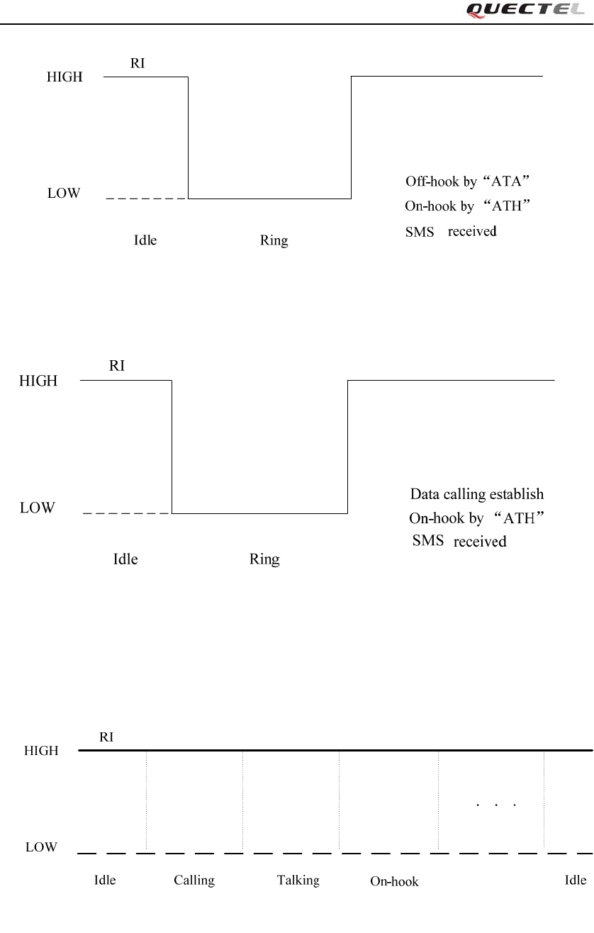
M10 Hardware Design
M10_HD_V3.0 - 59 -
Figure 38: RI behaviour of voice calling as a receiver
Figure 39: RI behaviour of data calling as a receiver
Figure 40: RI behaviour as a caller
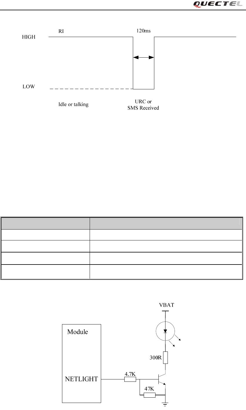
M10 Hardware Design
M10_HD_V3.0 - 60 -
Figure 41: RI behaviour of URC or SMS received
3.14. Network status indication
The NETLIGHT signal can be used to drive a network status indicator LED. The working state of
this pin is listed in Table 21.
Table 21: Working state of the NETLIGHT
State Module function
Off The module is not running.
64ms On/ 800ms Off The module is not synchronized with network.
64ms On/ 2000ms Off The module is synchronized with network.
64ms On/ 600ms Off GPRS data transfer is ongoing.
A reference circuit is shown in following figure.
Figure 42: Reference circuit of the NETLIGHT
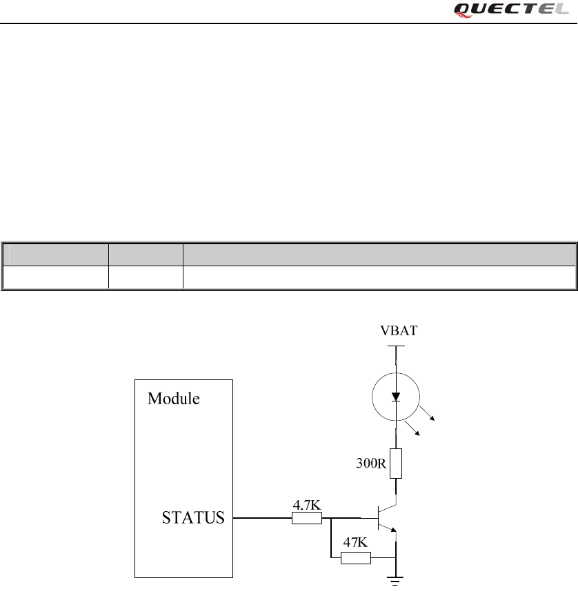
M10 Hardware Design
M10_HD_V3.0 - 61 -
3.15. Operating status indication
The STATUS pin is set as an output pin and can be used to judge whether module is power-on,
please refer to Chapter 3.4. In customer design, this pin can be connected to a GPIO of DTE or be
used to drive an LED in order to judge the module’s operation status. A reference circuit is shown
in figure 43.
Table 22: Pin definition of the STATUS
Figure 43: Reference circuit of the STATUS
3.16. General purpose input & output (GPIO)
The module provides a limited number of General Purpose Input/Output signal pins. The driving
capability of these pins is 4mA. Every GPIO can be configured as input or output, and set to high
or low when working as an output pin by “AT+CEQGPIO” command. Before using these GPIO
pins, customer should configure them with “AT+CEQGPIO=1,x,x,x,x” first. For details, please
refer to document [1].
Name Pin Function
STATUS 54 Indicate module’s operating status
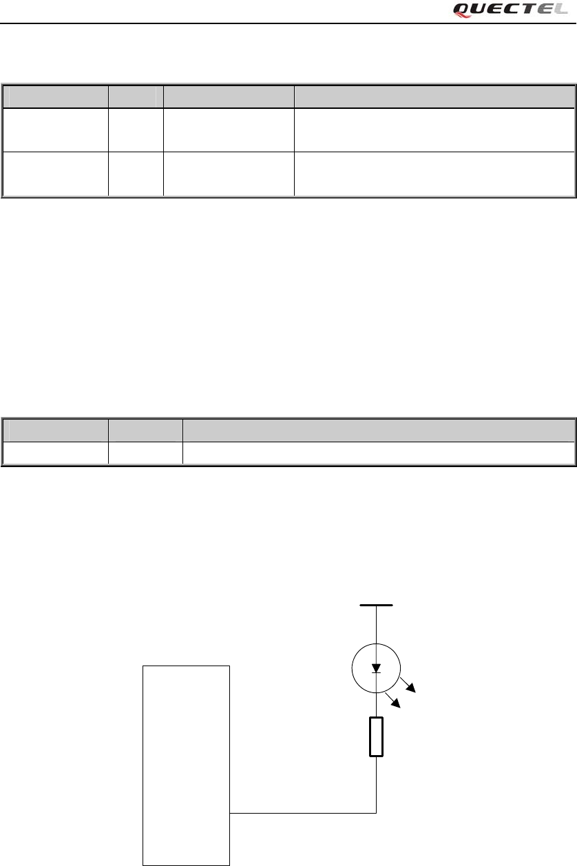
M10 Hardware Design
M10_HD_V3.0 - 62 -
Table 23: Pin definition of the GPIO interface
3.17. Open drain output (LIGHT_MOS)
The module provides an open drain output pin to control keyboard backlight. The output
LIGHT_MOS can sink 60mA. This open-drain output switch is high impedance when disabled.
Table 24: Pin definition of the LIGHT_MOS
Note: This function is not supported in the default firmware. There must be special firmware if
customer needs this function. Please contact Quectel for more details.
Module
300R
VBAT
LIGHT_MOS
Figure 44: Reference circuit of the LIGHT_MOS
Name Pin PU/PD Function
GPIO0 64 Pulled up internally
to 75K resistor
General Purpose Input/Output Port
GPIO1_KBC5 38 Pulled up internally
to 75K resistor
General Purpose Input/Output Port
Keypad interface KBC5
Name Pin Function
LIGHT_MOS 27 Open drain output port
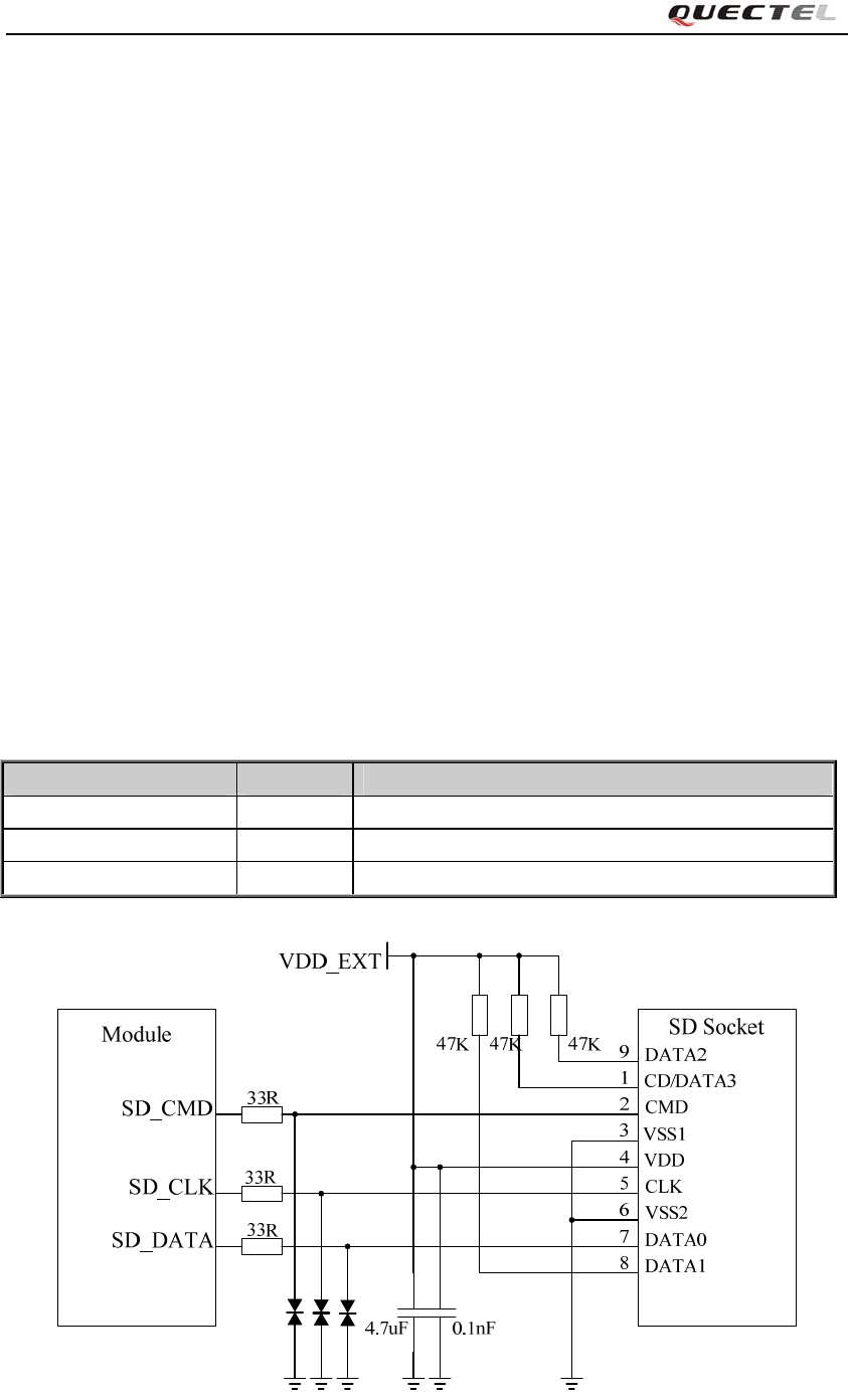
M10 Hardware Design
M10_HD_V3.0 - 63 -
3.18. SD card interface
The module provides SD card interface that supports many types of memory, such as Memory
Stick, SD/MCC card and T-Flash or Micro SD card. The following are the main features of SD
card interface.
Only supports 1bit serial mode
Dose not support the SPI mode SD/MMC memory card
Dose not support multiple SD memory cards
Dose not support hot plug
The data rate up to 26MHz in serial mode
Up to 32GB maximum memory card capacity
With the SD card interface features and reference circuit shown in figure 45, the users can easily
design the SD card application circuit to enhance the memory capacity of the module. The users
can store some high-capacity files to external memory card. Such as in the automotive application
system, the module can record and store the audio file to the SD card, and also can play the audio
files in SD card.
Table 25: Pin definition of the SD card interface
Figure 45: Reference circuit of SD card
Name Pin Function
SD_DATA 1 Data output and input signal of SD card
SD_CLK 2 Clock signal of SD card output
SD_CMD 3 Command signal of SD card output
M10 Hardware Design
M10_HD_V3.0 - 64 -
Table 26: Pin name of the SD card and T-Flash(Micro SD) card
In SD card interface designing, in order to ensure good communication performance with SD card,
it should be complied with following design principles.
Route SD card signals as short as possible. Ensure the length of trace do not exceed 20mm.
In order to offer good ESD protection, it is recommended to add TVS on signals with the
capacitance is less than 15pF.
Reserve external pull-up resistor for other data lines except the DATA0.
The SD_CLK and SD_DATA line must be shielded by GND in order to avoid interference.
The SD_CLK and SD_DATA and SD_CMD trace should be routed together and keep each
trace as close as possible.
Pin NO. Pin name of SD card Pin name of T-Flash(Micro SD) card
1 CD/DATA3 DATA2
2 CMD CD/DATA3
3 VSS1 CMD
4 VCC VCC
5 CLK CLK
6 VSS2 VSS
7 DATA0 DATA0
8 DATA1 DATA1
9 DATA2
M10 Hardware Design
M10_HD_V3.0 - 65 -
4. Antenna interface
The Pin 43 is the RF antenna pad. The RF interface has an impedance of 50Ω. A reference circuit
is shown in following figure. By default, the resistor R1 is 0 ohm and capacitor C1 and C2 are not
mounted.
MODULE
RF_ANT
R1 0R
C1
NM
C2
NM
Figure 46: Reference circuit of RF interface
4.1. Antenna installation
M10 provides an RF antenna PAD for customer’s antenna connection. The RF trace in host PCB
connecting to the module RF antenna pad should be micro-strip line or other types of RF trace,
whose characteristic resistance should be close to 50Ω. M10 comes with two grounding pads
which are next to the antenna pad in order to give a better grounding.
Table 27: Pin definition of the RF_ANT
To minimize the loss on the RF trace and RF cable, they should be designed carefully. It is
recommended that the insertion loss should try to meet the following requirements:
GSM850/EGSM900<1dB
DCS1800/PCS1900<1.5dB
Name Pin Function
RF_ANT 43 RF antenna pad
GND 42 Ground
GND 44 Ground
M10 Hardware Design
M10_HD_V3.0 - 66 -
4.2. RF output power
Table 28: The module conducted RF output power
Frequency Max Min
GSM850 33dBm ±2dB 5dBm±5dB
EGSM900 33dBm ±2dB 5dBm±5dB
DCS1800 30dBm ±2dB 0dBm±5dB
PCS1900 30dBm ±2dB 0dBm±5dB
Note: In GPRS 4 slots TX mode, the max output power is reduced by 2.5dB. This design
conforms to the GSM specification as described in chapter 13.16 of 3GPP TS 51.010-1.
4.3. RF receiving sensitivity
Table 29: The module conducted RF receiving sensitivity
Frequency Receive sensitivity
GSM850 < -108.5dBm
EGSM900 < -108.5dBm
DCS1800 < -108dBm
PCS1900 < -108dBm
4.4. Operating frequencies
Table 30: The module operating frequencies
Frequency Receive Transmit ARFCH
GSM850 869~894MHz 824~849MHz 128~251
EGSM900 925~960MHz 880~915MHz 0~124, 975~1023
DCS1800 1805~1880MHz 1710~1785MHz 512~885
PCS1900 1930~1990MHz 1850~1910MHz 512~810
4.5. Recommendation of RF pad welding
If external antenna is connected with RF cable welded on the RF pads, please refer to figure 47.
Any incorrect welding type may cause poor performance both in transmitting power and receiving
sensitivity.
M10 Hardware Design
M10_HD_V3.0 - 67 -
Figure 47: Recommendation of RF pad welding
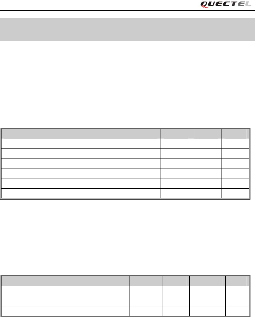
M10 Hardware Design
M10_HD_V3.0 - 68 -
5. Electrical, reliability and radio characteristics
5.1. Absolute maximum ratings
Absolute maximum ratings for power supply and voltage on digital and analog pins of module are
listed in the following table:
Table 31: Absolute maximum ratings
Parameter Min Max Unit
VBAT -0.3 4.7 V
Peak current of power supply 0 2 A
RMS current of power supply (during one TDMA- frame) 0 0.7 A
Voltage at digital pins -0.3 3.3 V
Voltage at analog pins -0.3 3.0 V
Voltage at digital/analog pins in POWER DOWN mode -0.25 0.25 V
5.2. Operating temperature
The operating temperature is listed in the following table:
Table 32: Operating temperature
Parameter Min Typ Max Unit
Normal temperature -35 25 +80 ℃
Restricted operation* -45 to -35 +80 to +85 ℃
Storage temperature -45 +90 ℃
* When the module works in this temperature range, the deviation from the GSM specification
may occur. For example, the frequency error or the phase error could increase.
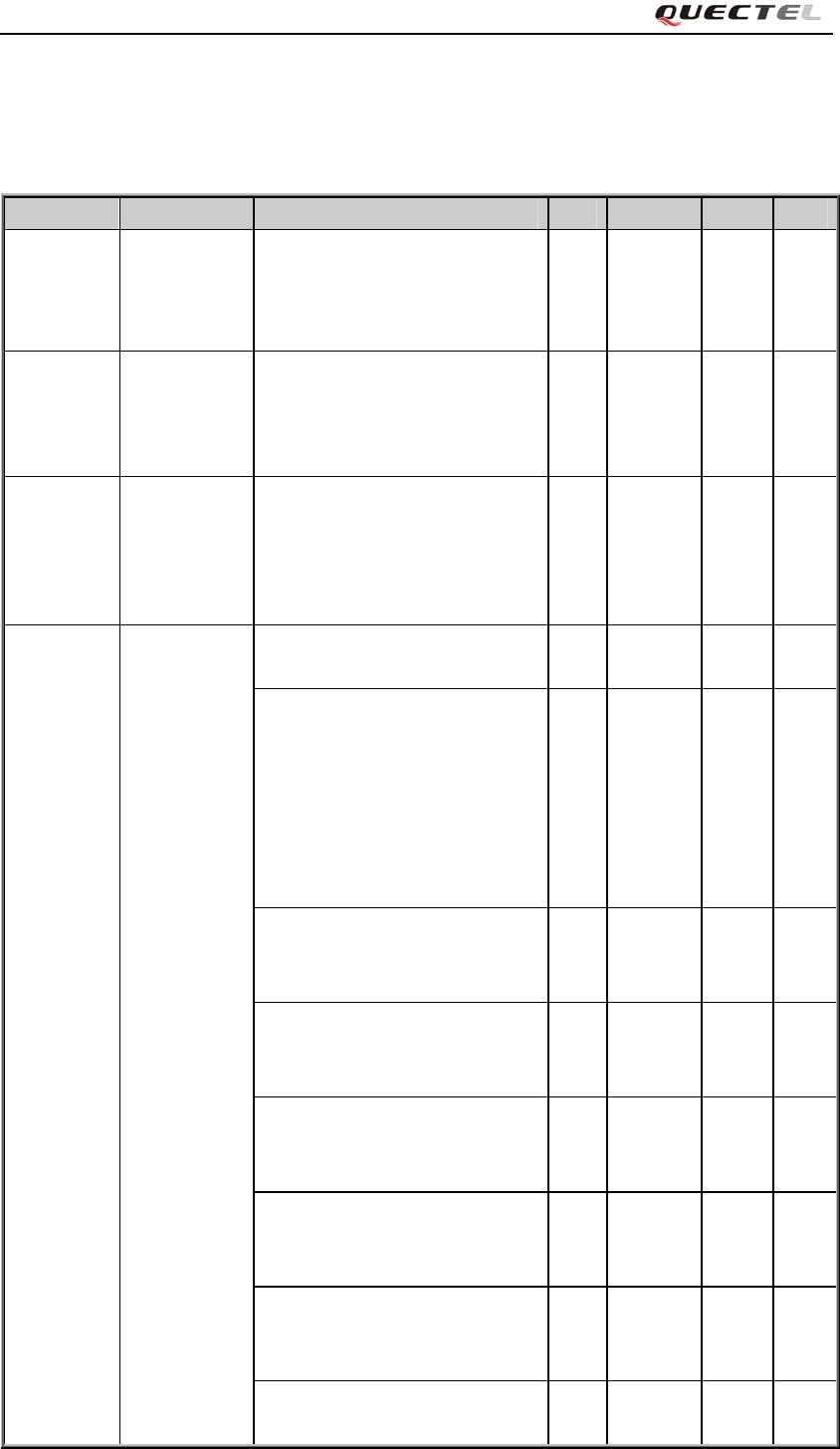
M10 Hardware Design
M10_HD_V3.0 - 69 -
5.3. Power supply ratings
Table 33: The module power supply ratings
Parameter Description Conditions Min Type Max Unit
VBAT Supply
voltage
Voltage must stay within the
min/max values, including
voltage drop, ripple, and spikes.
3.3 4.0 4.6 V
Voltage drop
during
transmitting
burst
Maximum power control level
on GSM850 and GSM900.
400 mV
Voltage
ripple
Maximum power control level
on GSM850 and GSM900
@ f<200kHz
@ f>200kHz
50
2
mV
mV
IVBAT
Average
supply
current
POWER DOWN mode
SLEEP mode @ DRX=5
29
1.1
uA
mA
Minimum functionality mode
AT+CFUN=0
IDLE mode
SLEEP mode
AT+CFUN=4
IDLE mode
SLEEP mode
13
0.84
13
0.83
mA
mA
mA
mA
IDLE mode
GSM850/EGSM900
DCS1800/PCS1900
13
13
mA
mA
TALK mode
GSM850/EGSM9001)
DCS1800/PCS19002)
209/208
191/202
mA
mA
DATA mode, GPRS (3 Rx,2Tx)
GSM850/EGSM9001)
DCS1800/PCS19002)
341/347
318/335
mA
mA
DATA mode, GPRS(2 Rx,3Tx)
GSM850/EGSM9001)
DCS1800/PCS19002)
394/408
377/396
mA
mA
DATA mode, GPRS (4 Rx,1Tx)
GSM850/EGSM9001)
DCS1800/PCS19002)
225/226
210/219
mA
mA
DATA mode, GPRS(1Rx,4Tx)
GSM850/EGSM9001)
449/464
mA
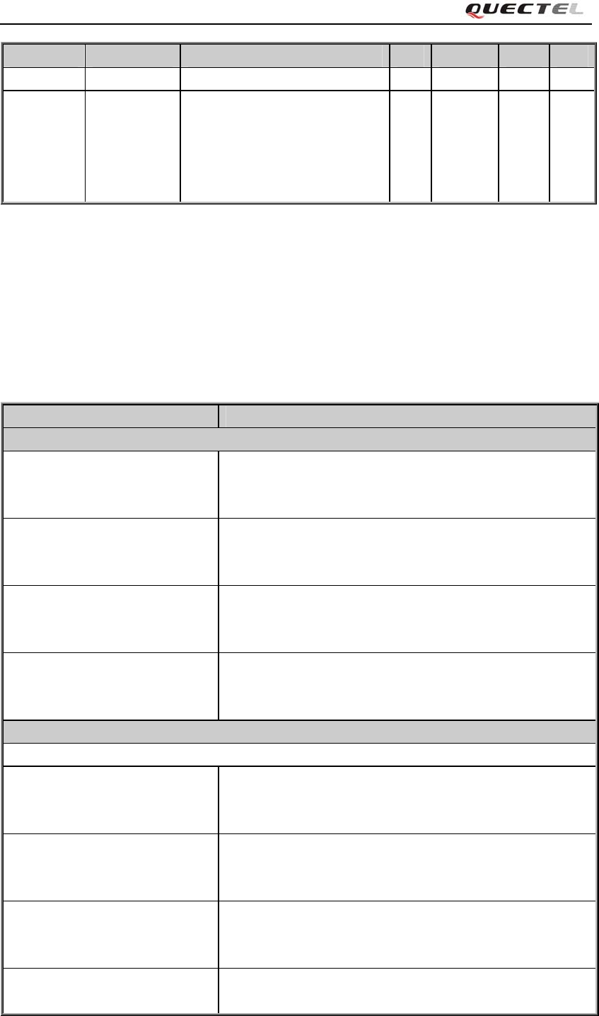
M10 Hardware Design
M10_HD_V3.0 - 70 -
Parameter Description Conditions Min Type Max Unit
DCS1800/PCS19002) 423/445 mA
Peak supply
current
(during
transmission
slot)
Maximum power control level
on GSM900.
1.6 1.8 A
1) Power control level PCL 5
2) Power control level PCL 0
5.4. Current consumption
The values of current consumption are shown in Table 34.
Table 34: The module current consumption
Condition Current Consumption
Voice Call
GSM850 @power level #5 <300mA,Typical 209mA
@power level #12,Typical 96mA
@power level #19,Typical 73mA
GSM900 @power level #5 <300mA,Typical 208mA
@power level #12,Typical 96mA
@power level #19,Typical 73mA
DCS1800 @power level #0 <250mA,Typical 191mA
@power level #7,Typical 93mA
@power level #15,Typical 70mA
PCS1900 @power level #0 <250mA,Typical 202mA
@power level #7,Typical 95mA
@power level #15,Typical 71mA
GPRS Data
DATA mode, GPRS ( 1 Rx,1 Tx ) CLASS 12
GSM850 @power level #5 <350mA,Typical 199mA
@power level #12,Typical 87mA
@power level #19,Typical 63mA
EGSM 900 @power level #5 <350mA,Typical 200mA
@power level #12,Typical 96mA
@power level #19,Typical 70mA
DCS 1800 @power level #0 <300mA,Typical 184mA
@power level #7,Typical 82mA
@power level #15,Typical 66mA
PCS 1900 @power level #0 <300mA,Typical 192mA
@power level #7,Typical 82mA

M10 Hardware Design
M10_HD_V3.0 - 71 -
@power level #15,Typical 66mA
DATA mode, GPRS ( 3 Rx, 2 Tx ) CLASS 12
GSM850 @power level #5 <550mA,Typical 341mA
@power level #12,Typical 135mA
@power level #19,Typical 85mA
EGSM 900 @power level #5 <550mA,Typical 347mA
@power level #12,Typical 156mA
@power level #19,Typical 103mA
DCS 1800 @power level #0 <450mA,Typical 318mA
@power level #7,Typical 118mA
@power level #15,Typical 84mA
PCS 1900 @power level #0 <450mA,Typical 335mA
@power level #7,Typical 128mA
@power level #15,Typical 95mA
DATA mode, GPRS ( 2 Rx, 3 Tx ) CLASS 12
GSM850 @power level #5 <600mA,Typical 394mA
@power level #12,Typical 176mA
@power level #19,Typical 102mA
EGSM 900 @power level #5 <600mA,Typical 408mA
@power level #12,Typical 189mA
@power level #19,Typical 110mA
DCS 1800 @power level #0 <490mA,Typical 377mA
@power level #7,Typical 147mA
@power level #15,Typical 97mA
PCS 1900 @power level #0 <480mA,Typical 396mA
@power level #7,Typical 146mA
@power level #15,Typical 98mA
DATA mode, GPRS ( 4 Rx,1 Tx ) CLASS 12
GSM850 @power level #5 <350mA,Typical 225mA
@power level #12,Typical 87mA
@power level #19,Typical 62mA
EGSM 900 @power level #5 <350mA,Typical 226mA
@power level #12,Typical 97mA
@power level #19,Typical 69mA
DCS 1800 @power level #0 <300mA,Typical 210mA
@power level #7,Typical 82mA
@power level #15,Typical 66mA
PCS 1900 @power level #0 <300mA,Typical 219mA
@power level #7,Typical 82mA
@power level #15,Typical 66mA
DATA mode, GPRS ( 1 Rx, 4 Tx ) CLASS 12
GSM850 @power level #5 <660mA,Typical 449mA
@power level #12,Typical 207mA
M10 Hardware Design
M10_HD_V3.0 - 72 -
@power level #19,Typical 109mA
EGSM 900 @power level #5 <660mA,Typical 464mA
@power level #12,Typical 221mA
@power level #19,Typical 117mA
DCS 1800 @power level #0 <530mA,Typical 423mA
@power level #7,Typical 166mA
@power level #15,Typical 99mA
PCS 1900 @power level #0 <530mA,Typical 445mA
@power level #7,Typical 165mA
@power level #15,Typical 100mA
Note: GPRS Class 12 is the default setting. The module can be configured from GPRS Class 1
to Class 12 by “AT+QGPCLASS”. Setting to lower GPRS class would make it easier to design
the power supply for the module.
5.5. Electro-static discharge
Although the GSM engine is generally protected against Electrostatic Discharge (ESD),
precautions about ESD protection should still be emphasized. Proper ESD handling and packaging
procedures must be applied throughout the processing, handling and operation of any applications
using the module.
The measured ESD values of module are shown as the following table:
Table 35: The ESD endurance (Temperature:25℃,Humidity:45 %)
Tested point Contact discharge Air discharge
VBAT,GND ±5KV ±12KV
PWRKEY ±4KV +8KV/-6 KV
SIM Card Interface ±4KV +8KV/-6 KV
Antenna port ±5KV ±10KV
SPK1P/1N, SPK2P/2N,
MIC1P/1N, MIC2P/2N ±4KV +8KV/-6 KV
M10
M10
_
6.
M
Thi
s
6.1.
Hardware D
e
_
HD_V3.0
M
echani
s
chapter des
c
.
Mechanic
e
sign
cal dim
e
c
ribes the me
al dimensi
o
Figure
4
e
nsions
c
hanical dim
o
ns of mo
d
4
8: M10 top
a
m
ensions of t
h
d
ule
a
nd side di
m
e module.
m
ensions(U
n
n
it: mm)
- 73 -
M10 Hardware Design
M10_HD_V3.0 - 74 -
test point
Figure 49: M10 bottom dimensions(Unit: mm)
Figure 50: PAD bottom dimensions(Unit: mm)
M10 Hardware Design
M10_HD_V3.0 - 75 -
6.2. Footprint of recommendation
single pad
M10 Hardware Design
M10_HD_V3.0 - 76 -
keepout area
module dimension
safe area line
Figure 51: Footprint of recommendation(Unit: mm)
Note1
:
Keep out the area below the test point in the host PCB. Place solder mask.
Note2
:
In order to maintain the module, keep about 3mm between the module and other
components in host PCB.
Note3
:
Keep out area in above figure in which is forbid to pour GND copper. Since the RF test
point in this area, avoid generating parasitic capacitance between RF test point and
GND.
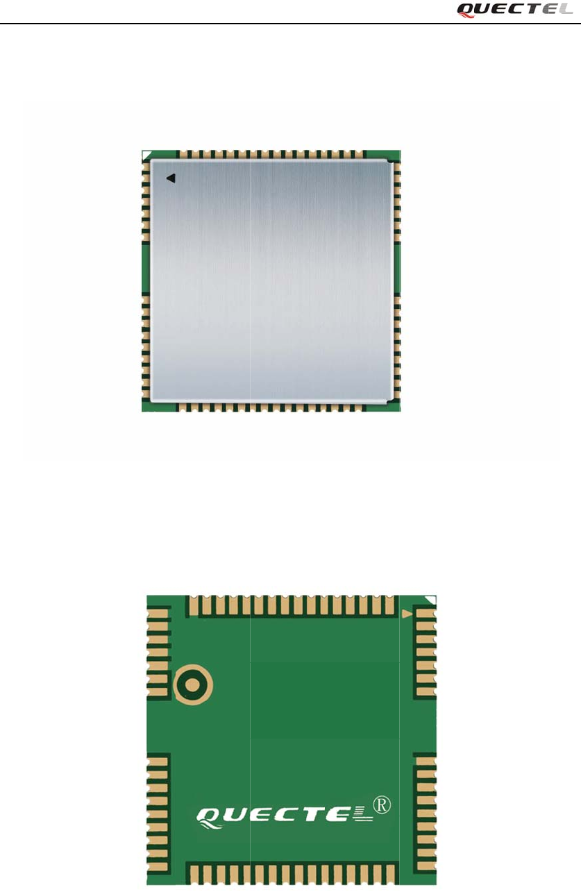
M10
M10
_
6.3.
6.4.
Hardware D
e
_
HD_V3.0
.
Top view
.
Bottom vi
e
sign
of the mo
d
ew of the
m
F
d
ule
Figure 52:
m
odule
F
igure 53: B
Top view o
f
B
ottom view
o
f
the module
o
f the modu
l
l
e
- 77 -
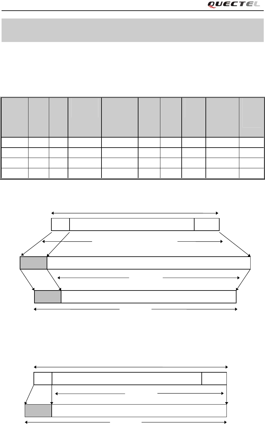
M10 Hardware Design
M10_HD_V3.0 - 78 -
Appendix A: GPRS coding schemes
Four coding schemes are used in GPRS protocol. The differences between them are shown in
Table 36.
Table 36: Description of different coding schemes
Scheme Code
rate
USF Pre-coded
USF
Radio
Block
excl.USF
and BCS
BCS Tail Coded
bits
Punctured
bits
Data
rate
Kb/s
CS-1 1/2 3 3 181 40 4 456 0 9.05
CS-2 2/3 3 6 268 16 4 588 132 13.4
CS-3 3/4 3 6 312 16 4 676 220 15.6
CS-4 1 3 12 428 16 - 456 - 21.4
Radio block structure of CS-1, CS-2 and CS-3 is shown as Figure 54:
Figure 54: Radio block structure of CS-1, CS-2 and CS-3
Radio block structure of CS-4 is shown as Figure 55:
Figure 55: Radio block structure of CS-4
Rate 1/2 convolutional coding
Puncturing
456 bits
USF BCS
Radio Bloc
k
Block
Code
N
o coding
456 bits
USF BCS
Radio Bloc
k
M10 Hardware Design
M10_HD_V3.0 - 79 -
Appendix B: GPRS multi-slot classes
Twenty-nine classes of GPRS multi-slot modes are defined for MS in GPRS specification.
Multi-slot classes are product dependant, and determine the maximum achievable data rates in
both the uplink and downlink directions. Written as 3+1 or 2+2, the first number indicates the
amount of downlink timeslots, while the second number indicates the amount of uplink timeslots.
The active slots determine the total number of slots the GPRS device can use simultaneously for
both uplink and downlink communications. The description of different multi-slot classes of the
M10 module support is shown in Table 37.
Table 37: GPRS multi-slot classes
Multislot class Downlink slots Uplink slots Active slots
1 1 1 2
2 2 1 3
3 2 2 3
4 3 1 4
5 2 2 4
6 3 2 4
7 3 3 4
8 4 1 5
9 3 2 5
10 4 2 5
11 4 3 5
12 4 4 5

Shanghai Quectel Wireless Solutions Co., Ltd.
Room 501, Building 13, No.99, Tianzhou Road, Shanghai, China 200233
Tel: +86 21 5108 6236
Mail: info@quectel.com