Quectel Wireless Solutions 201208M80 GSM/GPRS Module User Manual M10 Hardware Design
Quectel Wireless Solutions Company Limited GSM/GPRS Module M10 Hardware Design
UserManual.wiki
>
Quectel Wireless Solutions
>
201208M80 User Manual
User Manual
Navigation menu
Upload a User Manual
Namespaces
Wiki Guide
HTML
PDF
Info
Views
User Manual
Discussion / Help
Navigation
![M80 Hardware Design M80_HD_V1.2 - 10 - 1. Introduction This document defines the M80 module and describes the hardware interface of M80 which are connected with the customer application and the air interface. This document can help customers quickly understand module interface specifications, electrical and mechanical details. Associated with application notes and user guide, customers can use M80 module to design and set up mobile applications easily. 1.1. Related documents Table 1: Related documents SN Document name Remark [1] M80_ATC AT commands set [2] ITU-T Draft new recommendation V.25ter Serial asynchronous automatic dialing and control [3] GSM 07.07 Digital cellular telecommunications (Phase 2+); AT command set for GSM Mobile Equipment (ME) [4] GSM 07.10 Support GSM 07.10 multiplexing protocol [5] GSM 07.05 Digital cellular telecommunications (Phase 2+); Use of Data Terminal Equipment – Data Circuit terminating Equipment (DTE – DCE) interface for Short Message Service (SMS) and Cell Broadcast Service (CBS) [6] GSM 11.14 Digital cellular telecommunications (Phase 2+); Specification of the SIM Application Toolkit for the Subscriber Identity module – Mobile Equipment (SIM – ME) interface [7] GSM 11.11 Digital cellular telecommunications (Phase 2+); Specification of the Subscriber Identity module – Mobile Equipment (SIM – ME) interface [8] GSM 03.38 Digital cellular telecommunications (Phase 2+); Alphabets and language-specific information [9] GSM 11.10 Digital cellular telecommunications (Phase 2); Mobile Station (MS) conformance specification; Part 1: Conformance specification [10] GSM_UART_AN UART port application notes [11] GSM_FW_Upgrade_AN01 GSM Firmware upgrade application note [12] M80_EVB_UGD M80 EVB user guide [13] M80_Charging_AN M80 charging application notes](https://usermanual.wiki/Quectel-Wireless-Solutions/201208M80/User-Guide-1783735-Page-10.png)
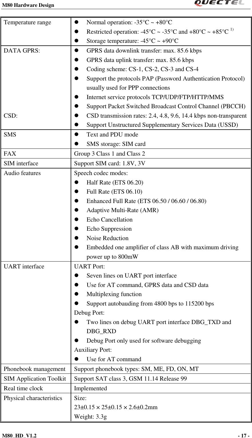
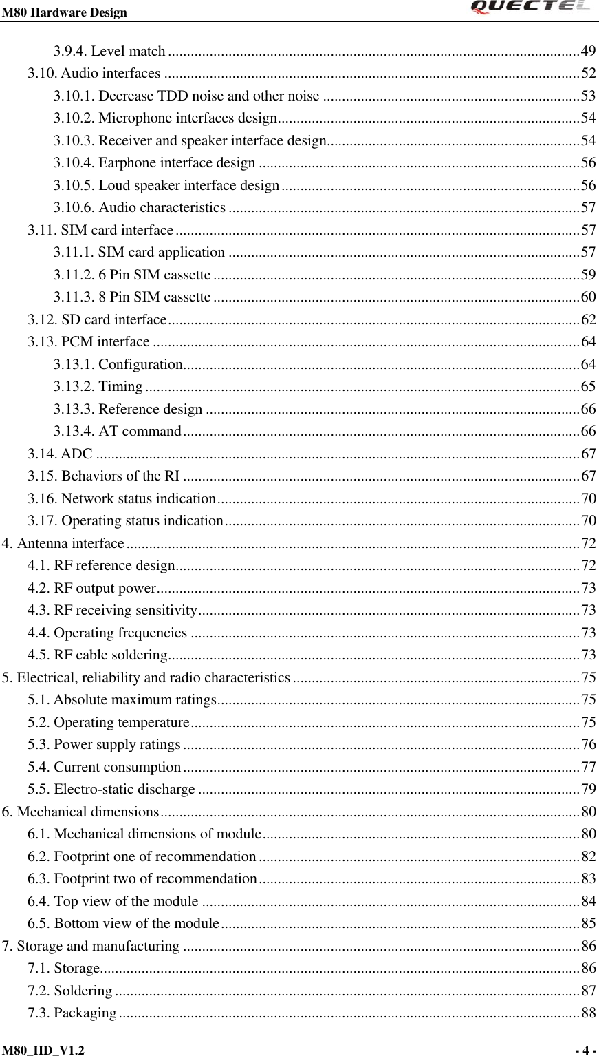
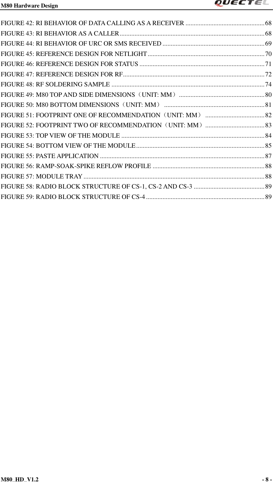
![M80 Hardware Design M80_HD_V1.2 - 19 - Serial FlashBaseband EnginePAMPMUPower supplyRTCChargeUARTSIMSDEINTTurn on/offIndicatorADCPCMTransceiverSaw26MHz 32kHzAudiocodecRF Figure 1: Module functional diagram 2.3. Evaluation board In order to help customer to develop applications with M80, Quectel supplies an evaluation board (EVB), RS-232 to USB cable, power adapter, earphone, antenna and other peripherals to control or test the module. For details, please refer to the document [12].](https://usermanual.wiki/Quectel-Wireless-Solutions/201208M80/User-Guide-1783735-Page-19.png)
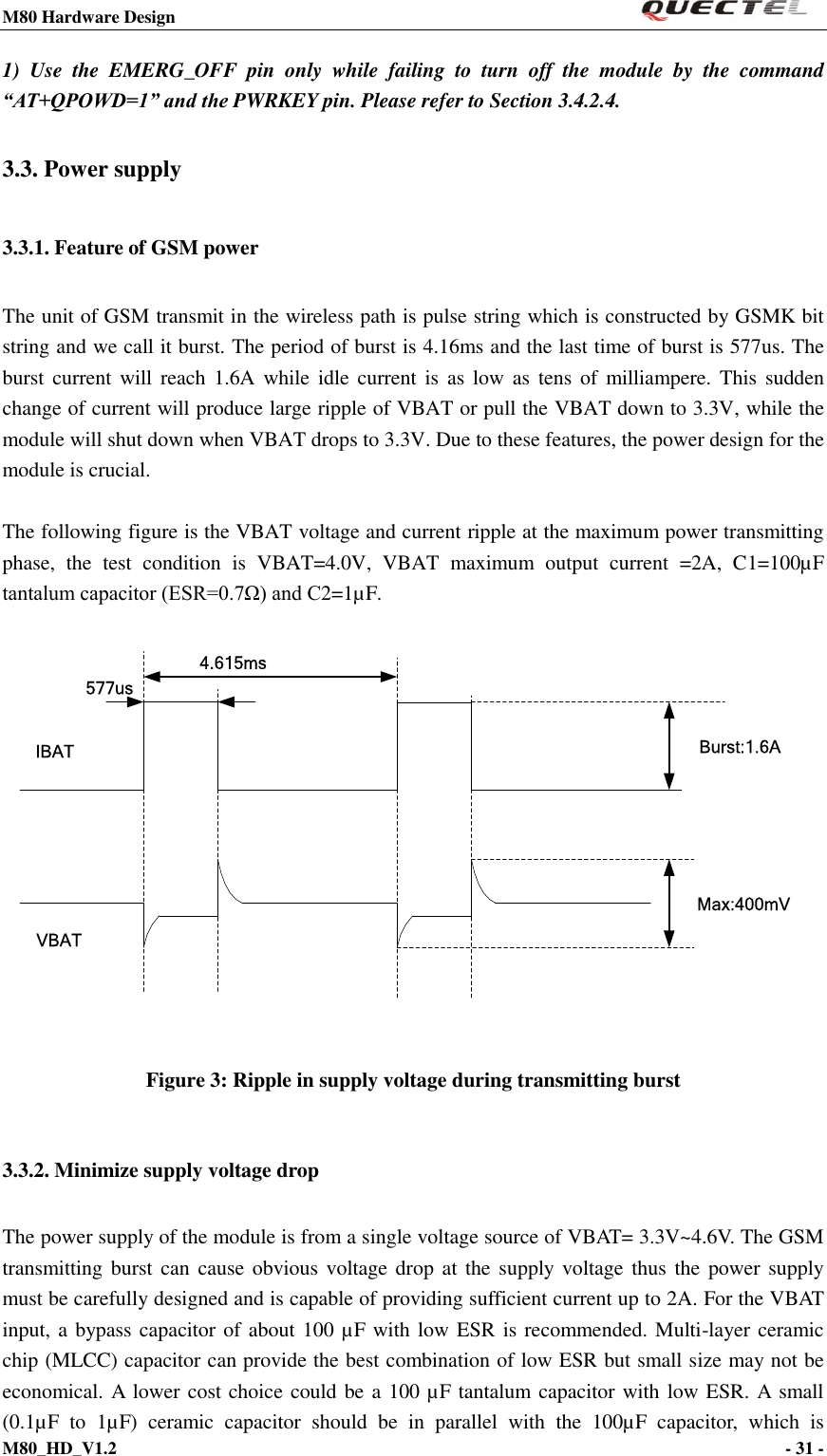
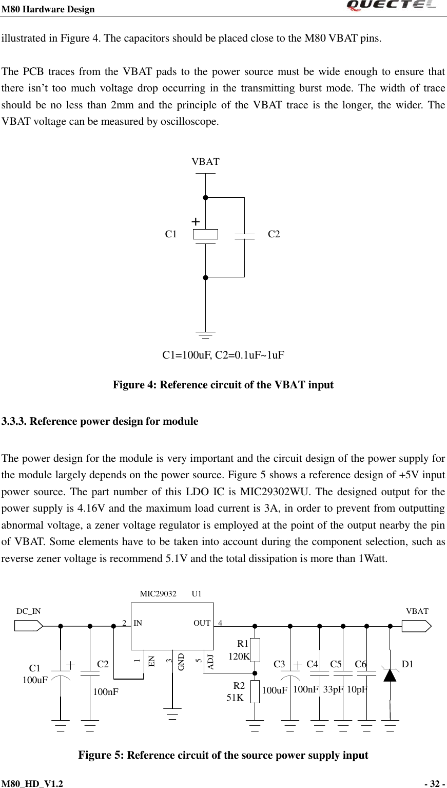
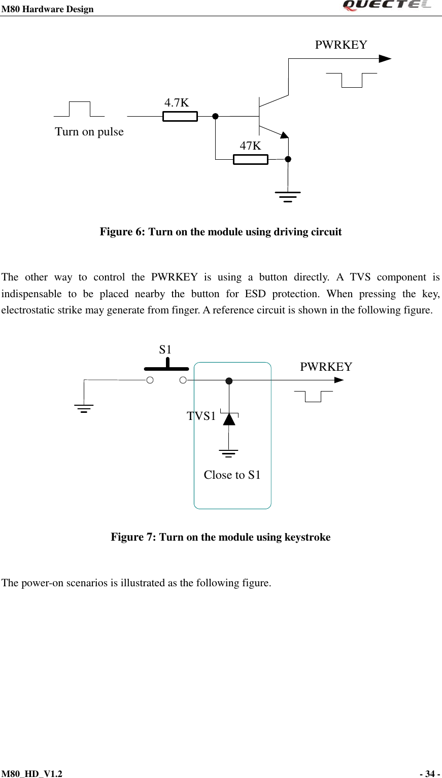
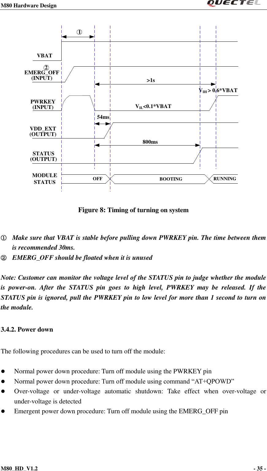
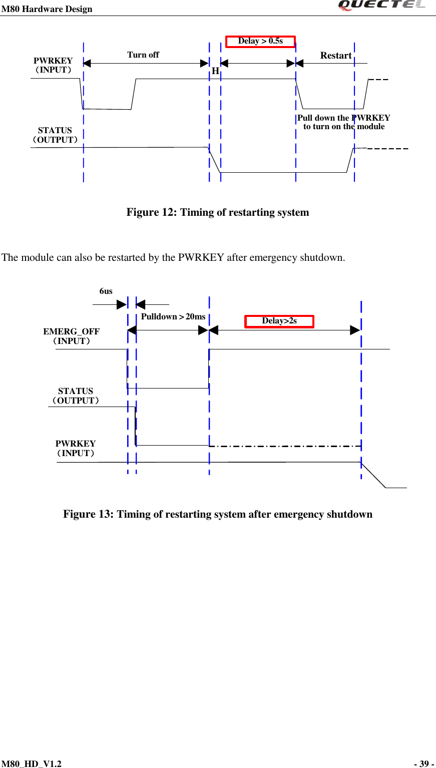
![M80 Hardware Design M80_HD_V1.2 - 33 - 3.3.4. Monitor power supply To monitor the supply voltage, you can use the “AT+CBC” command which includes three parameters: charging status, remaining battery capacity and voltage value (in mV). It returns the 0-100 percent of battery capacity and actual value measured between VBAT and GND. The voltage is automatically measured in period of 5s. The displayed voltage (in mV) is averaged over the last measuring period before the “AT+CBC” command is executed. For details, please refer to document [1]. 3.4. Power on and down scenarios 3.4.1. Power on The module can be turned on by PWRKEY pin. The module is set to autobauding mode (AT+IPR=0) in default configuration. In the autobauding mode, the URC “RDY” after powering on is not sent to host controller. When the module receives AT command, it will be powered on after a delay of 2 or 3 seconds. Host controller should firstly send an “AT” or “at” string in order that the module can detect baud rate of host controller, and it should send the second or the third “AT” or “at” string until receiving “OK” string from the module. Then an “AT+IPR=x;&W” should be sent to set a fixed baud rate for the module and save the configuration to flash memory of the module. After these configurations, the URC “RDY” would be received from the UART Port of the module every time when the module is powered on. Refer to section “AT+IPR” in document [1]. The hardware flow control is disabled in default configuration. In the simple UART port which means that only TXD, RXD, GND of the module is connected to host. CTS and RTS are pulled down internally by software. In this condition, the module can transmit and receive data freely. On the other side, if RTS, CTS connect to the host together with TXD, RXD, GND, whether or not to transmit and receive data depends on the level of RTS and CTS. Then whenever hardware flow is present or not, the URC “RDY” is sent to host controller in the fixed band rate. 3.4.1.1. Power on module using the PWRKEY pin Customer’s application can turn on the module by driving the pin PWRKEY to a low level voltage and after STATUS pin outputs a high level, PWRKEY pin can be released. Customer may monitor the level of the STATUS pin to judge whether the module is power-on or not. An open collector driver circuit is suggested to control the PWRKEY. A simple reference circuit is illustrated as below.](https://usermanual.wiki/Quectel-Wireless-Solutions/201208M80/User-Guide-1783735-Page-33.png)
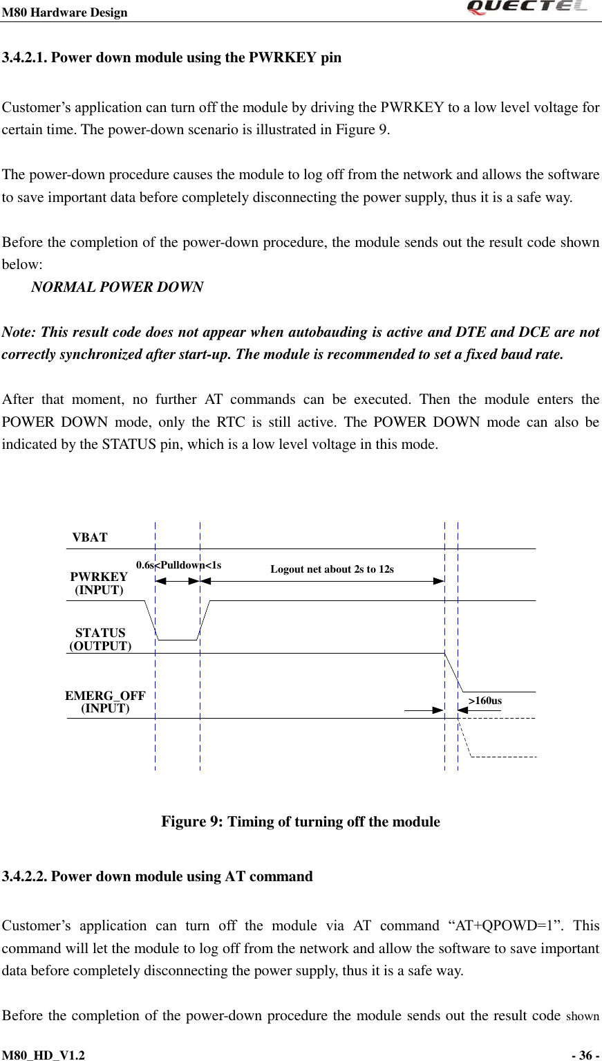
![M80 Hardware Design M80_HD_V1.2 - 37 - below: NORMAL POWER DOWN After that moment, no further AT commands can be executed. And then the module enters the POWER DOWN mode, only the RTC is still active. The POWER DOWN mode can also be indicated by STATUS pin, which is a low level voltage in this mode. Please refer to document [1] for details about the AT command “AT+QPOWD”. 3.4.2.3. Over-voltage or under-voltage automatic shutdown The module will constantly monitor the voltage applied on the VBAT, if the voltage is ≤ 3.5V, the following URC will be presented: UNDER_VOLTAGE WARNING If the voltage is ≥ 4.5V, the following URC will be presented: OVER_VOLTAGE WARNING The uncritical voltage range is 3.3V to 4.6V. If the voltage is > 4.6V or <3.3V, the module would automatically shutdown itself. If the voltage is <3.3V, the following URC will be presented: UNDER_VOLTAGE POWER DOWN If the voltage is >4.6V, the following URC will be presented: OVER_VOLTAGE POWER DOWN Note: These result codes don’t appear when autobauding is active and DTE and DCE are not correctly synchronized after start-up. The module is recommended to set to a fixed baud rate. After that moment, no further AT commands can be executed. The module logs off from network and enters POWER DOWN mode, and only RTC is still active. The POWER DOWN mode can also be indicated by the pin STATUS, which is a low level voltage in this mode. 3.4.2.4. Emergency shutdown using EMERG_OFF pin The module can be shut down by driving the pin EMERG_OFF to a low level voltage over 20ms and then releasing it. The EMERG_OFF line can be driven by an open-drain /collector driver or a button. The circuit is illustrated as the following figures.](https://usermanual.wiki/Quectel-Wireless-Solutions/201208M80/User-Guide-1783735-Page-37.png)
![M80 Hardware Design M80_HD_V1.2 - 40 - 3.5. Charging interface M80 provides charging function for rechargeable Li-Ion or Lithium Polymer battery. It is introduced simply in this document. If you want to get more information about charging, please refer to document [13]. Table 8: Pin definition of the charging Item No. I/O Description. GATDRV 74 O Charge driving CHGLDO 73 I Charge power CHGDET 72 I Charging detect ISENSE 71 I Current sense BATSNS 70 I VBAT voltage sense 3.6. Power saving Upon system requirement, there are several actions to drive the module to enter low current consumption status. For example, “AT+CFUN” can be used to set module into minimum functionality mode and DTR hardware interface signal can be used to lead system to SLEEP mode. 3.6.1. Minimum functionality mode Minimum functionality mode reduces the functionality of the module to a minimum level, thus minimize the current consumption when the slow clocking mode is activated at the same time. This mode is set with the “AT+CFUN” command which provides the choice of the functionality levels <fun>=0,1,4. 0: minimum functionality 1: full functionality (default) 4: disable both transmitting and receiving of RF part If the module is set to minimum functionality by “AT+CFUN=0”, the RF function and SIM card function would be disabled. In this case, the UART port is still accessible, but all AT commands correlative with RF function or SIM card function will not be accessible. If the module has been set by “AT+CFUN=4”, the RF function will be disabled, the UART port is still active. In this case, all AT commands correlative with RF function will be not accessible. After the module is set by “AT+CFUN=0” or “AT+CFUN=4”, it can return to full functionality by](https://usermanual.wiki/Quectel-Wireless-Solutions/201208M80/User-Guide-1783735-Page-40.png)
![M80 Hardware Design M80_HD_V1.2 - 41 - “AT+CFUN=1”. For detailed information about “AT+CFUN”, please refer to document [1]. 3.6.2. SLEEP mode The SLEEP mode is disabled in default software configuration. Customer’s application can enable this mode by “AT+QSCLK=1”. On the other hand, the default setting is “AT+QSCLK=0” and in this mode, the module can’t enter SLEEP mode. When “AT+QSCLK=1” is sent to the module, customer’s application can control the module to enter or exit from the SLEEP mode through pin DTR. When DTR is set to high level, and there is no on-air or hardware interrupt such as GPIO interrupt or data on UART port, the module will enter SLEEP mode automatically. In this mode, the module can still receive voice, SMS or GPRS paging from network but the UART port is not accessible. 3.6.3. Wake up module from SLEEP mode When the module is in the SLEEP mode, the following methods can wake up the module. If the DTR Pin is set low, it would wake up the module from the SLEEP mode. The UART port will be active within 20ms after DTR is changed to low level. Receive a voice or data call from network wakes up module. Receiving an SMS from network wakes up module. Note: DTR pin should be held low level during communication between the module and DTE. 3.7. Summary of state transitions Table 9: Summary of state transition Current mode Next mode Power down Normal mode Sleep mode Power down Use PWRKEY Normal mode AT+QPOWD, use PWRKEY pin, or use EMERG_OFF pin Use AT command “AT+QSCLK=1” and pull DTR up Sleep mode Use PWRKEY pin, or use EMERG_OFF pin Pull DTR down or incoming call or SMS or GPRS](https://usermanual.wiki/Quectel-Wireless-Solutions/201208M80/User-Guide-1783735-Page-41.png)
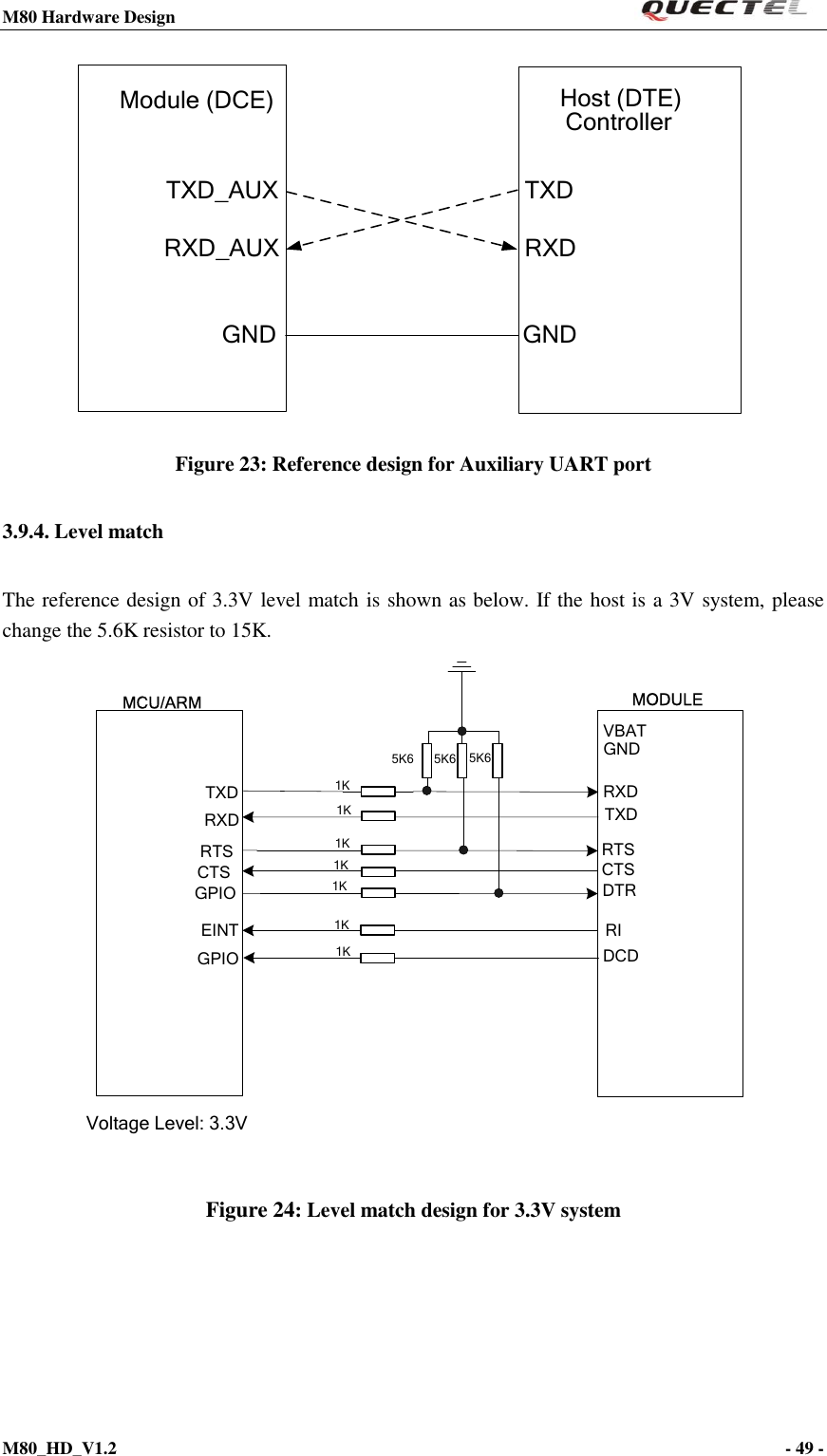
![M80 Hardware Design M80_HD_V1.2 - 43 - Figure 17: Seiko XH414H-IV01E Charge Characteristics 3.9. Serial interfaces The module provides three serial ports: UART Port, Debug Port and Auxiliary UART Port. The module is designed as a DCE (Data Communication Equipment), following the traditional DCE-DTE (Data Terminal Equipment) connection. Autobauding function supports baud rate from 4800bps to 115200bps. The UART Port: TXD: Send data to RXD of DTE. RXD: Receive data from TXD of DTE. RTS: Requests to send. CTS: Clear to send. DTR: DTE is ready and inform DCE (this pin can wake the module up). RI: Ring indicator (when the call, SMS, data of the module are coming, the module will output signal to inform DTE). DCD: Data carrier detection (the validity of this pin demonstrates the communication link is set up). Note: The module disables hardware flow control by default. When hardware flow control is required, RTS and CTS should be connected to the host. AT command “AT+IFC=2,2” is used to enable hardware flow control. AT command “AT+IFC=0,0” is used to disable the hardware flow control. For more details, please refer to document [1].](https://usermanual.wiki/Quectel-Wireless-Solutions/201208M80/User-Guide-1783735-Page-43.png)
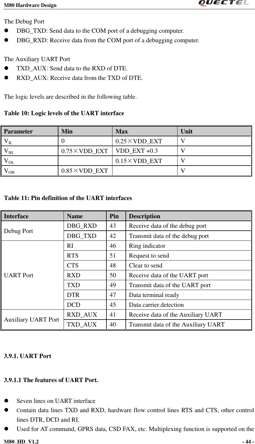
![M80 Hardware Design M80_HD_V1.2 - 45 - UART Port. So far only the basic mode of multiplexing is available. Support the communication baud rates as the following: 300,600,1200,2400,4800,9600,14400,19200,28800,38400,57600,115200. The default setting is autobauding mode. Support the following baud rates for Autobauding function: 4800, 9600, 19200, 38400, 57600, 115200. The module disables hardware flow control by default. AT command “AT+IFC=2,2” is used to enable hardware flow control. After setting a fixed baud rate or Autobauding, please send “AT” string at that rate. The UART port is ready when it responds “OK”. Autobauding allows the module to detect the baud rate by receiving the string “AT” or “at” from the host or PC automatically, which gives module flexibility without considering which baud rate is used by the host controller. Autobauding is enabled by default. To take advantage of the autobauding mode, special attention should be paid according to the following requirements: Synchronization between DTE and DCE: When DCE (the module) powers on with the autobauding enabled, it is recommended to wait 2 to 3 seconds before sending the first AT character. After receiving the “OK” response, DTE and DCE are correctly synchronized. If the host controller needs URC in the mode of autobauding, it must be synchronized firstly. Otherwise the URC will be discarded. Restrictions on autobauding operation: The UART port has to be operated at 8 data bits, no parity and 1 stop bit (factory setting). The “At” and “aT” commands can’t be used. Only the strings “AT” or “at” can be detected (neither “At” nor “aT”). The Unsolicited Result Codes like "RDY", "+CFUN: 1" and "+CPIN: READY” will not be indicated when the module is turned on with autobauding enabled and not be synchronized. Any other Unsolicited Result Codes will be sent at the previous baud rate before the module detects the new baud rate by receiving the first “AT” or “at” string. The DTE may receive unknown characters after switching to new baud rate. It is not recommended to switch to autobauding from a fixed baud rate. If autobauding is active it is not recommended to switch to multiplex mode. Note: To assure reliable communication and avoid any problems caused by undetermined baud rate between DCE and DTE, it is strongly recommended to configure a fixed baud rate and save it instead of using autobauding after start-up. For more details, please refer to Section “AT+IPR” in document [1].](https://usermanual.wiki/Quectel-Wireless-Solutions/201208M80/User-Guide-1783735-Page-45.png)
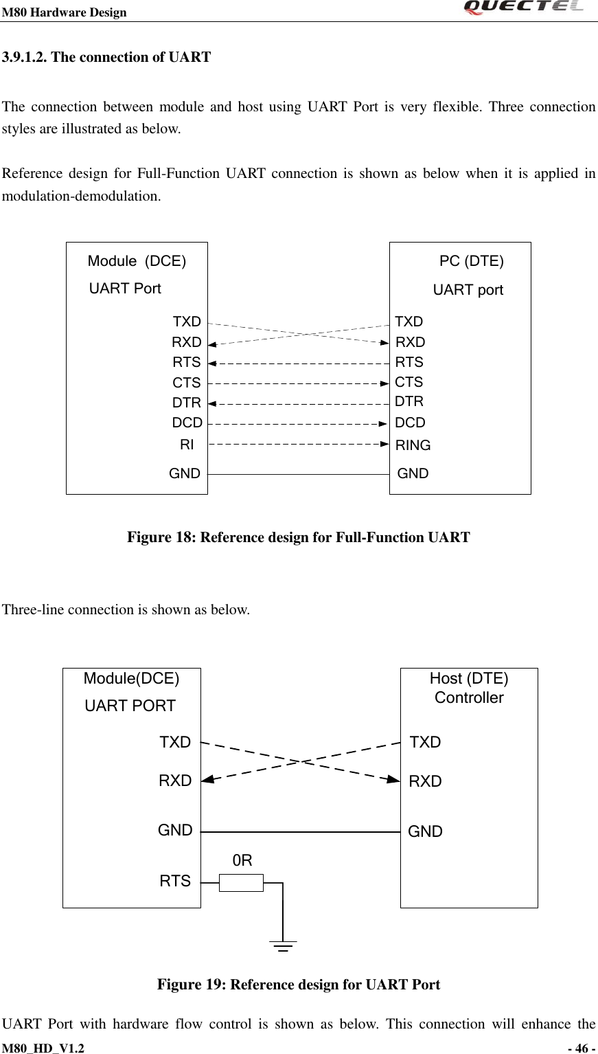
![M80 Hardware Design M80_HD_V1.2 - 47 - reliability of the mass data communication. Host (DTE) Controller Module(DCE)RTSCTSRTSCTSGNDRXDTXD TXDRXDGND Figure 20: Reference design for UART Port with hardware flow control 3.9.1.3. Software upgrade The TXD, RXD can be used to upgrade software. The PWRKEY pin must be pulled down before the software upgrade. Please refer to the following figures for software upgrade. IO Connector TXDRXDGNDPWRKEY Module (DCE) Serial portTXDRXDGNDPWRKEY Figure 21: Reference design software upgrade Note: The firmware of module might need to be upgraded due to certain reasons, it is recommended to reserve these pins in the host board for firmware upgrade. For detailed design, please refer to document [11].](https://usermanual.wiki/Quectel-Wireless-Solutions/201208M80/User-Guide-1783735-Page-47.png)
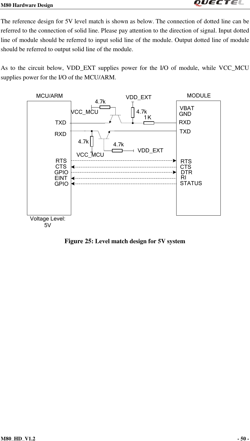
![M80 Hardware Design M80_HD_V1.2 - 48 - 3.9.2. Debug Port Debug Port Two lines: DBG_TXD and DBG_RXD It outputs log information automatically. Debug Port is only used for software debugging and its baud rate must be configured as 460800bps. Debug ComputerTXDRXDGND Module (DCE) Debug portDBG_TXDDBG_RXD GND Figure 22: Reference design for Debug Port 3.9.3. Auxiliary UART Port Auxiliary UART Port Two data lines: TXD_AUX and RXD_AUX Auxiliary UART port is used for AT command only and doesn’t support GPRS data, CSD FAX, Multiplexing function etc. Auxiliary UART port supports the communication baud rates as the following: 4800, 9600, 14400, 19200,28800,38400,57600,115200. The default baud rate setting is 115200bps, and doesn’t support autobauding. The baud rate can be modified by AT+QSEDCB command. For more details, please refer to document [1].](https://usermanual.wiki/Quectel-Wireless-Solutions/201208M80/User-Guide-1783735-Page-48.png)
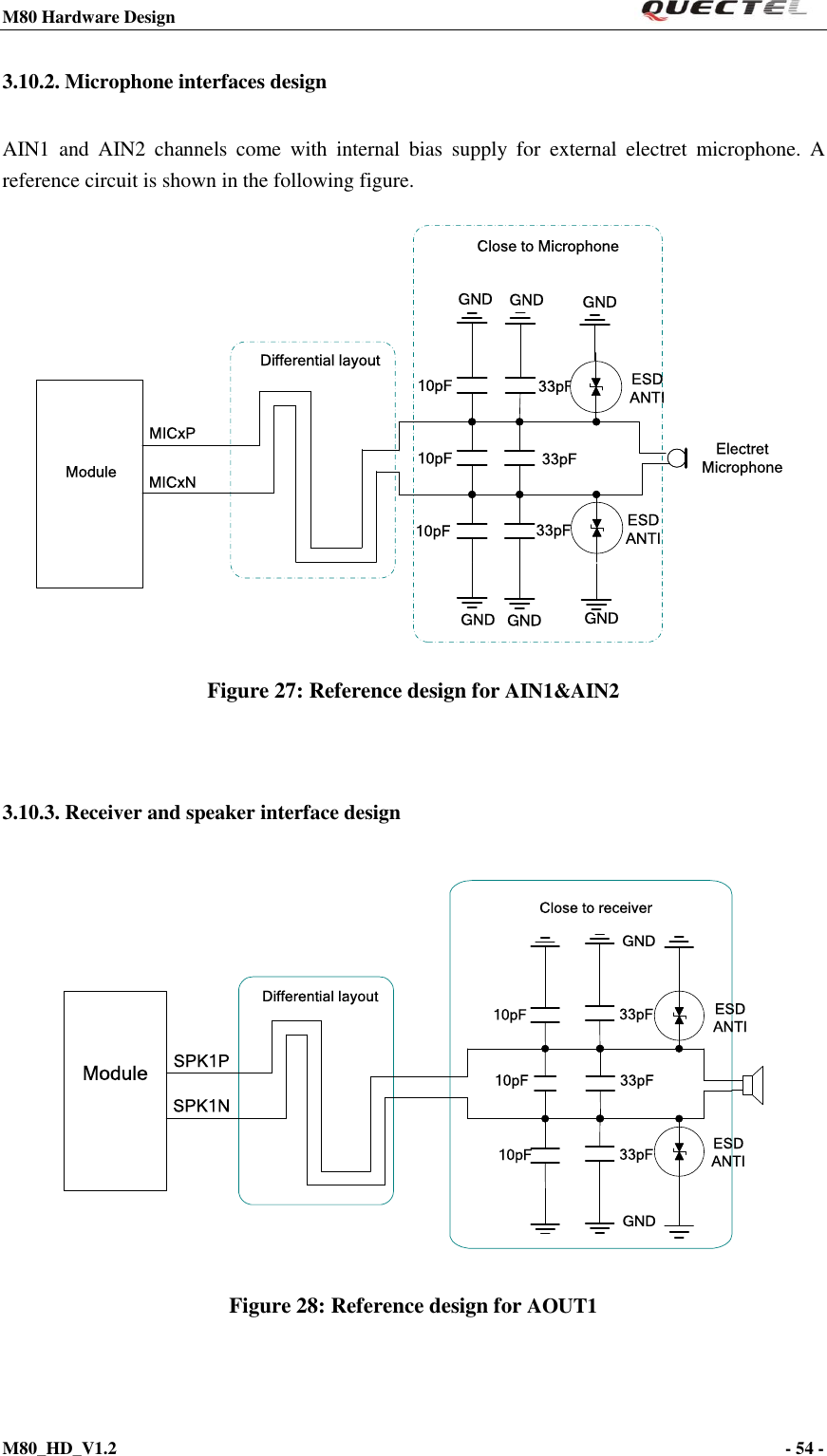
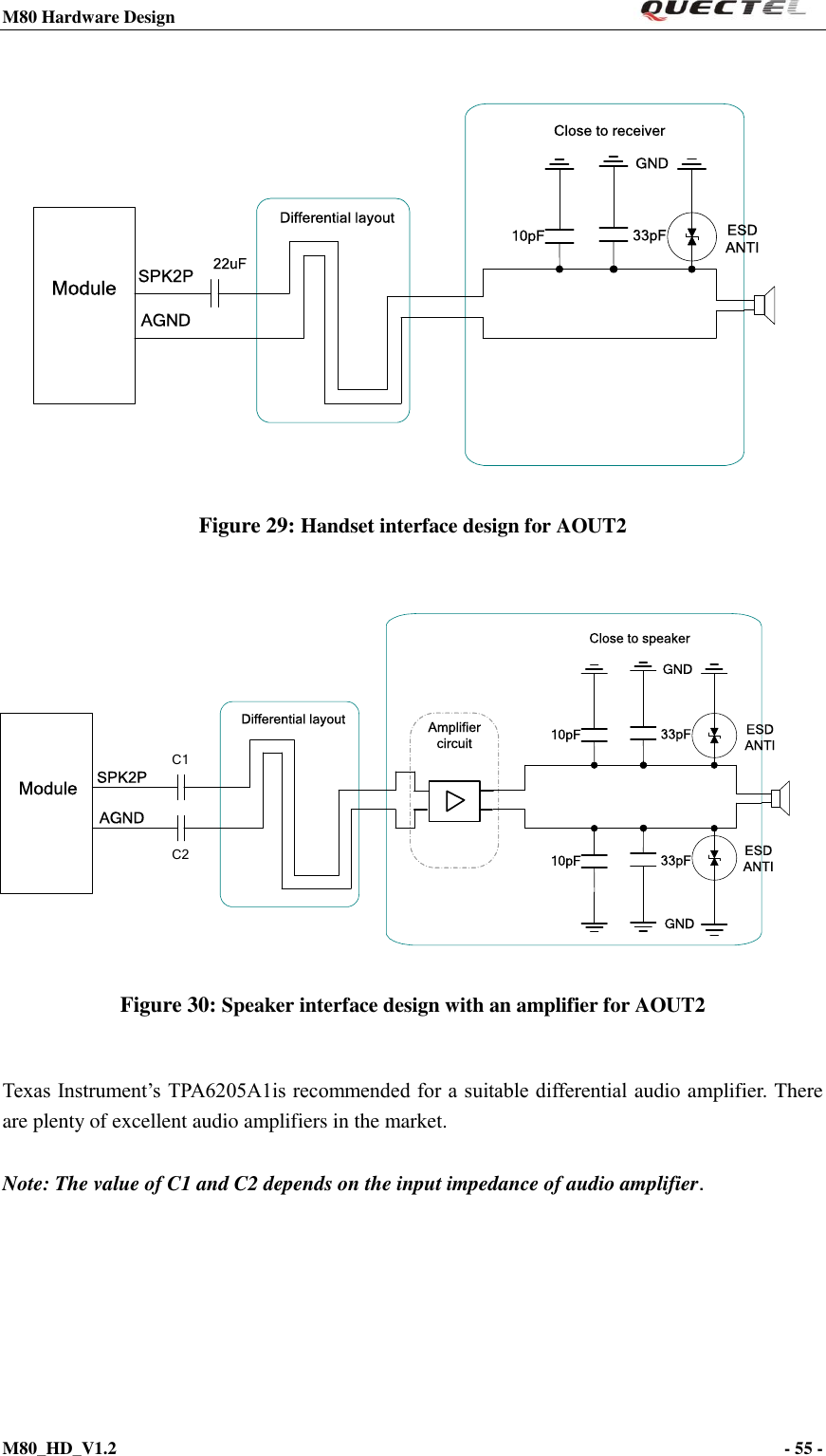
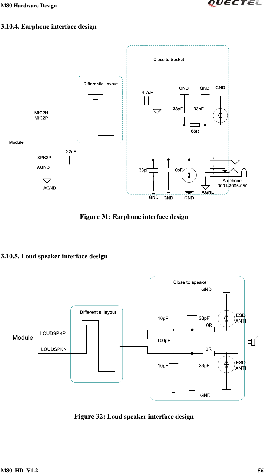
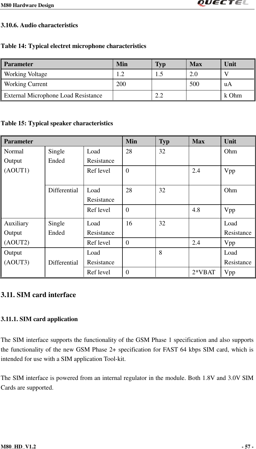
![M80 Hardware Design M80_HD_V1.2 - 52 - 3.10. Audio interfaces The module provides two analogy input channels and three analogy output channels. Table 12: Pin definition of Audio interface AIN1 and AIN2 can be used for input of microphone and line. An electret microphone is usually used. AIN1 and AIN2 are both differential input channels. AOUT1 is used for output of the receiver. This channel is typically used for a receiver built into a handset. AOUT1 channel is a differential channel. AOUT2 is typically used with earphone or speaker. It is a single-ended and mono channel. SPK2P and AGND can establish a pseudo differential mode. If customer needs to play Melody or Midi ring tone for incoming call, AOUT2 Channel should always be used. If it is used as a speaker, an amplifier should be employed also. AOUT3 is used for loud speaker output as it embedded an amplifier of class AB whose maximum drive power is 800mW. AOUT3 is a differential channel. Immediately playing Melody or Midi ring tone for incoming call is available in AOUT3. These three audio channels can be swapped by “AT+QAUDCH” command. For more details, please refer to document [1]. Use AT command “AT+QAUDCH” to select audio channel: 0--AIN1/AOUT1, the default value is 0. 1--AIN2/AOUT2 2--AIN2/AOUT3 For each channel, customer can use AT+QMIC to adjust the input gain level of microphone. Interface Name Pin Description AIN1/AOUT1 MIC1P 9 Channel one for Microphone positive input MIC1N 10 Channel one for Microphone negative input SPK1P 12 Channel one for Audio positive output SPK1N 11 Channel one for Audio negative output AIN2/AOUT2 MIC2P 7 Channel two for Microphone positive input MIC2N 8 Channel two for Microphone negative input SPK2P 5 Channel two for Audio positive output AGND 6 Cooperate with SPK2P AIN2/AOUT3 LOUDSPKP 14 Channel three for Audio positive output LOUDSPKN 13 Channel three for Audio negative output](https://usermanual.wiki/Quectel-Wireless-Solutions/201208M80/User-Guide-1783735-Page-52.png)
![M80 Hardware Design M80_HD_V1.2 - 53 - Customer can also use “AT+CLVL” to adjust the output gain level of receiver and speaker. “AT+QECHO” is used to set the parameters for echo cancellation control. “AT+QSIDET” is used to set the side-tone gain level. For more details, please refer to document [1]. Table 13: AOUT3 output characteristics Item Condition min type max unit RMS power 8ohm load VBAT=4.3v THD+N=1% 800 mW 8ohm load VBAT=3.7v THD+N=1% 700 mW 8ohm load VBAT=3.2v THD+N=1% 500 mW Gain adjustment range 0 18 dB Gain adjustment steps 3 dB 3.10.1. Decrease TDD noise and other noise The 33pF capacitor is applied for filtering out 900MHz RF interference when the module is transmitting at GSM900MHz. Without placing this capacitor, TDD noise could be heard. Moreover, the 10pF capacitor here is for filtering out 1800MHz RF interference. However, the resonant frequency point of a capacitor largely depends on the material and production technique. Therefore, customer would have to discuss with its capacitor vendor to choose the most suitable capacitor for filtering out GSM850MHz, GSM900MHz, DCS1800MHz and PCS1900MHz separately. The severity degree of the RF interference in the voice channel during GSM transmitting period largely depends on the application design. In some cases, GSM900 TDD noise is more severe; while in other cases, DCS1800 TDD noise is more obvious. Therefore, customer can have a choice based on test results. Sometimes, even no RF filtering capacitor is required. The capacitor which is used for filtering out RF noise should be close to RJ11 or other audio interfaces. Audio alignment should be as short as possible. In order to decrease radio or other signal interference, the position of RF antenna should be kept away from audio interface and audio alignment. Power alignment and audio alignment should not be parallel, and power alignment should be far away from audio alignment. The differential audio traces have to be placed according to the differential signal layout rule.](https://usermanual.wiki/Quectel-Wireless-Solutions/201208M80/User-Guide-1783735-Page-53.png)
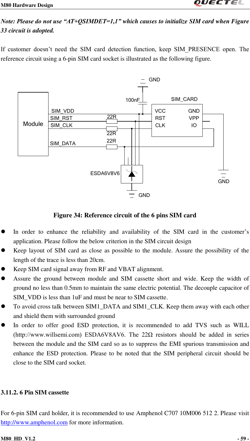
![M80 Hardware Design M80_HD_V1.2 - 58 - Table 16: Pin definition of the SIM interface In Figure 33, the pin SIM_PRESENCE is used to detect whether the tray of the Molex SIM socket, which is used for holding SIM card, is present in the card socket. When the tray is inserted in the socket, SIM_PRESENCE is at low level. Regardless of whether the SIM card is in the tray or not, the change of SIM_PRESENCE level from high to low level inspires the module to reinitialize SIM card. In default configuration, SIM card detection function is disabled. Customer’s application can use “AT+QSIMDET=1,0 ” to switch on and “AT+QSIMDET=0,0 ” to switch off the SIM card detection function. For detail of this AT command, please refer to document [1]. When “AT+QSIMDET=1,0” is set and the tray with SIM card is removed from SIM socket, the following URC will be presented. +CPIN: NOT READY When the tray with SIM card is inserted into SIM socket again and the module finishes re-initialization SIM card, the following URC will be presented. Call Ready ModuleSIM_VDDSIM_RSTSIM_CLKSIM_DATASIM_PRESENCE22R22R22RVCCRSTCLK IOVPPGNDVDD_EXT10K 100nF SIM_CARDGNDGNDESDA6V8V6GNDPRESENCE Figure 33: Reference circuit of the 8 pins SIM card Name Pin Description SIM1_VDD 56 Supply power for SIM Card. Automatic detection of SIM card voltage. 3.0V±10% and 1.8V±10%. Maximum supply current is around 10mA. SIM1_DATA 54 SIM Card data I/O SIM1_CLK 55 SIM Card clock SIM1_RST 53 SIM Card reset SIM_PRESENCE 57 SIM Card detect SIM1_GND 52 SIM Card ground](https://usermanual.wiki/Quectel-Wireless-Solutions/201208M80/User-Guide-1783735-Page-58.png)
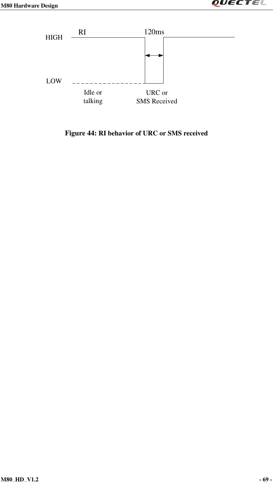
![M80 Hardware Design M80_HD_V1.2 - 67 - 3.14. ADC The module provides two ADC to measure the value of voltage. The command “AT+QADC” can read the voltage value applied on ADC0 pin, while AT command “AT+QEADC” can read the voltage value applied on ADC1 pin. For details of this AT command, please refer to document [1]. In order to improve the accuracy of ADC, the layout of ADC should be surrounded by ground. Table 24: Pin definition of the ADC Name Pin Description ADC0 2 Analog to digital converter. ADC1 1 Analog to digital converter. Table 25: Characteristics of the ADC Item Min Typ Max Units Voltage Range 0 2.8 V ADC Resolution 10 bits ADC Accuracy 2.7 mV 3.15. Behaviors of the RI Table 26: Behaviors of the RI State RI response Standby HIGH Voice calling Change to LOW, then: 1. Change to HIGH when call is established. 2. Use ATH to hang up the call, RI changes to HIGH. 3. Calling part hangs up, RI changes to HIGH first, and changes to LOW for 120ms indicating “NO CARRIER” as an URC, then changes to HIGH again. 4. Change to HIGH when SMS is received. Data calling Change to LOW, then: 1. Change to HIGH when data connection is established. 2. Use ATH to hang up the data calling, RI changes to HIGH. 3. Calling part hangs up, RI changes to HIGH first, and changes to LOW for 120ms indicating “NO CARRIER” as an URC, then changes to HIGH again. 4. Change to HIGH when SMS is received.](https://usermanual.wiki/Quectel-Wireless-Solutions/201208M80/User-Guide-1783735-Page-67.png)
![M80 Hardware Design M80_HD_V1.2 - 68 - SMS When a new SMS comes, the RI changes to LOW and holds low level for about 120 ms, then changes to HIGH. URC Certain URCs can trigger 120ms low level on RI. For more details, please refer to the document [1] If the module is used as a caller, the RI would maintain high except the URC or SMS is received. On the other hand, when it is used as a receiver, the timing of the RI is shown below. RIIdle RingOff-hook by “ATA”. On-hook by “ATH”. SMS received. HIGHLOW Figure 41: RI behavior of voice calling as a receiver RIIdle RingData calling establish. On-hook by “ATH”. SMS receivedHIGHLOW Figure 42: RI behavior of data calling as a receiver RIIdle Calling On-hookTalkingHIGHLOWIdle Figure 43: RI behavior as a caller](https://usermanual.wiki/Quectel-Wireless-Solutions/201208M80/User-Guide-1783735-Page-68.png)