Quectel Wireless Solutions 201404UC15 UMTS/HSDPA Module User Manual
Quectel Wireless Solutions Company Limited UMTS/HSDPA Module
UserManual.wiki
>
Quectel Wireless Solutions
>
201404UC15 User Manual
>
User Manual
Contents
1.
User Manual
2.
Quectel_UC15_User_Manual
User Manual
Navigation menu
Upload a User Manual
Namespaces
Wiki Guide
HTML
PDF
Info
Views
User Manual
Discussion / Help
Navigation
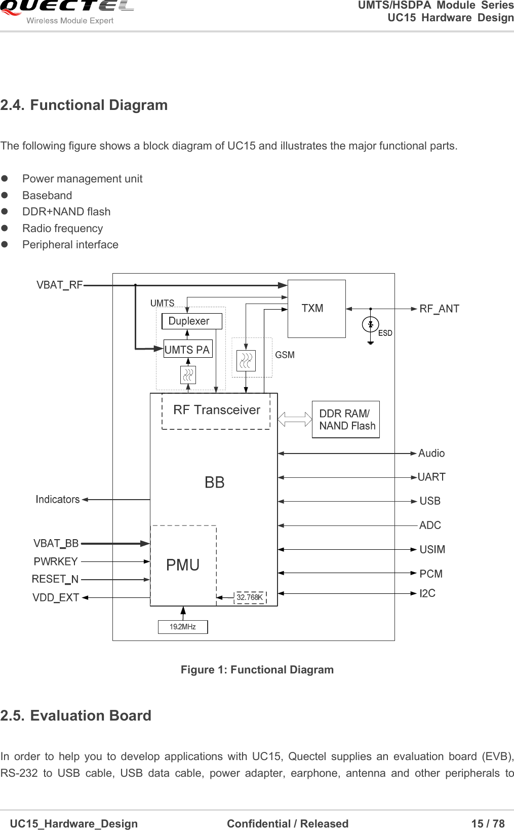
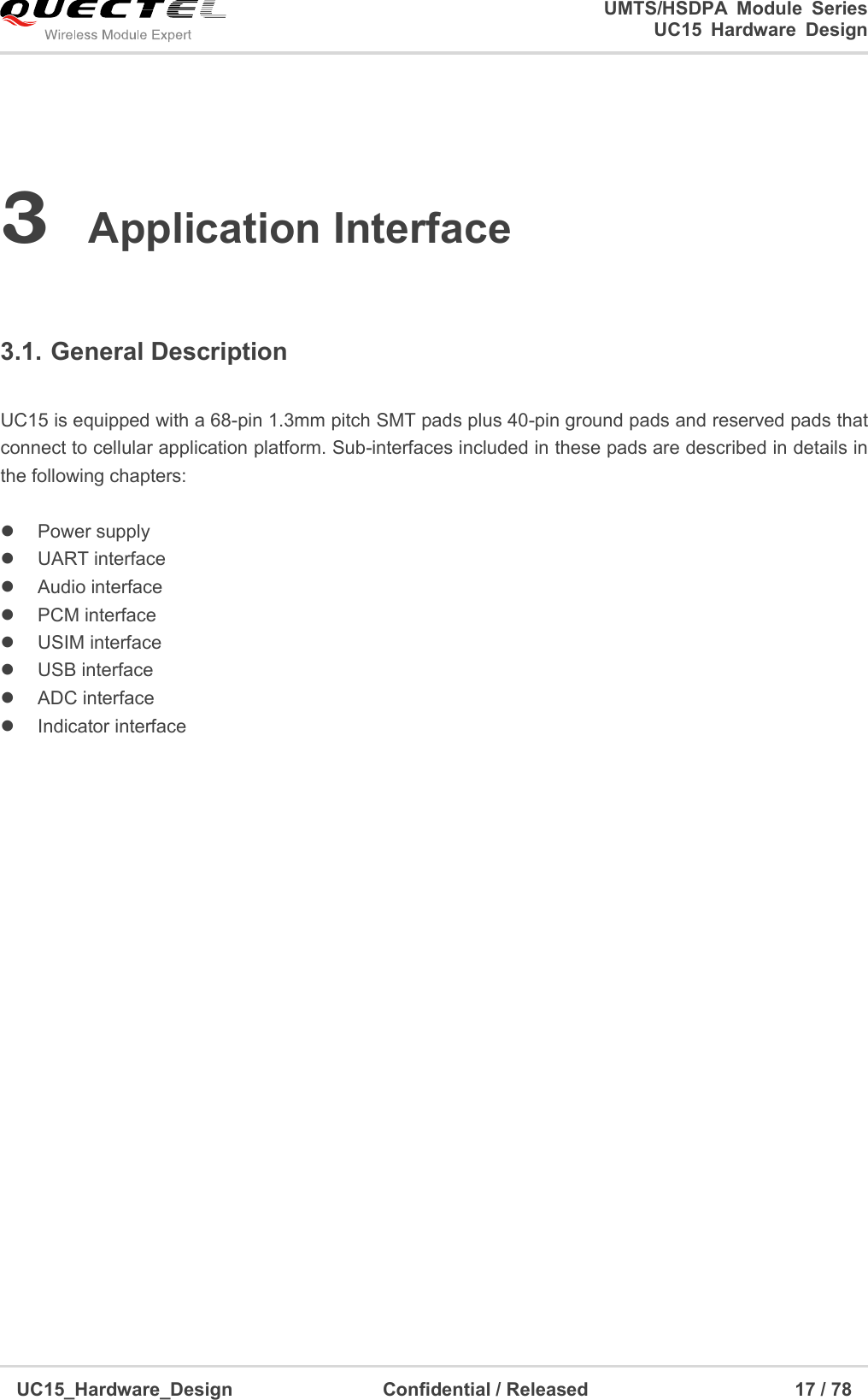
![UMTS/HSDPA Module Series UC15 Hardware Design UC15_Hardware_Design Confidential / Released 16 / 78 control or test the module. For details, please refer to document [2].](https://usermanual.wiki/Quectel-Wireless-Solutions/201404UC15.User-Manual/User-Guide-2280271-Page-17.png)
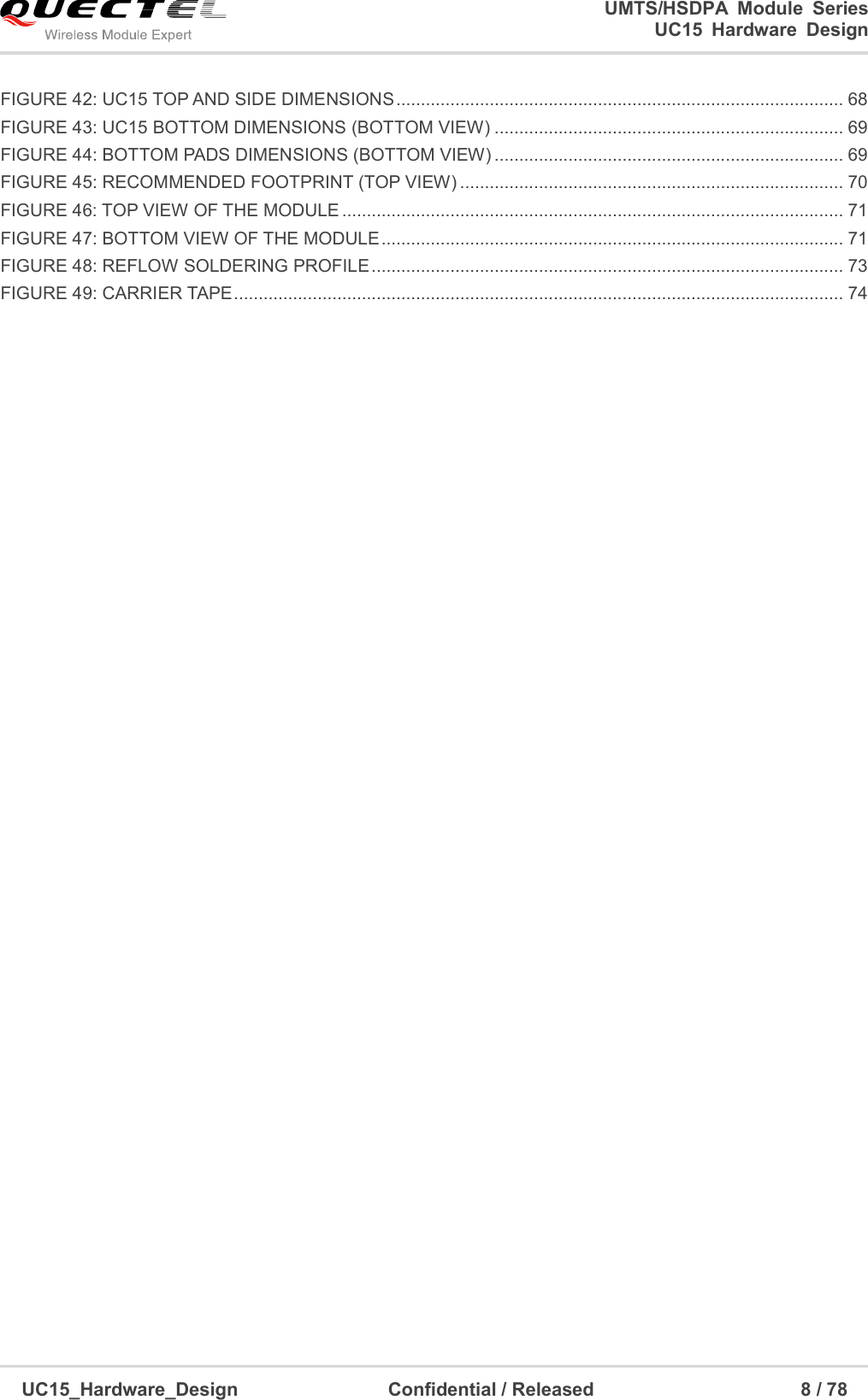
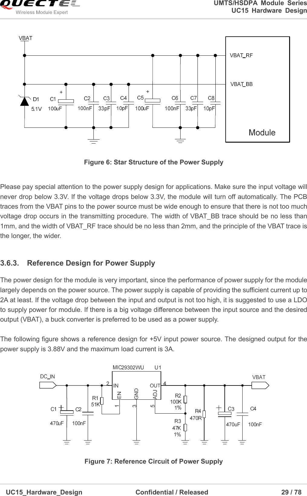
![UMTS/HSDPA Module Series UC15 Hardware Design UC15_Hardware_Design Confidential / Released 28 / 78 AT+CFUN=4: Disable RF function (airplane mode). All AT commands related to RF function are not accessible. For detailed information about command AT+CFUN, please refer to document [1]. 3.6. Power Supply 3.6.1. Power Supply Pins UC15 provides four VBAT pins to connect with the external power supply. There are two separate voltage domains for VBAT. VBAT_RF with two pads for module RF. VBAT_BB with two pads for module baseband. The following table shows the VBAT pins and ground pins. Table 6: VBAT and GND Pin 3.6.2. Decrease Voltage Drop The power supply range of the module is 3.3~4.3V. Because of the voltage drop during the transmitting time, a bypass capacitor of about 100µF with low ESR should be used. Multi-layer ceramic chip (MLCC) capacitor can provide the best combination of low ESR. Three ceramic capacitors (100nF, 33pF, 10pF) are recommended to be applied to the VBAT pins. The capacitors should be placed close to the VBAT pins of UC15. The following figure shows star structure of the power supply. The main power supply from an external application should be a single voltage source and has to be expanded to two sub paths with star structure. In addition, in order to get a stable power source, it is suggested to use a zener diode of which reverse zener voltage is 5.1V and dissipation power is more than 0.5W. Pin Name Pin No. Description Min. Typ. Max. Unit VBAT_RF 50,51 Power supply for module RF. 3.3 3.8 4.3 V VBAT_BB 52,53 Power supply for module baseband. 3.3 3.8 4.3 V GND 42,44~49,65, 67~68,81~108 Ground. - - - -](https://usermanual.wiki/Quectel-Wireless-Solutions/201404UC15.User-Manual/User-Guide-2280271-Page-29.png)
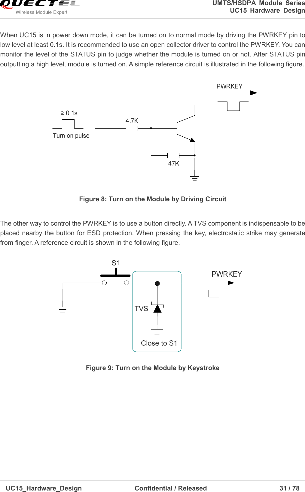
![UMTS/HSDPA Module Series UC15 Hardware Design UC15_Hardware_Design Confidential / Released 30 / 78 3.6.4. Monitor the Power Supply You can use the AT+CBC command to monitor the VBAT_BB voltage value. For more details, please refer to document [1]. 3.6.5. VDD_EXT UC15 has a LDO power output, named VDD_EXT. The VDD_EXT is available and output voltage is 2.6V by default, rated at 100mA. The following table shows electrical characteristics of VDD_EXT. Table 7: Electrical Characteristics of VDD_EXT 3.7. Turn on and off Scenarios 3.7.1. Turn on Module by PWRKEY Pin The following table shows the pin definition of PWRKEY. Table 8: PWRKEY Pin Description Symbol Description Min. Typ. Max. Unit VDD_EXT Output voltage 2.5 2.6 2.7 V IOUT Output current - - 100 mA Pin Name Pin No. Description DC Characteristics Comment PWRKEY 18 Turn on/off the module. VIHmax=2.1V VIHmin=1.6V VILmax=0.5V Pull-up to 1.8V internally with 200kΩ resistor.](https://usermanual.wiki/Quectel-Wireless-Solutions/201404UC15.User-Manual/User-Guide-2280271-Page-31.png)
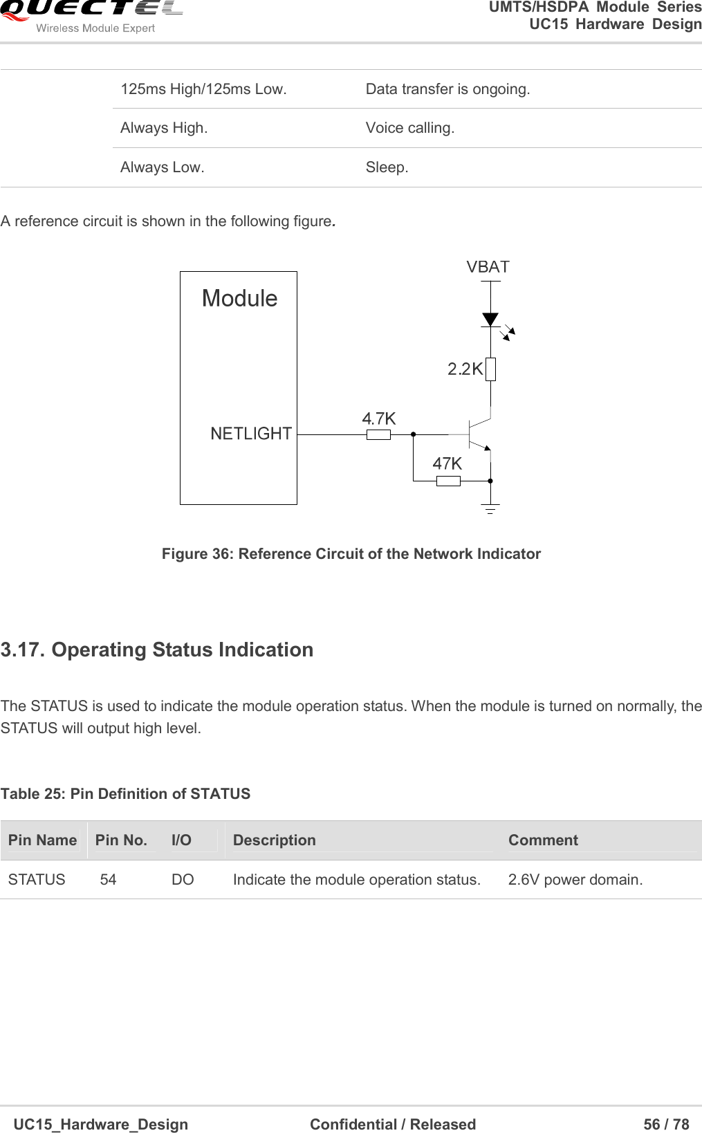
![UMTS/HSDPA Module Series UC15 Hardware Design UC15_Hardware_Design Confidential / Released 33 / 78 Figure 11: Timing of Turning off Module During power-down procedure, module will send out URC “NORMAL POWER DOWN” via URC port first, then log off network and save important data. After logging off, module sends out “POWERED DOWN” and shuts down the internal power supply. The power on VBAT pins are not allowed to be switched off before the URC “POWERED DOWN” is output to avoid data loss. If module is not logged off within 60s, module will force to shut down internal power supply. After that moment, the module enters into power down mode, no other AT commands can be executed. The power down mode can also be indicated by the STATUS pin. 3.7.2.2. Turn off Module by AT Command It is also a safe way to use AT command AT+QPOWD to turn off the module, which is similar to the way of turning off the module via PWRKEY Pin. Please refer to document [1] for details about the AT command of AT+QPOWD. 3.7.2.3. Automatic Shutdown The module will constantly monitor the voltage applied on the VBAT_BB, if the voltage ≤ 3.5V, the following URC will be presented: +QIND: “vbatt”,-1 If the voltage ≥ 4.21V, the following URC will be presented: +QIND: “vbatt”,1 The uncritical voltage is 3.3V to 4.3V, If the voltage > 4.35V or < 3.2V, the module would automatically shut down itself.](https://usermanual.wiki/Quectel-Wireless-Solutions/201404UC15.User-Manual/User-Guide-2280271-Page-34.png)
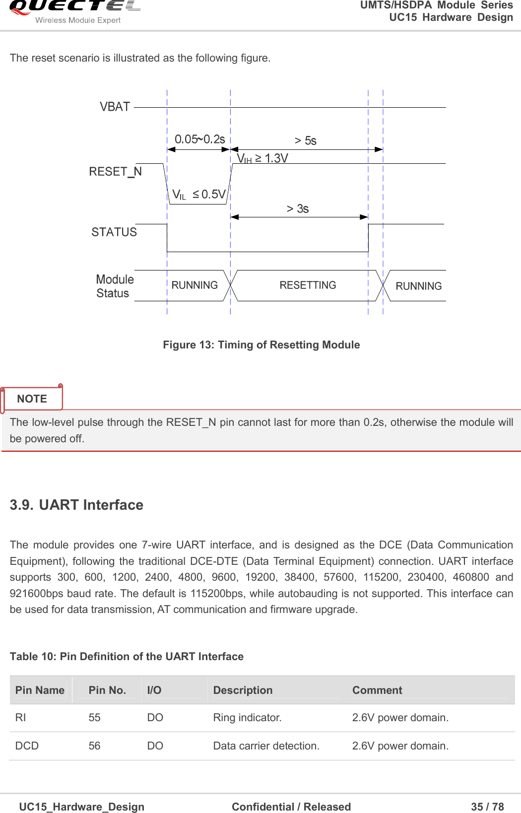
![UMTS/HSDPA Module Series UC15 Hardware Design UC15_Hardware_Design Confidential / Released 34 / 78 If the voltage < 3.2V, the following URC will be presented: +QIND: “vbatt”,-2 If the voltage > 4.35V, the following URC will be presented: +QIND: “vbatt”,2 The value of voltage threshold can be revised by AT command AT+QCFG=“vbatt”, refer to document [1] for details. 3.8. Reset the Module The RESET_N can be used to reset the module. Table 9: RESET_N Pin Description You can reset the module by driving the RESET_N to low level voltage for 0.05~0.2s and then releasing. A reference circuit is shown in the following figure. Figure 12: Reference Circuit of RESET_N Pin Name Pin No. Description DC Characteristics Comment RESET_N 17 Reset the module. VIHmax=2.1V VIHmin=1.6V VILmax=0.5V Pull-up to 1.8V internally. NOTE](https://usermanual.wiki/Quectel-Wireless-Solutions/201404UC15.User-Manual/User-Guide-2280271-Page-35.png)
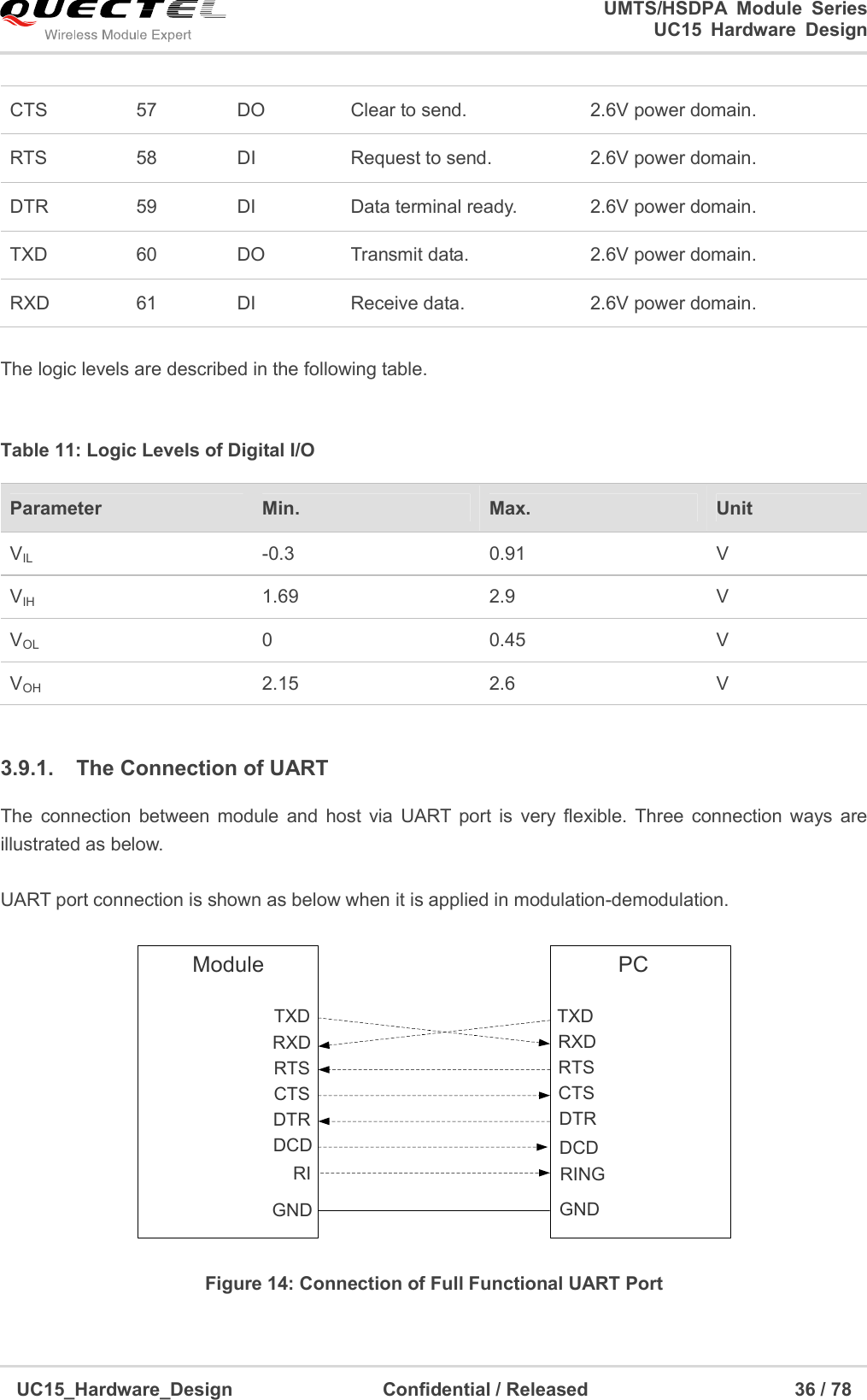
![UMTS/HSDPA Module Series UC15 Hardware Design UC15_Hardware_Design Confidential / Released 37 / 78 Three lines connection is shown as below. Figure 15: Connection of Three Lines UART Port UART port with hardware flow control is shown as below. This connection will enhance the reliability of the mass data communication. Figure 16: Connection of UART Port with Hardware Flow Control The module disables the hardware flow control by default. AT command AT+IFC=2,2 is used to enable hardware flow control. AT command AT+IFC=0,0 is used to disable the hardware flow control. For more details, please refer to document [1]. NOTE](https://usermanual.wiki/Quectel-Wireless-Solutions/201404UC15.User-Manual/User-Guide-2280271-Page-38.png)
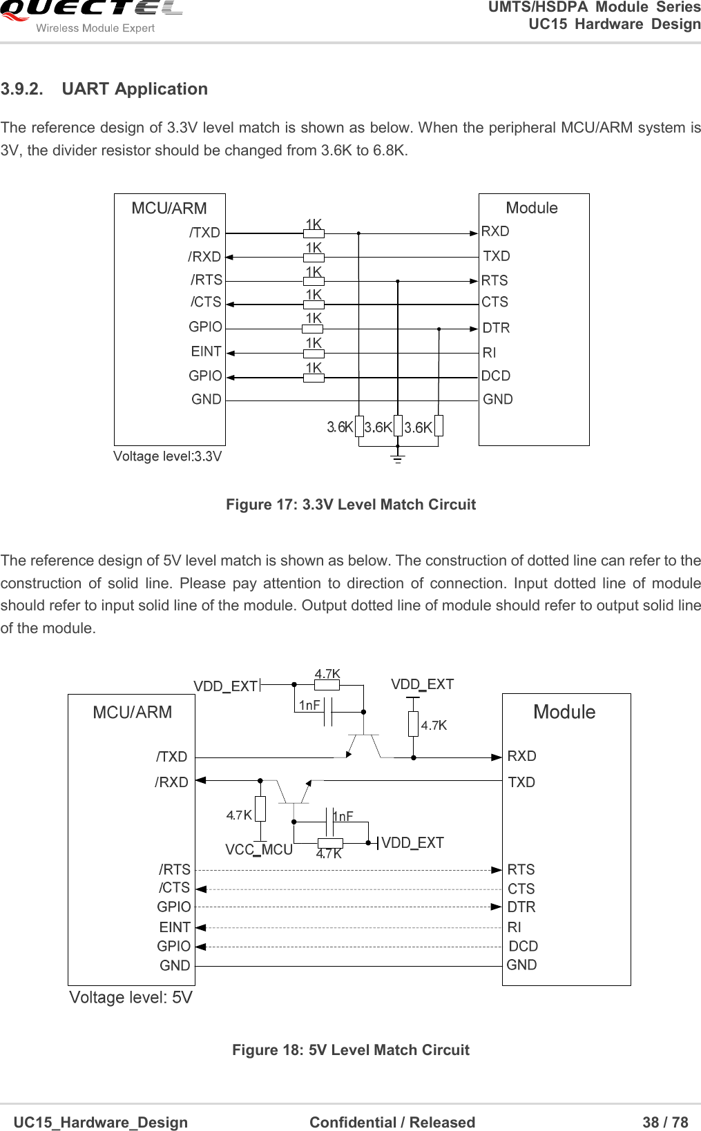
![UMTS/HSDPA Module Series UC15 Hardware Design UC15_Hardware_Design Confidential / Released 39 / 78 The following figure is an example of connection between module and PC. A RS232 level shifter IC or circuit must be inserted between module and PC, since UART interface do not support the RS232 level, while support the CMOS level only. Figure 19: RS232 Level Shift Circuit 1. Rising edge on DTR will let the module exit from the data mode by default. It can be disabled by command. Refer to document [1] about AT&D and AT&V for details. 2. DCD is used as data mode indication. Please refer to document [1] about command AT&C and AT&V for details. 3.10. Behavior of the RI You can use command AT+QCFG=“risignaltype”, “physical” to configure RI behavior: No matter which port URC is presented on, URC will trigger the behavior on RI pin. NOTES](https://usermanual.wiki/Quectel-Wireless-Solutions/201404UC15.User-Manual/User-Guide-2280271-Page-40.png)
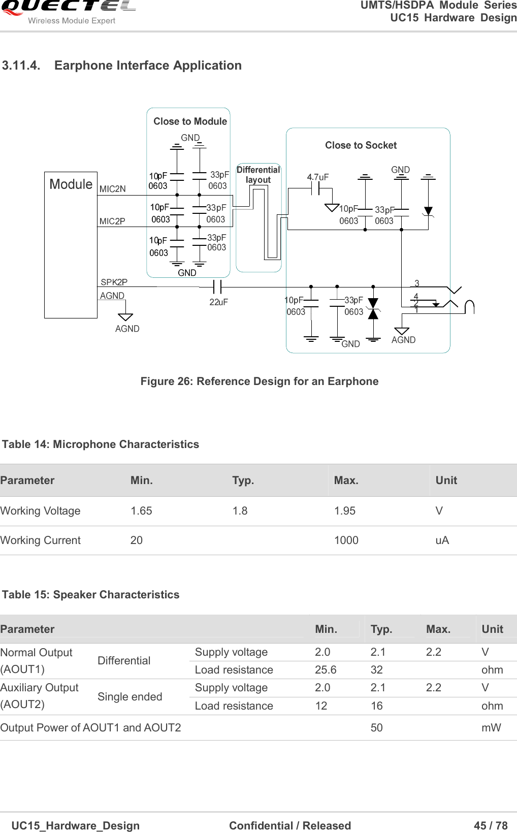
![UMTS/HSDPA Module Series UC15 Hardware Design UC15_Hardware_Design Confidential / Released 40 / 78 URC can be output from UART port, USB AT port and USB modem port by command AT+QURCCFG. The default port is USB AT port. In additional, RI behavior can be configured flexible. The default behavior of the RI is shown as below. Table 12: Behavior of the RI Figure 20: RI Behavior The RI behavior can be changed by command AT+QCFG=“urc/ri/ring”, refer to document [1] for details. 3.11. Analog Audio Interface The module provides two analog input channels and two analog output channels. Table 13: Pin Definition of the Audio Interface State Response Idle RI keeps in high level. URC RI outputs 120ms low pulse when new URC is reported. Interface Pin Name Pin No. I/O Description Comment AIN1/ MIC1P 23 AI Audio positive input. If it is unused, keep open. NOTE](https://usermanual.wiki/Quectel-Wireless-Solutions/201404UC15.User-Manual/User-Guide-2280271-Page-41.png)
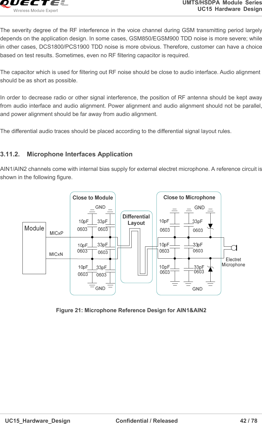
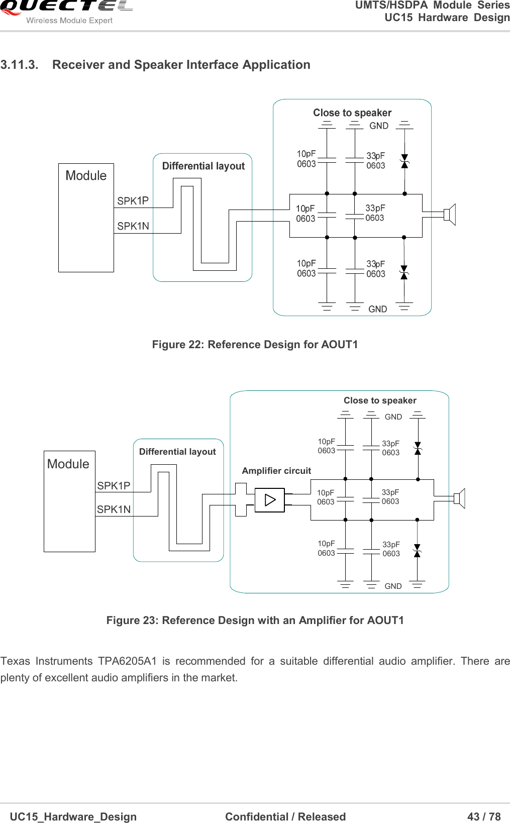
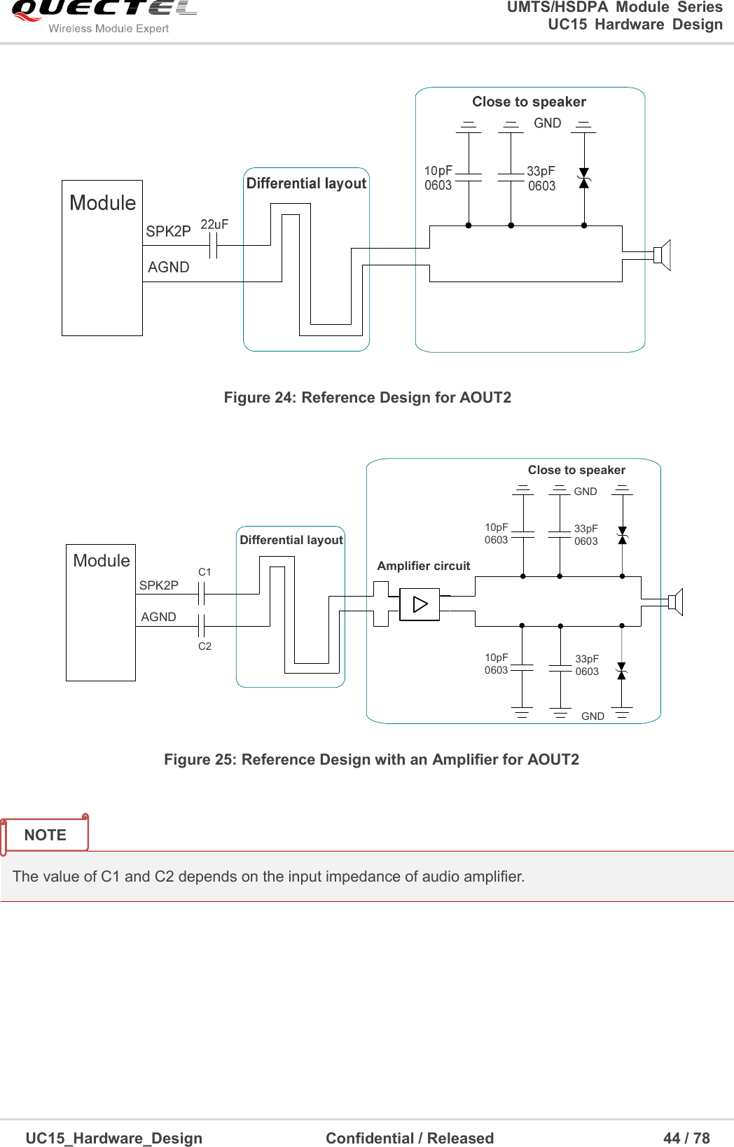
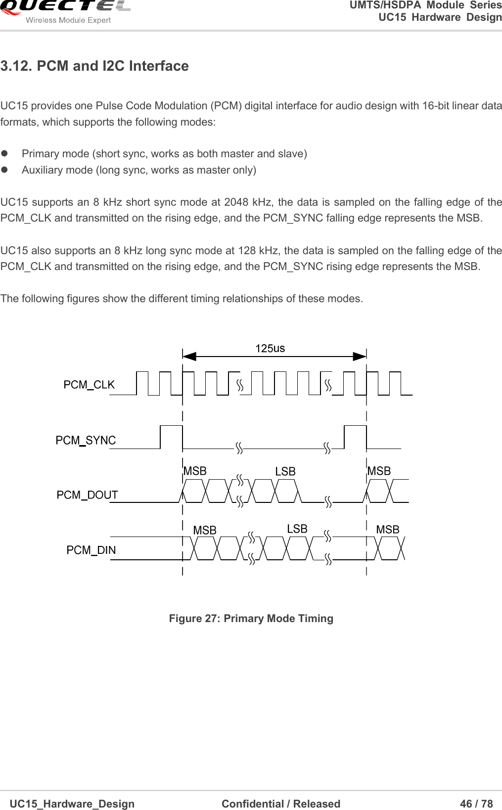
![UMTS/HSDPA Module Series UC15 Hardware Design UC15_Hardware_Design Confidential / Released 41 / 78 AIN1 and AIN2 may be used for both microphone and line inputs. An electret microphone is usually recommended. AIN1 and AIN2 are both differential input channels. AOUT1 and AOUT2 may be used for both receiver and speaker outputs. AOUT1 channel is typically used for a receiver, while AOUT2 channel is typically used for headset or speaker. AOUT1 channel is a differential channel and AOUT2 is a single-ended channel. SPK2P and AGND can establish a pseudo differential mode. Both AOUT1 and AOUT2 support voice and ringtone output, and so on. These two audio channels can be swapped by AT+QAUDPATH command. For more details, please refer to document [1]. Use command AT+QAUDPATH to select audio channel: 0: AIN1/AOUT1 (normal audio channel), the default value is 0. 1: AIN2/AOUT2 (auxiliary audio channel). 2: PCM channel. For each channel, you can use AT+QMIC to adjust the input gain level of microphone. You can also use AT+CLVL to adjust the output gain level of receiver and speaker. AT+QSIDET is to set the side-tone gain level. For more details, please refer to document [1]. 3.11.1. Decrease TDD Noise and Other Noise The 33pF capacitor is applied for filtering out 900MHz RF interference when the module is transmitting at GSM900/EGSM900MHz. TDD noise could be heard without this capacitor. Moreover, the 10pF capacitor here is for filtering out 1800/1900MHz RF interference. However, the self-resonant frequency point of a capacitor largely depends on the material and production technique. Therefore, customer should depend on its capacitor vendor to choose the most suitable capacitor for filtering out GSM850MHz, EGSM900MHz, DCS1800MHz and PCS1900MHz separately. AOUT1 MIC1N 24 AI Audio negative input. If it is unused, keep open. SPK1P 22 AO Audio positive output. If it is unused, keep open. SPK1N 21 AO Audio negative output. If it is unused, keep open. AIN2/ AOUT2 MIC2P 25 AI Auxiliary audio positive input. If it is unused, keep open. MIC2N 26 AI Auxiliary audio negative input. If it is unused, keep open. SPK2P 20 AO Auxiliary audio positive output. If it is unused, keep open. AGND 19 Analog ground. Suggested to be used for audio circuit.](https://usermanual.wiki/Quectel-Wireless-Solutions/201404UC15.User-Manual/User-Guide-2280271-Page-42.png)
![UMTS/HSDPA Module Series UC15 Hardware Design UC15_Hardware_Design Confidential / Released 47 / 78 Figure 28: Auxiliary Mode Timing The following table shows the pin definition of PCM and I2C interface which can be applied on audio codec design. Table 16: Pin Definition of PCM and I2C Interface UC15’s firmware has integrated the configuration on NAU8814 application with I2C interface. The default configuration is master mode which uses short sync data format with 2048 kHz clock. Please refer to document [1] for details about the command AT+QDAI. Pin Name Pin No. I/O Description Comment PCM_DOUT 34 DO PCM data output. 2.6V power domain PCM_DIN 35 DI PCM data input. 2.6V power domain PCM_CLK 36 IO PCM data bit clock. 2.6V power domain PCM_SYNC 37 DO PCM data frame sync signal 2.6V power domain I2C_SDA 38 IO I2C serial data. External pull-up resistor is required. 2.6V only. I2C_SCL 39 DO I2C serial clock. External pull-up resistor is required. 2.6V only.](https://usermanual.wiki/Quectel-Wireless-Solutions/201404UC15.User-Manual/User-Guide-2280271-Page-48.png)
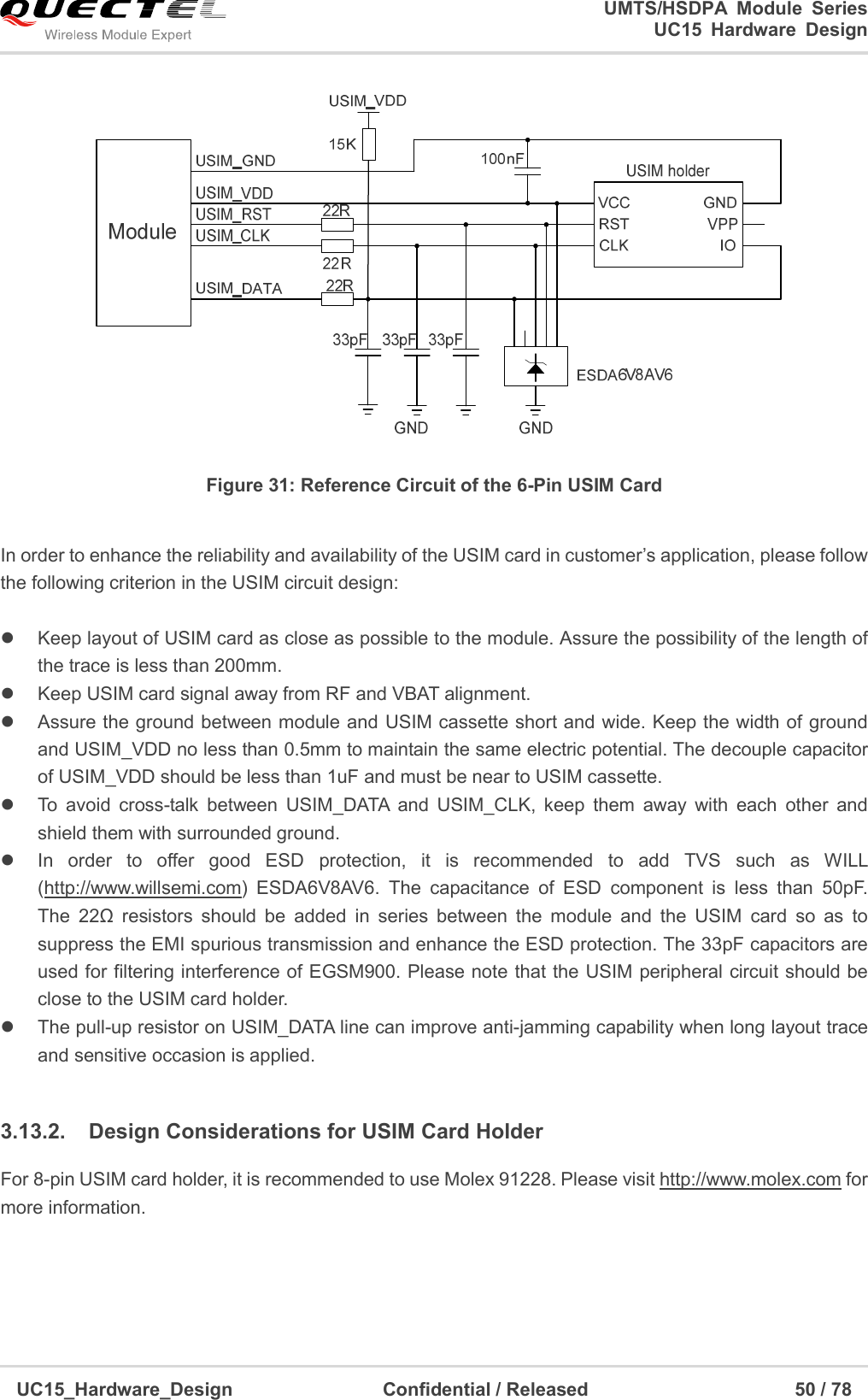
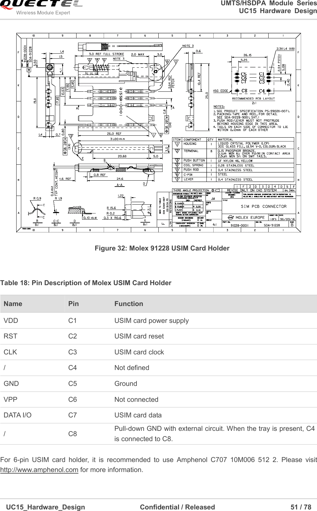
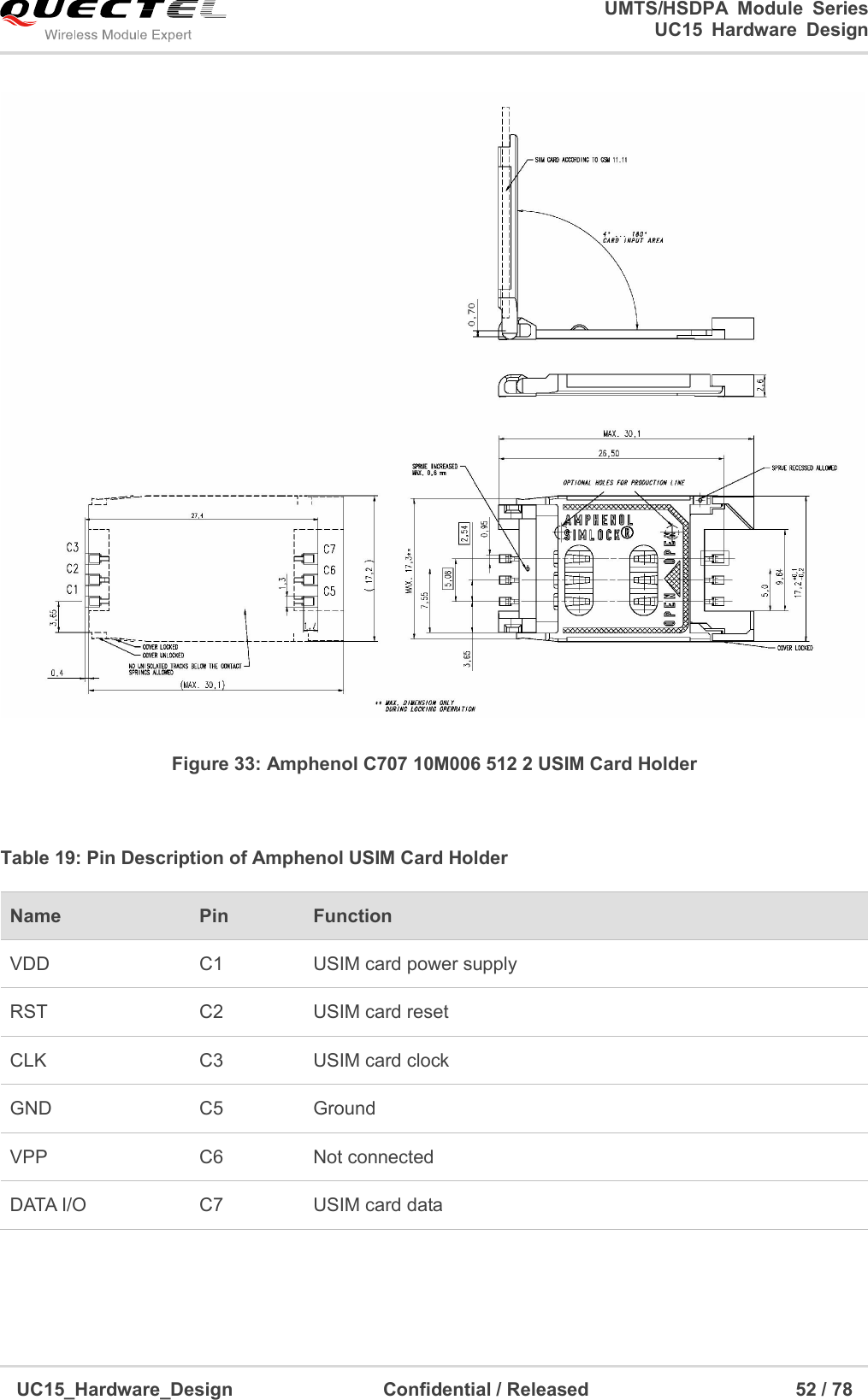
![UMTS/HSDPA Module Series UC15 Hardware Design UC15_Hardware_Design Confidential / Released 49 / 78 The following figure shows the reference design of the 8-pin USIM card. ModuleUSIM_VDDUSIM_GNDUSIM_RSTUSIM_CLKUSIM_DATAUSIM_PRESENCE22R22R22RVDD_EXT51K100nF USIM holderGNDGNDESDA6V8AV633pF 33pF 33pFVCCRSTCLK IOVPPGNDGNDUSIM_VDD15K Figure 30: Reference Circuit of the 8-Pin USIM Card Some AT commands are invalid when USIM card is not applied. UC15 supports USIM card hot-plugging via the USIM_PRESENCE pin. For details, refer to document [1] about the command AT+QSIMDET. If you do not need the USIM card detection function, keep USIM_PRESENCE unconnected. The reference circuit for using a 6-pin USIM card holder is illustrated as the following figure. USIM_CLK 14 DO Clock signal of USIM card. USIM_RST 15 DO Reset signal of USIM card. USIM_ PRESENCE 11 DI USIM card detection input. 2.6V power domain USIM_GND 8 Specified ground for USIM card. NOTE](https://usermanual.wiki/Quectel-Wireless-Solutions/201404UC15.User-Manual/User-Guide-2280271-Page-50.png)
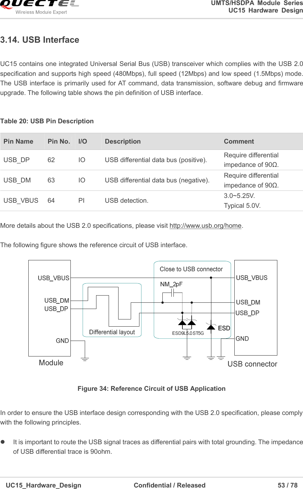
![UMTS/HSDPA Module Series UC15 Hardware Design UC15_Hardware_Design Confidential / Released 54 / 78 Keep the ESD components as closer to the USB connector as possible. Pay attention to the influence of junction capacitance of ESD component on USB data lines. Typically, the capacitance value should be less than 2pF such as ESD9L5.0ST5G. Do not route signal traces under crystals, oscillators, magnetic devices and RF signal traces. It is important to route the USB differential traces in inner-layer with ground shielding not only upper and lower layer but also right and left side. UC15 module can only be used as a slave device. The USB interface is recommended to be reserved for firmware upgrade in your design. The following figure shows the recommended test points. Figure 35: Test Points of Firmware Upgrade 3.15. ADC Function The module provides two analog-to-digital converters (ADC) to digitize the analog signal to 12-bit digital data. Using AT command AT+QADC=0 can read the voltage value on ADC0 pin. Using AT command AT+QADC=1 can read the voltage value on ADC1 pin. For more details of these AT commands, please refer to document [1]. In order to improve the accuracy of ADC, the trace of ADC should be surrounded by ground. NOTE](https://usermanual.wiki/Quectel-Wireless-Solutions/201404UC15.User-Manual/User-Guide-2280271-Page-55.png)
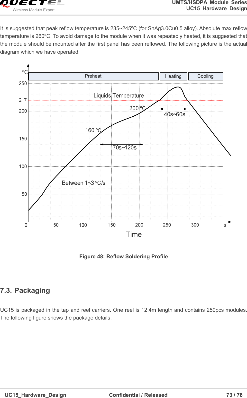
![UMTS/HSDPA Module Series UC15 Hardware Design UC15_Hardware_Design Confidential / Released 72 / 78 7 Storage and Manufacturing 7.1. Storage UC15 is stored in the vacuum-sealed bag. The restriction of storage condition is shown as below. Shelf life in sealed bag is 12 months at < 40ºC/90%RH. After this bag is opened, devices that will be subjected to reflow solder or other high temperature process must be: Mounted within 72 hours at factory conditions of ≤ 30ºC/60%RH. Stored at < 10% RH. Devices require bake, before mounting, if: Humidity indicator card is > 10% when read 23ºC±5ºC. Mounted for more than 72 hours at factory conditions of ≤ 30ºC/60% RH. If baking is required, devices may be baked for 48 hours at 125ºC±5ºC. As plastic container cannot be subjected to high temperature, module needs to be taken out from container to high temperature (125ºC) bake. If shorter bake times are desired, please refer to IPC/JEDECJ-STD-033 for bake procedure. 7.2. Manufacturing and Welding The squeegee should push the paste on the surface of the stencil that makes the paste fill the stencil openings and penetrate to the PCB. The force on the squeegee should be adjusted so as to produce a clean stencil surface on a single pass. To ensure the module soldering quality, the thickness of stencil at the hole of the module pads should be 0.18mm. For details, please refer to document [4]. NOTE](https://usermanual.wiki/Quectel-Wireless-Solutions/201404UC15.User-Manual/User-Guide-2280271-Page-73.png)
![UMTS/HSDPA Module Series UC15 Hardware Design UC15_Hardware_Design Confidential / Released 75 / 78 8 Appendix A Reference Table 36: Related Documents Table 37: Terms and Abbreviations SN Document Name Remark [1] Quectel_UC15_AT_Commands_Manual UC15 AT commands manual [2] Quectel_M10_EVB_User_Guide M10 EVB user guide [3] Quectel_UC15_Reference_Design UC15 reference design [4] Quectel_Module_Secondary_SMT_User_Guide Module secondary SMT user guide Abbreviation Description AMR Adaptive Multi-rate bps Bits Per Second CHAP Challenge Handshake Authentication Protocol CS Coding Scheme CSD Circuit Switched Data CTS Clear to Send DRX Discontinuous Reception DCE Data Communications Equipment (typical module) DTE Data Terminal Equipment (typical computer, external controller) DTR Data Terminal Ready DTX Discontinuous Transmission](https://usermanual.wiki/Quectel-Wireless-Solutions/201404UC15.User-Manual/User-Guide-2280271-Page-76.png)