Quectel Wireless Solutions 201404UC15M UMTS/HSDPA module User Manual Manual
Quectel Wireless Solutions Company Limited UMTS/HSDPA module Manual
UserManual.wiki
>
Quectel Wireless Solutions
>
201404UC15M User Manual
Manual
Navigation menu
Upload a User Manual
Namespaces
Wiki Guide
HTML
PDF
Info
Views
User Manual
Discussion / Help
Navigation
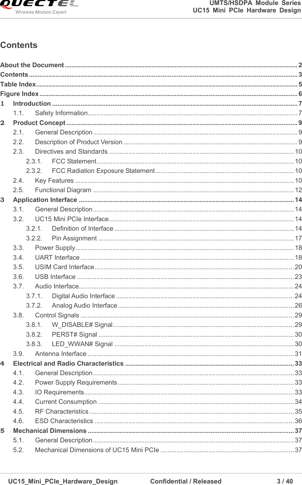
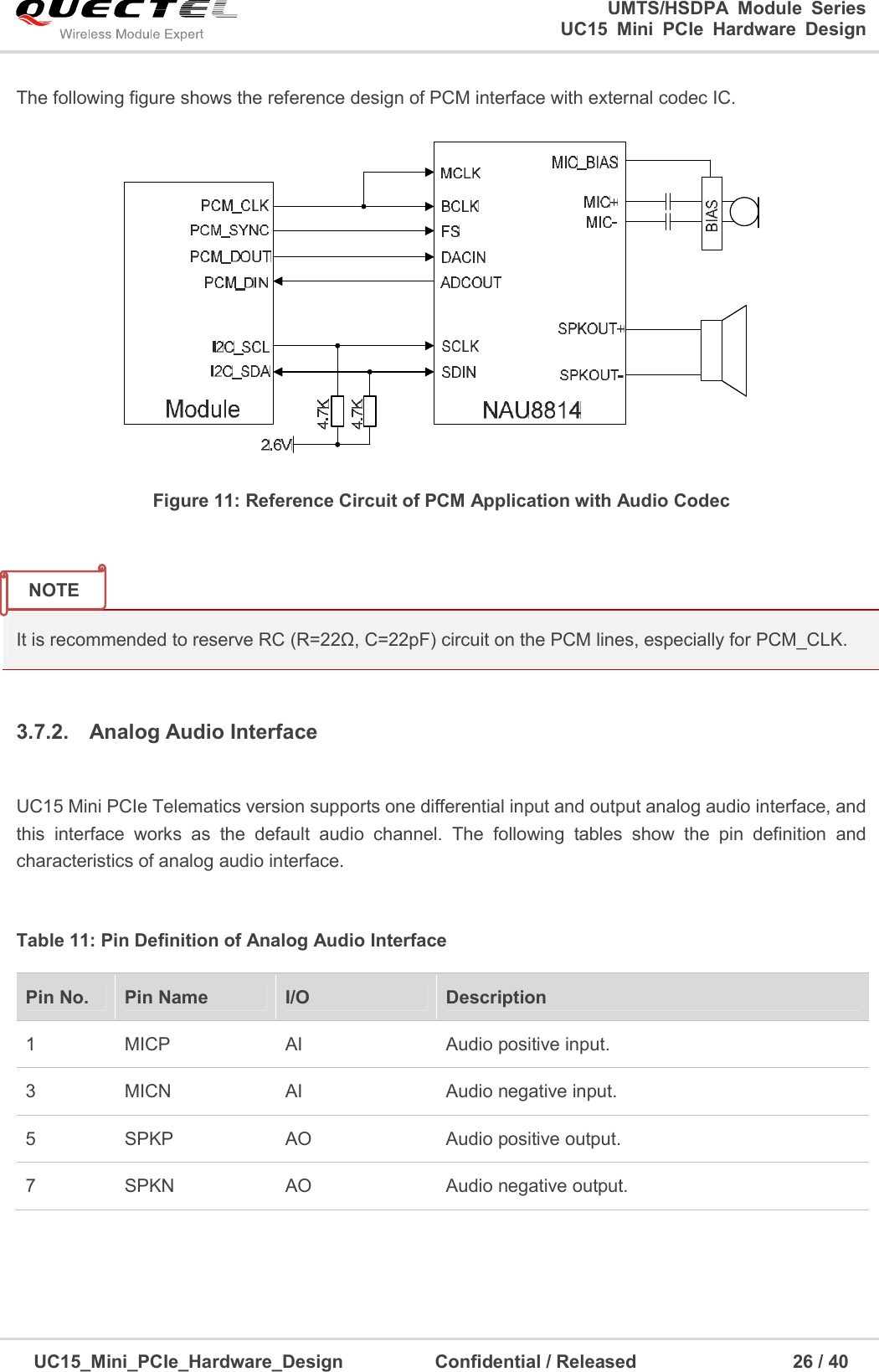
![UMTS/HSDPA Module Series UC15 Mini PCIe Hardware Design UC15_Mini_PCIe_Hardware_Design Confidential / Released 20 / 40 Figure 5: RS232 Level Match Circuit 1. The hardware flow control is disabled by default. AT command AT+IFC=2,2 is used to enable the hardware flow control. AT command AT+IFC=0,0 is used to disable the hardware flow control. For more details, please refer to document [2]. 2. AT command AT+IPR is used to set the baud rate of the UART. Please refer to document [2] for details. 3. UART_DTR supports sleep control function. Driving it to low level will wake up the module, and it can be disabled by command AT+QCFG="pwrsavedtr",0. Meanwhile, the rising edge on UART_DTR will let the module exit from data mode. Refer to document [2] of command AT&D for details. 4. UART_DCD is used as data transferring indication. You can refer to document [2] for details of AT&C command. This pin can also be used as AP_READY function, which can detect the host sleep state to avoid the URC loss during the time when the host is waking up from the sleep state. For details about AP_READY, please contact Quectel technical support. 3.5. USIM Card Interface The following table shows the pin definition of the USIM card interface. Table 7: Pin Definition of the USIM Card Interface Pin No. Pin Name I/O Description Power Domain 8 USIM_VDD PO Power for the USIM/SIM card. 1.8V/3.0V NOTES](https://usermanual.wiki/Quectel-Wireless-Solutions/201404UC15M/User-Guide-2455653-Page-21.png)
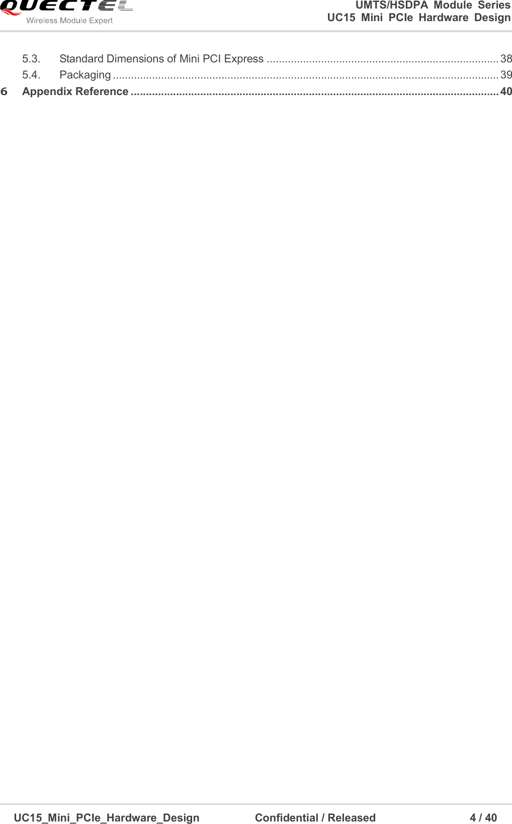
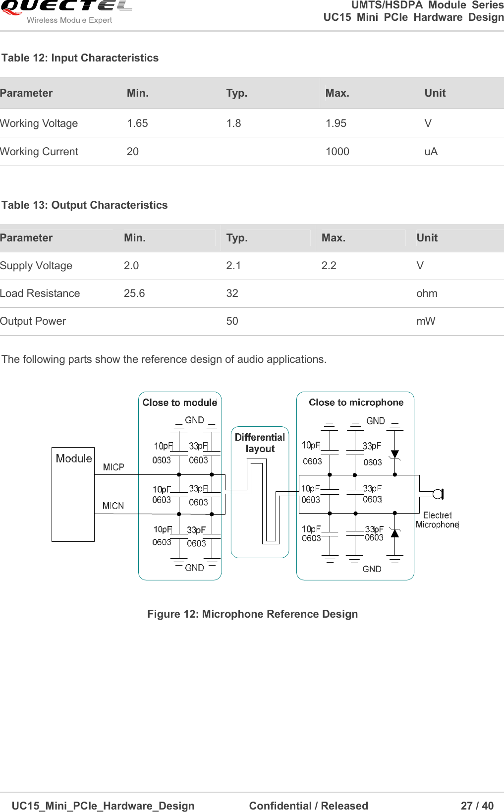
![UMTS/HSDPA Module Series UC15 Mini PCIe Hardware Design UC15_Mini_PCIe_Hardware_Design Confidential / Released 24 / 40 There are three preconditions when enabling UC15 Mini PCIe to enter the sleep mode: 1. Execute AT command AT+QSCLK=1 to enable the sleep mode. Refer to document [2]. 2. UART_DTR pin should be kept in high level (pull-up internally). 3. USB interface on Mini PCIe must be connected with your USB interface, and guarantee USB devices are in the suspended state. 3.7. Audio Interface 3.7.1. Digital Audio Interface UC15 Mini PCIe Telematics version provides one Pulse Code Modulation (PCM) digital audio interface, which supports the following modes. Short sync mode (works as both master and slave) Long sync mode (works as master only) When module works in the short sync mode, PCM_CLK=2048kHz and PCM_SYNC=8kHz. The data is sampled on the falling edge of the PCM_CLK and transmitted on the rising edge, and the PCM_SYNC falling edge represents the MSB. When module works in the long sync mode, PCM_CLK=128kHz and PCM_SYNC=8kHz. The data is sampled on the falling edge of the PCM_CLK and transmitted on the rising edge, and the PCM_SYNC rising edge represents the MSB. The following figures show timing relationship of these two modes. Figure 9: Short Sync Mode Timing NOTES](https://usermanual.wiki/Quectel-Wireless-Solutions/201404UC15M/User-Guide-2455653-Page-25.png)
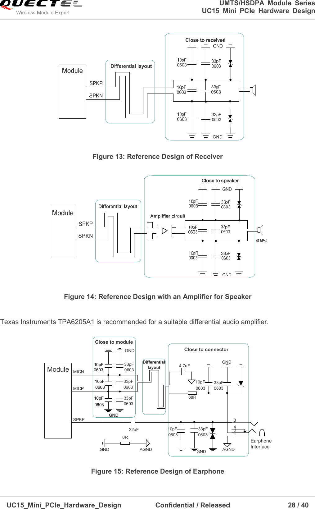
![UMTS/HSDPA Module Series UC15 Mini PCIe Hardware Design UC15_Mini_PCIe_Hardware_Design Confidential / Released 25 / 40 Figure 10: Long Sync Mode Timing I2C interface can be used to work with PCM interface for the audio codec design. The following table shows the pin definition of PCM and I2C interfaces. Table 10: Pin Definition of PCM and I2C Interface Module firmware has integrated the configuration on NAU8814 application with I2C interface, and works in short sync mode by default. You can enable this configuration with command AT+QDAI=2, and AT+QAUDPATH=2 will configure the audio channel to PCM interface, AT+QAUDPATH=0 configures the audio channel to analog audio interface. Refer to document [2] for details. Pin No. Pin Name I/O Description Power Domain 30 I2C_SCL DO I2C clock signal Require external pull-up to 2.6V. 32 I2C_SDA IO I2C data signal Require external pull-up to 2.6V. 45 PCM_CLK IO PCM clock signal 2.6V 47 PCM_DOUT DO PCM data output 2.6V 49 PCM_DIN DI PCM data input 2.6V 51 PCM_SYNC IO PCM frame sync signal 2.6V](https://usermanual.wiki/Quectel-Wireless-Solutions/201404UC15M/User-Guide-2455653-Page-26.png)
![UMTS/HSDPA Module Series UC15 Mini PCIe Hardware Design UC15_Mini_PCIe_Hardware_Design Confidential / Released 29 / 40 You can use AT+QMIC to adjust the input gain level of microphone, use AT+CLVL to adjust the output gain level of receiver and speaker. AT+QSIDET is to set the side-tone gain level. For more details, please refer to document [2]. The 33pF capacitors and 10pF capacitors are applied for filtering out 850/900/1800/1900MHz RF interference. However, the self-resonant frequency point of capacitor largely depends on the material and production technique. Therefore, you should depend on the capacitor vendor to choose the most suitable capacitor for filtering out GSM850, EGSM900, DCS1800 and PCS1900 separately. In order to decrease radio or other signal interference, RF antenna should be kept away from audio interface and audio alignment. Power alignment and audio alignment should not be parallel, and power alignment should be far away from audio alignment. The differential audio traces should be placed according to the differential signal layout rules. 3.8. Control Signals The following table shows the pin definition of control signals. Table 14: Description of Control Signal Pins 3.8.1. W_DISABLE# Signal UC15 Mini PCIe provides W_DISABLE# signal to disable wireless communications through hardware operation. The following table shows the radio operational states of module. Please refer to document [2] for related AT commands. Table 15: Radio Operational States Pin No. Pin Name I/O Power Domain Description 20 W_DISABLE# DI 3.3V Disable wireless communications. Active low. 22 PERST# DI 3.3V Functional reset to the card. Active low pulse. 42 LED_WWAN# OC — Active-low LED signal for indicating the state of the card. W_DISABLE# AT Commands Radio Operation High Level AT+CFUN=1 Enabled](https://usermanual.wiki/Quectel-Wireless-Solutions/201404UC15M/User-Guide-2455653-Page-30.png)
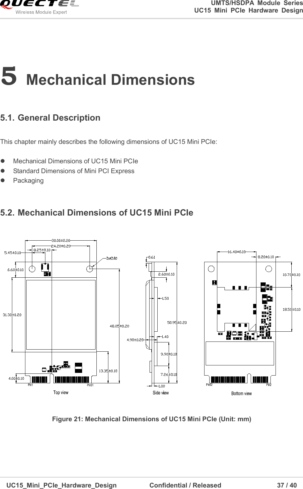
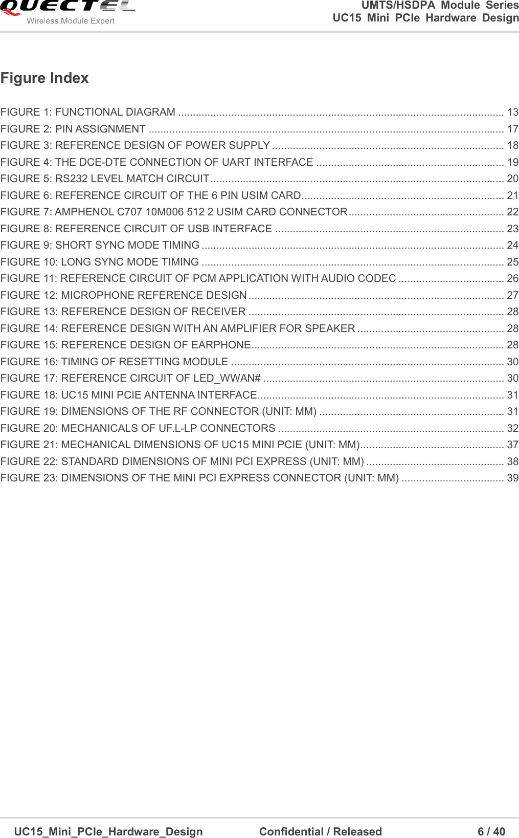
![UMTS/HSDPA Module Series UC15 Mini PCIe Hardware Design UC15_Mini_PCIe_Hardware_Design Confidential / Released 38 / 40 5.3. Standard Dimensions of Mini PCI Express The following figure shows the standard Dimensions of Mini PCI Express. Please refer to document [1] for detail A and detail B. Figure 22: Standard Dimensions of Mini PCI Express (Unit: mm) UC15 Mini PCIe adopts a standard Mini PCI Express connector which compiles with the standards listed in the document [1]. The following figure takes the Molex 679100002 as an example.](https://usermanual.wiki/Quectel-Wireless-Solutions/201404UC15M/User-Guide-2455653-Page-39.png)
![UMTS/HSPA Module UC15 Mini PCIe Hardware Design UC15_Mini_PCIe_Hardware_Design Confidential / Released 40 / 40 6 Appendix Reference Table 24: Related Documents Table 25: Terms and Abbreviations SN Document Name Remark [1] PCI Express Mini Card Electromechanical Specification Revision 1.2 Mini PCI Express Specification. [2] Quectel_UC15_AT_Commands_Manual UC15 AT Commands Manual. Abbreviation Description bps Bits Per Second CS Coding Scheme CSD Circuit Switched Data CTS Clear to Send DCE Data Communications Equipment (typically module) DL Down Link DTE Data Terminal Equipment (typically computer, external controller) DTR Data Terminal Ready EMC Electromagnetic Compatibility ESD Electrostatic Discharge GMSK Gaussian Minimum Shift Keying GSM Global System for Mobile Communications HSDPA High Speed Downlink Packet Access](https://usermanual.wiki/Quectel-Wireless-Solutions/201404UC15M/User-Guide-2455653-Page-41.png)