Quectel Wireless Solutions 201404UC15M UMTS/HSDPA module User Manual Manual
Quectel Wireless Solutions Company Limited UMTS/HSDPA module Manual
Manual

UC15 Mini PCIe
Hardware Design
UMTS/HSDPA Module Series
Rev. UC15_Mini_PCIe_Hardware_Design_V1.0
Date: 2014-07-11
www.quectel.com

UMTS/HSDPA Module Series
UC15 Mini PCIe Hardware Design
UC15_Mini_PCIe_Hardware_Design Confidential / Released 1 / 40
Our aim is to provide customers with timely and comprehensive service. For any
assistance, please contact our company headquarters:
Quectel Wireless Solutions Co., Ltd.
Office 501, Building 13, No.99, Tianzhou Road, Shanghai, China, 200233
Tel: +86 21 5108 6236
Mail: info@quectel.com
Or our local office, for more information, please visit:
http://www.quectel.com/support/salesupport.aspx
For technical support, to report documentation errors, please visit:
http://www.quectel.com/support/techsupport.aspx
GENERAL NOTES
QUECTEL OFFERS THIS INFORMATION AS A SERVICE TO ITS CUSTOMERS. THE INFORMATION
PROVIDED IS BASED UPON CUSTOMERS’ REQUIREMENTS. QUECTEL MAKES EVERY EFFORT
TO ENSURE THE QUALITY OF THE INFORMATION IT MAKES AVAILABLE. QUECTEL DOES NOT
MAKE ANY WARRANTY AS TO THE INFORMATION CONTAINED HEREIN, AND DOES NOT ACCEPT
ANY LIABILITY FOR ANY INJURY, LOSS OR DAMAGE OF ANY KIND INCURRED BY USE OF OR
RELIANCE UPON THE INFORMATION. THE INFORMATION SUPPLIED HEREIN IS SUBJECT TO
CHANGE WITHOUT PRIOR NOTICE.
COPYRIGHT
THIS INFORMATION CONTAINED HERE IS PROPRIETARY TECHNICAL INFORMATION OF
QUECTEL CO., LTD. TRANSMITTABLE, REPRODUCTION, DISSEMINATION AND EDITING OF THIS
DOCUMENT AS WELL AS UTILIZATION OF THIS CONTENTS ARE FORBIDDEN WITHOUT
PERMISSION. OFFENDERS WILL BE HELD LIABLE FOR PAYMENT OF DAMAGES. ALL RIGHTS
ARE RESERVED IN THE EVENT OF A PATENT GRANT OR REGISTRATION OF A UTILITY MODEL
OR DESIGN.
Copyright © Quectel Wireless Solutions Co., Ltd. 2014. All rights reserved.

UMTS/HSDPA Module Series
UC15 Mini PCIe Hardware Design
UC15_Mini_PCIe_Hardware_Design Confidential / Released 2 / 40
About the Document
History
Revision Date Author Description
1.0 2014-07-11 Mountain ZHOU Initial

UMTS/HSDPA Module Series
UC15 Mini PCIe Hardware Design
UC15_Mini_PCIe_Hardware_Design Confidential / Released 3 / 40
Contents
About the Document ................................................................................................................................... 2
Contents ....................................................................................................................................................... 3
Table Index ................................................................................................................................................... 5
Figure Index ................................................................................................................................................. 6
1 Introduction .......................................................................................................................................... 7
1.1. Safety Information...................................................................................................................... 7
2 Product Concept .................................................................................................................................. 9
2.1. General Description ................................................................................................................... 9
2.2. Description of Product Version .................................................................................................. 9
2.3. Directives and Standards ........................................................................................................ 10
2.3.1. FCC Statement ............................................................................................................... 10
2.3.2. FCC Radiation Exposure Statement .............................................................................. 10
2.4. Key Features ........................................................................................................................... 10
2.5. Functional Diagram ................................................................................................................. 12
3 Application Interface ......................................................................................................................... 14
3.1. General Description ................................................................................................................. 14
3.2. UC15 Mini PCIe Interface ........................................................................................................ 14
3.2.1. Definition of Interface ..................................................................................................... 14
3.2.2. Pin Assignment .............................................................................................................. 17
3.3. Power Supply ........................................................................................................................... 18
3.4. UART Interface ........................................................................................................................ 18
3.5. USIM Card Interface ................................................................................................................ 20
3.6. USB Interface .......................................................................................................................... 23
3.7. Audio Interface ......................................................................................................................... 24
3.7.1. Digital Audio Interface .................................................................................................... 24
3.7.2. Analog Audio Interface ................................................................................................... 26
3.8. Control Signals ........................................................................................................................ 29
3.8.1. W_DISABLE# Signal ...................................................................................................... 29
3.8.2. PERST# Signal .............................................................................................................. 30
3.8.3. LED_WWAN# Signal ..................................................................................................... 30
3.9. Antenna Interface .................................................................................................................... 31
4 Electrical and Radio Characteristics ............................................................................................... 33
4.1. General Description ................................................................................................................. 33
4.2. Power Supply Requirements ................................................................................................... 33
4.3. IO Requirements ...................................................................................................................... 33
4.4. Current Consumption .............................................................................................................. 34
4.5. RF Characteristics ................................................................................................................... 35
4.6. ESD Characteristics ................................................................................................................ 36
5 Mechanical Dimensions .................................................................................................................... 37
5.1. General Description ................................................................................................................. 37
5.2. Mechanical Dimensions of UC15 Mini PCIe ........................................................................... 37

UMTS/HSDPA Module Series
UC15 Mini PCIe Hardware Design
UC15_Mini_PCIe_Hardware_Design Confidential / Released 4 / 40
5.3. Standard Dimensions of Mini PCI Express ............................................................................. 38
5.4. Packaging ................................................................................................................................ 39
6 Appendix Reference .......................................................................................................................... 40

UMTS/HSDPA Module Series
UC15 Mini PCIe Hardware Design
UC15_Mini_PCIe_Hardware_Design Confidential / Released 5 / 40
Table Index
TABLE 1: PRODUCT VERSION OF UC15 MINI PCIE ....................................................................................... 9
TABLE 2: KEY FEATURES OF UC15 MINI PCIE .............................................................................................. 11
TABLE 3: DEFINITION OF IO PARAMETERS .................................................................................................. 14
TABLE 4: DESCRIPTION OF PIN ..................................................................................................................... 15
TABLE 5: VCC_3V3 AND GND PINS ................................................................................................................ 18
TABLE 6: PIN DEFINITION OF THE UART INTERFACE ................................................................................. 19
TABLE 7: PIN DEFINITION OF THE USIM CARD INTERFACE ...................................................................... 20
TABLE 8: PIN DESCRIPTION OF AMPHENOL USIM CARD CONNECTOR .................................................. 22
TABLE 9: USB PIN DESCRIPTION .................................................................................................................. 23
TABLE 10: PIN DEFINITION OF PCM AND I2C INTERFACE .......................................................................... 25
TABLE 11: PIN DEFINITION OF ANALOG AUDIO INTERFACE ...................................................................... 26
TABLE 12: INPUT CHARACTERISTICS ........................................................................................................... 27
TABLE 13: OUTPUT CHARACTERISTICS ....................................................................................................... 27
TABLE 14: DESCRIPTION OF CONTROL SIGNAL PINS ................................................................................ 29
TABLE 15: RADIO OPERATIONAL STATES .................................................................................................... 29
TABLE 16: INDICATION OF NETWORK STATUS ............................................................................................ 31
TABLE 17: ANTENNA REQUIREMENTS .......................................................................................................... 32
TABLE 18: POWER SUPPLY REQUIREMENTS .............................................................................................. 33
TABLE 19: IO REQUIREMENTS ....................................................................................................................... 34
TABLE 20: CURRENT CONSUMPTION ........................................................................................................... 34
TABLE 21: OUTPUT POWER OF CONDUCTED RF ....................................................................................... 35
TABLE 22: RECEIVING SENSITIVITY OF CONDUCTED RF .......................................................................... 35
TABLE 23: ESD CHARACTERISTICS .............................................................................................................. 36
TABLE 24: RELATED DOCUMENTS ................................................................................................................ 40
TABLE 25: TERMS AND ABBREVIATIONS ...................................................................................................... 40

UMTS/HSDPA Module Series
UC15 Mini PCIe Hardware Design
UC15_Mini_PCIe_Hardware_Design Confidential / Released 6 / 40
Figure Index
FIGURE 1: FUNCTIONAL DIAGRAM ............................................................................................................... 13
FIGURE 2: PIN ASSIGNMENT ......................................................................................................................... 17
FIGURE 3: REFERENCE DESIGN OF POWER SUPPLY ............................................................................... 18
FIGURE 4: THE DCE-DTE CONNECTION OF UART INTERFACE ................................................................ 19
FIGURE 5: RS232 LEVEL MATCH CIRCUIT .................................................................................................... 20
FIGURE 6: REFERENCE CIRCUIT OF THE 6 PIN USIM CARD ..................................................................... 21
FIGURE 7: AMPHENOL C707 10M006 512 2 USIM CARD CONNECTOR ..................................................... 22
FIGURE 8: REFERENCE CIRCUIT OF USB INTERFACE .............................................................................. 23
FIGURE 9: SHORT SYNC MODE TIMING ....................................................................................................... 24
FIGURE 10: LONG SYNC MODE TIMING ....................................................................................................... 25
FIGURE 11: REFERENCE CIRCUIT OF PCM APPLICATION WITH AUDIO CODEC .................................... 26
FIGURE 12: MICROPHONE REFERENCE DESIGN ....................................................................................... 27
FIGURE 13: REFERENCE DESIGN OF RECEIVER ....................................................................................... 28
FIGURE 14: REFERENCE DESIGN WITH AN AMPLIFIER FOR SPEAKER .................................................. 28
FIGURE 15: REFERENCE DESIGN OF EARPHONE ...................................................................................... 28
FIGURE 16: TIMING OF RESETTING MODULE ............................................................................................. 30
FIGURE 17: REFERENCE CIRCUIT OF LED_WWAN# .................................................................................. 30
FIGURE 18: UC15 MINI PCIE ANTENNA INTERFACE .................................................................................... 31
FIGURE 19: DIMENSIONS OF THE RF CONNECTOR (UNIT: MM) ............................................................... 31
FIGURE 20: MECHANICALS OF UF.L-LP CONNECTORS ............................................................................. 32
FIGURE 21: MECHANICAL DIMENSIONS OF UC15 MINI PCIE (UNIT: MM) ................................................. 37
FIGURE 22: STANDARD DIMENSIONS OF MINI PCI EXPRESS (UNIT: MM) ............................................... 38
FIGURE 23: DIMENSIONS OF THE MINI PCI EXPRESS CONNECTOR (UNIT: MM) ................................... 39

UMTS/HSDPA Module Series
UC15 Mini PCIe Hardware Design
UC15_Mini_PCIe_Hardware_Design Confidential / Released 7 / 40
1 Introduction
This document defines UC15 Mini PCIe module and describes its hardware interfaces which are
connected with your application and air interfaces.
This document can help you to quickly understand the interface specifications, electrical and mechanical
details and related product information of the UC15 Mini PCIe module. Associated with application notes
and user guide of UC15 Mini PCIe module, you can use the module to design and set up mobile
applications easily.
1.1. Safety Information
The following safety precautions must be observed during all phases of the operation, such as usage,
service or repair of any cellular terminal or mobile incorporating UC15 Mini PCIe module. Manufacturers
of the cellular terminal should send the following safety information to users and operating personnel and
to incorporate these guidelines into all manuals supplied with the product. If not so, Quectel does not take
on any liability for customer failure to comply with these precautions.
Full attention must be given to driving at all times in order to reduce the risk of an
accident. Using a mobile while driving (even with a handsfree kit) cause distraction
and can lead to an accident. You must comply with laws and regulations restricting
the use of wireless devices while driving.
Switch off the cellular terminal or mobile before boarding an aircraft. Make sure it
switched off. The operation of wireless appliances in an aircraft is forbidden to
prevent interference with communication systems. Consult the airline staff about
the use of wireless devices on boarding the aircraft, if your device offers a Airplane
Mode which must be enabled prior to boarding an aircraft.
Switch off your wireless device when in hospitals or clinics or other health care
facilities. These requests are desinged to prevent possible interference with
sentitive medical equipment.
UMTS/HSDPA Module Series
UC15 Mini PCIe Hardware Design
UC15_Mini_PCIe_Hardware_Design Confidential / Released 8 / 40
Cellular terminals or mobiles operate over radio frequency signal and cellular
network and cannot be guaranteed to connect in all conditions, for example no
mobile fee or an invalid SIM card. While you are in this condition and need
emergent help, please remember using emergency call. In order to make or
receive call, the cellular terminal or mobile must be switched on and in a service
area with adequate cellular signal strength.
Your cellular terminal or mobile contains a transmitter and receiver. When it is ON,
it receives and transmits radio frequency energy. RF interference can occur if it is
used close to TV set, radio, computer or other electric equipment.
In locations with potencially explosive atmospheres, obey all posted signs to turn
off wireless devices such as your phone or other cellular terminals. Areas with
potencially exposive atmospheres including fuelling areas, below decks on boats,
fuel or chemical transfer or storage facilities, areas where the air contains
chemicals or particles such as grain, dust or metal powders.

UMTS/HSDPA Module Series
UC15 Mini PCIe Hardware Design
UC15_Mini_PCIe_Hardware_Design Confidential / Released 9 / 40
2 Product Concept
2.1. General Description
UC15 Mini PCIe module is a cost effective UMTS/HSDPA module featuring a maximum data rate of
3.6Mbps downlink and 384kbps uplink, according to PCI Express Mini Card 1.2 standard, supports
embedded operating system such as WinCE, Linux and Android etc.
UC15 Mini PCIe module can be applied in the following fields:
PDAs and Laptop Computer
Remote Monitor System
Vehicle System
Wireless POS System
Intelligent Meter Reading System
Wireless Router and Switch
Other Wireless Terminal Device
This chapter generally introduces the following aspects of UC15 Mini PCIe module:
Product Version
Key Features
Functional Diagram
2.2. Description of Product Version
The following table shows the product version of UC15 Mini PCIe module.
Table 1: Product Version of UC15 Mini PCIe
Product Version Description
Telematics Support voice and data.
Data Only Support data only.

UMTS/HSDPA Module Series
UC15 Mini PCIe Hardware Design
UC15_Mini_PCIe_Hardware_Design Confidential / Released 10 / 40
2.3. Directives and Standards
The UC15 Mini PCIe module is designed to comply with the FCC statements.FCC ID:XMR201404UC15M
If the FCC ID of the module cannot be seen by the user in the final installation, the host device must show
the statement: “Contains FCC ID: XMR201404UC15M” in a visible and permanent location”
2.3.1. FCC Statement
1. This device complies with Part 15 of the FCC rules. Operation is subject to the following conditions:
a) This device may not cause harmful interference.
b) This device must accept any interference received, including interference that may cause undesired
operation.
2. Changes or modifications not expressly approved by the party responsible for compliance could avoid
the user’s authority to operate the equipment.
2.3.2. FCC Radiation Exposure Statement
This equipment complies with FCC radiation exposure limits set forth for an uncontrolled environment.
This equipment should be installed and operated with minimum distance 20cm between the radiator and
your body as well as kept minimum 20cm from radio antenna depending on the Mobile status of this
module usage. This module should NOT be installed and operating simultaneously with other radio.
The manual of the host system, which uses UC15 Mini PCIe, must include RF exposure warning
statement to advice user should keep minimum 20cm from the radio antenna of UC15 Mini PCIe module
depending on the mobile status.
Note: If a portable device (such as PDA) uses UC15 Mini PCIe module, the device needs to do
permissive change and SAR testing.
The following list of antenna is indicating the maximum permissible antenna gain.
Part Number
Frequency
Range (MHz)
Peak Gain
(XZ-V)
Average Gain
(XZ-V) VSWR Impedance
3R007A
GSM850:824~849
PCS1900:1850~1990
UMTS1900:1850~1990
UMTS850:824-894
1 dBi typ. 1 dBi typ. 3 max 50Ω
2.4. Key Features
The following table describes the detailed features of UC15 Mini PCIe module.

UMTS/HSDPA Module Series
UC15 Mini PCIe Hardware Design
UC15_Mini_PCIe_Hardware_Design Confidential / Released 11 / 40
Table 2: Key Features of UC15 Mini PCIe
Feature Details
Function Interface PCI Express Mini Card 1.2 Standard Interface
Power Supply Supply voltage: 3.0~3.6V
Typical supply voltage: 3.3V
Frequency Bands GSM850/900/1800/1900, UMTS850/1900
Transmission Data
HSDPA R5: Max 3.6Mbps (DL)
UMTS R99: Max 384kbps (DL)/Max 384kbps (UL)
EDGE: Max 236.8kbps (DL only)
GPRS: Max 85.6kbps (DL)/Max 85.6kbps (UL)
CSD: 64kbps
Transmitting Power
Class 4 (33dBm±2dB) for GSM850 and EGSM900
Class 1 (30dBm±2dB) for DCS1800 and PCS1900
Class E2 (27dBm±3dB) for GSM850 and EGSM900
Class E2 (26dBm+3/-4dB) for DCS1800 and PCS1900
Class 3 (24dBm+1/-3dB) for UMTS850/1900
HSDPA and WCDMA
Features
HSDPA data rate is corresponded with 3GPP R5. 3.6Mbps on downlink.
WCDMA data rate is corresponded with 3GPP R99/R4. 384kbps on
downlink and 384kbps on uplink.
Support both QPSK and 16-QAM modulation.
GSM/GPRS/EDGE
Data Features
GPRS: Support GPRS multi-slot class 12 (10 by default).
Coding scheme: CS-1, CS-2, CS-3 and CS-4.
Maximum of four Rx time slots per frame.
EDGE: Support EDGE multi-slot class 12 (12 by default).
Support GMSK for different MCS (Modulation and Coding
Scheme).
Downlink coding schemes: CS 1-4 and MCS 1-9.
CSD: CSD transmission rates: 64kbps non-transparent.
Support Unstructured Supplementary Services Data (USSD).
Internet Protocol Features
Support TCP/IP/PPP/UDP protocols.
Support the protocols PAP (Password Authentication Protocol) and
CHAP (Challenge Handshake Authentication Protocol) usually used for
PPP connections.
SMS
Text and PDU mode
Point to point MO and MT
SMS cell broadcast
SMS storage: ME by default
USIM Interface Support USIM/SIM card: 1.8V, 3.0V
UART Interface
Support seven lines on UART interface.
Support RTS and CTS hardware flow control.
Baud rate can reach up to 230400 bps, 115200 bps by default.
UMTS/HSDPA Module Series
UC15 Mini PCIe Hardware Design
UC15_Mini_PCIe_Hardware_Design Confidential / Released 12 / 40
1. “▲” means when the module works within this temperature range, RF performance might degrade.
For example, the frequency error or the phase error may increase.
2. “*” means these functions are only supported in Telematics version.
2.5. Functional Diagram
The following figure shows a block diagram of UC15 Mini PCIe and illustrates the major functional parts:
USIM/SIM card interface (1.8V/3.0V)
USB 2.0 interface
UART interface (seven lines)
Used for AT command and data transmission.
Support multiplexing function.
Analog Audio Interface*
Support one differential input and one differential output channel.
GSM: HR/FR/EFR/AMR/AMR-WB
WCDMA: AMR/AMR-WB
Echo cancellation and noise suppression
PCM Digital Audio
Interface*
Support 16-bit linear data formats.
Support long frame sync and short frame sync.
Support master and slave mode, but must be the master in long frame
sync.
USB Interface
Compliant with USB 2.0 specification (slave only), the data transfer rate
can reach up to 480 Mbps.
Used for AT command communication, data transmission, software
debug and firmware upgrade.
USB Driver: Support Windows XP, Windows Vista, Windows 7, Windows
8, WinCE 5.0/6.0, Windows Mobile 6.1/6.5, Linux 2.6 or later, Android 2.3
or later.
Antenna Interface One GSM/UMTS antenna connector.
AT Commands Compliant with 3GPP TS 27.007, 27.005 and Quectel enhanced AT
commands.
Physical Characteristics Size: 51.0 × 30.0 × 4.9mm
Weight: Approx. 9.3g
Temperature Range
Normal operation: -30°C ~ +70°C
Restricted operation: -40°C ~ -30°C and +70°C ~ +80°C▲
Storage temperature: -45°C ~ +90°C
Firmware Upgrade USB interface
RoHS All hardware components are fully compliant with EU RoHS directive.
NOTES
UMTS/HSDPA Module Series
UC15 Mini PCIe Hardware Design
UC15_Mini_PCIe_Hardware_Design Confidential / Released 13 / 40
Audio interface
I2C interface
Support LED status indication
Support disabling wireless communication function
Support hardware reset function
Support GSM/UMTS antenna interface
Mini PCI Express
Interface
Figure 1: Functional Diagram

UMTS/HSDPA Module Series
UC15 Mini PCIe Hardware Design
UC15_Mini_PCIe_Hardware_Design Confidential / Released 14 / 40
3 Application Interface
3.1. General Description
The physical connections and signal levels of UC15 Mini PCIe comply with PCI Express Mini CEM
specifications. This chapter mainly describes the definition of following interfaces and applications of
UC15 Mini PCIe.
Power supply
UART interface
USIM interface
USB interface
Audio interface
Antenna interface
Control signals (W_DISABLE#, PERST# and LED_WWAN#)
3.2. UC15 Mini PCIe Interface
3.2.1. Definition of Interface
The following tables show the pin assignments of UC15 Mini PCIe on the 52-pin application.
Table 3: Definition of IO Parameters
Type Description
AI Analog input
AO Analog output
DI Digital input
DO Digital output
IO Bidirectional input/output
OC Open collector
UMTS/HSDPA Module Series
UC15 Mini PCIe Hardware Design
UC15_Mini_PCIe_Hardware_Design Confidential / Released 15 / 40
Table 4: Description of Pin
PI Power input
PO Power output
Pin No.
Mini PCI Express
Standard Name
UC15 Mini PCIe
Name I/O Description Comment
1 WAKE# MICP* AI Audio positive input
2 3.3Vaux VCC_3V3 PI 3.3V DC supply
3 COEX1 MICN* AI Audio negative input
4 GND GND — Mini card ground
5 COEX2 SPKP* AO Audio positive output
6 1.5V NC — —
7 CLKREQ# SPKN* AO Audio negative output
8 UIM_PWR USIM_VDD PO Power source for the USIM
card
9 GND GND — Mini card ground
10 UIM_DATA USIM_DATA IO USIM data signal
11 REFCLK- UART_RX DI UART receives data Connect to
DTE’s TX.
12 UIM_CLK USIM_CLK DO USIM clock signal
13 REFCLK+ UART_TX DO UART transmits data Connect to
DTE’s RX.
14 UIM_RESET USIM_RST DO USIM reset signal
15 GND GND — Mini card ground
16 UIM_VPP RESERVED — Reserved
17 RESERVED UART_RI DO UART ring indicator
18 GND GND — Mini card ground
19 RESERVED RESERVED — Reserved
20 W_DISABLE# W_DISABLE# DI Disable wireless
communications Active low.
21 GND GND — Mini card ground

UMTS/HSDPA Module Series
UC15 Mini PCIe Hardware Design
UC15_Mini_PCIe_Hardware_Design Confidential / Released 16 / 40
22 PERST# PERST# DI Functional reset to the card Active low
pulse.
23 PERn0 UART_CTS DI UART clear to send Connect to
DTE’s RTS.
24 3.3Vaux RESERVED — Reserved
25 PERp0 UART_RTS DO UART request to send Connect to
DTE’s CTS.
26 GND GND — Mini card ground
27 GND GND — Mini card ground
28 1.5V NC — —
29 GND GND — Mini card ground
30 SMB_CLK I2C_SCL DO I2C clock signal
31 PETn0 UART_DTR DI UART data terminal ready
32 SMB_DATA I2C_SDA IO I2C data signal
33 PETp0 UART_DCD DO UART data carrier detection
34 GND GND — Mini card ground
35 GND GND — Mini card ground
36 USB_D- USB_DM IO USB differential data (-)
37 GND GND — Mini card ground
38 USB_D+ USB_DP IO USB differential data (+)
39 3.3Vaux VCC_3V3 PI 3.3V DC supply
40 GND GND — Mini Card ground
41 3.3Vaux VCC_3V3 PI 3.3V DC supply
42 LED_WWAN# LED_WWAN# OC
Active-low LED signal for
indicating the state of the
card
43 GND GND — Mini card ground
44 LED_WLAN# RESERVED — Reserved
45 RESERVED PCM_CLK* IO PCM clock signal
46 LED_WPAN# RESERVED — Reserved
47 RESERVED PCM_DOUT* DO PCM data output
UMTS/HSDPA Module Series
UC15 Mini PCIe Hardware Design
UC15_Mini_PCIe_Hardware_Design Confidential / Released 17 / 40
1. PCM and analog audio interface are only supported in Telematics version.
2. Keep all NC, reserved and unused pins unconnected.
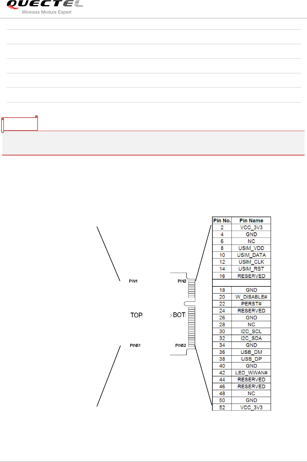
3.2.2. Pin Assignment
The following figure shows the pin assignment of UC15 Mini PCIe module. The top side contains UC15
module and antenna connectors.
Figure 2: Pin Assignment
48 1.5V NC — —
49 RESERVED PCM_DIN* DI PCM data input
50 GND GND — Mini card ground
51 RESERVED PCM_SYNC* IO PCM frame sync signal
52 3.3Vaux VCC_3V3 PI 3.3V DC supply
NOTES
UMTS/HSDPA Module Series
UC15 Mini PCIe Hardware Design
UC15_Mini_PCIe_Hardware_Design Confidential / Released 18 / 40
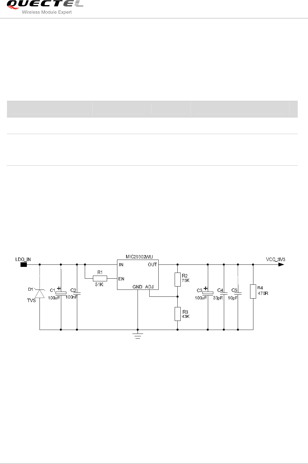
3.3. Power Supply
The following table shows the VCC_3V3 pins and ground pins.
Table 5: VCC_3V3 and GND Pins
The typical supply voltage of UC15 Mini PCIe is 3.3V. In the 2G networks, the input peak current may
reach to 2.7A during the transmitting time, therefore the power supply must be able to provide enough
current, and a bypass capacitor of no less than 100µF with low ESR should be used to prevent the
voltage from dropping.
The following figure shows a reference design of power supply. The precision of resistor R2 and R3 is 1%,
and the capacitor C3 needs a low ESR.
Figure 3: Reference Design of Power Supply
3.4. UART Interface
The following table shows the pin definition of the UART interface.
Pin No. Pin Name I/O Description
2, 39, 41, 52 VCC_3V3 PI 3.3V DC supply.
4, 9, 15, 18, 21, 26, 27, 29,
34, 35, 37, 40, 43, 50 GND — Mini card ground.
UMTS/HSDPA Module Series
UC15 Mini PCIe Hardware Design
UC15_Mini_PCIe_Hardware_Design Confidential / Released 19 / 40
Table 6: Pin Definition of the UART Interface
The UART interface supports 300, 600, 1200, 4800, 9600, 19200, 38400, 57600, 115200 and 230400bps
baud rate. The default is 115200bps. Autobauding is not supported. This interface can be used for data
transmission and AT communication.
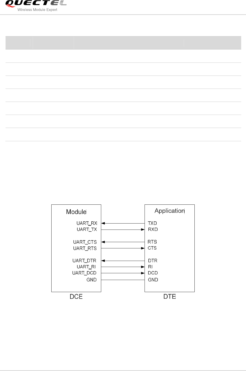
UC15 Mini PCIe is designed as the DCE, and the DCE-DTE connection of UART interface is shown as
below.
Figure 4: The DCE-DTE Connection of UART Interface
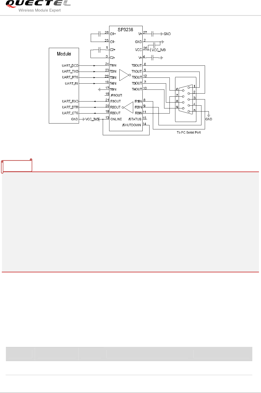
The following figure is an example of connection between UC15 Mini PCIe and PC. Since the UART
interface does not support the RS-232 level, RS-232 level translator IC must be inserted between module
and PC. The following figure shows the reference design of RS232 level match circuit.
Pin No. Pin Name I/O Description
Power Domain
11 UART_RX DI
UART receives data 3.3V
13 UART_TX
DO
UART transmits data 3.3V
17 UART_RI
DO
UART ring indicator 3.3V
23 UART_CTS DI
UART clear to send 3.3V
25 UART_RTS DO
UART request to send 3.3V
31 UART_DTR DI UART data terminal ready 3.3V
33 UART_DCD DO UART data carrier detection 3.3V
UMTS/HSDPA Module Series
UC15 Mini PCIe Hardware Design
UC15_Mini_PCIe_Hardware_Design Confidential / Released 20 / 40
Figure 5: RS232 Level Match Circuit
1. The hardware flow control is disabled by default. AT command AT+IFC=2,2 is used to enable the
hardware flow control. AT command AT+IFC=0,0 is used to disable the hardware flow control. For
more details, please refer to document [2].
2. AT command AT+IPR is used to set the baud rate of the UART. Please refer to document [2] for
details.
3. UART_DTR supports sleep control function. Driving it to low level will wake up the module, and it can
be disabled by command AT+QCFG="pwrsavedtr",0. Meanwhile, the rising edge on UART_DTR
will let the module exit from data mode. Refer to document [2] of command AT&D for details.
4. UART_DCD is used as data transferring indication. You can refer to document [2] for details of
AT&C command. This pin can also be used as AP_READY function, which can detect the host sleep
state to avoid the URC loss during the time when the host is waking up from the sleep state. For
details about AP_READY, please contact Quectel technical support.
3.5. USIM Card Interface
The following table shows the pin definition of the USIM card interface.
Table 7: Pin Definition of the USIM Card Interface
Pin No. Pin Name I/O Description
Power Domain
8 USIM_VDD
PO
Power for the USIM/SIM card. 1.8V/3.0V
NOTES
UMTS/HSDPA Module Series
UC15 Mini PCIe Hardware Design
UC15_Mini_PCIe_Hardware_Design Confidential / Released 21 / 40
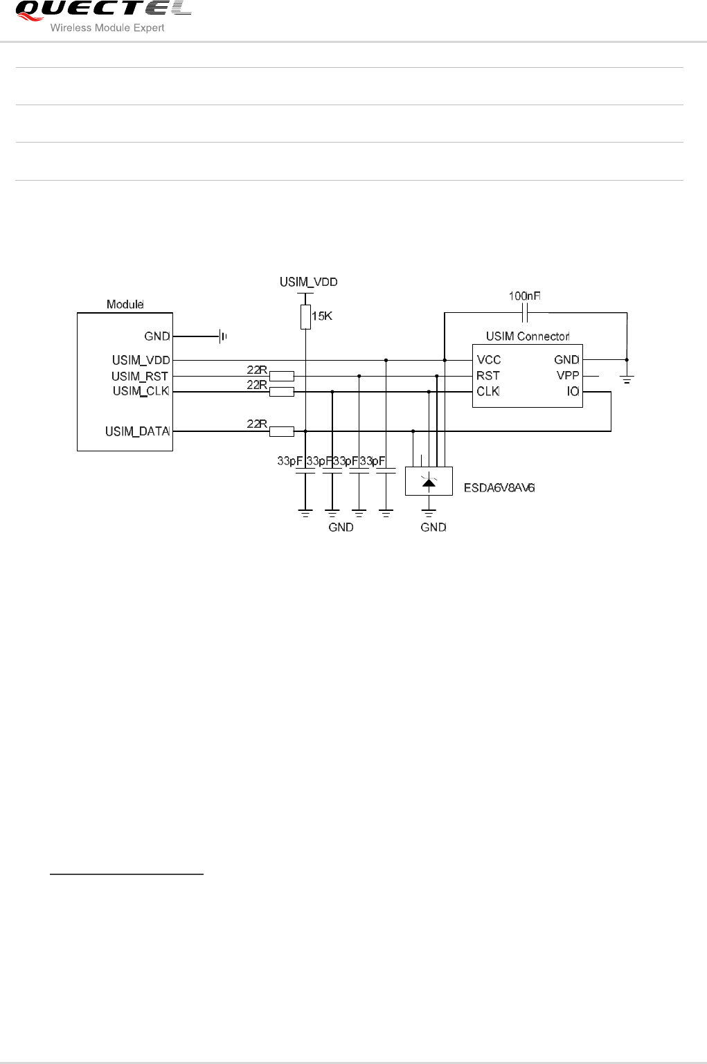
UC15 Mini PCIe supports 1.8V and 3.0V USIM cards. The following figure shows the reference design of
the 6-pin USIM card.
Figure 6: Reference Circuit of the 6 Pin USIM Card
In order to enhance the reliability and availability of the USIM card in your application, please follow the
criteria below in the USIM circuit design:
Keep layout of USIM card as close to the module as possible. Assure the length of the trace as less
than 200mm as possible.
Keep USIM card signal away from RF and power supply alignment.
The decouple capacitor of USIM_VDD should be less than 1uF and must be close to USIM
connector.
To avoid cross-talk between USIM_DATA and USIM_CLK, keep them away from each other and
shield them with surrounding ground.
In order to offer good ESD protection, it is recommended to add TVS such as WILL
(http://www.willsemi.com) ESDA6V8AV6. The 22Ω resistors should be added in series between the
module and USIM card so as to suppress the EMI spurious transmission and enhance the ESD
protection. The 33pF capacitors are used for filtering interference of EGSM900. Please note that the
USIM peripheral circuit should be close to the USIM connector.
The pull-up resistor on USIM_DATA line can improve anti-jamming capability when long layout trace
and sensitive occasion are applied.
10 USIM_DATA IO USIM/SIM data signal. 1.8V/3.0V
12 USIM_CLK DO USIM/SIM clock signal. 1.8V/3.0V
14 USIM_RST
DO
USIM/SIM reset signal. 1.8V/3.0V
UMTS/HSDPA Module Series
UC15 Mini PCIe Hardware Design
UC15_Mini_PCIe_Hardware_Design Confidential / Released 22 / 40
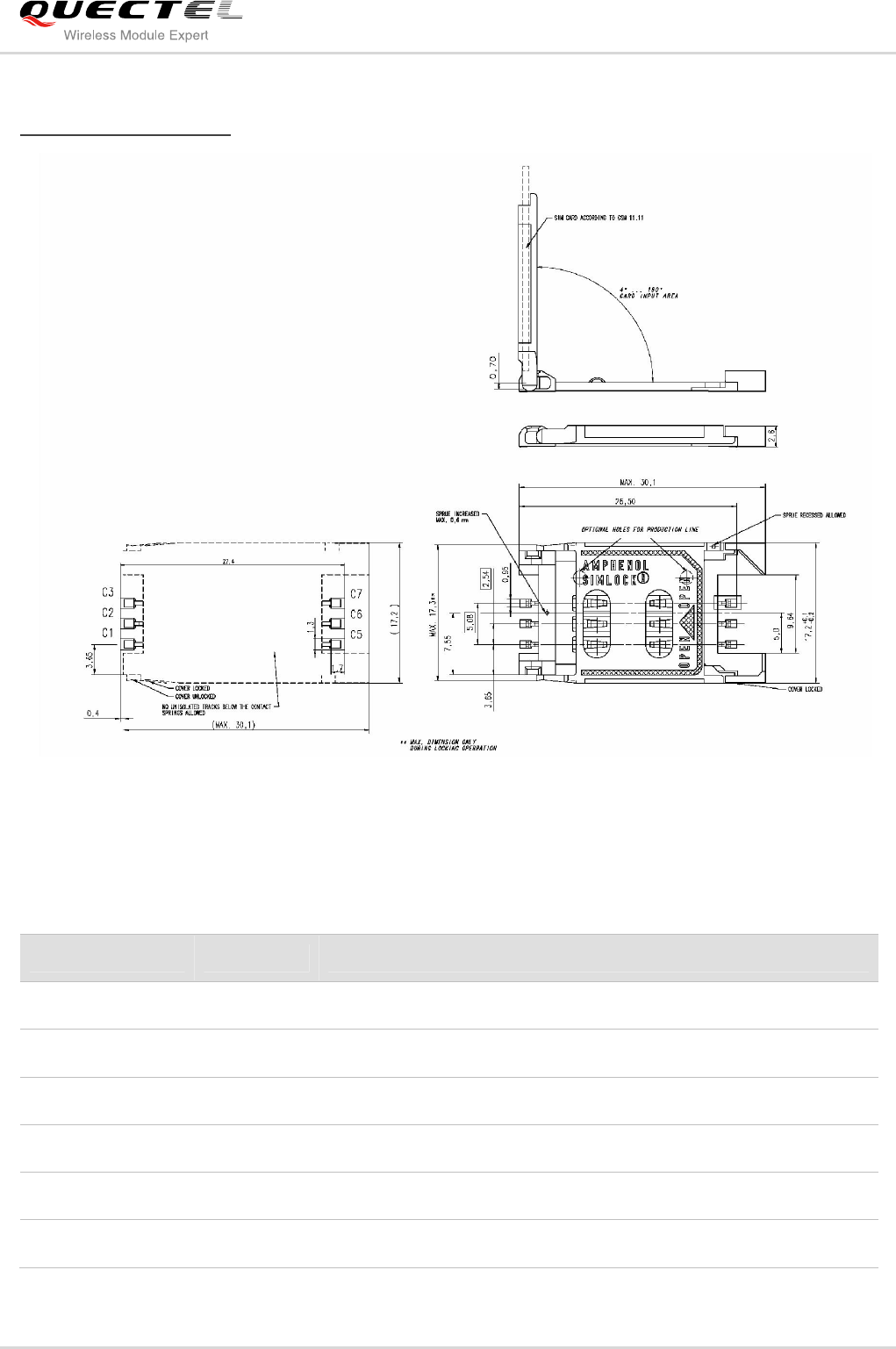
For 6-pin USIM connector, it is recommended to use Amphenol C707 10M006 512 2. Please visit
http://www.amphenol.com for more information.
Figure 7: Amphenol C707 10M006 512 2 USIM Card Connector
Table 8: Pin Description of Amphenol USIM Card Connector
Name Pin Function
VDD C1 USIM card power supply
RST C2 USIM card reset
CLK C3 USIM card clock
GND C5 Ground
VPP C6 Not connected
DATA I/O C7 USIM card data
UMTS/HSDPA Module Series
UC15 Mini PCIe Hardware Design
UC15_Mini_PCIe_Hardware_Design Confidential / Released 23 / 40
3.6. USB Interface
The following table shows the pin definition of USB interface.
Table 9: USB Pin Description
UC15 Mini PCIe is compliant with USB 2.0 specification. It can only be used as a slave device. Meanwhile,
it supports high speed (480 Mbps), full speed (12 Mbps) and low speed (1.5 Mbps) mode. The USB
interface can be used for AT command, data transmission, software debug and firmware upgrade. The
following figure shows the reference circuit of USB interface.
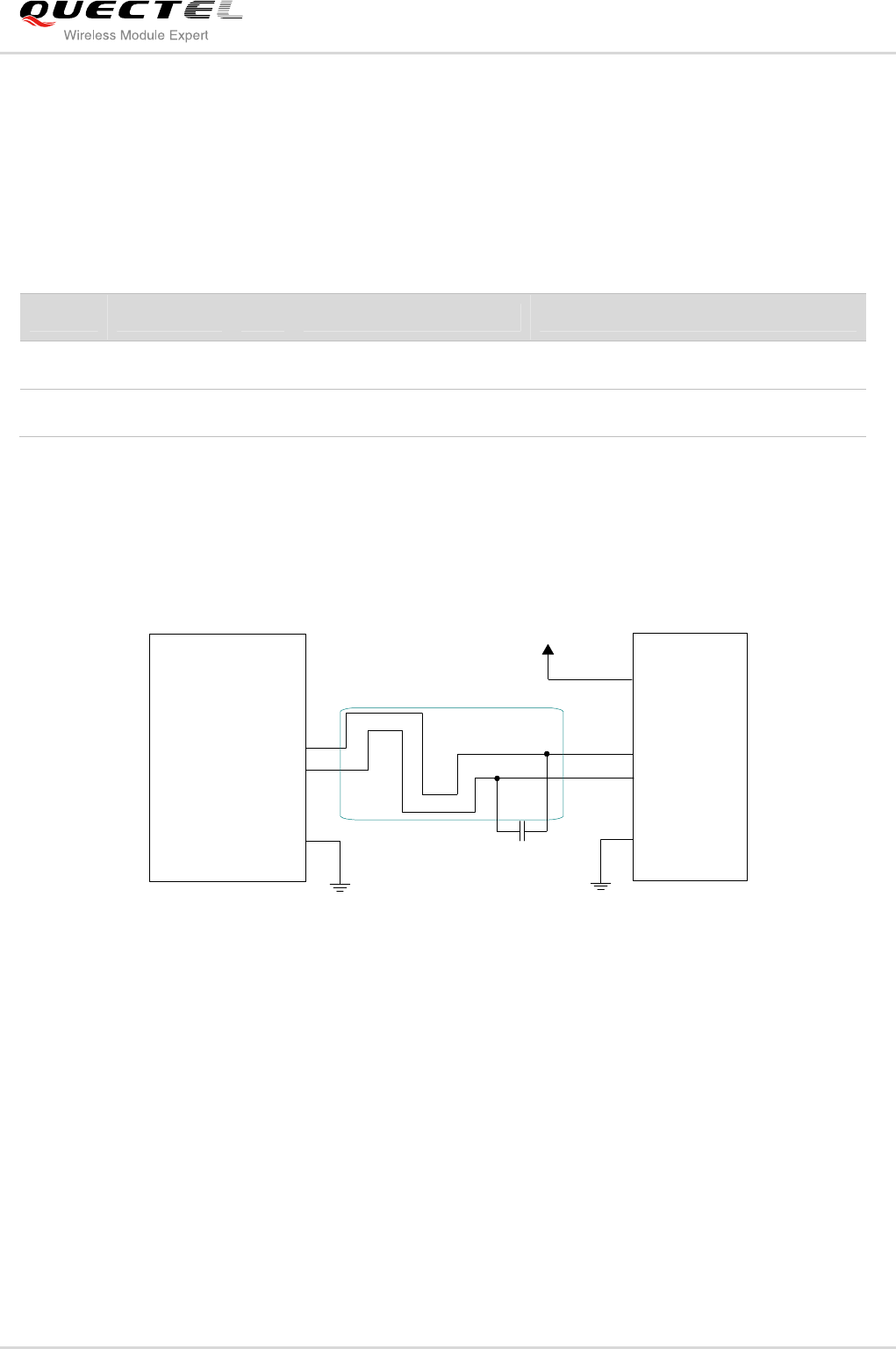
Module
USB_ DP
USB_DM
GND
MCU
Differential layout
USB_DP
USB_DM
GND
NM_2pF
VCC_MCU
VCC
Figure 8: Reference Circuit of USB Interface
To ensure the USB interface design corresponds with the USB 2.0 specification, please comply with the
following principles.
It is important to route the USB signal traces as differential pairs with total grounding. The impedance
of USB differential trace is 90ohm.
Do not route signal traces under crystals, oscillators, magnetic devices and RF signal traces. It is
important to route the USB differential traces in inner-layer with ground shielding, and not only upper
and lower layer but also right and left side should be shielded.
If you use the USB connector, you should install the ESD components as close to the USB connector
as possible. Pay attention to the influence of junction capacitance of ESD component on USB data
lines. Typically, the capacitance value should be less than 2pF (e.g.ESD9L5.0ST5G).
Pin No.
Pin Name I/O Description Comment
36 USB_DM IO USB differential data (-). Require differential impedance of 90Ω.
38 USB_DP IO USB differential data (+). Require differential impedance of 90Ω.
UMTS/HSDPA Module Series
UC15 Mini PCIe Hardware Design
UC15_Mini_PCIe_Hardware_Design Confidential / Released 24 / 40
There are three preconditions when enabling UC15 Mini PCIe to enter the sleep mode:
1. Execute AT command AT+QSCLK=1 to enable the sleep mode. Refer to document [2].
2. UART_DTR pin should be kept in high level (pull-up internally).
3. USB interface on Mini PCIe must be connected with your USB interface, and guarantee USB devices
are in the suspended state.
3.7. Audio Interface
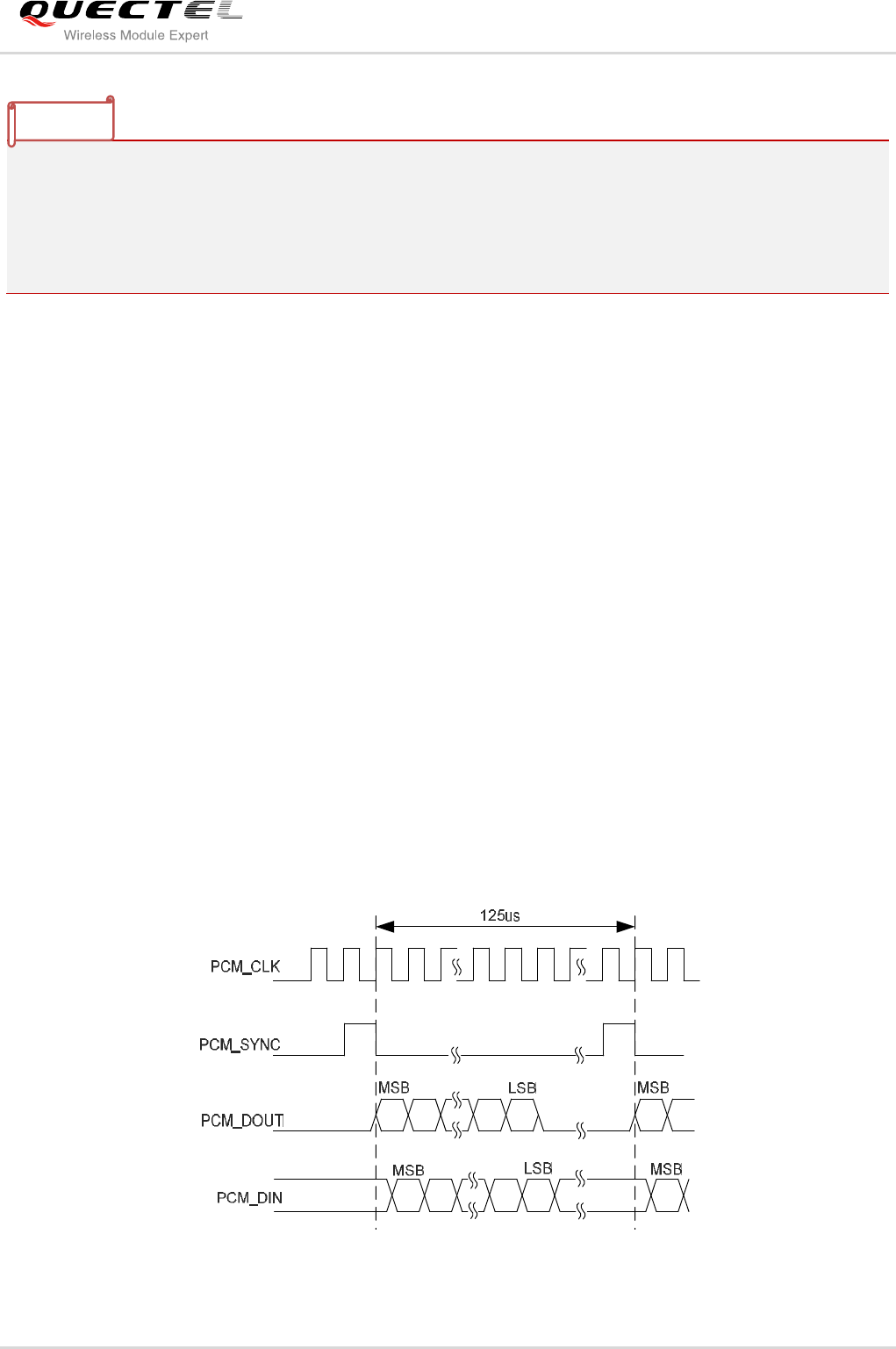
3.7.1. Digital Audio Interface
UC15 Mini PCIe Telematics version provides one Pulse Code Modulation (PCM) digital audio interface,
which supports the following modes.
Short sync mode (works as both master and slave)
Long sync mode (works as master only)
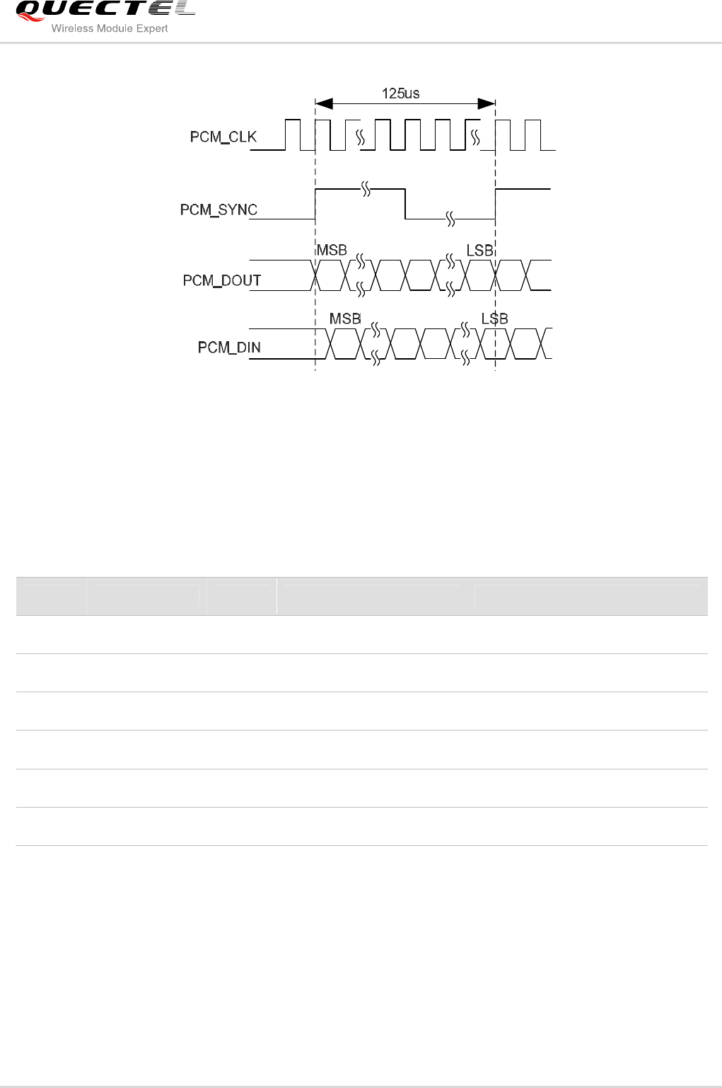
When module works in the short sync mode, PCM_CLK=2048kHz and PCM_SYNC=8kHz. The data is
sampled on the falling edge of the PCM_CLK and transmitted on the rising edge, and the PCM_SYNC
falling edge represents the MSB.
When module works in the long sync mode, PCM_CLK=128kHz and PCM_SYNC=8kHz. The data is
sampled on the falling edge of the PCM_CLK and transmitted on the rising edge, and the PCM_SYNC
rising edge represents the MSB.
The following figures show timing relationship of these two modes.
Figure 9: Short Sync Mode Timing
NOTES
UMTS/HSDPA Module Series
UC15 Mini PCIe Hardware Design
UC15_Mini_PCIe_Hardware_Design Confidential / Released 25 / 40
Figure 10: Long Sync Mode Timing
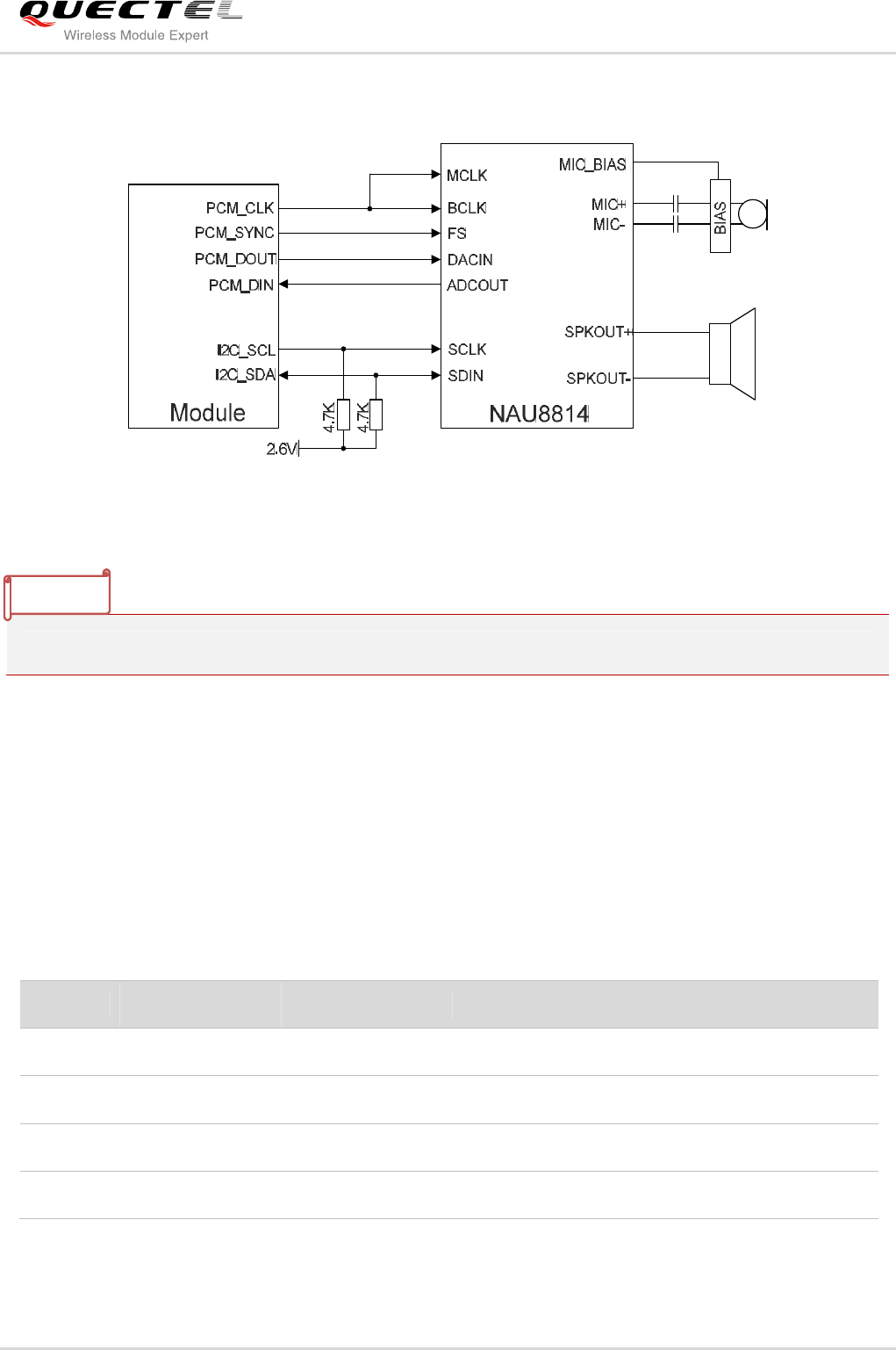
I2C interface can be used to work with PCM interface for the audio codec design. The following table
shows the pin definition of PCM and I2C interfaces.
Table 10: Pin Definition of PCM and I2C Interface
Module firmware has integrated the configuration on NAU8814 application with I2C interface, and works
in short sync mode by default. You can enable this configuration with command AT+QDAI=2, and
AT+QAUDPATH=2 will configure the audio channel to PCM interface, AT+QAUDPATH=0 configures the
audio channel to analog audio interface. Refer to document [2] for details.
Pin No.
Pin Name I/O Description Power Domain
30 I2C_SCL DO I2C clock signal Require external pull-up to 2.6V.
32 I2C_SDA IO I2C data signal Require external pull-up to 2.6V.
45 PCM_CLK IO PCM clock signal 2.6V
47 PCM_DOUT DO PCM data output 2.6V
49 PCM_DIN DI PCM data input 2.6V
51 PCM_SYNC IO PCM frame sync signal 2.6V
UMTS/HSDPA Module Series
UC15 Mini PCIe Hardware Design
UC15_Mini_PCIe_Hardware_Design Confidential / Released 26 / 40
The following figure shows the reference design of PCM interface with external codec IC.
Figure 11: Reference Circuit of PCM Application with Audio Codec
It is recommended to reserve RC (R=22Ω, C=22pF) circuit on the PCM lines, especially for PCM_CLK.
3.7.2. Analog Audio Interface
UC15 Mini PCIe Telematics version supports one differential input and output analog audio interface, and
this interface works as the default audio channel. The following tables show the pin definition and
characteristics of analog audio interface.
Table 11: Pin Definition of Analog Audio Interface
Pin No. Pin Name I/O Description
1 MICP AI Audio positive input.
3 MICN AI Audio negative input.
5 SPKP AO Audio positive output.
7 SPKN AO Audio negative output.
NOTE
UMTS/HSDPA Module Series
UC15 Mini PCIe Hardware Design
UC15_Mini_PCIe_Hardware_Design Confidential / Released 27 / 40
Table 12: Input Characteristics
Table 13: Output Characteristics
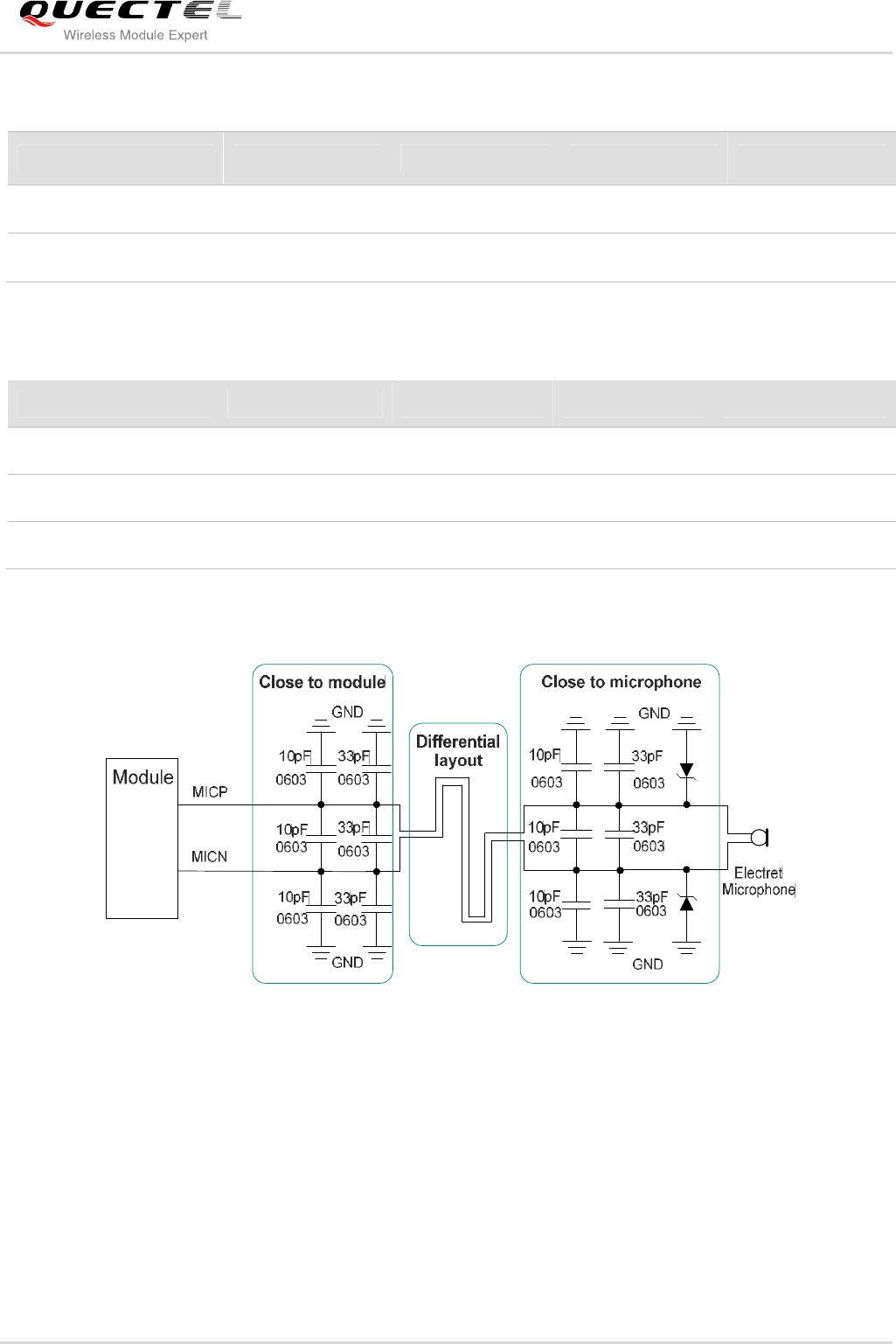
The following parts show the reference design of audio applications.
Figure 12: Microphone Reference Design
Parameter Min. Typ. Max. Unit
Working Voltage 1.65 1.8 1.95 V
Working Current 20 1000 uA
Parameter Min. Typ. Max. Unit
Supply Voltage 2.0 2.1 2.2 V
Load Resistance 25.6 32 ohm
Output Power 50 mW
UMTS/HSDPA Module Series
UC15 Mini PCIe Hardware Design
UC15_Mini_PCIe_Hardware_Design Confidential / Released 28 / 40
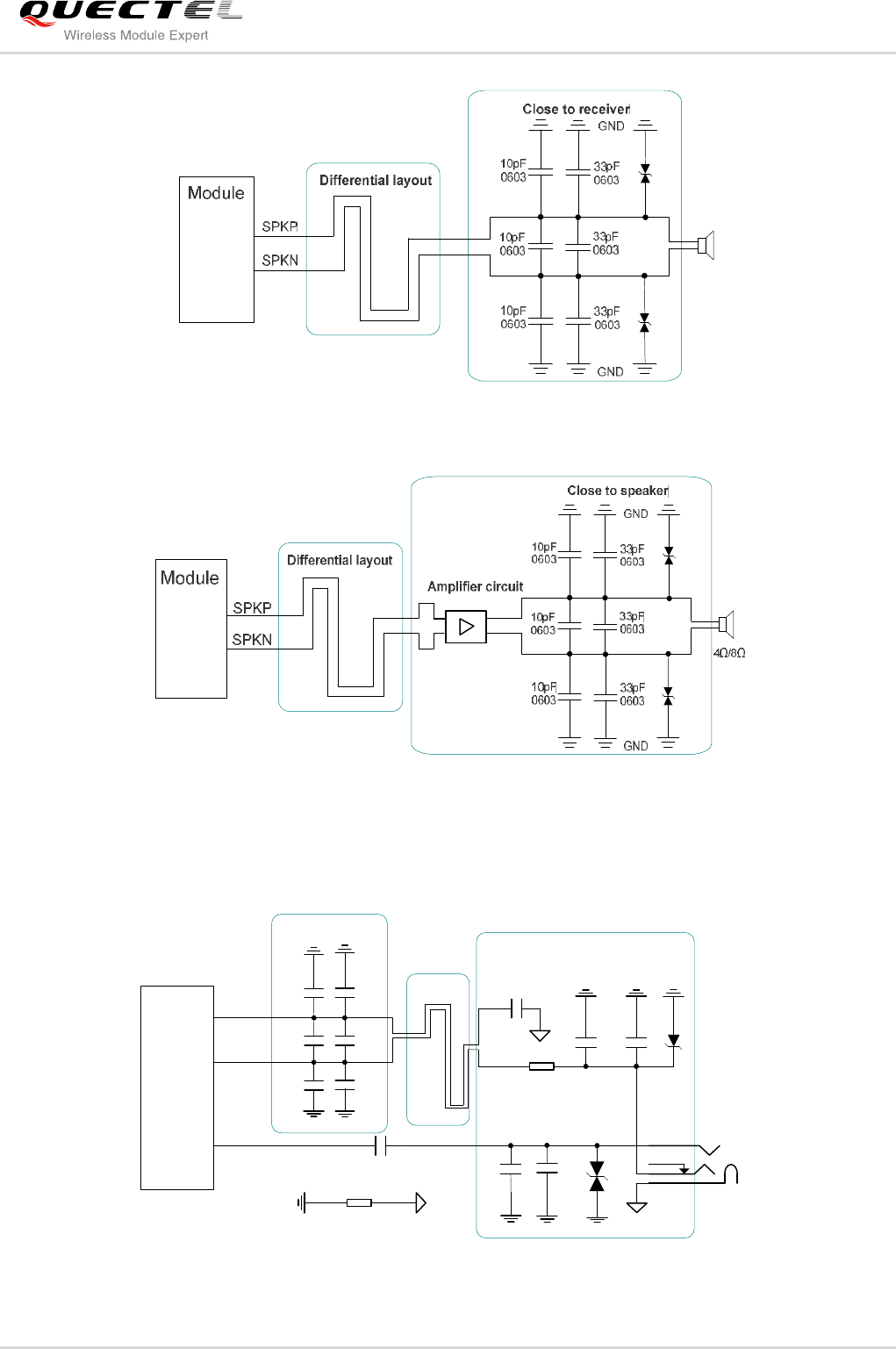
Figure 13: Reference Design of Receiver
Figure 14: Reference Design with an Amplifier for Speaker
Texas Instruments TPA6205A1 is recommended for a suitable differential audio amplifier.
1
2
4
3
MICP
22uF
68R
33pF
GND
AGND
Close to connector
33pF
10pF
GND
Module 4.7uF
SPKP
Close to module
GND
33pF
33pF
Differential
layout
33pF
MICN 0603
0603
0603 0603
06030603
0603
10pF
GND
10pF
0603
0603
0603
10pF
10pF
0R
GND AGND
Earphone
Interface
Figure 15: Reference Design of Earphone

UMTS/HSDPA Module Series
UC15 Mini PCIe Hardware Design
UC15_Mini_PCIe_Hardware_Design Confidential / Released 29 / 40
You can use AT+QMIC to adjust the input gain level of microphone, use AT+CLVL to adjust the output
gain level of receiver and speaker. AT+QSIDET is to set the side-tone gain level. For more details, please
refer to document [2].
The 33pF capacitors and 10pF capacitors are applied for filtering out 850/900/1800/1900MHz RF
interference. However, the self-resonant frequency point of capacitor largely depends on the material and
production technique. Therefore, you should depend on the capacitor vendor to choose the most suitable
capacitor for filtering out GSM850, EGSM900, DCS1800 and PCS1900 separately.
In order to decrease radio or other signal interference, RF antenna should be kept away from audio
interface and audio alignment. Power alignment and audio alignment should not be parallel, and power
alignment should be far away from audio alignment. The differential audio traces should be placed
according to the differential signal layout rules.
3.8. Control Signals
The following table shows the pin definition of control signals.
Table 14: Description of Control Signal Pins
3.8.1. W_DISABLE# Signal
UC15 Mini PCIe provides W_DISABLE# signal to disable wireless communications through hardware
operation. The following table shows the radio operational states of module. Please refer to document [2]
for related AT commands.
Table 15: Radio Operational States
Pin No.
Pin Name I/O
Power Domain
Description
20 W_DISABLE#
DI
3.3V Disable wireless communications. Active
low.
22 PERST#
DI
3.3V Functional reset to the card. Active low
pulse.
42 LED_WWAN#
OC
— Active-low LED signal for indicating the
state of the card.
W_DISABLE# AT Commands Radio Operation
High Level AT+CFUN=1 Enabled
UMTS/HSDPA Module Series
UC15 Mini PCIe Hardware Design
UC15_Mini_PCIe_Hardware_Design Confidential / Released 30 / 40
3.8.2. PERST# Signal
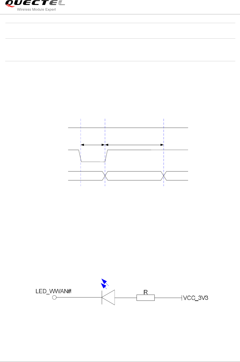
The PERST# signal can be used to force a hardware reset on the card. You can reset the module by
driving the PERST# to a low level voltage for 0.05~0.2s and then release it. The reset scenario is
illustrated in the following figure.
VIL ≤ 0.35V
VIH ≥ 2.3V
VCC_3V3
0.05~0.2s
RESETTING
Module
Status RUNNING
PERST#
RUNNING
≥ 5s
Figure 16: Timing of Resetting Module
3.8.3. LED_WWAN# Signal
The LED_WWAN# signal of UC15 Mini PCIe is used to indicate the network status of the module, which
can absorb the current up to 40mA. According to the following circuit, in order to reduce the current of the
LED, a resistor must be placed in series with the LED. The LED is emitting light when the LED_WWAN#
output signal is active low.
Figure 17: Reference Circuit of LED_WWAN#
The following table shows the indications of network status of the LED_WWAN# signal.
High Level AT+CFUN=0
AT+CFUN=4 Disabled
Low Level
AT+CFUN=0
AT+CFUN=1
AT+CFUN=4
Disabled
UMTS/HSDPA Module Series
UC15 Mini PCIe Hardware Design
UC15_Mini_PCIe_Hardware_Design Confidential / Released 31 / 40
Table 16: Indication of Network Status
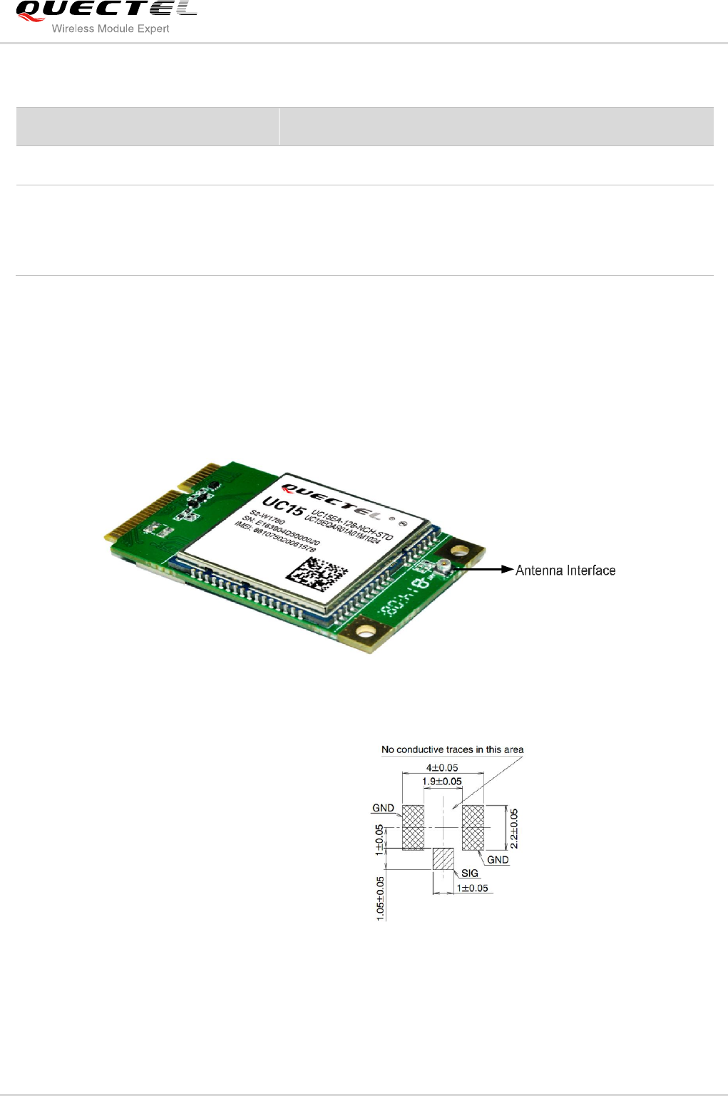
3.9. Antenna Interface
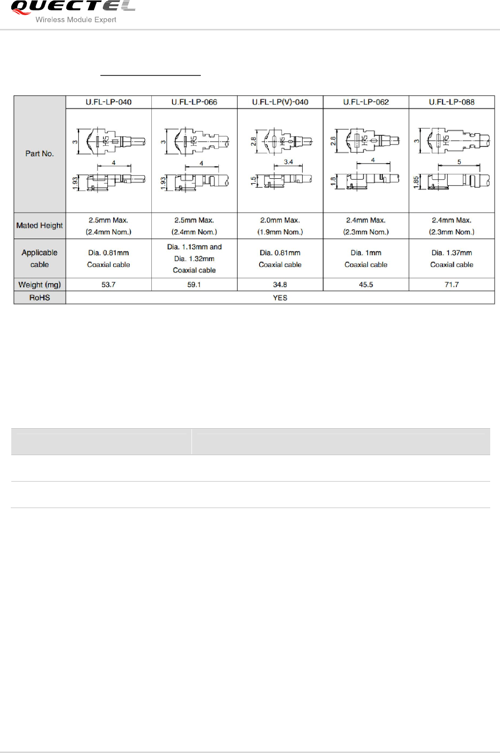
The following figures show the location of antenna interface and describe the overall size of RF
connector.
Figure 18: UC15 Mini PCIe Antenna Interface
Figure 19: Dimensions of the RF Connector (Unit: mm)
LED_WWAN# Description
Low Level (Light on) Registered network.
High-impedance (Light off)
No network coverage or not registered.
W_DISABLE# signal is in low level.
AT+CFUN=0 or AT+CFUN=4.
Module gets into sleep mode.
UMTS/HSDPA Module Series
UC15 Mini PCIe Hardware Design
UC15_Mini_PCIe_Hardware_Design Confidential / Released 32 / 40
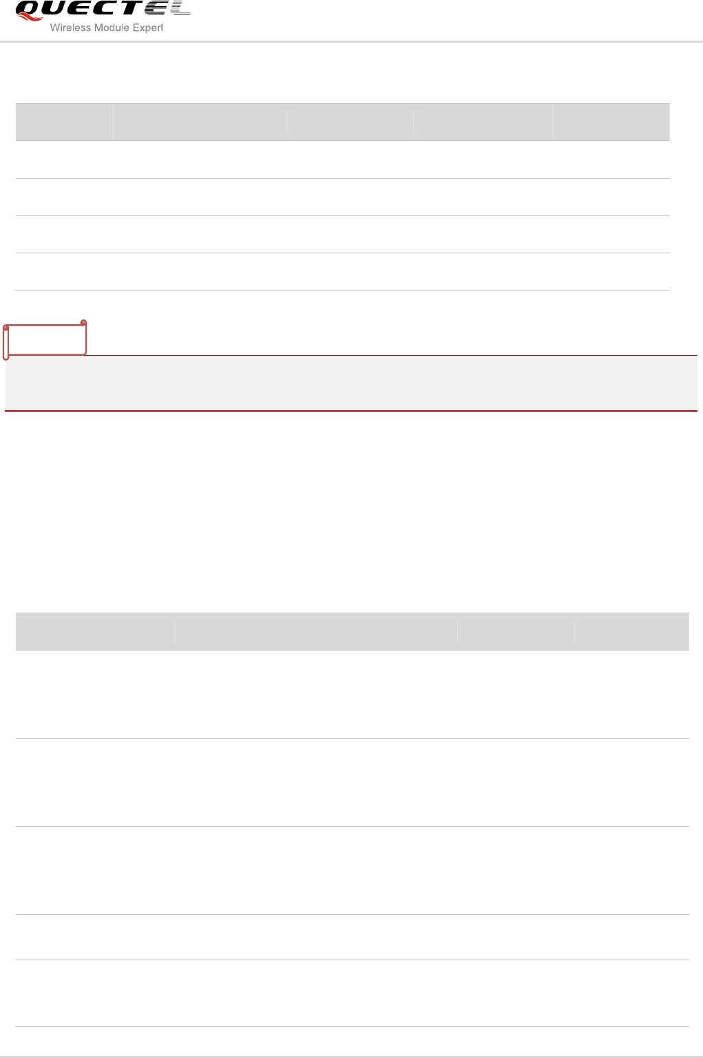
You can use U.FL-LP serial connector listed in the following figure to match the ECT818000117. For more
details, please visit http://www.hirose.com.
Figure 20: Mechanicals of UF.L-LP Connectors
The following table shows the requirements on GSM/UMTS antenna.
Table 17: Antenna Requirements
Type Requirements
GSM850/EGSM900/UMTS850 Cable insertion loss < 0.5dB.
DCS1800/PCS1900//UMTS1900 Cable insertion loss < 0.9dB.

UMTS/HSDPA Module Series
UC15 Mini PCIe Hardware Design
UC15_Mini_PCIe_Hardware_Design Confidential / Released 33 / 40
4 Electrical and Radio Characteristics
4.1. General Description
This chapter mainly describes the following electrical and radio characteristics of UC15 Mini PCIe:
Power supply requirements
IO requirements
Current consumption
RF characteristics
ESD characteristics
4.2. Power Supply Requirements
The input voltage of UC15 Mini PCIe is 3.3V±9%, as specified by PCI Express Mini CEM Specifications
1.2. The following table shows the power supply requirements of UC15 Mini PCIe.
Table 18: Power Supply Requirements
4.3. IO Requirements
The following table shows the IO requirements of UC15 Mini PCIe.
Parameter Description Min. Typ. Max. Unit
VCC_3V3 Power supply 3.0 3.3 3.6 V
UMTS/HSDPA Module Series
UC15 Mini PCIe Hardware Design
UC15_Mini_PCIe_Hardware_Design Confidential / Released 34 / 40
Table 19: IO Requirements
1. VDDIO=2.6V for PCM interface, and 3.3V for other digital interfaces.
2. The maximum value of VIL for PERST# signal is 0.35V.
4.4. Current Consumption
The current consumptions of UC15 Mini PCIe in different scenarios are respectively shown below.
Table 20: Current Consumption
Parameter Description Min. Max. Unit
VIH Input high voltage 0.7*VDDIO VDDIO+0.3 V
VIL Input low voltage -0.3 0.2*VDDIO V
VOH Output high voltage VDDIO-0.5 VDDIO V
VOL Output low voltage 0 0.4 V
Description Conditions Typ. Unit
Sleep
GSM (USB disconnected) @DRX=2
GSM (USB disconnected) @DRX=9
UMTS (USB disconnected) @DRX=6
UMTS (USB disconnected) @DRX=9
5.5
3.5
5.8
3.3
mA
Idle
GSM(USB connected) @DRX=2
GSM(USB disconnected) @DRX=2
UMTS(USB connected) @DRX=6
UMTS(USB disconnected) @DRX=6
80
50
80
45
mA
GSM
Voice Call
GSM850 @PCL5
EGSM900 @PCL5
DCS1800 @PCL0
PCS1900 @PCL0
340
320
262
260
mA
UMTS
Voice Call
UMTS850 @max power
UMTS1900 @max power
570
650 mA
GPRS Data Transfer
GSM850 (1UL/1DL) @PCL5
GSM850 (2UL/3DL) @PCL5
EGSM900 (1UL/1DL) @PCL5
300
410
290
mA
NOTES
UMTS/HSDPA Module Series
UC15 Mini PCIe Hardware Design
UC15_Mini_PCIe_Hardware_Design Confidential / Released 35 / 40
4.5. RF Characteristics
The following tables show output power and receiving sensitivity of conducted RF of UC15 Mini PCIe
module.
Table 21: Output Power of Conducted RF
Table 22: Receiving Sensitivity of Conducted RF
EGSM900 (2UL/3DL) @PCL5
DCS1800 (1UL/1DL) @PCL0
DCS1800 (2UL/3DL) @PCL0
PCS1900 (1UL/1DL) @PCL0
PCS1900 (2UL/3DL) @PCL0
401
241
333
235
320
UMTS Data Transfer UMTS850 (HSDPA) @max power
UMTS1900 (HSDPA) @max power
500
570 mA
Frequency Max. Min.
GSM850 33dBm±2dB 5dBm±5dB
EGSM900 33dBm±2dB 5dBm±5dB
DCS1800 30dBm±2dB 0dBm±5dB
PCS1900 30dBm±2dB 0dBm±5dB
GSM850 (8-PSK) 27dBm±3dB 5dBm±5dB
EGSM900 (8-PSK) 27dBm±3dB 5dBm±5dB
DCS1800 (8-PSK) 26dBm+3/-4dB 0dBm±5dB
PCS1900 (8-PSK) 26dBm+3/-4dB 0dBm±5dB
UMTS850 24dBm+1/-3dB -56dBm±5dB
UMTS1900 24dBm+1/-3dB -56dBm±5dB
Frequency Receive Sensitivity (Typ.)
GSM850 -108.5dBm
UMTS/HSDPA Module Series
UC15 Mini PCIe Hardware Design
UC15_Mini_PCIe_Hardware_Design Confidential / Released 36 / 40
4.6. ESD Characteristics
The following table shows characteristics of UC15 Mini PCIe ESD.
Table 23: ESD Characteristics
EGSM900 -108.5dBm
DCS1800 -108.5dBm
PCS1900 -108.5dBm
UMTS850 -110dBm
UMTS1900 -110dBm
Parameter Contact Discharge Air Discharge Unit
Power Supply and GND ±5 ±10 kV
Antenna Interface ±4 ±8 kV
USB Interface ±4 ±8 kV
USIM Interface ±4 ±8 kV
Others ±0.5 ±1 kV
UMTS/HSDPA Module Series
UC15 Mini PCIe Hardware Design
UC15_Mini_PCIe_Hardware_Design Confidential / Released 37 / 40
5 Mechanical Dimensions
5.1. General Description
This chapter mainly describes the following dimensions of UC15 Mini PCIe:
Mechanical Dimensions of UC15 Mini PCIe
Standard Dimensions of Mini PCI Express
Packaging
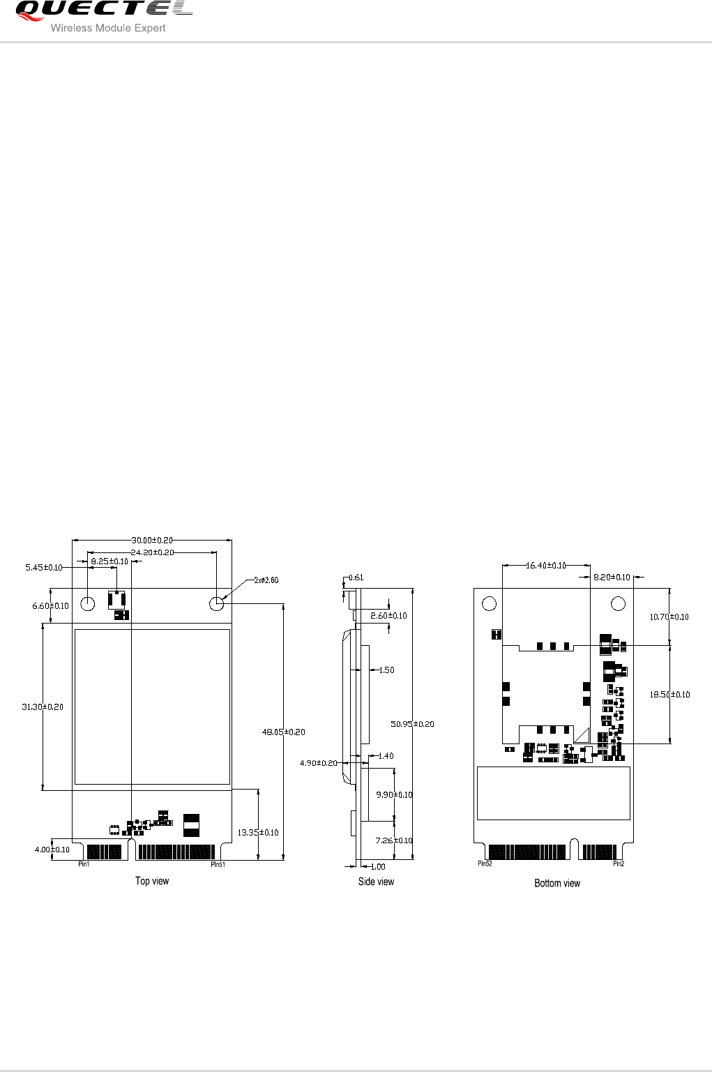
5.2. Mechanical Dimensions of UC15 Mini PCIe
Figure 21: Mechanical Dimensions of UC15 Mini PCIe (Unit: mm)
UMTS/HSDPA Module Series
UC15 Mini PCIe Hardware Design
UC15_Mini_PCIe_Hardware_Design Confidential / Released 38 / 40
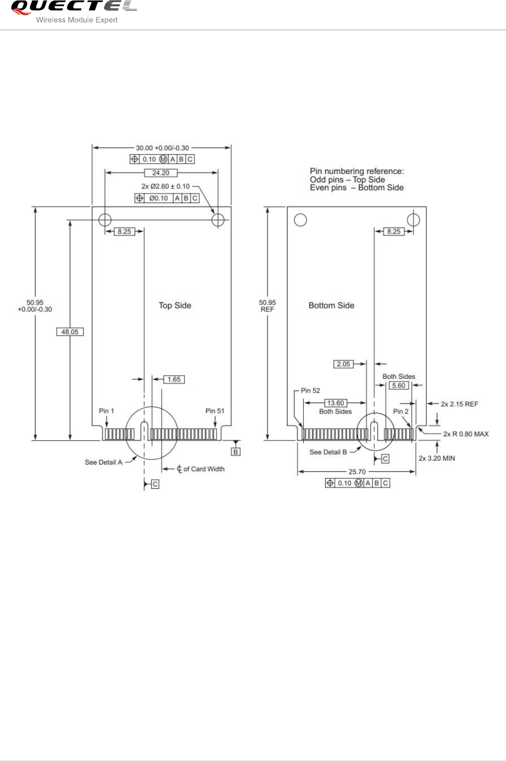
5.3. Standard Dimensions of Mini PCI Express
The following figure shows the standard Dimensions of Mini PCI Express. Please refer to document [1]
for detail A and detail B.
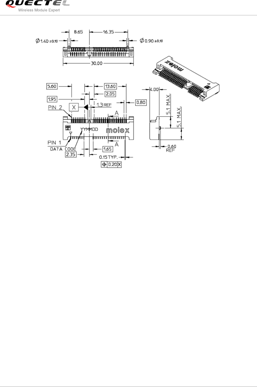
Figure 22: Standard Dimensions of Mini PCI Express (Unit: mm)
UC15 Mini PCIe adopts a standard Mini PCI Express connector which compiles with the standards listed
in the document [1]. The following figure takes the Molex 679100002 as an example.
UMTS/HSDPA Module Series
UC15 Mini PCIe Hardware Design
UC15_Mini_PCIe_Hardware_Design Confidential / Released 39 / 40
Figure 23: Dimensions of the Mini PCI Express Connector (Unit: mm)
5.4. Packaging
The UC15 Mini PCIe is packaged in tray. Each tray contains 10pcs of modules. The smallest package of
UC15 Mini PCIe contains 100pcs.
UMTS/HSPA Module
UC15 Mini PCIe Hardware Design
UC15_Mini_PCIe_Hardware_Design Confidential / Released 40 / 40
6 Appendix Reference
Table 24: Related Documents
Table 25: Terms and Abbreviations
SN Document Name Remark
[1] PCI Express Mini Card Electromechanical
Specification Revision 1.2 Mini PCI Express Specification.
[2] Quectel_UC15_AT_Commands_Manual UC15 AT Commands Manual.
Abbreviation Description
bps Bits Per Second
CS Coding Scheme
CSD Circuit Switched Data
CTS Clear to Send
DCE Data Communications Equipment (typically module)
DL Down Link
DTE Data Terminal Equipment (typically computer, external controller)
DTR Data Terminal Ready
EMC Electromagnetic Compatibility
ESD Electrostatic Discharge
GMSK Gaussian Minimum Shift Keying
GSM Global System for Mobile Communications
HSDPA High Speed Downlink Packet Access

UMTS/HSPA Module
UC15 Mini PCIe Hardware Design
UC15_Mini_PCIe_Hardware_Design Confidential / Released 41 / 40
I/O Input/Output
kbps Kilo Bits Per Second
LED Light Emitting Diode
Mbps Million Bits Per Second
MMS Multimedia Messaging Service
MO Mobile Originated
MT Mobile Terminated
PAP Password Authentication Protocol
PCM Pulse Code Modulation
PDU Protocol Data Unit
PPP Point-to-Point Protocol
RF Radio Frequency
RX Receive Direction
SIM Subscriber Identification Module
SMS Short Message Service
TDMA Time Division Multiple Access
TE Terminal Equipment
TX Transmitting Direction
UART Universal Asynchronous Receiver & Transmitter
UL Up Link
UMTS Universal Mobile Telecommunications System
URC Unsolicited Result Code
USSD Unstructured Supplementary Service Data
WCDMA Wideband Code Division Multiple Access