Quectel Wireless Solutions 201408UG95 UMTS/HSPA Module User Manual
Quectel Wireless Solutions Company Limited UMTS/HSPA Module
UserManual.wiki
>
Quectel Wireless Solutions
>
201408UG95 User Manual
User manual
Navigation menu
Upload a User Manual
Namespaces
Wiki Guide
HTML
PDF
Info
Views
User Manual
Discussion / Help
Navigation
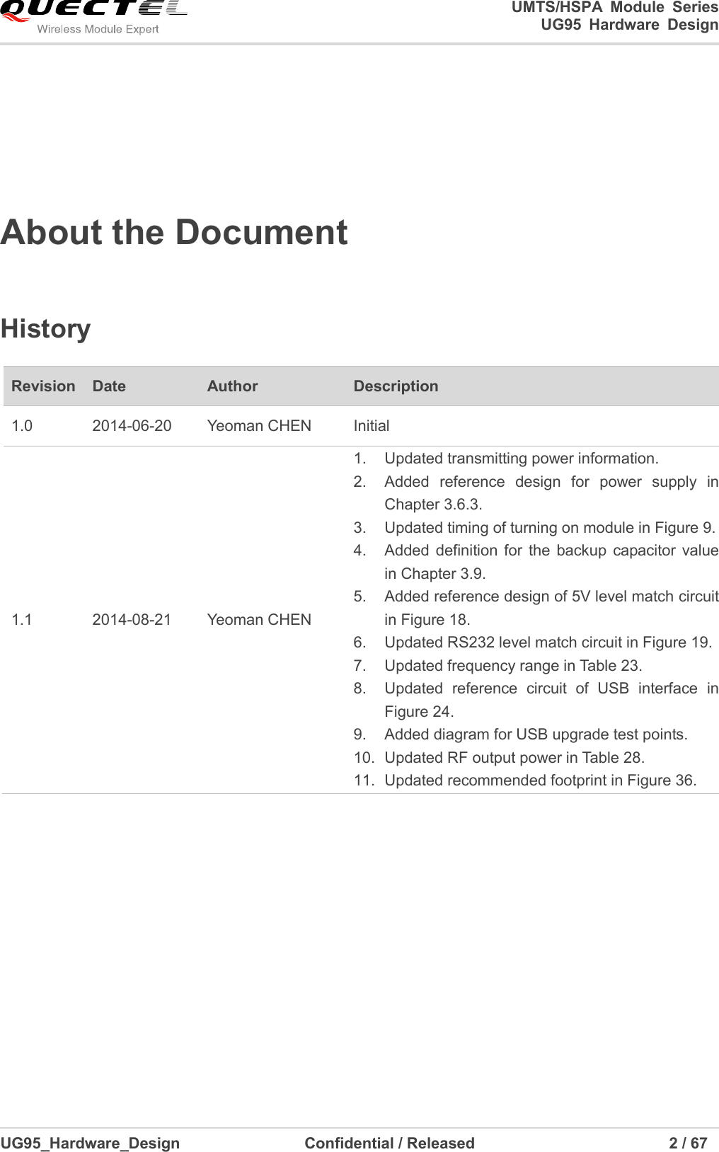
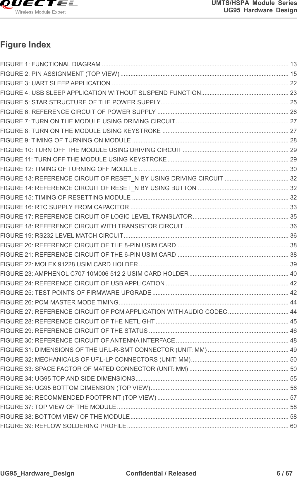
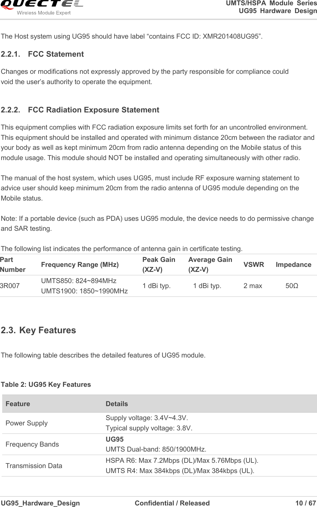
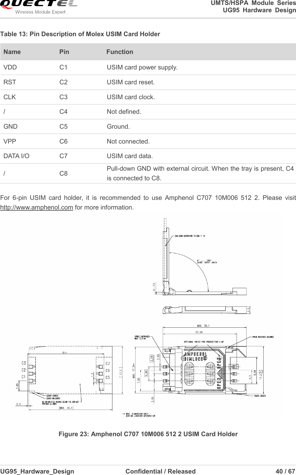
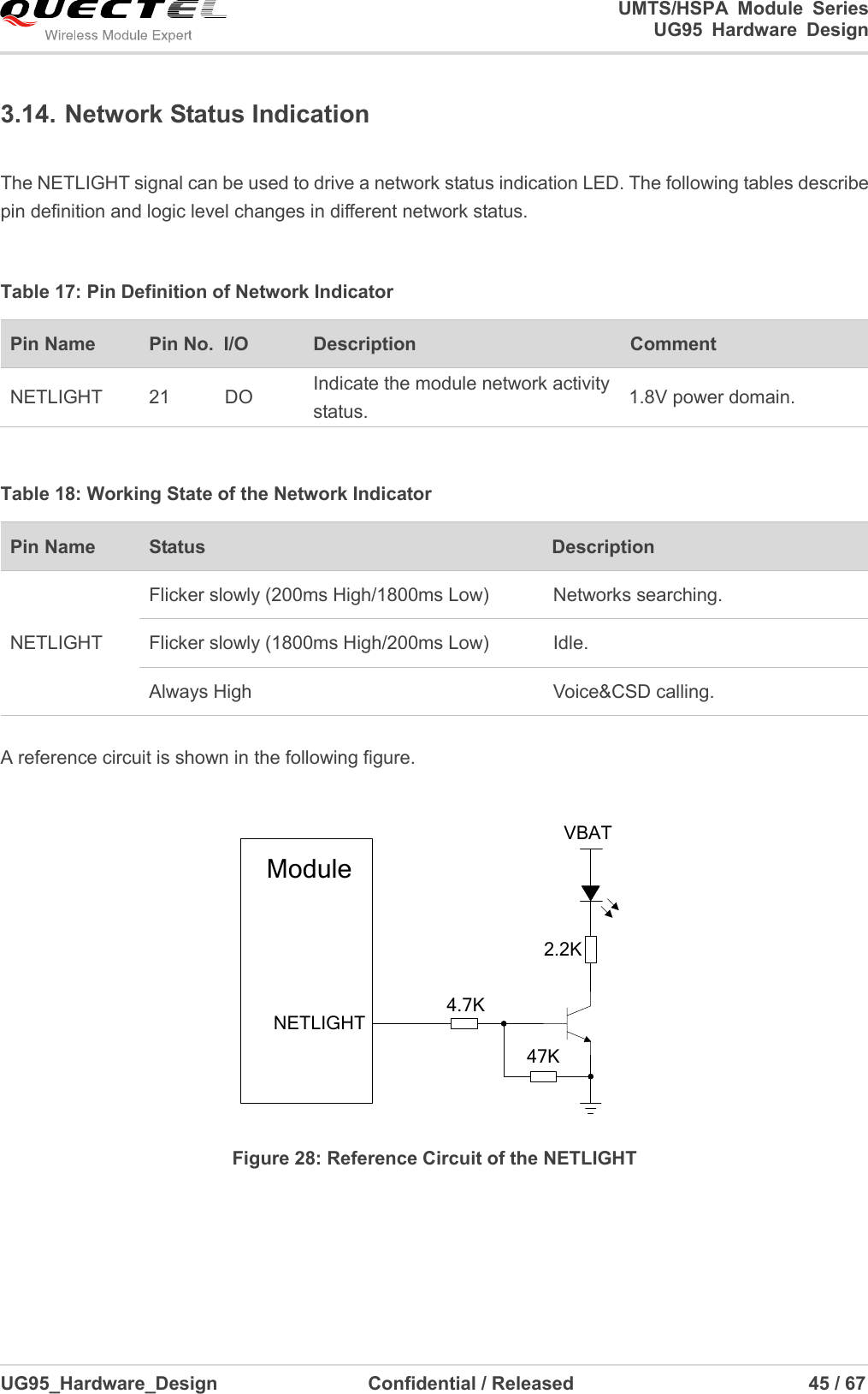
![UMTS/HSPA Module Series UG95 Hardware Design UG95_Hardware_Design Confidential / Released 13 / 67 Figure 1: Functional Diagram 2.5. Evaluation Board In order to help you to develop applications with UG95, Quectel supplies an evaluation board (UC20-EVB), RS-232 to USB cable, USB data cable, power adapter, earphone, antenna and other peripherals to control or test the module. For details, please refer to document [2].](https://usermanual.wiki/Quectel-Wireless-Solutions/201408UG95/User-Guide-2390890-Page-14.png)
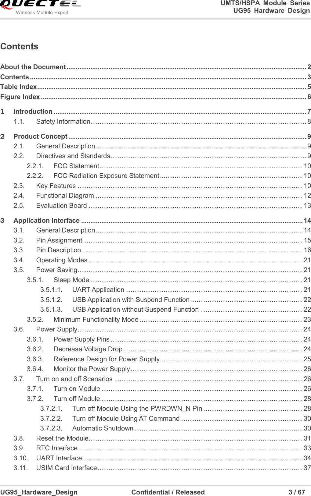
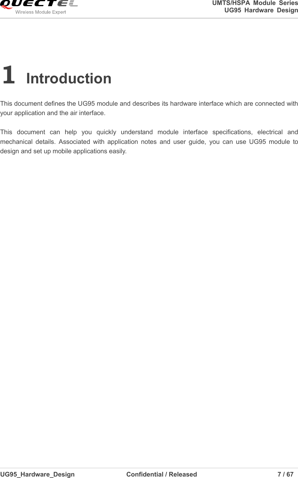
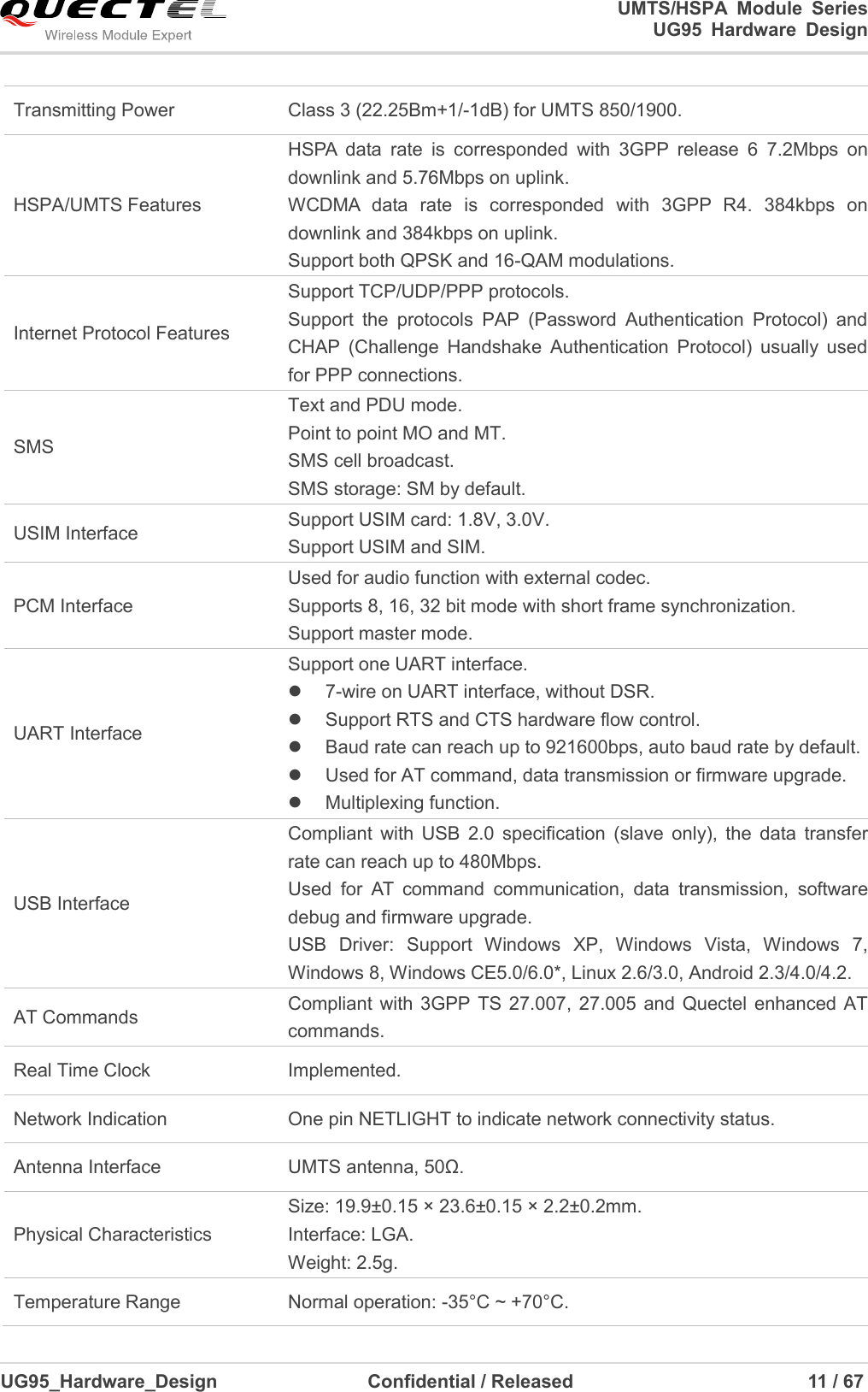
![UMTS/HSPA Module Series UG95 Hardware Design UG95_Hardware_Design Confidential / Released 23 / 67 Supply power to USB_VBUS will wake up the module. The following figure shows the connection between the module and application processor. USB_VBUSUSB_DPUSB_DMAP_READYVDDUSB_DPUSB_DMGPIOModule ProcessorRI EINTPower SwitchGPIOGND GND Figure 4: USB Sleep Application without Suspend Function In sleep mode, the module can still receive paging message, SMS, voice call and TCP/UDP data from the network normally. AP_READY is under development. 3.5.2. Minimum Functionality Mode Minimum functionality mode reduces the functionality of the module to minimum level, thus minimizes the current consumption at the same time. This mode can be set as below: Command AT+CFUN provides the choice of the functionality levels: <fun>=0, 1, 4. AT+CFUN=0: Minimum functionality, RF part and USIM card will be closed. AT+CFUN=1: Full functionality (by default). AT+CFUN=4: Disable RF function (airplane mode). All AT commands related to RF function are not accessible. For detailed information about command AT+CFUN, please refer to document [1]. NOTE](https://usermanual.wiki/Quectel-Wireless-Solutions/201408UG95/User-Guide-2390890-Page-24.png)
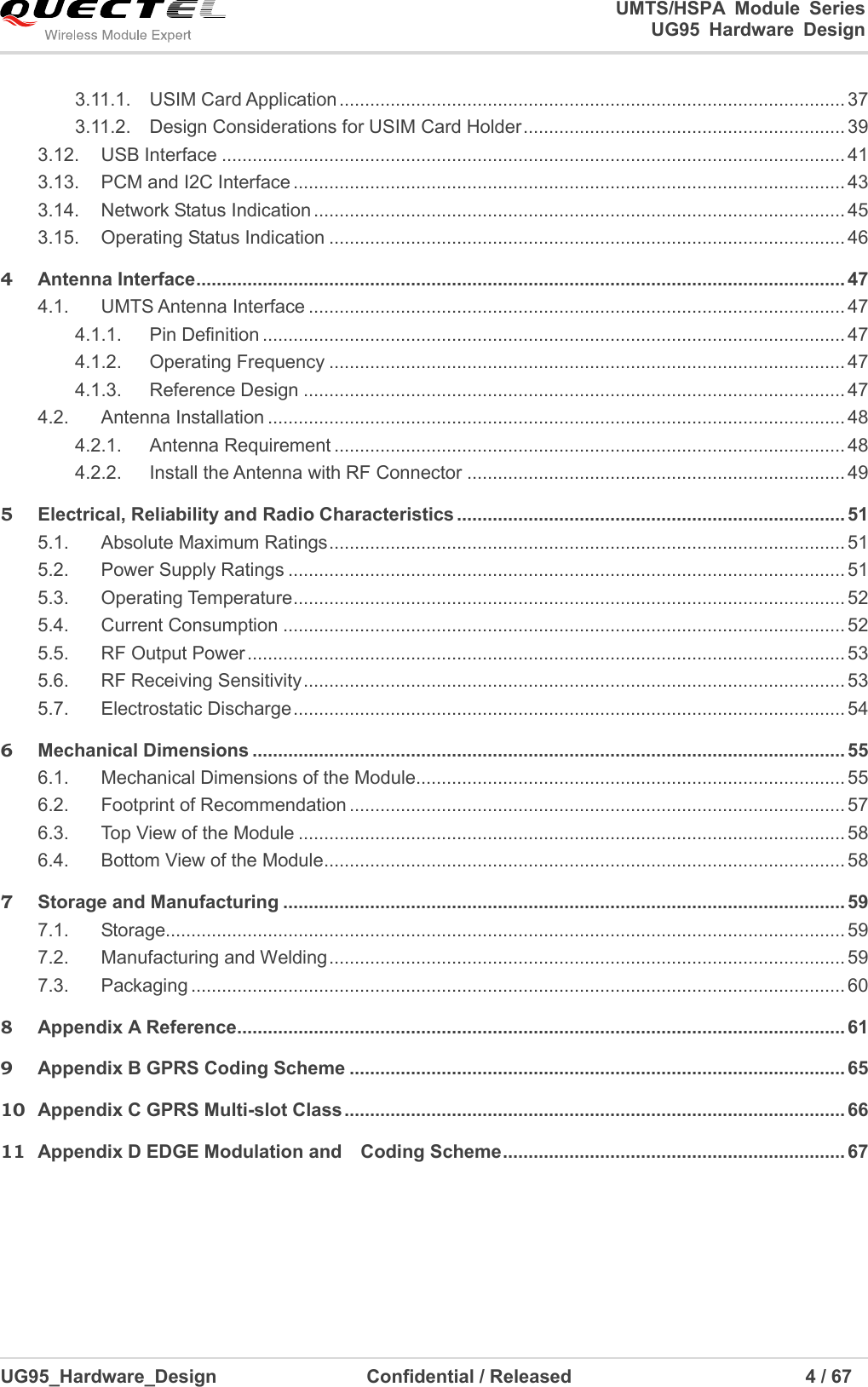
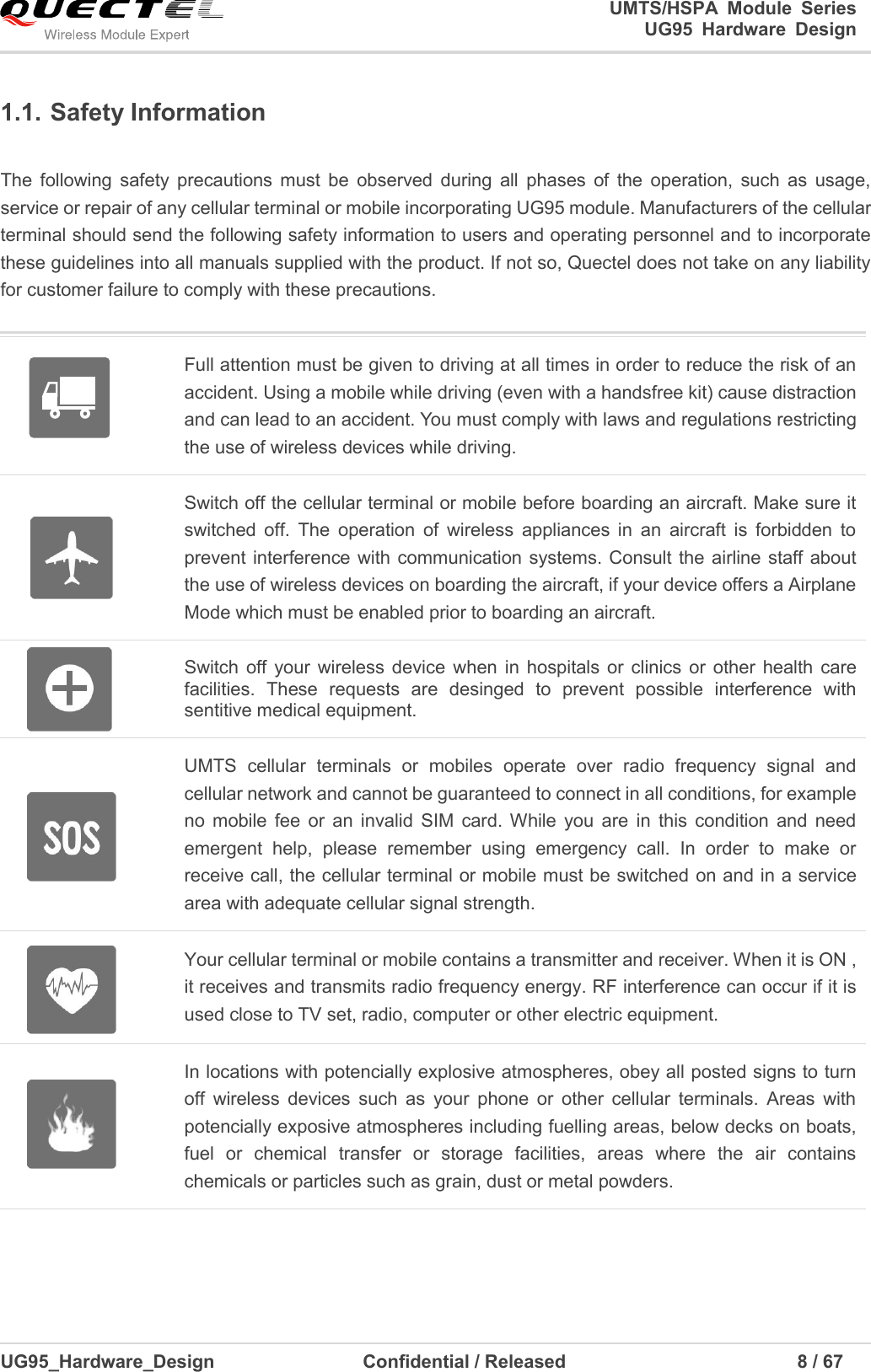
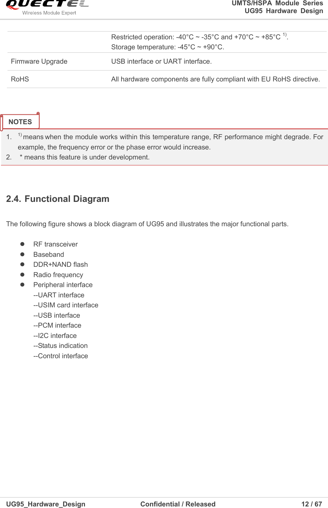
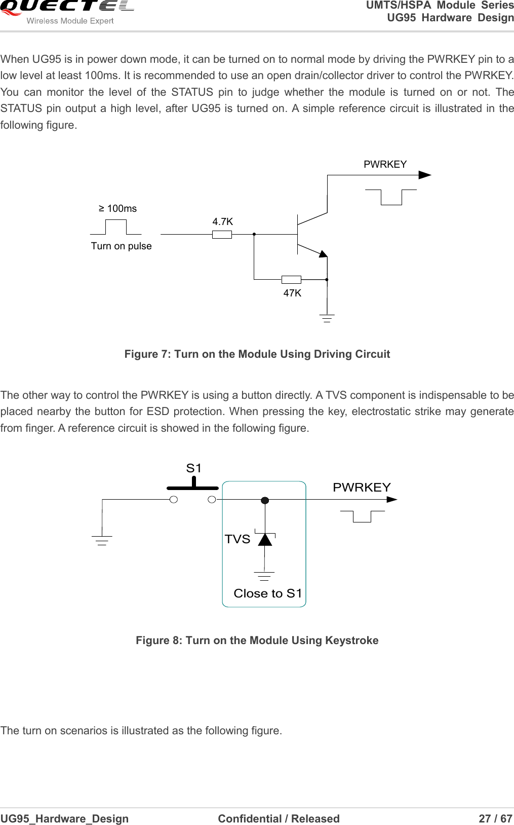
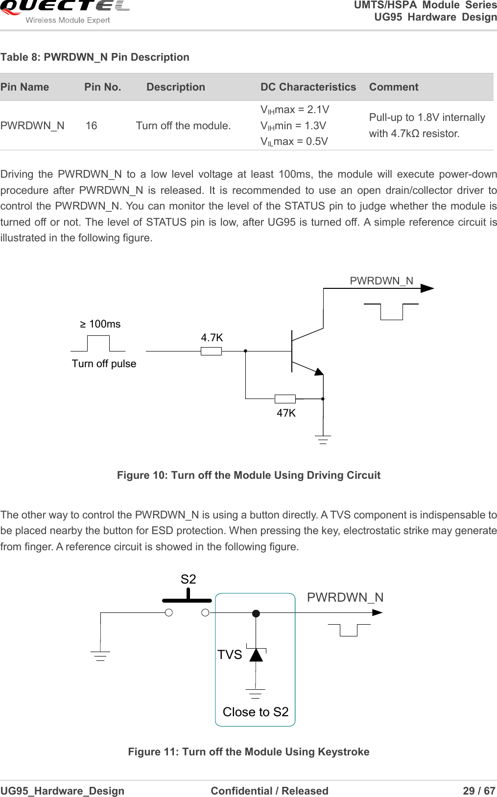
![UMTS/HSPA Module Series UG95 Hardware Design UG95_Hardware_Design Confidential / Released 26 / 67 DC_INC1 C2MIC29302WU U1IN OUTENGNDADJ2 4135VBAT 100nF C3470uFC4100nFR2100K47KR3470uF470R51K R4R11%1%MCU_POWER_ON/OFF 47K4.7KR5R6 Figure 6: Reference Circuit of Power Supply It is suggested to disconnect power supply to turn off the module when the module is in abnormal state. 3.6.4. Monitor the Power Supply You can use the AT+CBC command to monitor the VBAT_BB voltage value. For more details, please refer to document [1]. 3.7. Turn on and off Scenarios 3.7.1. Turn on Module Turn on the module using the PWRKEY. The following table shows the pin definition of PWRKEY. Table 7: PWRKEY Pin Description Pin Name Pin No. Description DC Characteristics Comment PWRKEY 15 Turn on the module. VIHmax = 2.1V VIHmin = 1.3V VILmax = 0.5V Pull-up to 1.8V internally with 200kΩ resistor. NOTE](https://usermanual.wiki/Quectel-Wireless-Solutions/201408UG95/User-Guide-2390890-Page-27.png)
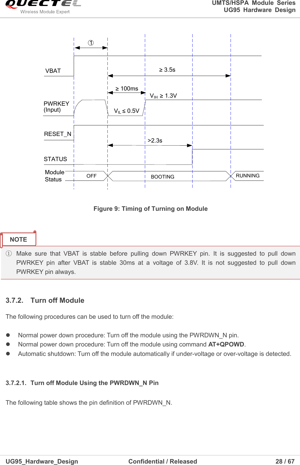
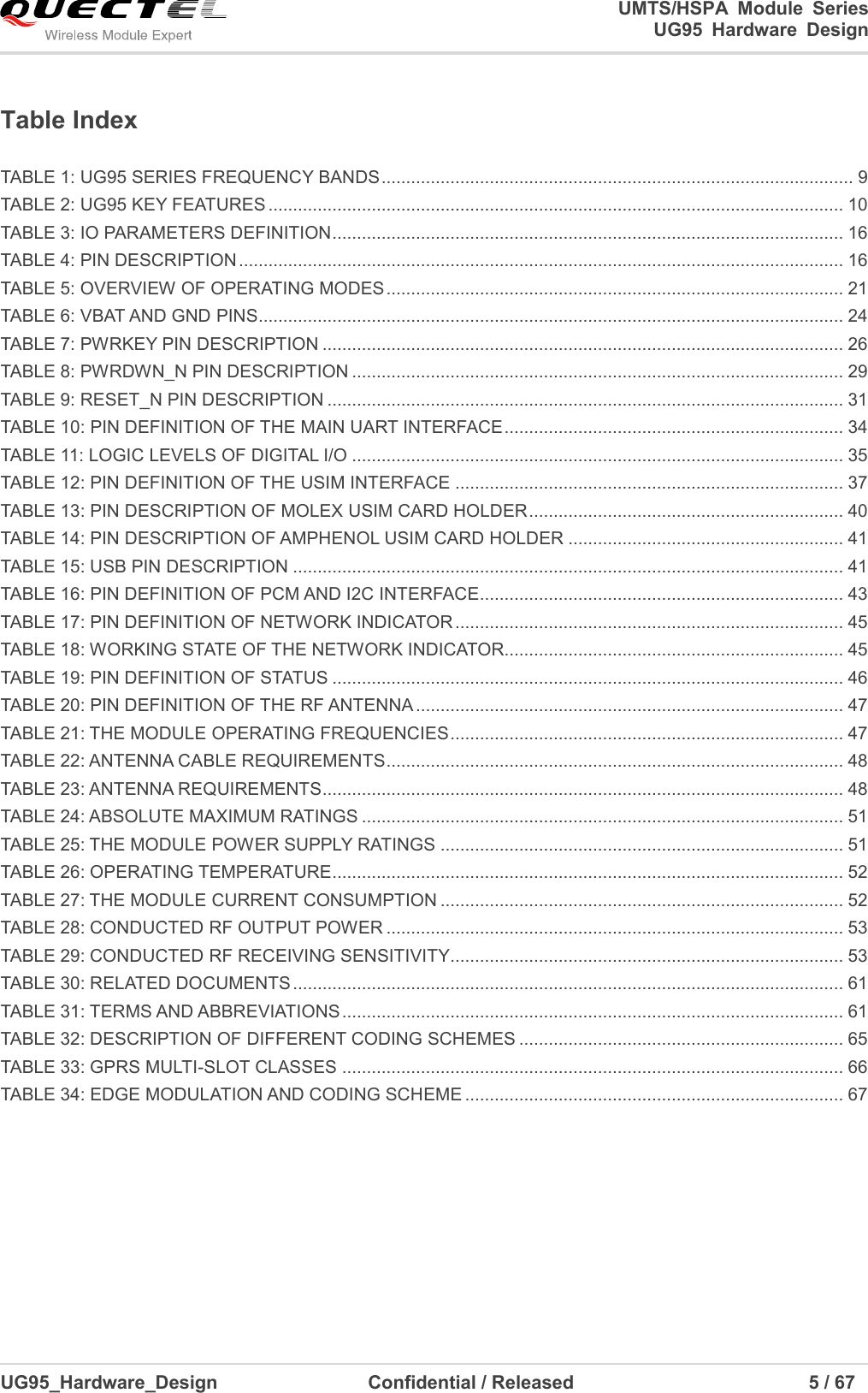
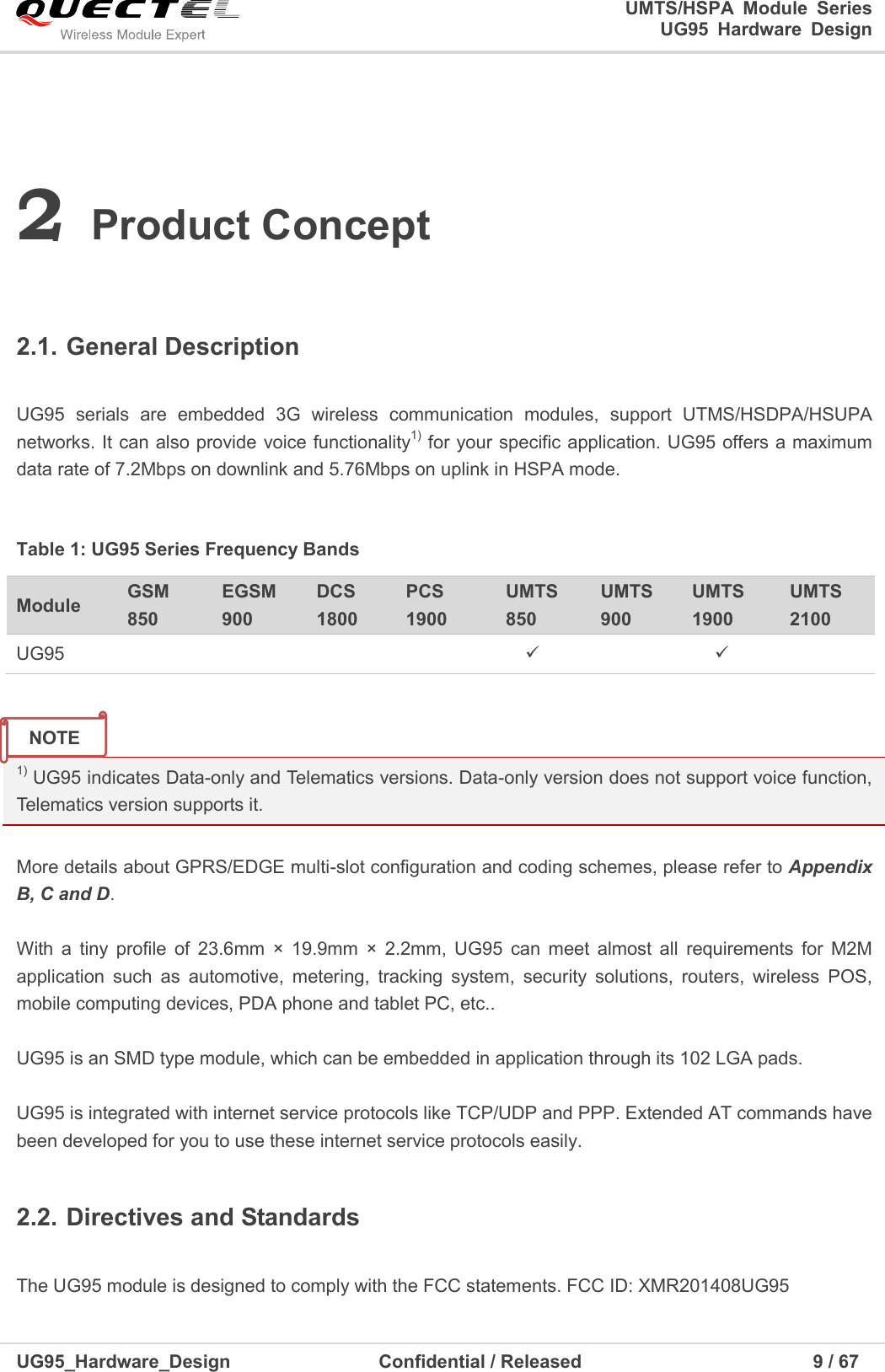
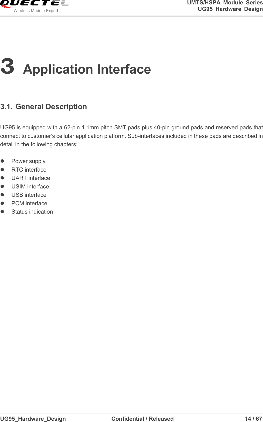
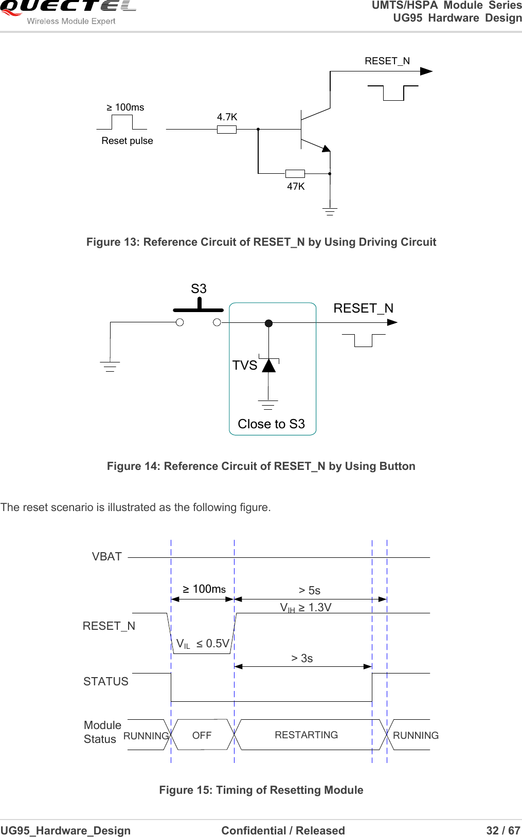
![UMTS/HSPA Module Series UG95 Hardware Design UG95_Hardware_Design Confidential / Released 30 / 67 The power-down scenario is illustrated as the following figure. VBATPWRDWN_N(Input)Log off network about 1s to 60s≥ 100msRUNNING Power-down procedure OFFModuleStatusSTATUS Figure 12: Timing of Turning off Module During power-down procedure, module will log off network and save important data. After logging off, module sends out “OK”, and then sends out “POWERED DOWN” and shut down the internal power supply. The power on VBAT pins is not allowed to turn off before the URC “POWERED DOWN” is output to avoid data loss. If logging off is not done within 60s, module will shut down internal power supply forcibly. After that moment, the module enters the power down mode, no other AT commands can be executed and only the RTC is still active. The power down mode can also be indicated by the STATUS pin. 3.7.2.2. Turn off Module Using AT Command It is also a safe way to use AT command AT+QPOWD to turn off the module, which is similar to turning off the module via PWRDWN_N Pin. Please refer to document [1] for details about the AT command of AT+QPOWD. 3.7.2.3. Automatic Shutdown The module will constantly monitor the voltage applied on the VBAT, if the voltage ≤ 3.5V, the following URC will be presented: +QIND: “vbatt”,-1](https://usermanual.wiki/Quectel-Wireless-Solutions/201408UG95/User-Guide-2390890-Page-31.png)
![UMTS/HSPA Module Series UG95 Hardware Design UG95_Hardware_Design Confidential / Released 31 / 67 If the voltage ≥ 4.21V, the following URC will be presented: +QIND: “vbatt”,1 The uncritical voltage is 3.4V to 4.3V, If the voltage > 4.3V or < 3.4V the module would automatically shut down itself. If the voltage < 3.4V, the following URC will be presented: +QIND: “vbatt”,-2 If the voltage > 4.3V, the following URC will be presented: +QIND: “vbatt”,2 1. The value of voltage threshold can be revised by AT command, refer to document [1] for details. 2. Automatic shutdown is under development. 3.8. Reset the Module The RESET_N can be used to reset the module. Table 9: RESET_N Pin Description Pin Name Pin No. Description DC Characteristics Comment RESET_N 17 Reset the module. VIHmax = 2.1V VIHmin = 1.3V VILmax = 0.5V Pull-up to 1.8V internally with 200kΩ resistor. Active low. You can reset the module by driving the RESET_N to a low level voltage for more than 100ms and then releasing. The recommended circuit is similar to the PWRKEY control circuit. You can use open drain/collector driver or button to control the RESET_N. NOTES](https://usermanual.wiki/Quectel-Wireless-Solutions/201408UG95/User-Guide-2390890-Page-32.png)
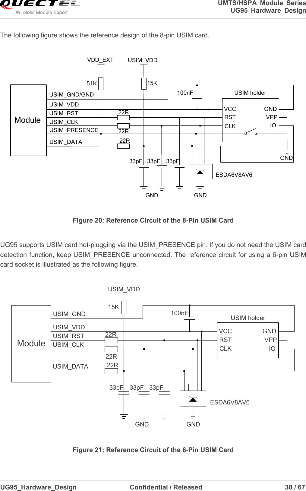
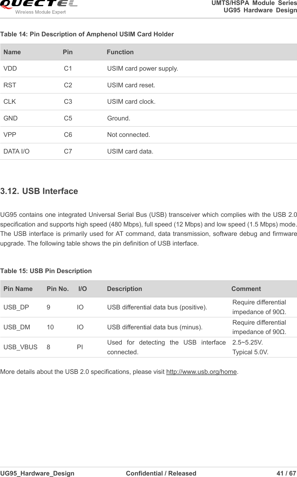
![UMTS/HSPA Module Series UG95 Hardware Design UG95_Hardware_Design Confidential / Released 37 / 67 1. The module disables the hardware flow control by default. When hardware flow control is required, RTS and CTS should be connected to the host. AT command AT+IFC=2,2 is used to enable hardware flow control. AT command AT+IFC=0,0 is used to disable the hardware flow control. For more details, please refer to document [1]. 2. Rising edge on DTR will let the module exit from the data mode by default. It can be disabled by AT commands. Refer to document [1] for details. 3. DCD is used as data mode indication. Refer to document [1] for details. 4. It is suggested to set USB_DP, USB_DM and USB_VBUS pins as test points and then place these test points on the DTE for debug. 3.11. USIM Card Interface 3.11.1. USIM Card Application The USIM card interface circuitry meets ETSI and IMT-2000 SIM interface requirements. Both 1.8V and 3.0V USIM cards are supported. Table 12: Pin Definition of the USIM Interface Pin Name Pin No. I/O Description Comment USIM_PRESENCE 42 DI USIM card detection input. 1.8V power domain. USIM_VDD 43 PO Power supply for USIM card. Either 1.8V or 3.0V is supported by the module automatically. USIM_RST 44 DO Reset signal of USIM card. USIM_DATA 45 IO Data signal of USIM card. Pull-up to USIM_VDD with 4.7k resistor internally. USIM_CLK 46 DO Clock signal of USIM card. USIM_GND 47 Specified ground for USIM card. NOTES](https://usermanual.wiki/Quectel-Wireless-Solutions/201408UG95/User-Guide-2390890-Page-38.png)
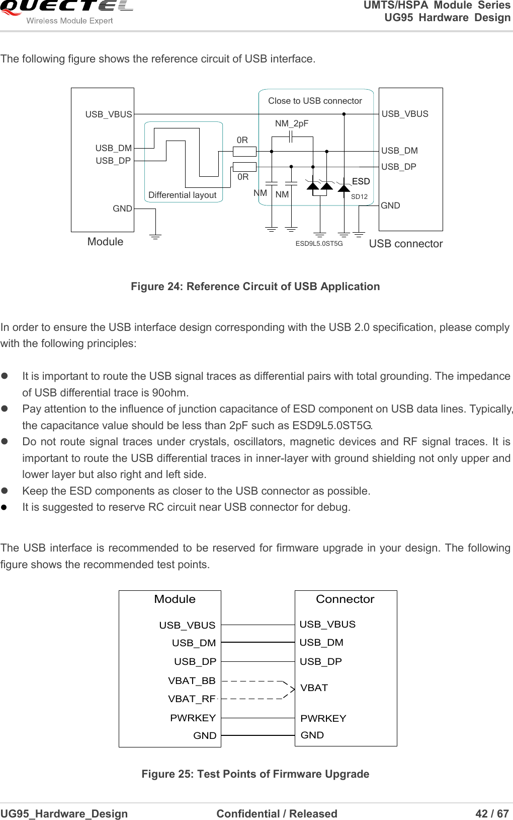
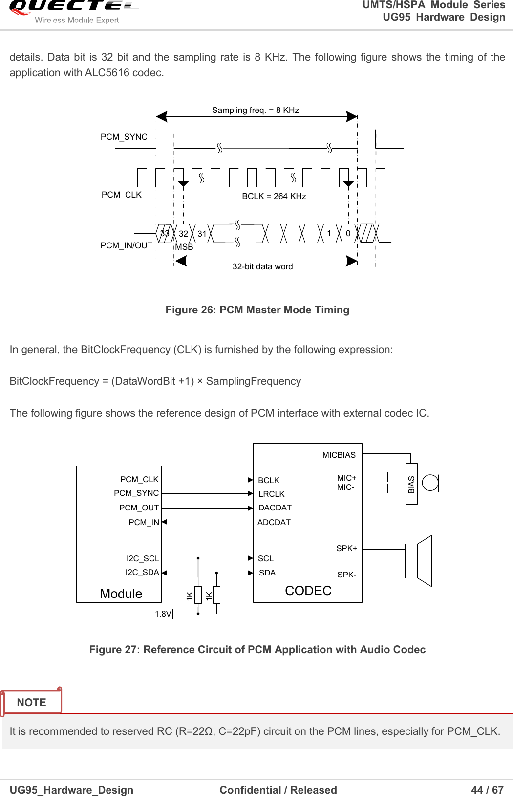
![UMTS/HSPA Module Series UG95 Hardware Design UG95_Hardware_Design Confidential / Released 43 / 67 1. UG95 module can only be used as a slave device. 2. It is suggested to set USB_DP, USB_DM and USB_VBUS pins as test points and then place these test points on the DTE for debug. 3. USB interface supports software debug and firmware upgrade by default. 3.13. PCM and I2C Interface UG95 provides one Pulse Code Modulation (PCM) digital interface for audio design, which supports the following features: Supports 8, 16, 32 bit mode with short frame synchronization, the PCM support 8 bit mode by default since the PCM codec default configuration is AT+QDAI=1. Refer to document [1] for more details. Supports master mode. Supports audio sample rate 8 kHz. The following table shows the pin definition of PCM and I2C interface which can be applied on audio codec design. Table 16: Pin Definition of PCM and I2C Interface Pin Name Pin No. I/O Description Comment PCM_CLK 4 IO PCM data bit clock. 1.8V power domain. PCM_SYNC 5 IO PCM data frame sync signal. 1.8V power domain. PCM_IN 6 DI PCM data input. 1.8V power domain. PCM_OUT 7 DO PCM data output. 1.8V power domain. I2C_SCL 40 DO I2C serial clock. Require external pull-up resistor. I2C_SDA 41 IO I2C serial data. Require external pull-up resistor. In PCM audio format the MSB of the channel included in the frame (PCM_SYNC) is clocked on the second CLK falling edge after the PCM_SYNC pulse rising edge. The period of the PCM_SYNC signal (frame) lasts for Data word bit +1 clock pulses. UG95’s firmware has integrated the configuration on ALC5616 application with I2C interface. You can execute command AT+QDAI=3 to configure the ALC5616 codec, and refer to document [1] for more NOTE](https://usermanual.wiki/Quectel-Wireless-Solutions/201408UG95/User-Guide-2390890-Page-44.png)
![UMTS/HSPA Module Series UG95 Hardware Design UG95_Hardware_Design Confidential / Released 59 / 67 7 Storage and Manufacturing 7.1. Storage UG95 is stored in the vacuum-sealed bag. The restriction of storage condition is shown as below. Shelf life in sealed bag is 12 months at < 40ºC/90%RH. After this bag is opened, devices that will be subjected to reflow solder or other high temperature process must be: Mounted within 72 hours at factory conditions of ≤ 30ºC/60%RH. Stored at <10% RH. Devices require bake, before mounting, if: Humidity indicator card is >10% when read 23ºC±5ºC. Mounted for more than 72 hours at factory conditions of ≤ 30ºC/60% RH. If baking is required, devices may be baked for 48 hours at 125ºC±5ºC. As plastic container cannot be subjected to high temperature, module needs to be taken out from container to high temperature (125ºC) bake. If shorter bake times are desired, please refer to IPC/JEDECJ-STD-033 for bake procedure. 7.2. Manufacturing and Welding The squeegee should push the paste on the surface of the stencil that makes the paste fill the stencil openings and penetrate to the PCB. The force on the squeegee should be adjusted so as to produce a clean stencil surface on a single pass. To ensure the module soldering quality, the thickness of stencil at the hole of the module pads should be 0.13mm. For details, please refer to document [6]. NOTE](https://usermanual.wiki/Quectel-Wireless-Solutions/201408UG95/User-Guide-2390890-Page-60.png)
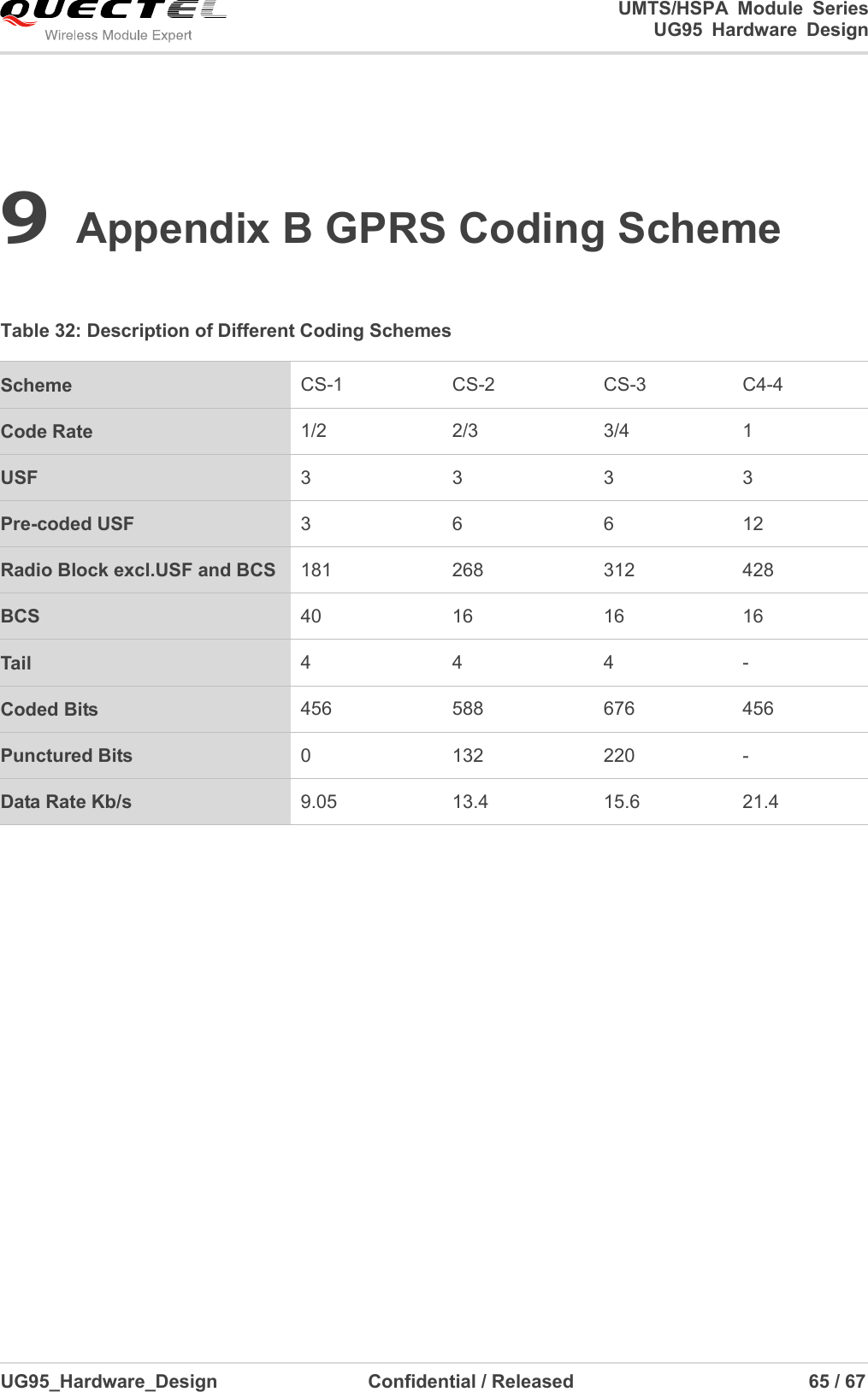
![UMTS/HSPA Module Series UG95 Hardware Design UG95_Hardware_Design Confidential / Released 61 / 67 8 Appendix A Reference Table 30: Related Documents SN Document Name Remark [1] Quectel_UG95_AT_Commands_Manual UG95 AT Commands Manual [2] Quectel_UC20_EVB_User_Guide UC20 EVB User Guide [3] Quectel_UG95_Reference_Design UG95 Reference Design [4] Quectel_UG95&M95_Reference_Design UG95 and M95 Compatible Reference Design [5] Quectel_UG95&M95_Compatible_Design UG95 and M95 Compatibility Design Specification [6] Quectel_Module_Secondary_SMT_User_Guide Module Secondary SMT User Guide Table 31: Terms and Abbreviations Abbreviation Description AMR Adaptive Multi-rate ARP Antenna Reference Point bps Bits Per Second CHAP Challenge Handshake Authentication Protocol CS Coding Scheme CSD Circuit Switched Data CTS Clear To Send DRX Discontinuous Reception DCE Data Communications Equipment (typically module) DTE Data Terminal Equipment (typically computer, external controller)](https://usermanual.wiki/Quectel-Wireless-Solutions/201408UG95/User-Guide-2390890-Page-62.png)