Quectel Wireless Solutions 201606EC21A LTE Module User Manual
Quectel Wireless Solutions Company Limited LTE Module Users Manual
UserManual.wiki
>
Quectel Wireless Solutions
>
201606EC21A User Manual
Users Manual
Navigation menu
Upload a User Manual
Namespaces
Wiki Guide
HTML
PDF
Info
Views
User Manual
Discussion / Help
Navigation


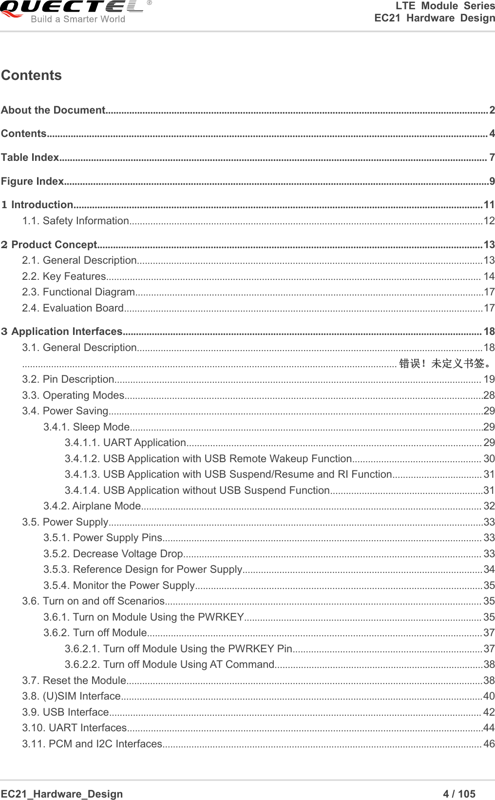

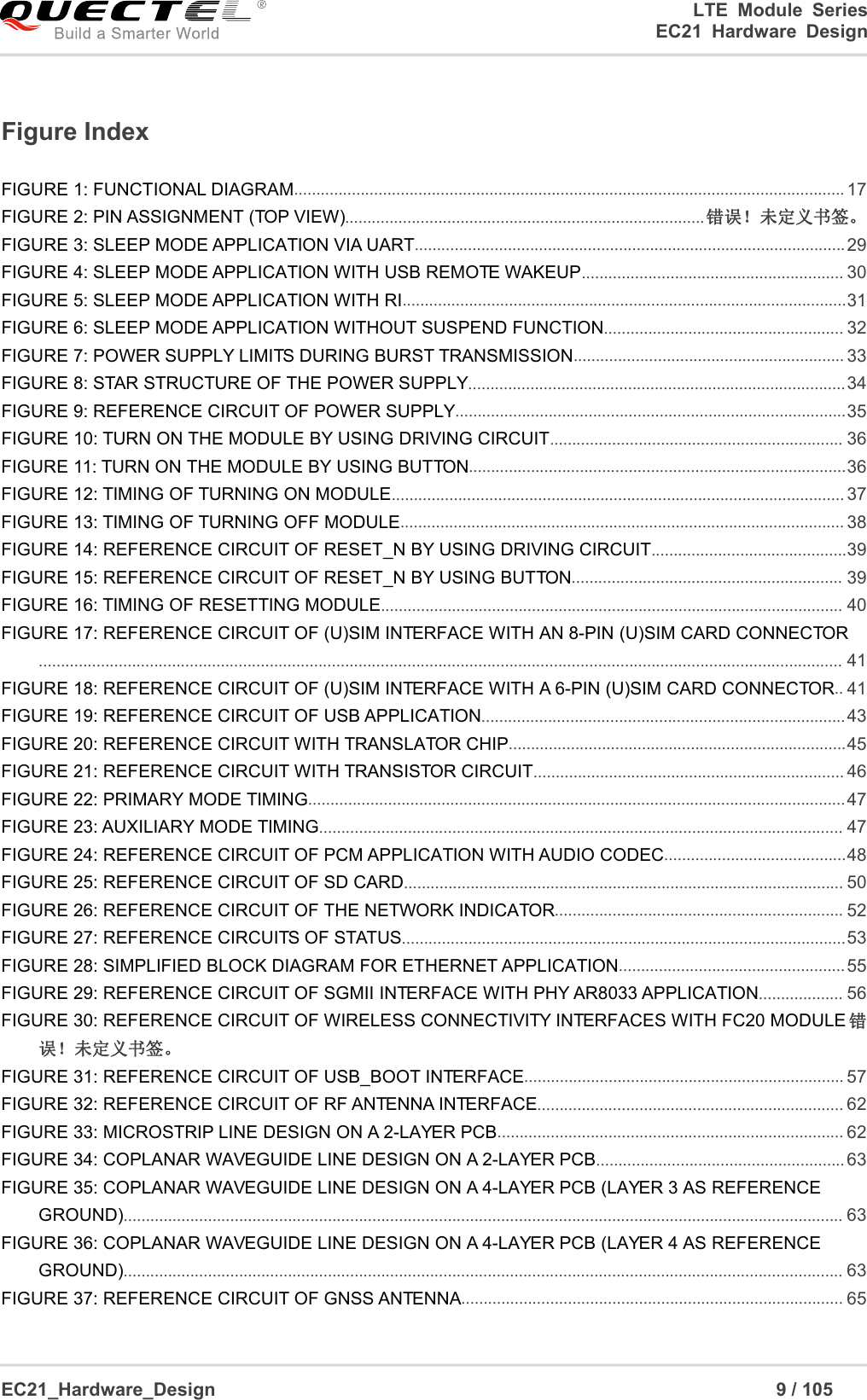


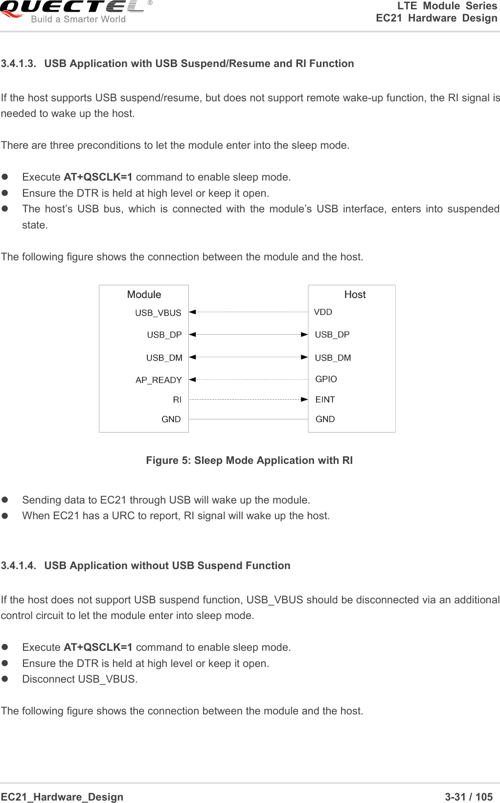
![LTE Module SeriesEC21 Hardware DesignEC21_Hardware_Design 3-32 / 105Figure 6: Sleep Mode Application without Suspend FunctionSwitching on the power switch to supply power to USB_VBUS will wake up the module.Please pay attention to the level match shown in dotted line between the module and the host. Refer todocument [1] for more details about EC21 power management application.3.4.2. Airplane ModeWhen the module enters into airplane mode, the RF function does not work, and all AT commandscorrelative with RF function will be inaccessible. This mode can be set via the following ways.Hardware:The W_DISABLE# pin is pulled up by default. Driving it to low level will let the module enter into airplanemode.Software:AT+CFUN command provides the choice of the functionality level through setting <fun> into 0, 1 or 4.AT+CFUN=0: Minimum functionality mode. Both (U)SIM and RF functions are disabled.AT+CFUN=1: Full functionality mode (by default).AT+CFUN=4: Airplane mode. RF function is disabled.1. W_DISABLE# control function is disabled in firmware by default. It can be enabled byAT+QCFG="airplanecontrol" command. This command is under development.2. The execution of AT+CFUN command will not affect GNSS function.NOTESNOTE](https://usermanual.wiki/Quectel-Wireless-Solutions/201606EC21A/User-Guide-3885852-Page-33.png)
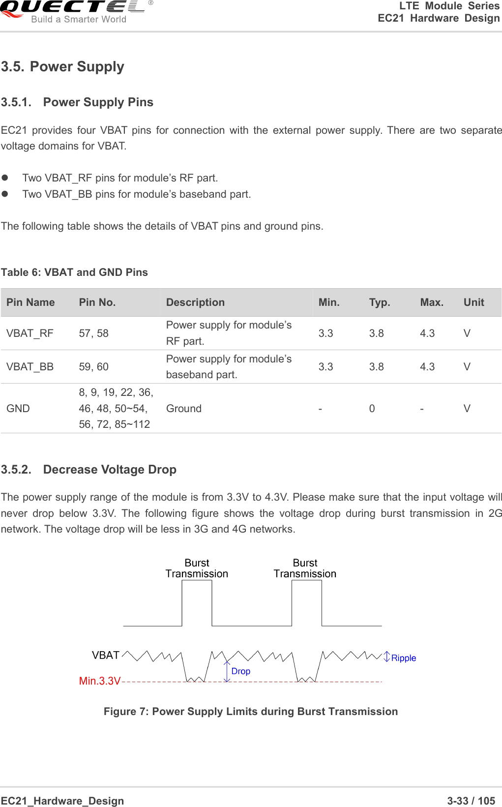
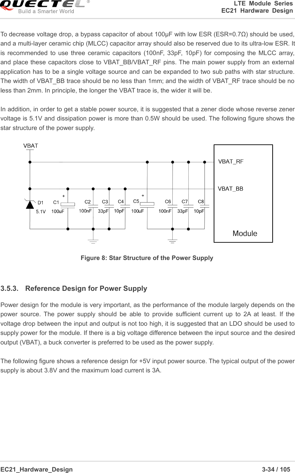
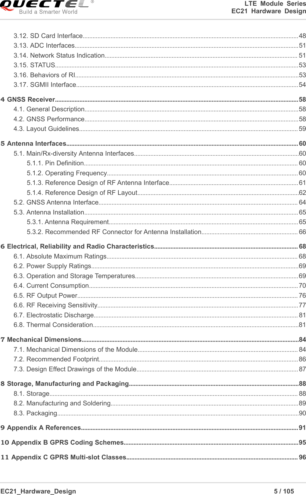
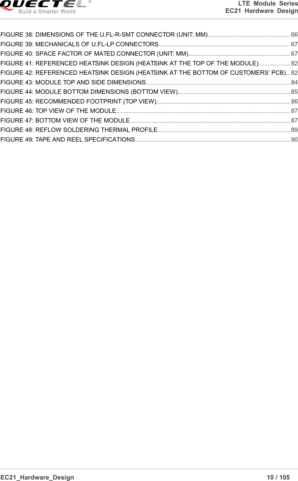
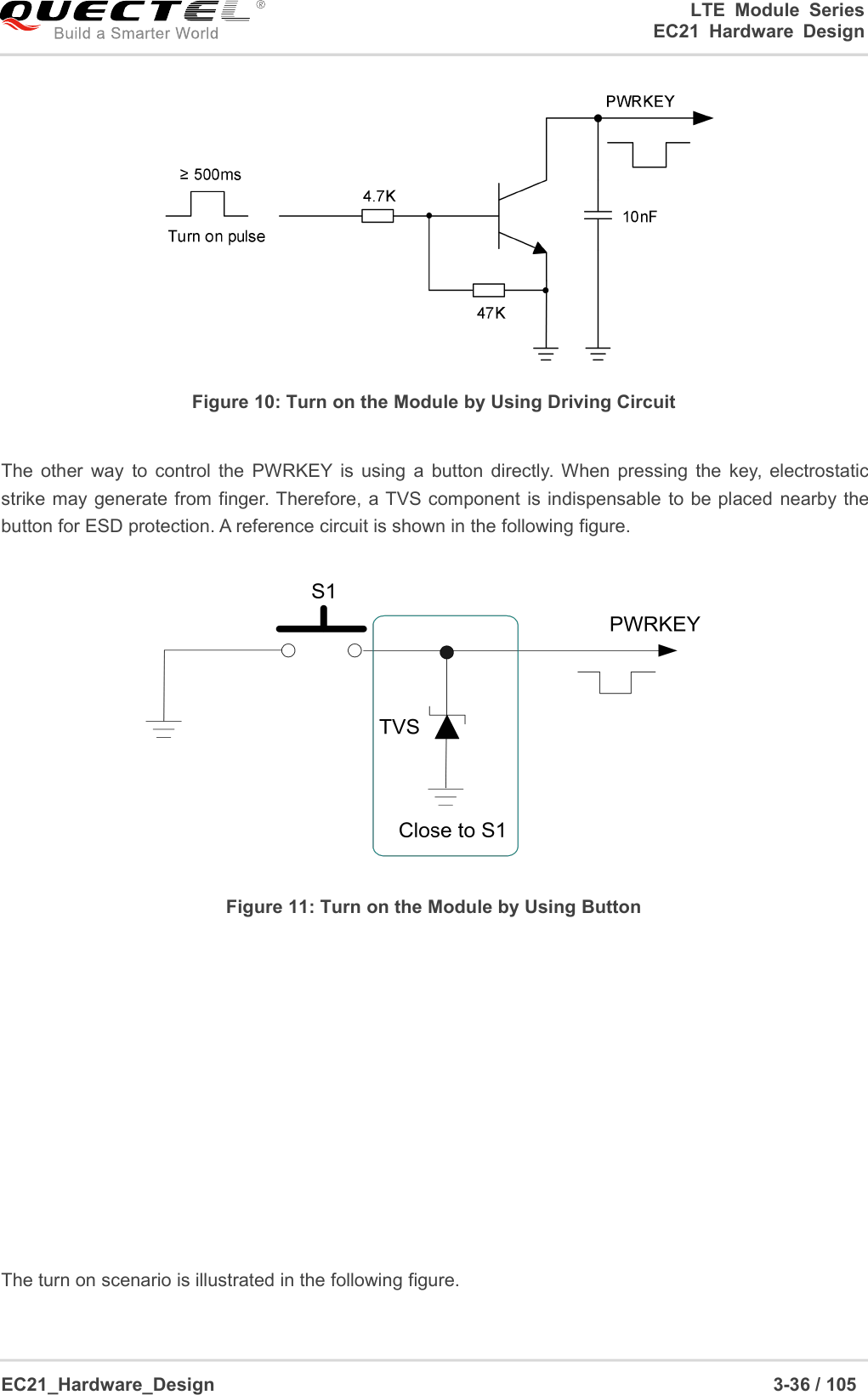
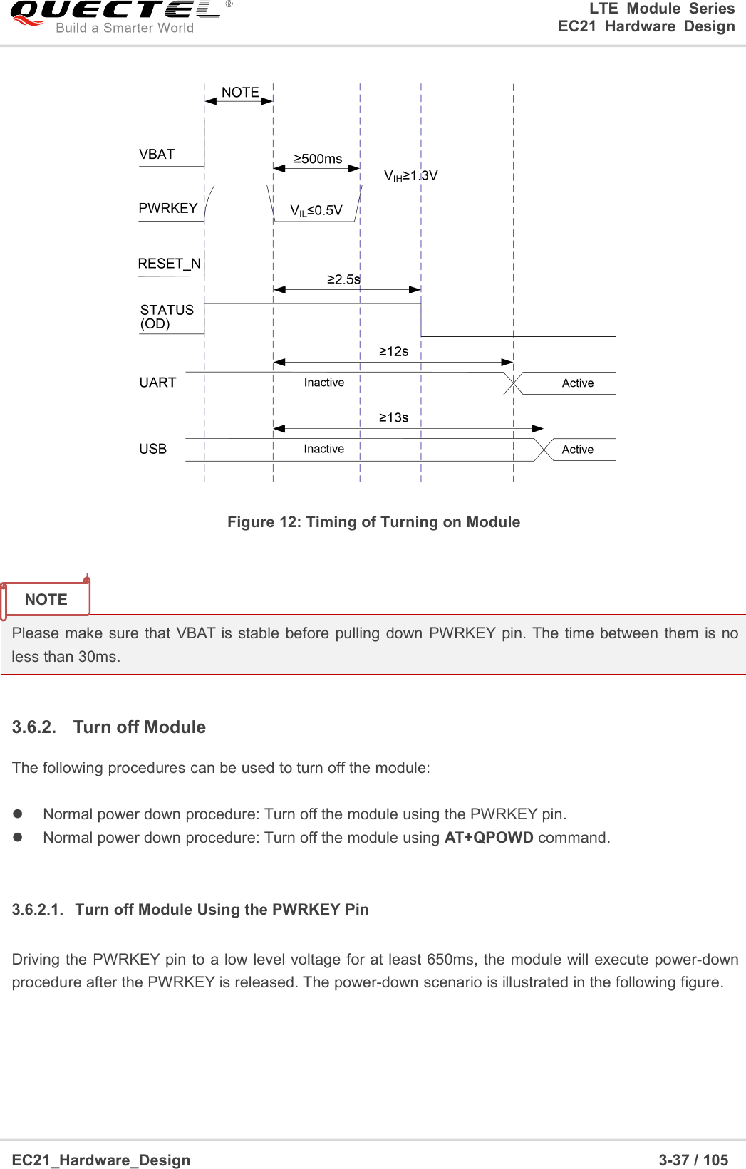
![LTE Module SeriesEC21 Hardware DesignEC21_Hardware_Design 3-35 / 105Figure 9: Reference Circuit of Power SupplyIn order to avoid damaging internal flash, please do not switch off the power supply when the moduleworks normally. Only after the module is shut down by PWRKEY or AT command, the power supply canbe cut off.3.5.4. Monitor the Power SupplyAT+CBC command can be used to monitor the VBAT_BB voltage value. For more details, please refer todocument [2].3.6. Turn on and off Scenarios3.6.1. Turn on Module Using the PWRKEYThe following table shows the pin definition of PWRKEY.Table 7: Pin Definition of PWRKEYPin NamePin No.I/ODescriptionCommentPWRKEY21DITurn on/off the moduleThe output voltage is 0.8V because ofthe diode drop in the Qualcomm chipset.When EC21 is in power down mode, it can be turned on to normal mode by driving the PWRKEY pin to alow level for at least 500ms. It is recommended to use an open drain/collector driver to control thePWRKEY. After STATUS pin (require external pull-up) outputting a low level, PWRKEY pin can bereleased. A simple reference circuit is illustrated in the following figure.NOTE](https://usermanual.wiki/Quectel-Wireless-Solutions/201606EC21A/User-Guide-3885852-Page-36.png)
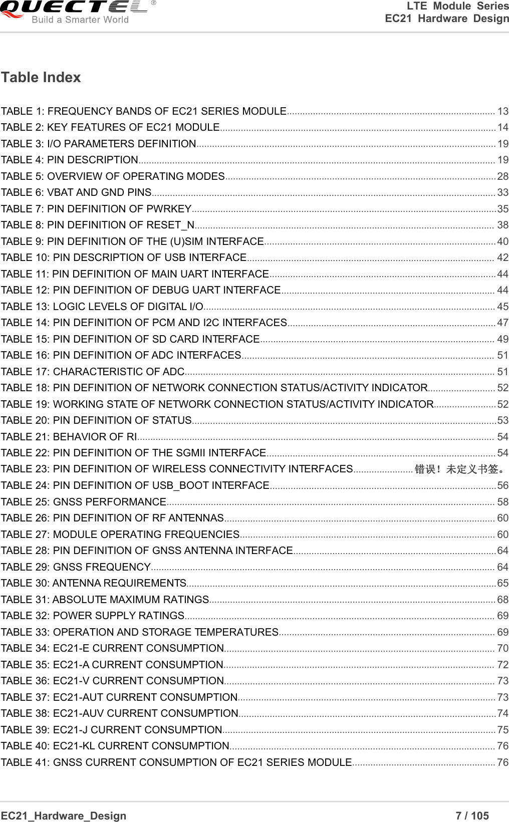
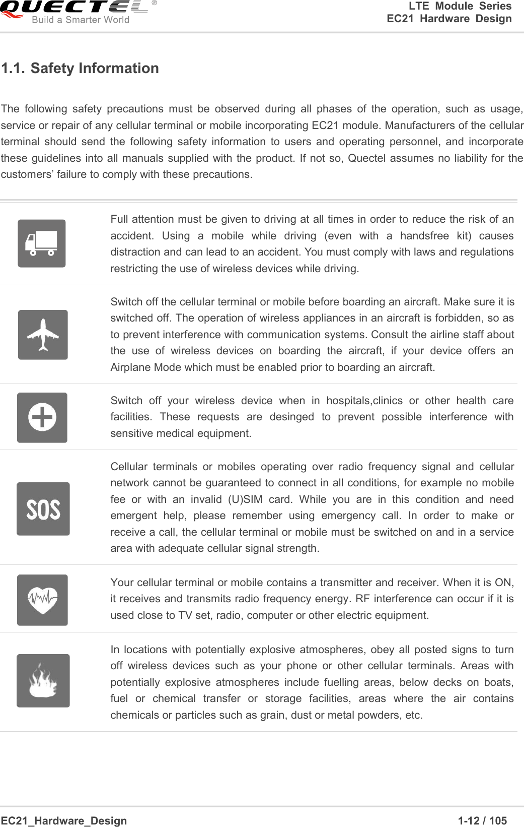
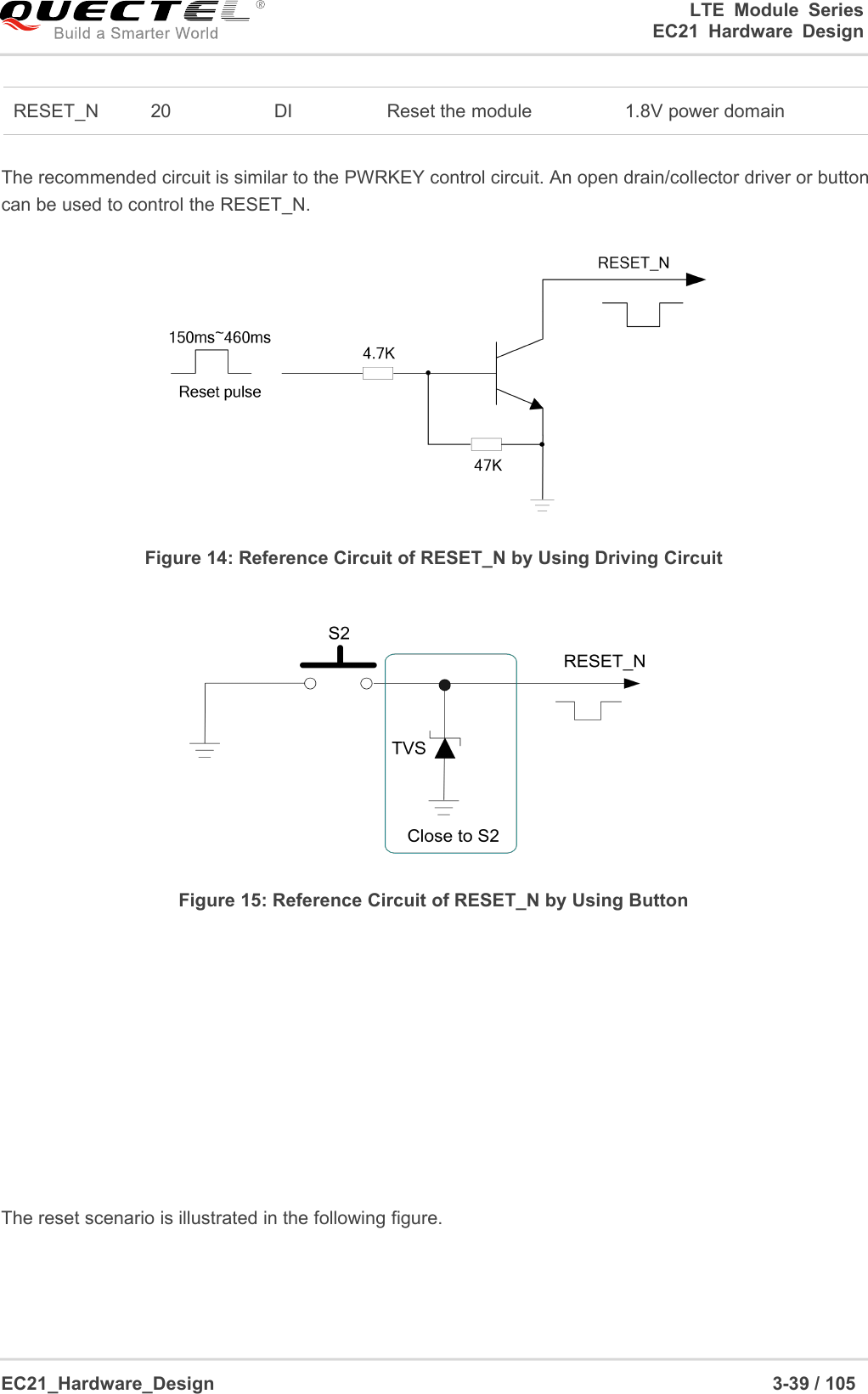
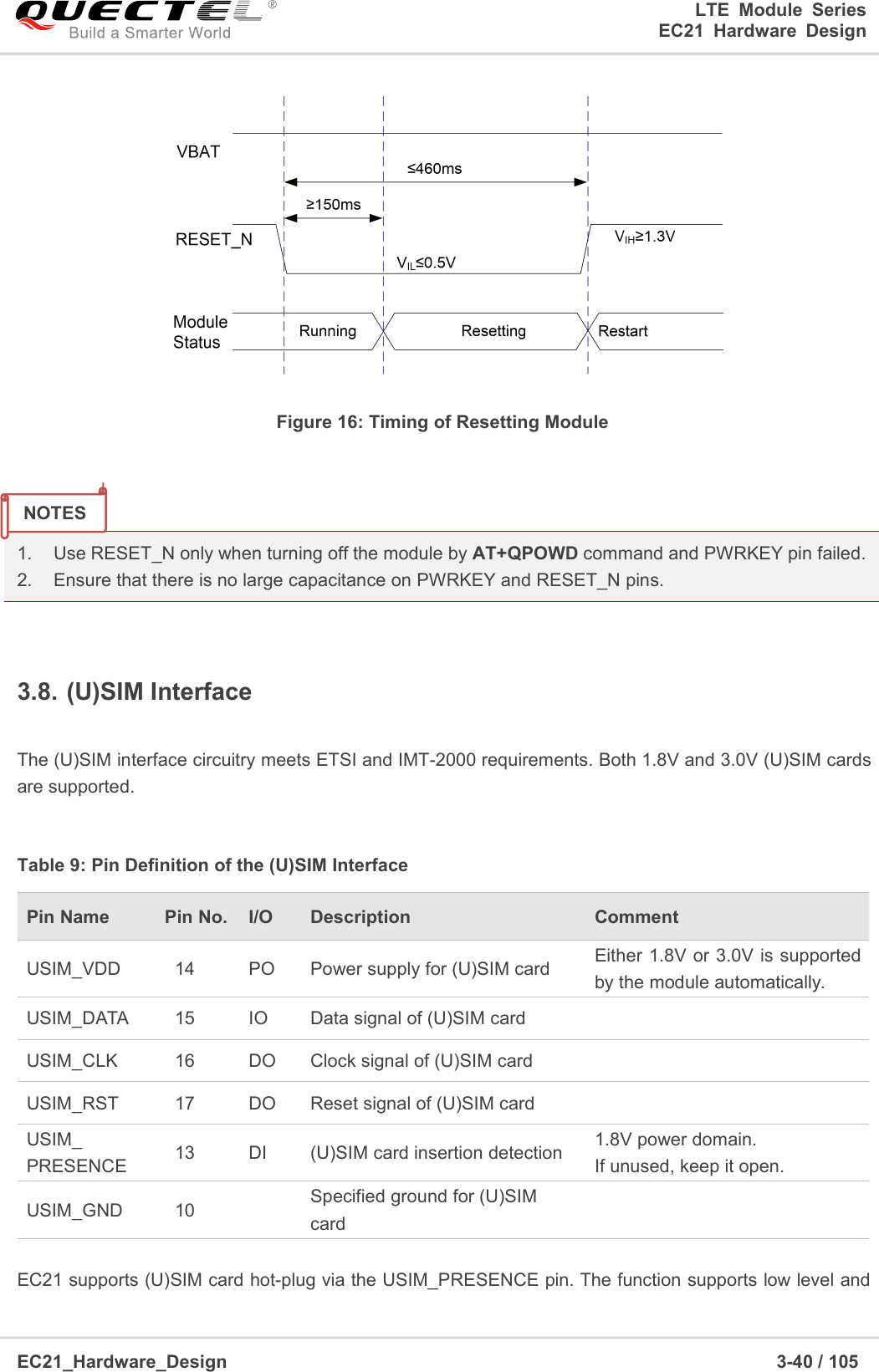
![LTE Module SeriesEC21 Hardware DesignEC21_Hardware_Design 3-38 / 105Figure 13: Timing of Turning off Module3.6.2.2. Turn off Module Using AT CommandIt is also a safe way to use AT+QPOWD command to turn off the module, which is similar to turning off themodule via PWRKEY pin.Please refer to document [2] for details about AT+QPOWD command.1. In order to avoid damaging internal flash, please do not switch off the power supply when the moduleworks normally. Only after the module is shut down by PWRKEY or AT command, the power supplycan be cut off.2. When turn off module with AT command, please keep PWRKEY at high level after the execution ofpower-off command. Otherwise the module will be turned on again after successfully turn-off.3.7. Reset the ModuleThe RESET_N pin can be used to reset the module. The module can be reset by driving RESET_N to alow level voltage for time between 150ms and 460ms.Table 8: Pin Definition of RESET_NPin NamePin No.I/ODescriptionCommentNOTE](https://usermanual.wiki/Quectel-Wireless-Solutions/201606EC21A/User-Guide-3885852-Page-39.png)
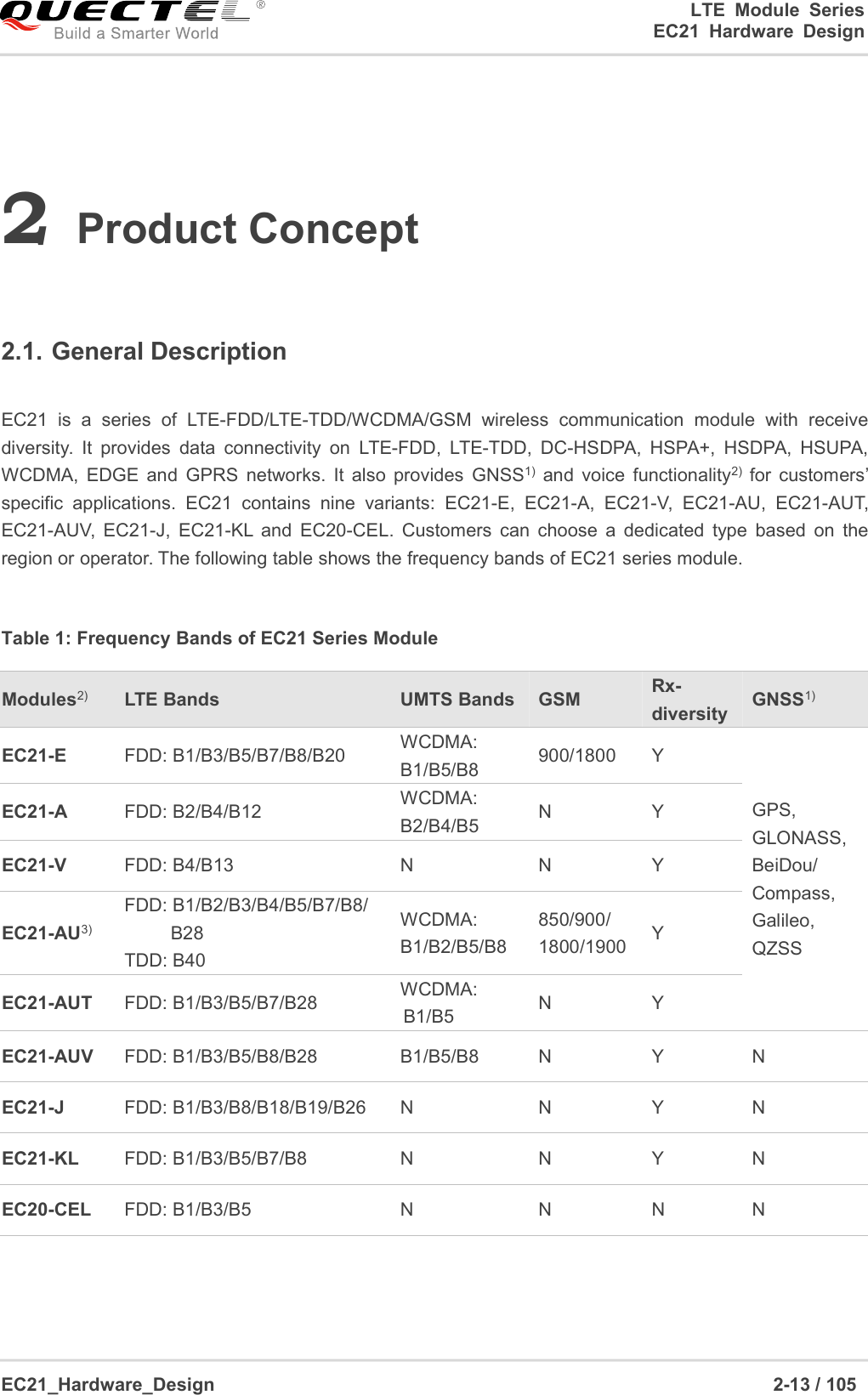
![LTE Module SeriesEC21 Hardware DesignEC21_Hardware_Design 3-41 / 105high level detections, and is disabled by default. Please refer to document [2] about AT+QSIMDETcommand for details.The following figure shows a reference design for (U)SIM interface with an 8-pin (U)SIM card connector.Figure 17: Reference Circuit of (U)SIM Interface with an 8-Pin (U)SIM Card ConnectorIf (U)SIM card detection function is not needed, please keep USIM_PRESENCE unconnected. Areference circuit for (U)SIM interface with a 6-pin (U)SIM card connector is illustrated in the followingfigure.Figure 18: Reference Circuit of (U)SIM Interface with a 6-Pin (U)SIM Card ConnectorIn order to enhance the reliability and availability of the (U)SIM card in customers’ applications, please](https://usermanual.wiki/Quectel-Wireless-Solutions/201606EC21A/User-Guide-3885852-Page-42.png)
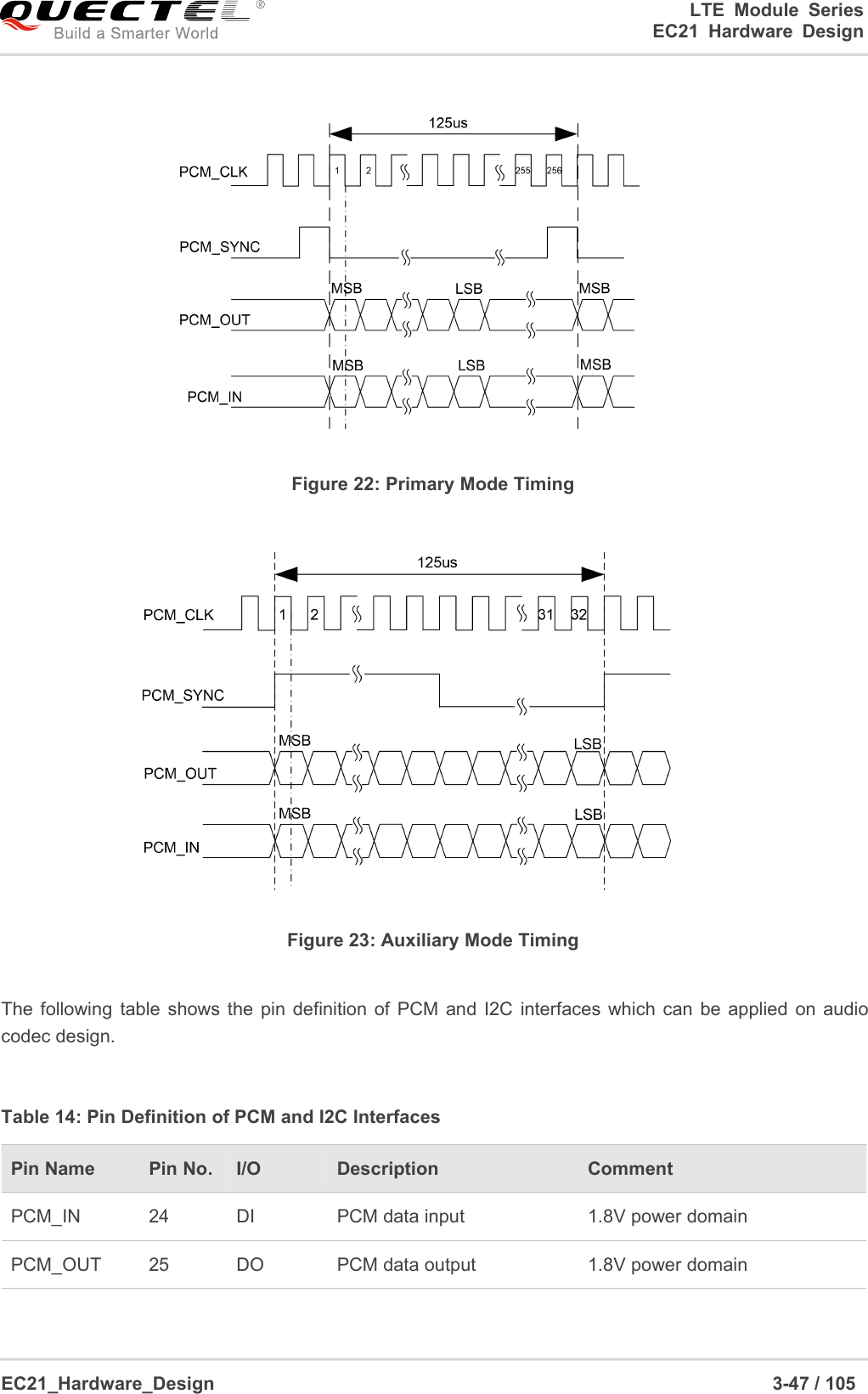
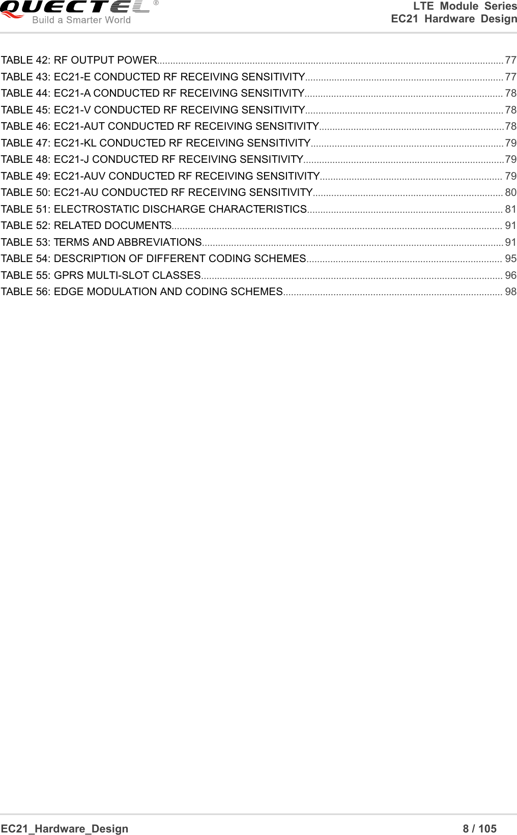
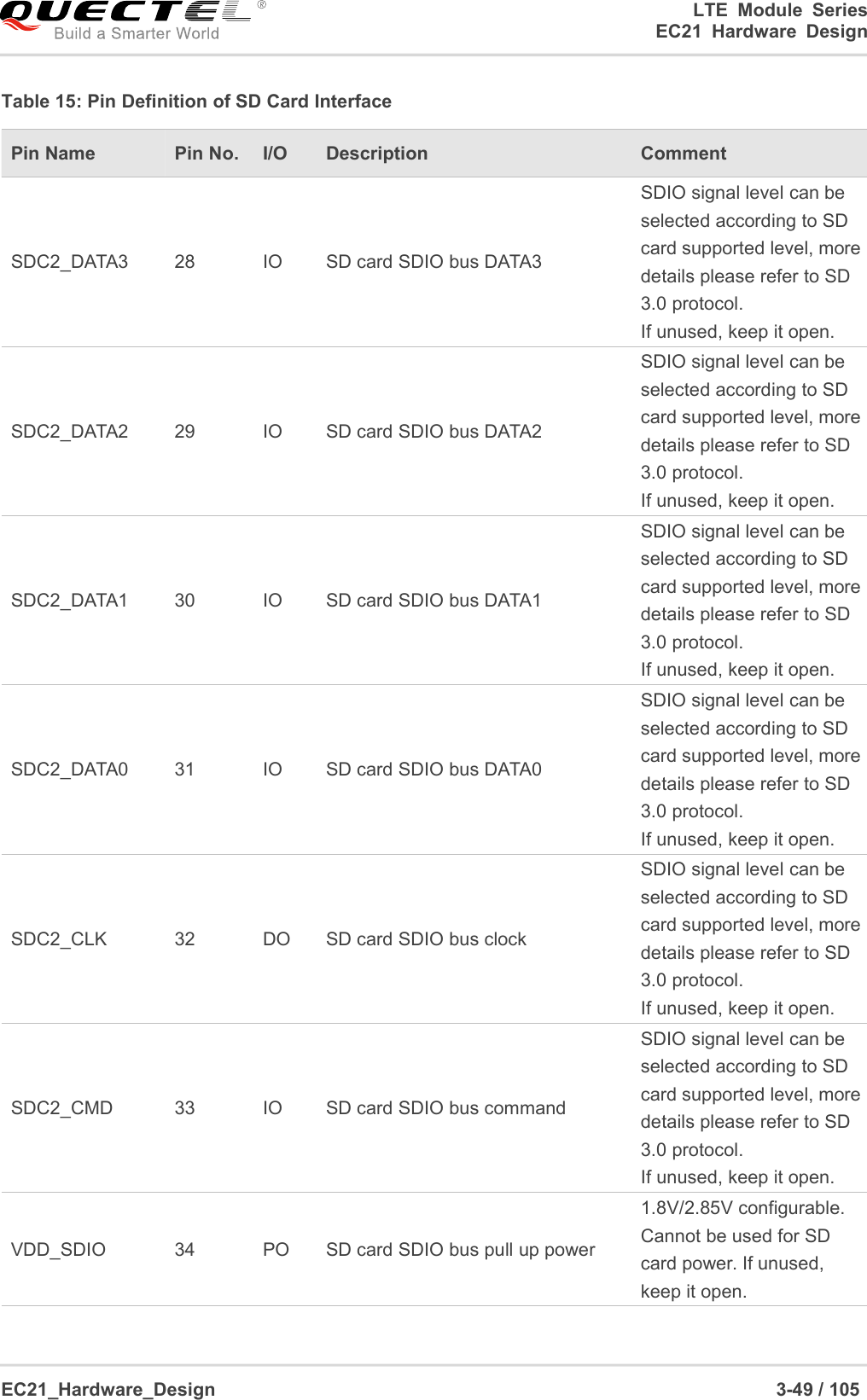
![LTE Module SeriesEC21 Hardware DesignEC21_Hardware_Design 3-48 / 105PCM_SYNC26IOPCM data framesynchronization signal1.8V power domainPCM_CLK27IOPCM data bit clock1.8V power domainI2C_SCL41ODI2C serial clockRequire external pull-up to 1.8VI2C_SDA42ODI2C serial dataRequire external pull-up to 1.8VClock and mode can be configured by AT command, and the default configuration is master mode usingshort frame synchronization format with 2048KHz PCM_CLK and 8KHz PCM_SYNC. Please refer todocument [2] about AT+QDAI command for details.The following figure shows a reference design of PCM interface with external codec IC.Figure 24: Reference Circuit of PCM Application with Audio Codec1. “*” means under development.2. It is recommended to reserve RC (R=22Ω, C=22pF) circuits on the PCM lines, especially forPCM_CLK.3. EC21 works as a master device pertaining to I2C interface.3.12. SD Card InterfaceEC21 supports SDIO3.0 interface for SD card.The following table shows the pin definition of SD card interface.NOTES](https://usermanual.wiki/Quectel-Wireless-Solutions/201606EC21A/User-Guide-3885852-Page-49.png)
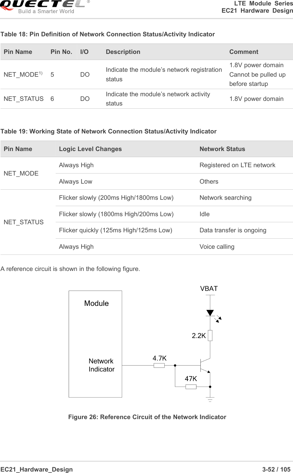
![LTE Module SeriesEC21 Hardware DesignEC21_Hardware_Design 3-51 / 1053.13. ADC InterfacesThe module provides two analog-to-digital converter (ADC) interfaces. AT+QADC=0 command can beused to read the voltage value on ADC0 pin. AT+QADC=1 command can be used to read the voltagevalue on ADC1 pin. For more details about these AT commands, please refer to document [2].In order to improve the accuracy of ADC, the trace of ADC should be surrounded by ground.Table 16: Pin Definition of ADC InterfacesPin NamePin No.DescriptionADC045General purpose analog to digital converterADC144General purpose analog to digital converterThe following table describes the characteristic of ADC function.Table 17: Characteristic of ADCParameterMin.Typ.Max.UnitADC0 Voltage Range0.3VBAT_BBVADC1 Voltage Range0.3VBAT_BBVADC Resolution15bits1. ADC input voltage must not exceed VBAT_BB.2. It is prohibited to supply any voltage to ADC pins when VBAT is removed.3. It is recommended to use a resistor divider circuit for ADC application.3.14. Network Status IndicationThe network indication pins can be used to drive network status indication LEDs. The module providestwo pins which are NET_MODE and NET_STATUS. The following tables describe the pin definition andlogic level changes in different network status.NOTES](https://usermanual.wiki/Quectel-Wireless-Solutions/201606EC21A/User-Guide-3885852-Page-52.png)
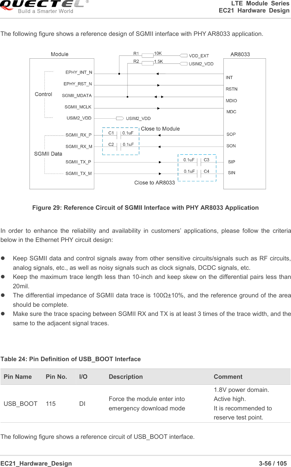
![LTE Module SeriesEC21 Hardware DesignEC21_Hardware_Design 3-54 / 105URC can be outputted from UART port, USB AT port and USB modem port through configuration viaAT+QURCCFG command. The default port is USB AT port.In addition, RI behavior can be configured flexibly. The default behavior of the RI is shown as below.Table 21: Behavior of RIStateResponseIdleRI keeps at high levelURCRI outputs 120ms low pulse when a new URC returnsThe RI behavior can be changed by AT+QCFG="urc/ri/ring" command. Please refer to document [2] fordetails.3.17. SGMII InterfaceEC21 includes an integrated Ethernet MAC with an SGMII interface and two management interfaces, keyfeatures of the SGMII interface are shown below:IEEE802.3 complianceSupport 10M/100M/1000M Ethernet work modeSupport VLAN taggingSupport IEEE1588 and Precision Time Protocol (PTP)Can be used to connect to external Ethernet PHY like AR8033, or to an external switchManagement interfaces support dual voltage 1.8V/2.85VThe following table shows the pin definition of SGMII interface.Table 22: Pin Definition of the SGMII InterfacePin NamePin No.I/ODescriptionCommentControl Signal PartEPHY_RST_N119DOEthernet PHY reset1.8V/2.85V power domainEPHY_INT_N120DIEthernet PHY interrupt1.8V power domainNOTE](https://usermanual.wiki/Quectel-Wireless-Solutions/201606EC21A/User-Guide-3885852-Page-55.png)
![LTE Module SeriesEC21 Hardware DesignEC21_Hardware_Design 4-58 / 1054GNSS Receiver4.1. General DescriptionEC21 includes a fully integrated global navigation satellite system solution that supports Gen8C-Lite ofQualcomm (GPS, GLONASS, BeiDou, Galileo and QZSS).EC21 supports standard NMEA-0183 protocol, and outputs NMEA sentences at 1Hz data update rate viaUSB interface by default.By default, EC21 GNSS engine is switched off. It has to be switched on via AT command. For more detailsabout GNSS engine technology and configurations, please refer to document [3].4.2. GNSS PerformanceThe following table shows the GNSS performance of EC21.Table 25: GNSS PerformanceParameterDescriptionConditionsTyp.UnitSensitivity(GNSS)Cold startAutonomous-146dBmReacquisitionAutonomous-157dBmTrackingAutonomous-157dBmTTFF(GNSS)Cold start@open skyAutonomous35sXTRA enabled18sWarm start@open skyAutonomous26sXTRA enabled2.2s](https://usermanual.wiki/Quectel-Wireless-Solutions/201606EC21A/User-Guide-3885852-Page-59.png)
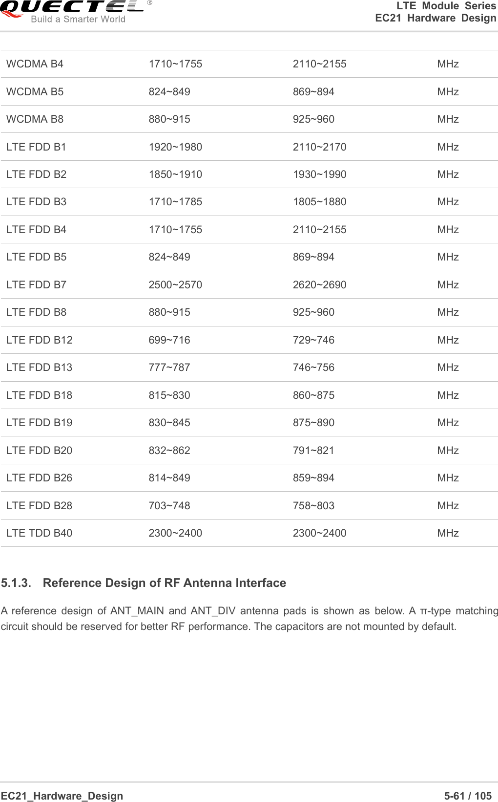
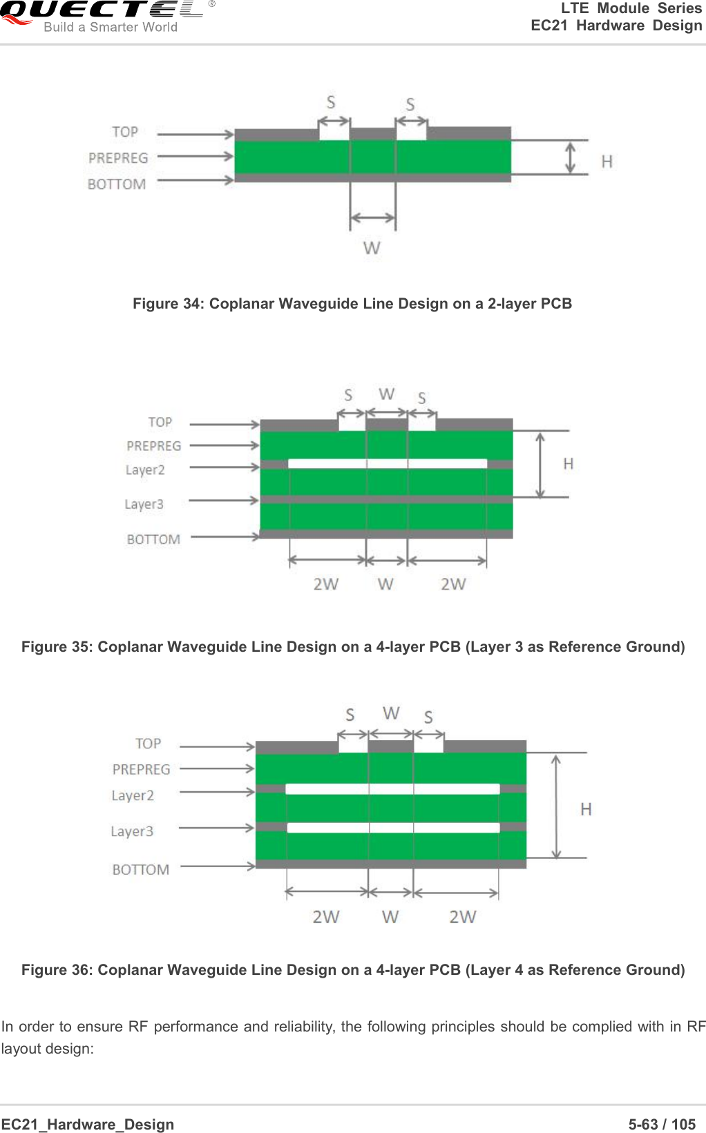
![LTE Module SeriesEC21 Hardware DesignEC21_Hardware_Design 5-64 / 105Use impedance simulation tool to control the characteristic impedance of RF traces as 50Ω.The GND pins adjacent to RF pins should not be designed as thermal relief pads, and should be fullyconnected to ground.The distance between the RF pins and the RF connector should be as short as possible, and all theright angle traces should be changed to curved ones.There should be clearance area under the signal pin of the antenna connector or solder joint.The reference ground of RF traces should be complete. Meanwhile, adding some ground vias aroundRF traces and the reference ground could help to improve RF performance. The distance betweenthe ground vias and RF traces should be no less than two times the width of RF signal traces (2*W).For more details about RF layout, please refer to document [6].5.2. GNSS Antenna InterfaceThe following tables show the pin definition and frequency specification of GNSS antenna interface.Table 28: Pin Definition of GNSS Antenna InterfacePin NamePin No.I/ODescriptionCommentANT_GNSS47AIGNSS antenna50Ω impedanceTable 29: GNSS FrequencyTypeFrequencyUnitGPS/Galileo/QZSS1575.42±1.023MHzGLONASS1597.5~1605.8MHzBeiDou1561.098±2.046MHz](https://usermanual.wiki/Quectel-Wireless-Solutions/201606EC21A/User-Guide-3885852-Page-65.png)
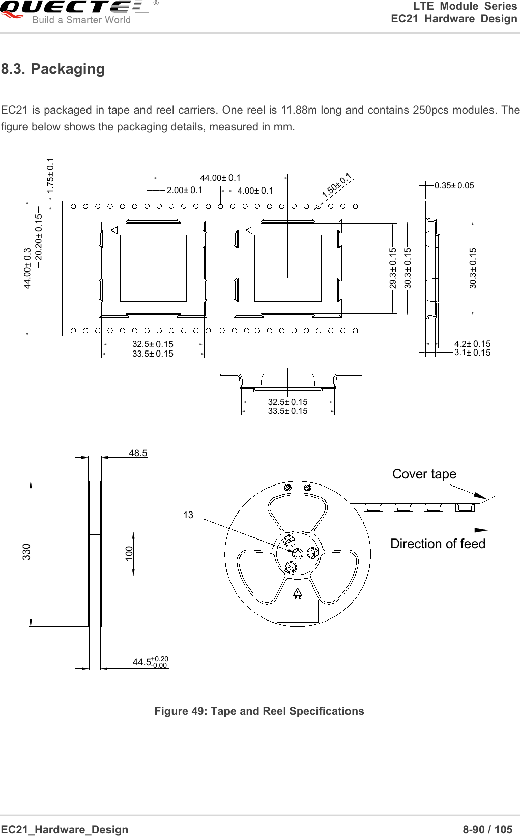
![LTE Module SeriesEC21 Hardware DesignEC21_Hardware_Design 8-89 / 1058.2. Manufacturing and SolderingPush the squeegee to apply the solder paste on the surface of stencil, thus making the paste fill thestencil openings and then penetrate to the PCB. The force on the squeegee should be adjusted properlyso as to produce a clean stencil surface on a single pass. To ensure the module soldering quality, thethickness of stencil for the module is recommended to be 0.20mm. For more details, please refer todocument [4].It is suggested that the peak reflow temperature is 235ºC~245ºC (for SnAg3.0Cu0.5 alloy). The absolutemaximum reflow temperature is 260ºC. To avoid damage to the module caused by repeated heating, it issuggested that the module should be mounted after reflow soldering for the other side of PCB has beencompleted. Recommended reflow soldering thermal profile is shown below:Figure 48: Reflow Soldering Thermal ProfileDuring manufacturing and soldering, or any other processes that may contact the module directly, NEVERwipe the module label with organic solvents, such as acetone, ethyl alcohol, isopropyl alcohol,trichloroethylene, etc.NOTE](https://usermanual.wiki/Quectel-Wireless-Solutions/201606EC21A/User-Guide-3885852-Page-90.png)
![LTE Module SeriesEC21 Hardware DesignEC21_Hardware_Design 9-91 / 1059Appendix A ReferencesTable 52: Related DocumentsSNDocument NameRemark[1]Quectel_EC2x&EG9x&EM05_Power_Management_Application_NotePower management application noteforEC25, EC21, EC20 R2.0, EC20 R2.1,EG95, EG91 and EM05 modules[2]Quectel_EC25&EC21_AT_Commands_ManualEC25 and EC21 AT commands manual[3]Quectel_EC25&EC21_GNSS_AT_Commands_ManualEC25 and EC21 GNSS AT commandsmanual[4]Quectel_Module_Secondary_SMT_User_GuideModule secondary SMT user guide[5]Quectel_EC21_Reference_DesignEC21 reference design[6]Quectel_RF_Layout_Application_NoteRF layout application noteTable 53: Terms and AbbreviationsAbbreviationDescriptionAMRAdaptive Multi-ratebpsBits Per SecondCHAPChallenge Handshake Authentication ProtocolCSCoding SchemeCSDCircuit Switched DataCTSClear To SendDC-HSPA+Dual-carrier High Speed Packet AccessDFOTADelta Firmware Upgrade Over The AirDLDownlink](https://usermanual.wiki/Quectel-Wireless-Solutions/201606EC21A/User-Guide-3885852-Page-92.png)