Quectel Wireless Solutions 201607EC25V LTE Module User Manual
Quectel Wireless Solutions Company Limited LTE Module Users Manual
UserManual.wiki
>
Quectel Wireless Solutions
>
201607EC25V User Manual
>
Users Manual
Contents
1.
User Manual
2.
User manual
3.
Users Manual
4.
User Manual -statement
Users Manual
Navigation menu
Upload a User Manual
Namespaces
Wiki Guide
HTML
PDF
Info
Views
User Manual
Discussion / Help
Navigation
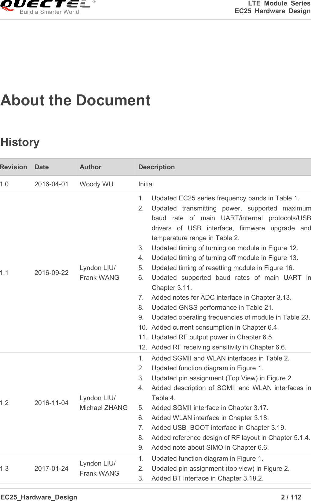
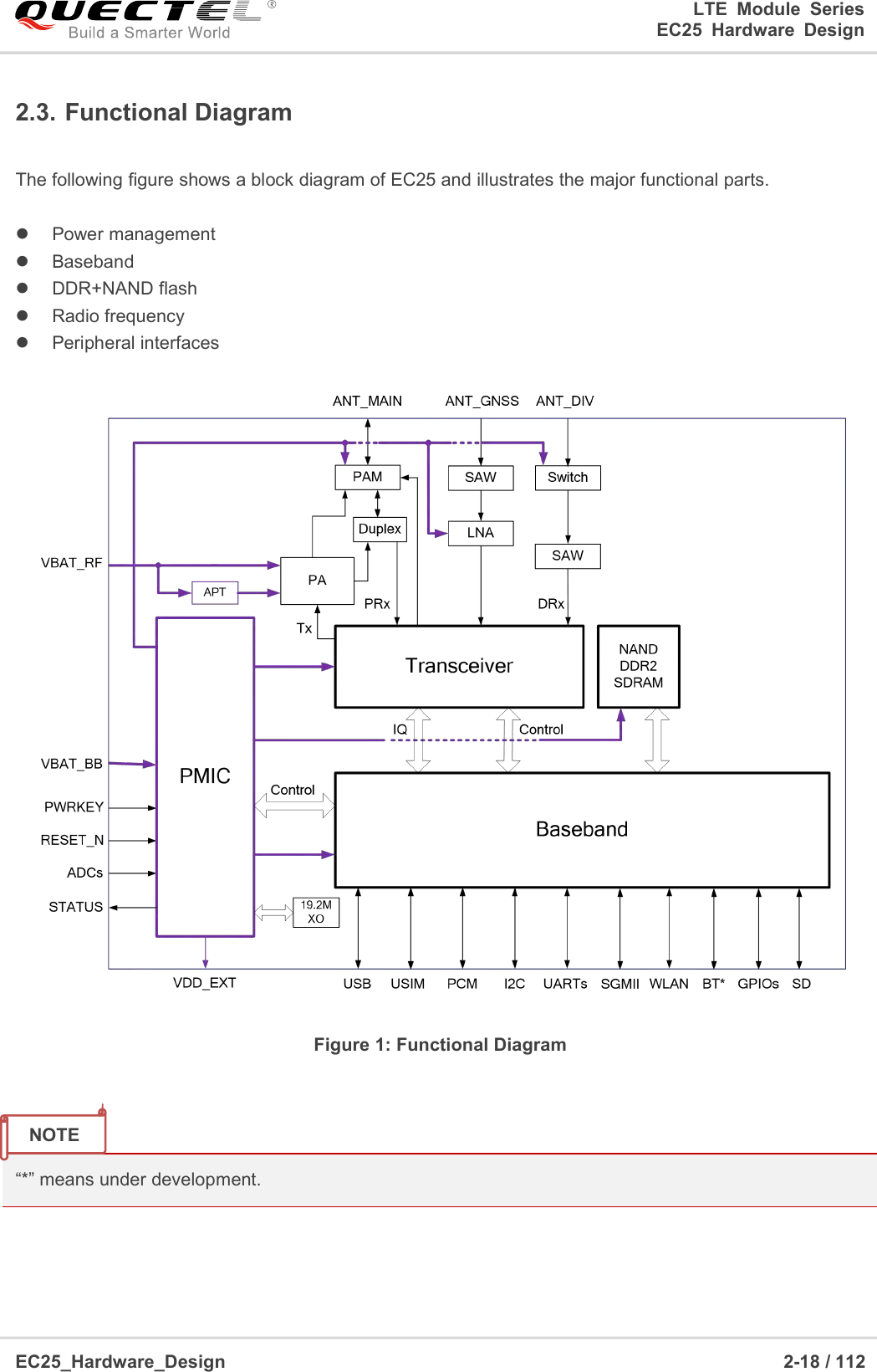
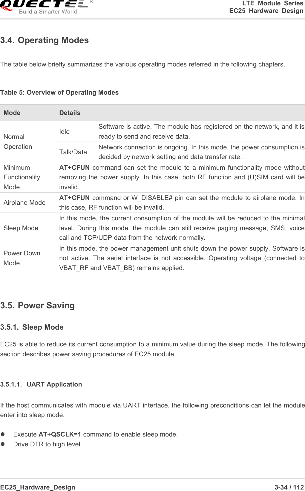
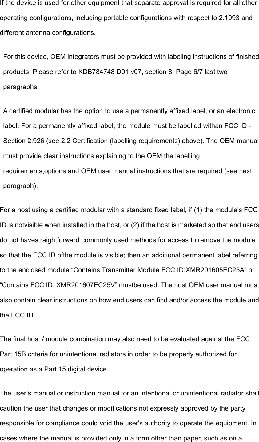
![LTE Module SeriesEC25 Hardware DesignEC25_Hardware_Design 3-37 / 112Sending data to EC25 through USB will wake up the module.When EC25 has a URC to report, RI signal will wake up the host.3.5.1.4. USB Application without USB Suspend FunctionIf the host does not support USB suspend function, USB_VBUS should be disconnected via an additionalcontrol circuit to let the module enter into sleep mode.Execute AT+QSCLK=1 command to enable sleep mode.Ensure the DTR is held at high level or keep it open.Disconnect USB_VBUS.The following figure shows the connection between the module and the host.Figure 6: Sleep Mode Application without Suspend FunctionSwitching on the power switch to supply power to USB_VBUS will wake up the module.Please pay attention to the level match shown in dotted line between the module and the host. For moredetails about EC25 power management application, please refer to document [1].3.5.2. Airplane ModeWhen the module enters into airplane mode, the RF function does not work, and all AT commandscorrelative with RF function will be inaccessible. This mode can be set via the following ways.NOTE](https://usermanual.wiki/Quectel-Wireless-Solutions/201607EC25V.Users-Manual/User-Guide-3970452-Page-38.png)
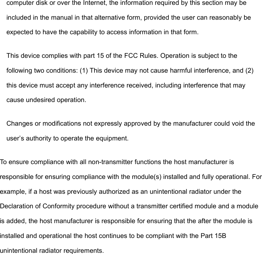
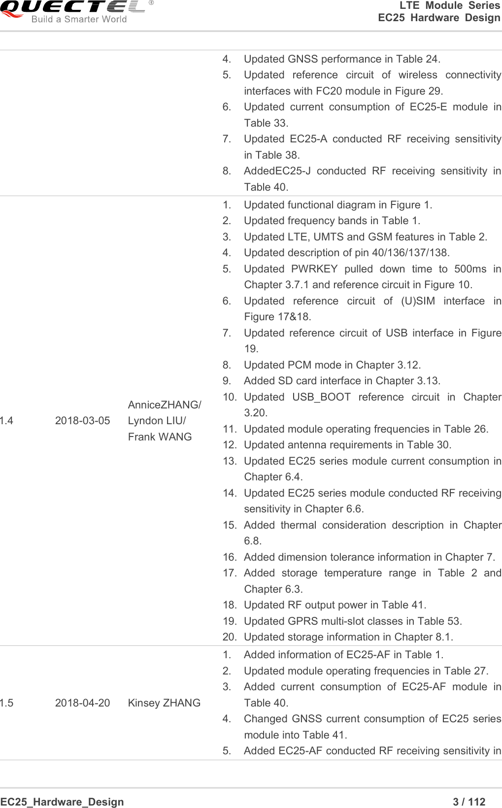
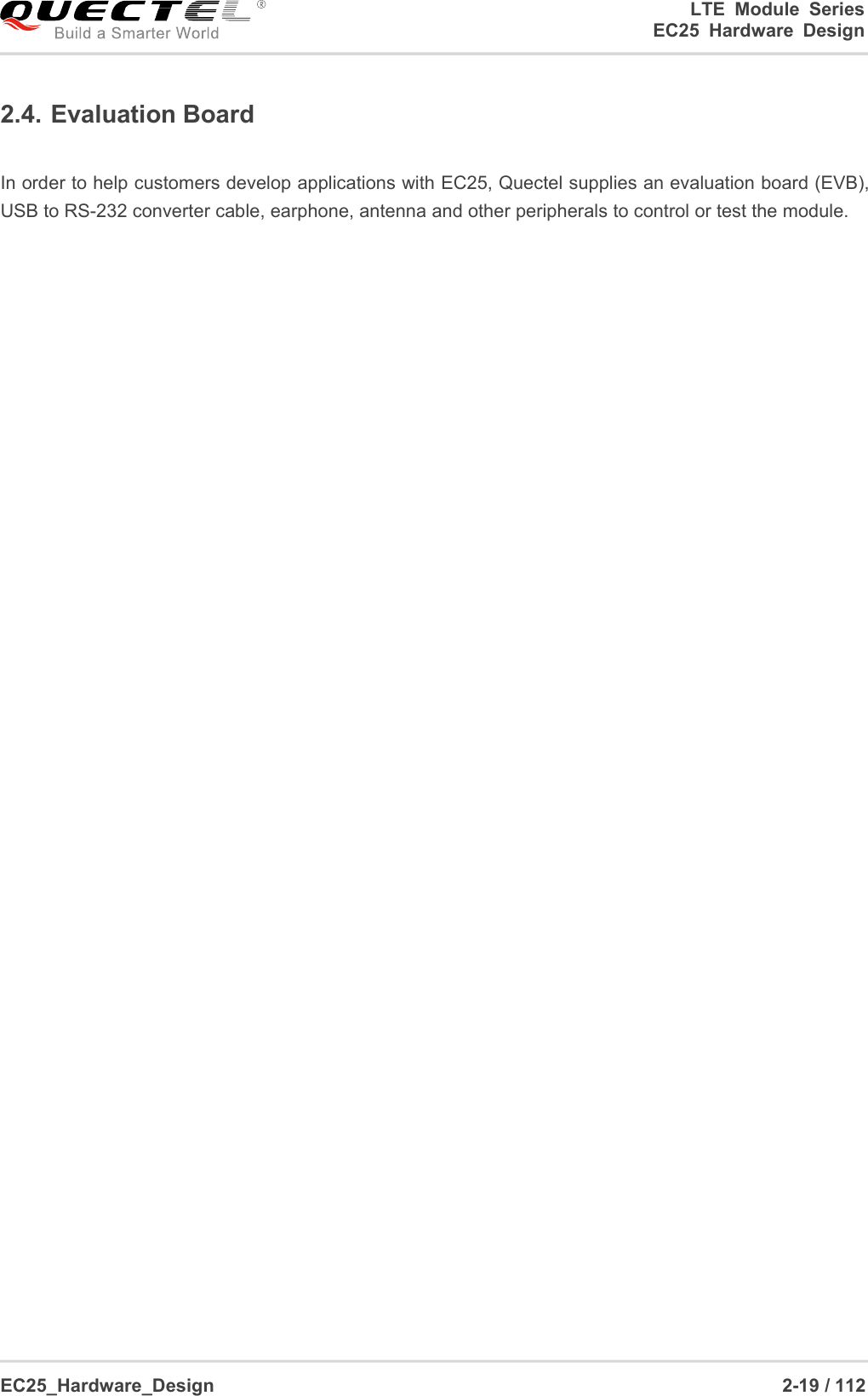
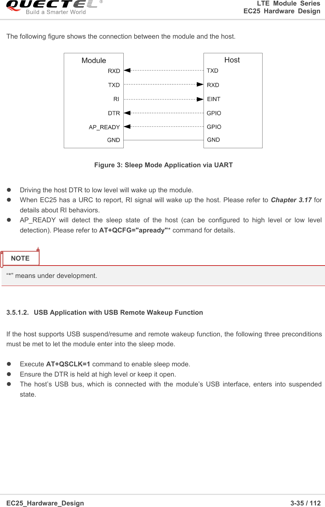
![LTE Module SeriesEC25 Hardware DesignEC25_Hardware_Design 3-40 / 1123.6.3. Reference Design for Power SupplyPower design for the module is very important, as the performance of the module largely depends on thepower source. The power supply should be able to provide sufficient current up to 2A at least. If thevoltage drop between the input and output is not too high, it is suggested that an LDO should be used tosupply power for the module. If there is a big voltage difference between the input source and the desiredoutput (VBAT), a buck converter is preferred to be used as the power supply.The following figure shows a reference design for +5V input power source. The typical output of the powersupplyis about 3.8V and the maximum load current is 3A.Figure 9: Reference Circuit of Power SupplyIn order to avoid damaging internal flash, please do not switch off the power supply when the moduleworks normally. Only after the module is shutdown by PWRKEY or AT command, then the power supplycan be cut off.3.6.4. Monitor the Power SupplyAT+CBC command can be used to monitor the VBAT_BB voltage value. For more details, please refer todocument [2].3.7. Turn on and off Scenarios3.7.1. Turn on Module Using the PWRKEYThe following table shows the pin definition of PWRKEY.NOTE](https://usermanual.wiki/Quectel-Wireless-Solutions/201607EC25V.Users-Manual/User-Guide-3970452-Page-41.png)
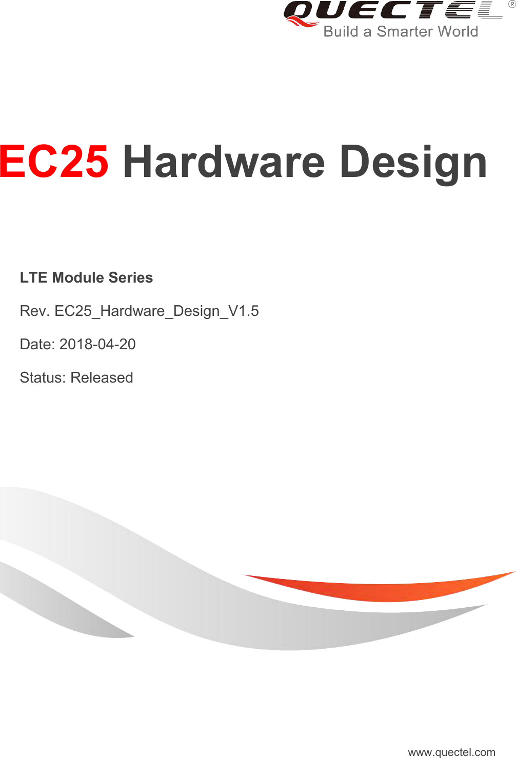
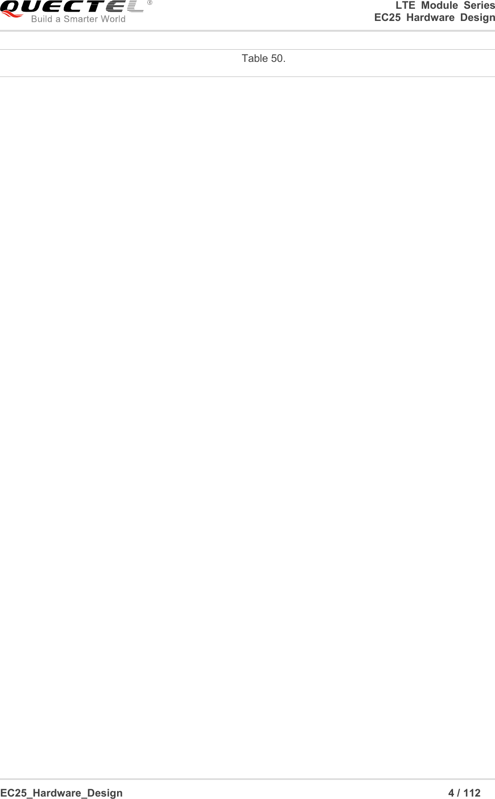
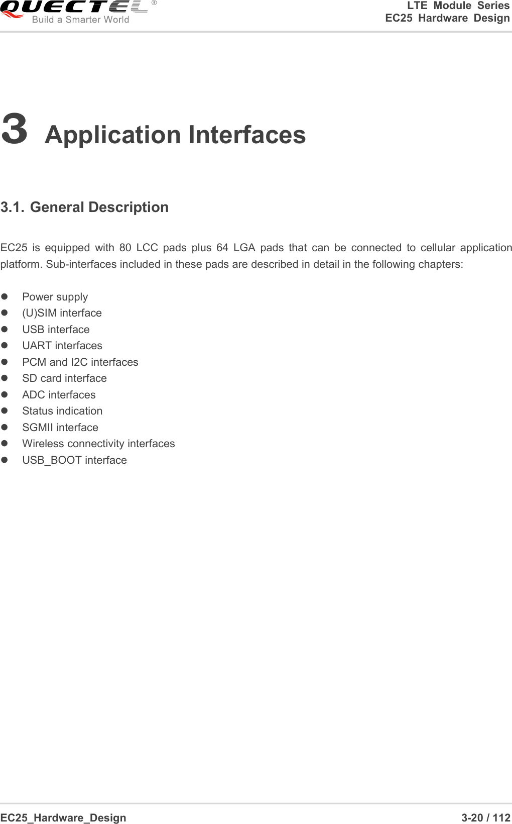
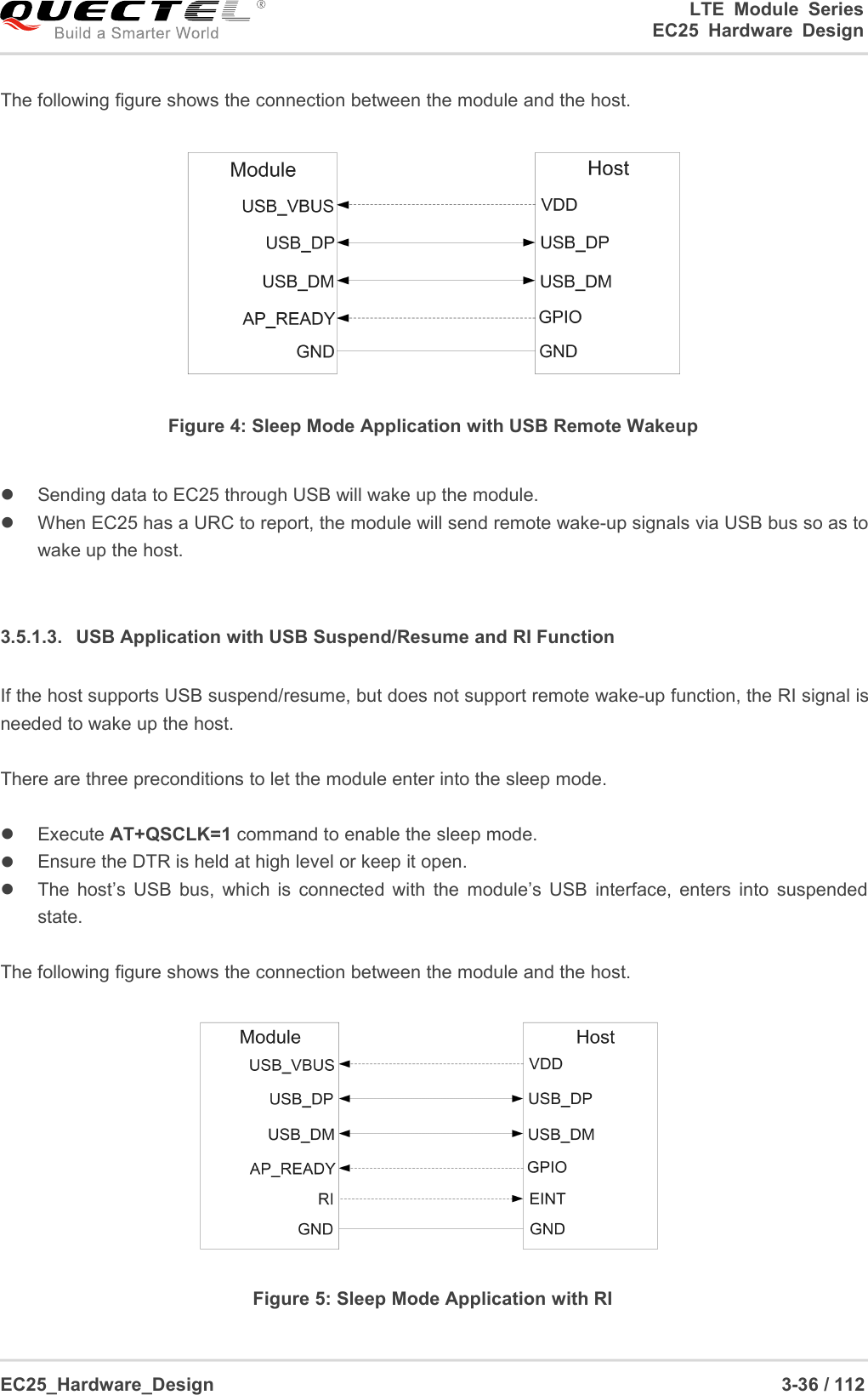
![LTE Module SeriesEC25 Hardware DesignEC25_Hardware_Design 3-43 / 112Figure 13: Timing of Turning off Module3.7.2.2. Turn off Module Using AT CommandIt is also a safe way to use AT+QPOWD command to turn off the module, which is similar to turning off themodule via PWRKEY pin.Please refer to document [2] for details about AT+QPOWD command.1. Inorder to avoid damaging internal flash, please do not switch off the power supply when the moduleworks normally. Only after the module is shut down by PWRKEY or AT command, then the powersupply can be cut off.2. When turn off module with AT command, please keep PWRKEY at high level after the execution ofpower-off command. Otherwise the module will be turned on again after successfully turn-off.3.8. Reset the ModuleThe RESET_N pin can be used to reset the module. The module can be reset by driving RESET_N to alow level voltage for time between 150ms and 460ms.Table 8: RESET_N Pin DescriptionPin NamePin No.I/ODescriptionCommentRESET_N20DIReset the module1.8V power domainNOTES](https://usermanual.wiki/Quectel-Wireless-Solutions/201607EC25V.Users-Manual/User-Guide-3970452-Page-44.png)
![LTE Module SeriesEC25 Hardware DesignEC25_Hardware_Design 3-45 / 1121. Use RESET_N only when turning off the module by AT+QPOWD command and PWRKEY pin failed.2. Ensure that there is no large capacitance on PWRKEY and RESET_N pins.3.9. (U)SIM InterfaceThe(U)SIM interface circuitry meets ETSI and IMT-2000 requirements. Both 1.8V and 3.0V (U)SIM cardsare supported.Table 9: Pin Definition of the (U)SIM InterfaceEC25 supports (U)SIM card hot-plug via the USIM_PRESENCE pin. The function supports low level andhigh level detections, and it is disabled by default. Please refer to document [2] for more details aboutAT+QSIMDET command.Pin NamePin No.I/ODescriptionCommentUSIM_VDD14POPower supply for (U)SIM cardEither 1.8V or 3.0V is supportedby the module automatically.USIM_DATA15IOData signal of (U)SIM cardUSIM_CLK16DOClock signal of (U)SIM cardUSIM_RST17DOReset signal of (U)SIM cardUSIM_PRESENCE13DI(U)SIM card insertion detectionUSIM_GND10Specified ground for (U)SIM cardNOTES](https://usermanual.wiki/Quectel-Wireless-Solutions/201607EC25V.Users-Manual/User-Guide-3970452-Page-46.png)
![LTE Module SeriesEC25 Hardware DesignEC25_Hardware_Design 3-53 / 112Clock and mode can be configured by AT command, and the default configuration is master mode usingshort frame synchronization format with 2048KHz PCM_CLK and 8KHz PCM_SYNC. Please refer todocument [2] for more details about AT+QDAI command.The following figure shows a reference design of PCM interface with external codec IC.Figure 24: Reference Circuit of PCM Application with Audio Codec1. It is recommended to reserve an RC (R=22Ω, C=22pF) circuits on the PCM lines, especially forPCM_CLK.2. EC25 works as a master device pertaining to I2C interface.3.13. SD Card InterfaceEC25 supports SDIO 3.0 interface for SD card.PCM_SYNC26IOPCM data framesynchronization signal1.8V power domainPCM_CLK27IOPCM data bit clock1.8V power domainI2C_SCL41ODI2C serial clockRequire external pull-up to 1.8VI2C_SDA42ODI2C serial dataRequire external pull-up to 1.8VNOTES](https://usermanual.wiki/Quectel-Wireless-Solutions/201607EC25V.Users-Manual/User-Guide-3970452-Page-54.png)
![LTE Module SeriesEC25 Hardware DesignEC25_Hardware_Design 3-56 / 112Make sure the adjacent trace spacing is two times of the trace width and the load capacitance ofSDIO bus should be less than 15pF.It is recommended to keep the trace length difference between CLK and DATA/CMD less than 1mmand the total routing length less than 50mm. The total trace length inside the module is 27mm, so theexterior total trace length should be less than 23mm.3.14. ADC InterfacesThe module provides two analog-to-digital converter (ADC) interfaces. AT+QADC=0 command can beused to read the voltage value on ADC0 pin. AT+QADC=1 command can be used to read the voltagevalue on ADC1 pin. For more details about these AT commands, please refer to document [2].In order to improve the accuracy of ADC, the trace of ADC should be surrounded by ground.Table 16: Pin Definition of ADC InterfacesThe following table describes the characteristic of ADC function.Table 17: Characteristic of ADC1. ADC input voltage must not exceed VBAT_BB.2. It is prohibited to supply any voltage to ADC pins when VBAT is removed.Pin NamePin No.DescriptionADC045General purpose analog to digital converterADC144General purpose analog to digital converterParameterMin.Typ.Max.UnitADC0 Voltage Range0.3VBAT_BBVADC1 Voltage Range0.3VBAT_BBVADC Resolution15BitsNOTES](https://usermanual.wiki/Quectel-Wireless-Solutions/201607EC25V.Users-Manual/User-Guide-3970452-Page-57.png)
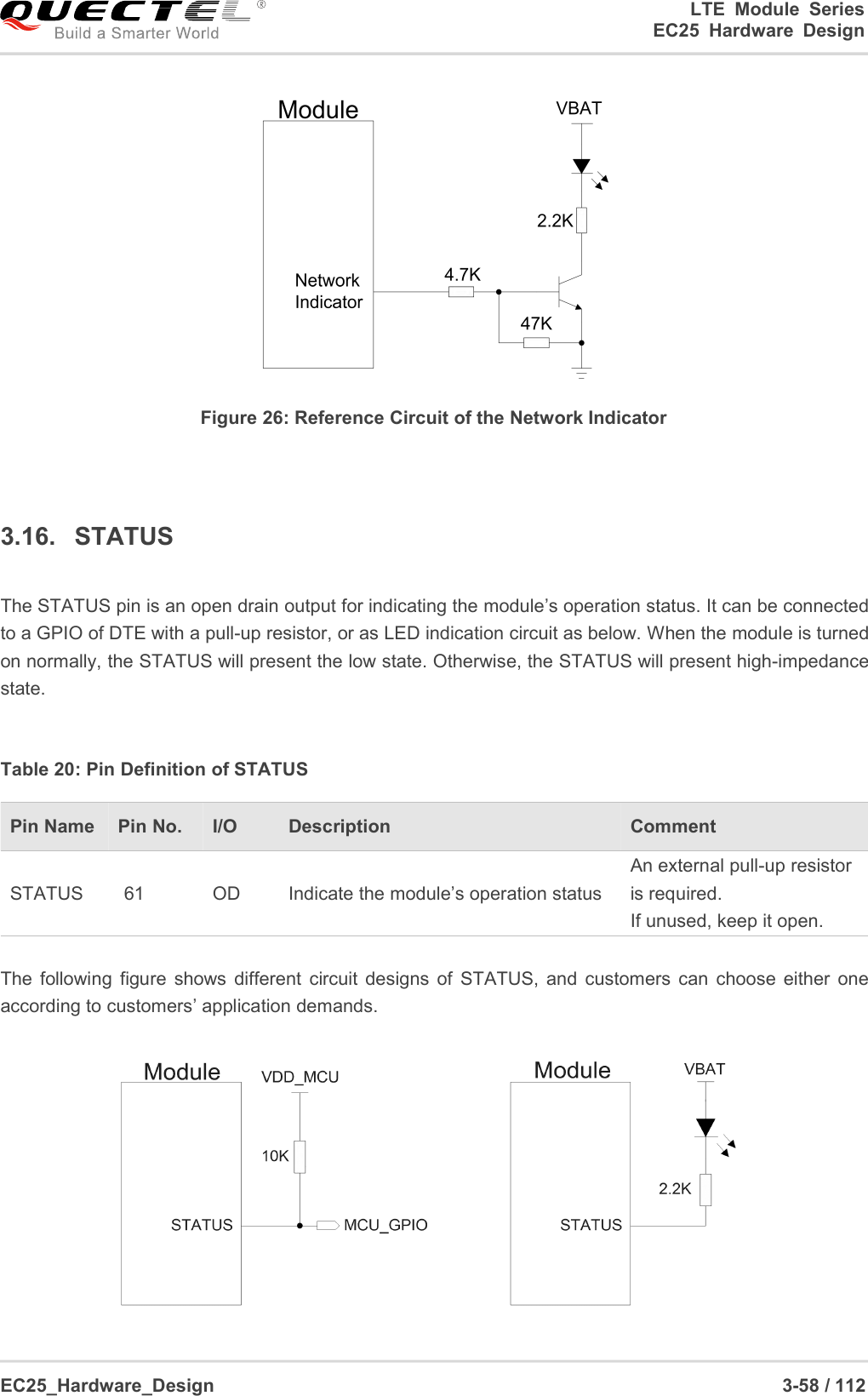
![LTE Module SeriesEC25 Hardware DesignEC25_Hardware_Design 3-59 / 112Figure 27: Reference Circuits of STATUS3.17. Behaviors of RIAT+QCFG="risignaltype","physical" command can be used to configure RI behavior.No matter on which port URC is presented, URC will trigger the behavior of RI pin.URC can be outputted from UART port, USB AT port and USB modem port through configuration viaAT+QURCCFG command. The default port is USB AT port.In addition, RI behavior can be configured flexibly. The default behavior of the RI is shown as below.Table 21: Behavior of RIThe RI behavior can be changed by AT+QCFG="urc/ri/ring" command. Please refer to document [2]for details.3.18. SGMII InterfaceEC25 includes an integrated Ethernet MAC with an SGMII interface and two management interfaces, keyfeatures of the SGMII interface are shown below:IEEE802.3 complianceSupport 10M/100M/1000M Ethernet work modeSupport maximum 150Mbps (DL)/50Mbps (UL) for 4G networkSupport VLAN taggingSupport IEEE1588 and Precision Time Protocol (PTP)Can be used to connect to external Ethernet PHY like AR8033, or to an external switchStateResponseIdleRI keeps at high levelURCRI outputs 120ms low pulse when a new URC returnsNOTE](https://usermanual.wiki/Quectel-Wireless-Solutions/201607EC25V.Users-Manual/User-Guide-3970452-Page-60.png)
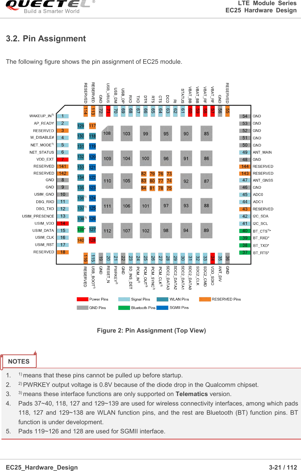
![LTE Module SeriesEC25 Hardware DesignEC25_Hardware_Design 3-63 / 112The following figure shows a reference design of wireless connectivity interfaces with Quectel FC20module.Figure 30: Reference Circuit of Wireless Connectivity Interfaces with FC20 Module1. FC20 module can only be used as a slave device.2. When BT function is enabled on EC25 module, PCM_SYNC and PCM_CLK pins are only used tooutput signals.3. For more information about wireless connectivity interfaces, please refer to document [5].4. “*” means under development.5. 1) Pads 24~27 are multiplexing pins used for audio design on EC25 module and BT function on BTmodule.3.19.1. WLAN InterfaceEC25 provides a low power SDIO 3.0 interface and control interface for WLAN design.SDIO interface supports the SDR mode (up to 50MHz).As SDIO signals are very high-speed, in order to ensure the SDIO interface design corresponds with theBT_EN*139DOBT function control via BT module.1.8V power domainActive high.NOTES](https://usermanual.wiki/Quectel-Wireless-Solutions/201607EC25V.Users-Manual/User-Guide-3970452-Page-64.png)
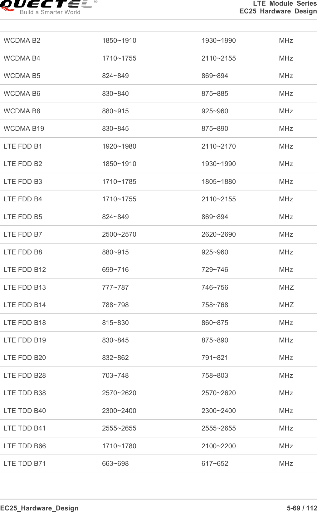
![LTE Module SeriesEC25 Hardware DesignEC25_Hardware_Design 4-66 / 1124GNSS Receiver4.1. General DescriptionEC25 includes a fully integrated global navigation satellite system solution that supports Gen8C-Lite ofQualcomm (GPS, GLONASS, BeiDou, Galileo and QZSS).EC25 supports standard NMEA-0183 protocol, and outputs NMEA sentences at 1Hz data update rate viaUSB interface by default.By default, EC25 GNSS engine is switched off. It has to be switched on via AT command. For moredetails about GNSS engine technology and configurations, please refer to document [3].4.2. GNSS PerformanceThe following table shows GNSS performance of EC25.Table 25: GNSS PerformanceParameterDescriptionConditionsTyp.UnitSensitivity(GNSS)Cold startAutonomous-146dBmReacquisitionAutonomous-157dBmTrackingAutonomous-157dBmTTFF(GNSS)Cold start@open skyAutonomous35sXTRA enabled18sWarm start@open skyAutonomous26sXTRA enabled2.2sHot startAutonomous2.5s](https://usermanual.wiki/Quectel-Wireless-Solutions/201607EC25V.Users-Manual/User-Guide-3970452-Page-67.png)
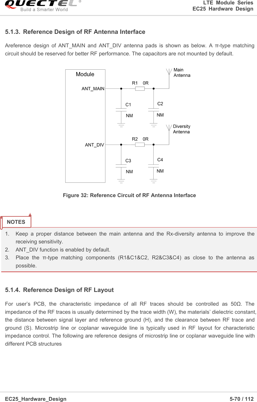
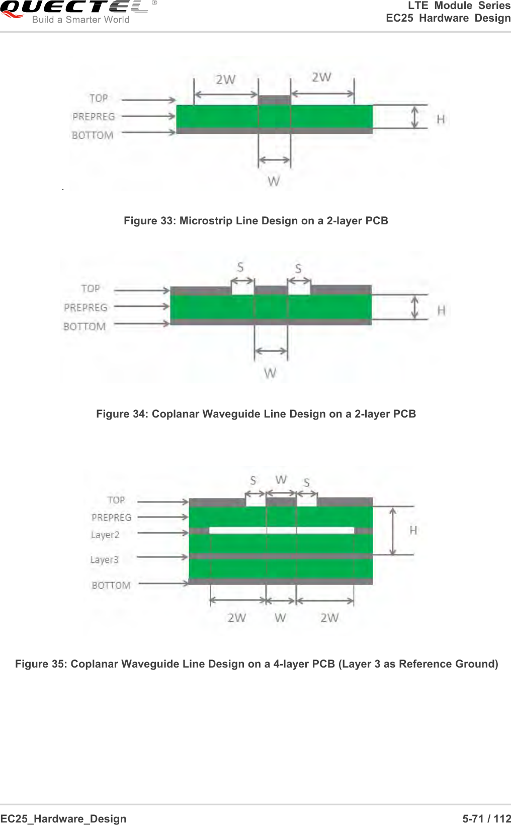
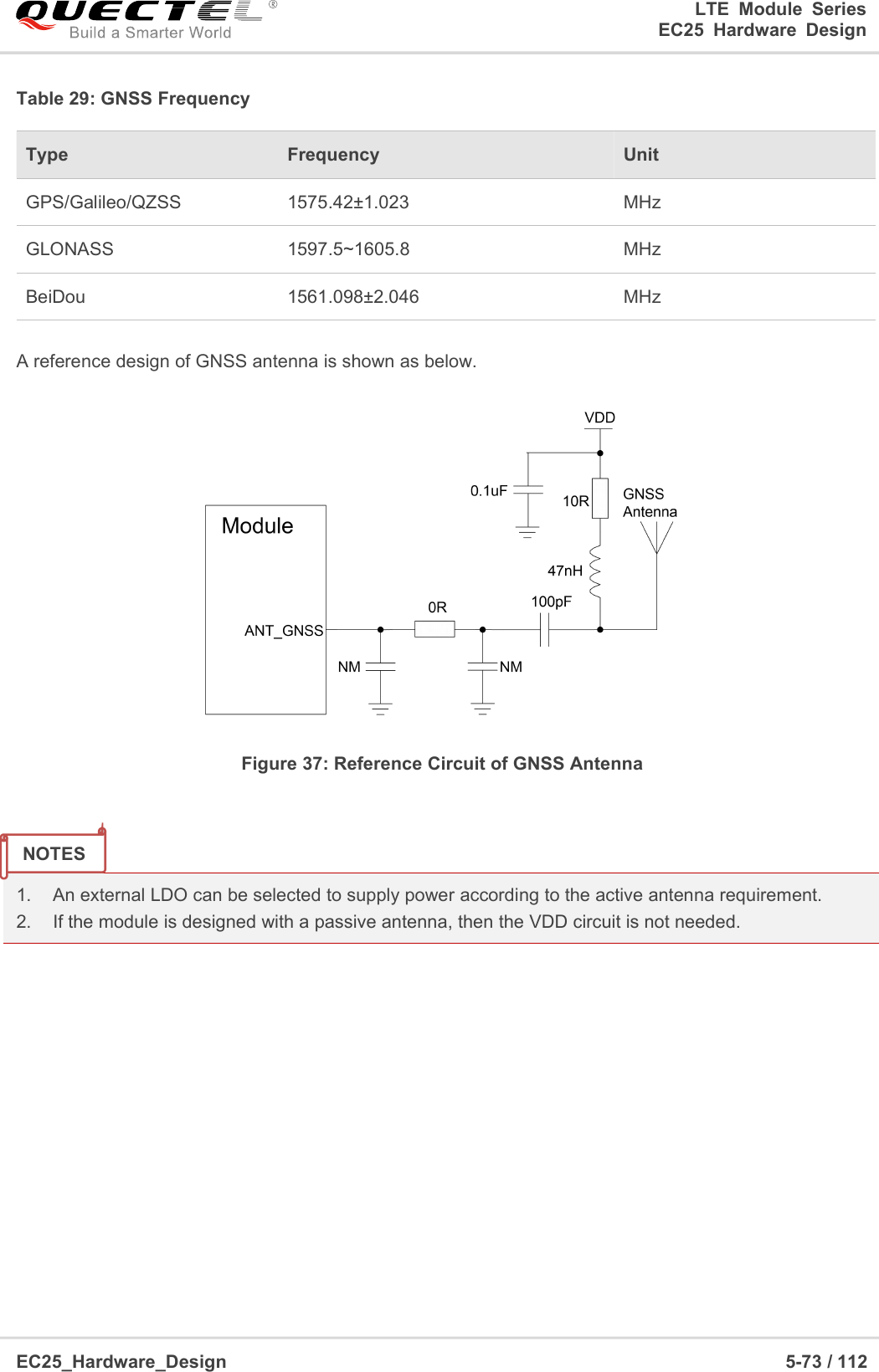
![LTE Module SeriesEC25 Hardware DesignEC25_Hardware_Design 5-72 / 112Figure 36: Coplanar Waveguide Line Design on a 4-layer PCB (Layer 4 as Reference Ground)In order to ensure RF performance and reliability, the following principles should be complied with in RFlayout design:Please use an impedance simulation tool to control the characteristic impedance of RF traces as50Ω.The GND pins adjacent to RF pins should not be designed as thermal relief pads, and they should befully connected to ground.The distance between the RF pins and the RF connector should be as short as possible, and all theright angle traces should be changed to curved ones.There should be clearance area under the signal pin of the antenna connector or solder joint.The reference ground of RF traces should be complete. Meanwhile, adding some ground vias aroundRF traces and the reference ground could help to improve RF performance. The distance betweenthe ground vias and RF traces should be no less than two times the width of RF signal traces (2*W).For more details about RF layout, please refer to document [6].5.2. GNSS Antenna InterfaceThe following tables show pin definition and frequency specification of GNSS antenna interface.Table 28: Pin Definition of GNSS Antenna InterfacePin NamePin No.I/ODescriptionCommentANT_GNSS47AIGNSS antenna50Ω impedanceIf unused, keep it open.](https://usermanual.wiki/Quectel-Wireless-Solutions/201607EC25V.Users-Manual/User-Guide-3970452-Page-73.png)
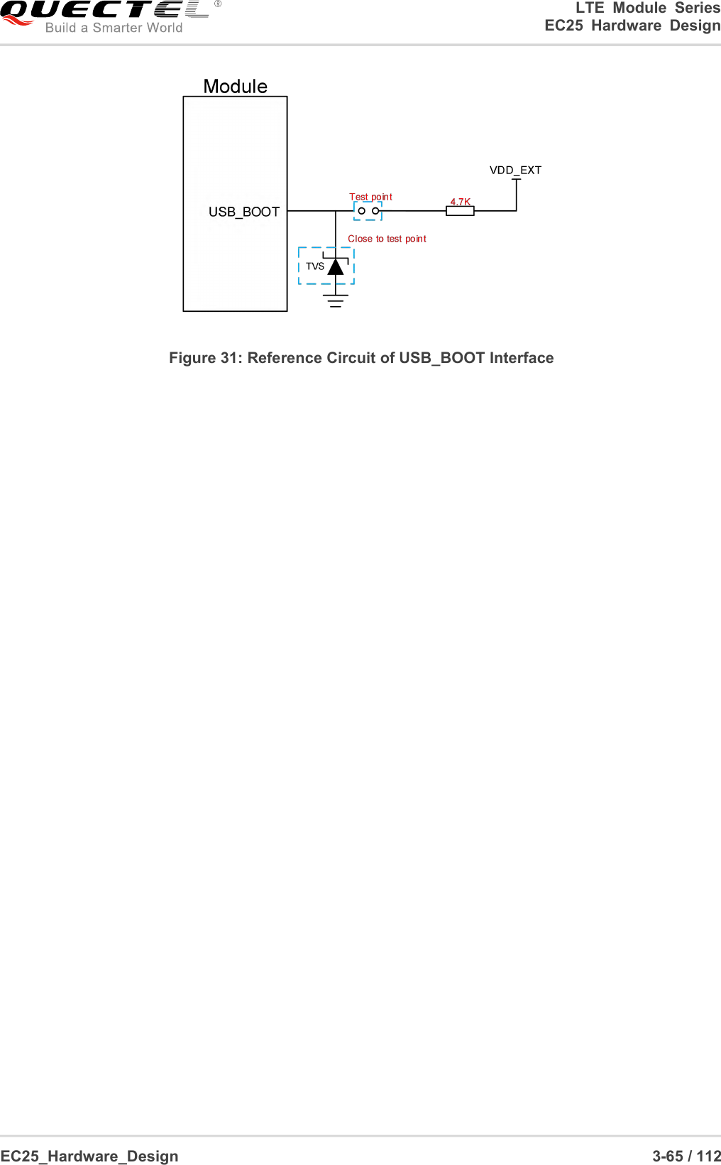
![LTE Module SeriesEC25 Hardware DesignEC25_Hardware_Design 8-103 / 1128.2. Manufacturing and SolderingPush the squeegee to apply the solder paste on the surface of stencil, thus making the paste fill thestencil openings and then penetrate to the PCB. The force on the squeegee should be adjustedproperlyso as to produce a clean stencil surface on a single pass. To ensure the module soldering quality,thethickness of stencil for the module is recommended to be 0.20mm. For more details, please refer todocument [4].It is suggested that the peak reflow temperature is 235ºC~245ºC (for SnAg3.0Cu0.5 alloy). The absolutemaximum reflow temperature is 260ºC. To avoid damage to the module caused by repeated heating, it issuggested that the module should be mounted after reflow soldering for the other side of PCB has beencompleted. Recommended reflow soldering thermal profile is shown below:Figure 48: Reflow Soldering Thermal Profile](https://usermanual.wiki/Quectel-Wireless-Solutions/201607EC25V.Users-Manual/User-Guide-3970452-Page-104.png)
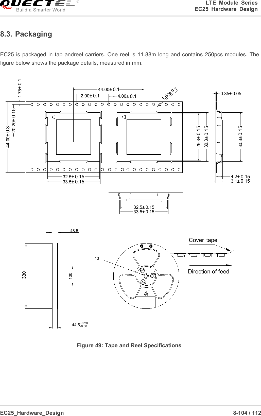
![LTE Module SeriesEC25 Hardware DesignEC25_Hardware_Design 9-105 / 1129Appendix A ReferencesTable 52: Related DocumentsTable 53: Terms and AbbreviationsSNDocument NameRemark[1]Quectel_EC2x&EG9x&EM05_Power_Management_Application_NotePower management application noteforEC25, EC21, EC20 R2.0, EC20 R2.1,EG95, EG91 and EM05 modules[2]Quectel_EC25&EC21_AT_Commands_ManualEC25 and EC21 AT commands manual[3]Quectel_EC25&EC21_GNSS_AT_Commands_ManualEC25 and EC21 GNSS AT commandsmanual[4]Quectel_Module_Secondary_SMT_User_GuideModule secondary SMT user guide[5]Quectel_EC25_Reference_DesignEC25 reference design[6]Quectel_RF_Layout_Application_NoteRF layout application noteAbbreviationDescriptionAMRAdaptive Multi-ratebpsBits Per SecondCHAPChallenge Handshake Authentication ProtocolCSCoding SchemeCSDCircuit Switched DataCTSClear To SendDC-HSPA+Dual-carrier High Speed Packet AccessDFOTADelta Firmware Upgrade Over The AirDLDownlink](https://usermanual.wiki/Quectel-Wireless-Solutions/201607EC25V.Users-Manual/User-Guide-3970452-Page-106.png)