Quectel Wireless Solutions 201609MC20 GSM/GPRS/GNSS Module User Manual
Quectel Wireless Solutions Company Limited GSM/GPRS/GNSS Module
User Manual

MC20 Hardware Design
GSM/GPRS/GNSS Module Series
Rev. MC20_Hardware_Design_V1.0
Date: 2016-07-12
www.quectel.com

GSM/GPRS/GNSS Module Series
MC20 Hardware Design
MC20_Hardware_Design Confidential / Released 1 / 95
Our aim is to provide customers with timely and comprehensive service. For any
assistance, please contact our company headquarters:
Quectel Wireless Solutions Co., Ltd.
Office 501, Building 13, No.99, Tianzhou Road, Shanghai, China, 200233
Tel: +86 21 5108 6236
Email: info@quectel.com
Or our local office. For more information, please visit:
http://www.quectel.com/support/salesupport.aspx
For technical support, or to report documentation errors, please visit:
http://www.quectel.com/support/techsupport.aspx
Or email to: Support@quectel.com
GENERAL NOTES
QUECTEL OFFERS THE INFORMATION AS A SERVICE TO ITS CUSTOMERS. THE INFORMATION
PROVIDED IS BASED UPON CUSTOMERS’ REQUIREMENTS. QUECTEL MAKES EVERY EFFORT
TO ENSURE THE QUALITY OF THE INFORMATION IT MAKES AVAILABLE. QUECTEL DOES NOT
MAKE ANY WARRANTY AS TO THE INFORMATION CONTAINED HEREIN, AND DOES NOT ACCEPT
ANY LIABILITY FOR ANY INJURY, LOSS OR DAMAGE OF ANY KIND INCURRED BY USE OF OR
RELIANCE UPON THE INFORMATION. ALL INFORMATION SUPPLIED HEREIN IS SUBJECT TO
CHANGE WITHOUT PRIOR NOTICE.
COPYRIGHT
THE INFORMATION CONTAINED HERE IS PROPRIETARY TECHNICAL INFORMATION OF QUECTEL
CO., LTD. TRANSMITTING, REPRODUCTION, DISSEMINATION AND EDITING OF THIS DOCUMENT
AS WELL AS UTILIZATION OF THE CONTENT ARE FORBIDDEN WITHOUT PERMISSION.
OFFENDERS WILL BE HELD LIABLE FOR PAYMENT OF DAMAGES. ALL RIGHTS ARE RESERVED
IN THE EVENT OF A PATENT GRANT OR REGISTRATION OF A UTILITY MODEL OR DESIGN.
Copyright © Quectel Wireless Solutions Co., Ltd. 2016. All rights reserved.

GSM/GPRS/GNSS Module Series
MC20 Hardware Design
MC20_Hardware_Design Confidential / Released 2 / 95
About the Document
History
Revision Date Author Description
1.0 2016-07-12 Tiger CHENG Initial

GSM/GPRS/GNSS Module Series
MC20 Hardware Design
MC20_Hardware_Design Confidential / Released 3 / 95
Contents
About the Document ................................................................................................................................ 2
Contents .................................................................................................................................................... 3
Table Index ............................................................................................................................................... 6
Figure Index .............................................................................................................................................. 8
1Introduction ..................................................................................................................................... 10
1.1.Safety Information ................................................................................................................. 10
2Product Concept ............................................................................................................................. 12
2.1.General Description .............................................................................................................. 12
2.2.Directives and Standards ...................................................................................................... 13
2.2.1.2.2.1. FCC Statement .................................................................................................. 13
2.2.2.FCC Radiation Exposure Statement ............................................................................ 13
2.3.Key Features ......................................................................................................................... 13
2.4.Functional Diagram ............................................................................................................... 17
2.5.Evaluation Board ................................................................................................................... 18
3Application Functions..................................................................................................................... 19
3.1.Pin of Module ........................................................................................................................ 20
3.1.1.Pin Assignment ............................................................................................................ 20
3.1.2.Pin Description ............................................................................................................. 21
3.2.Application Modes Introduction ............................................................................................. 25
3.3.Power Supply ........................................................................................................................ 27
3.3.1.Power Features ........................................................................................................... 27
3.3.2.Decrease Supply Voltage Drop .................................................................................... 28
3.3.2.1.Decrease Supply Voltage Drop for GSM Part .................................................. 28
3.3.2.2.Decrease Supply Voltage Drop for GNSS Part ................................................ 29
3.3.3.Reference Design for Power Supply ............................................................................ 30
3.3.3.1.Reference Design for Power Supply of GSM Part ........................................... 30
3.3.3.2.Reference Design for Power Supply of GNSS Part ......................................... 31
3.3.4.Monitor Power Supply .................................................................................................. 31
3.3.5.Backup Domain of GNSS ............................................................................................ 31
3.4.Operating Modes .................................................................................................................. 32
3.4.1.Operating Modes of GSM Part ..................................................................................... 32
3.4.1.1.Minimum Functionality Mode ........................................................................... 33
3.4.1.2.SLEEP Mode ................................................................................................... 34
3.4.1.3.Wake up GSM Part from SLEEP Mode ........................................................... 34
3.4.2.Operating Modes of GNSS Part ................................................................................... 34
3.4.2.1.Full on Mode.................................................................................................... 34
3.4.2.2.Standby Mode ................................................................................................. 36
3.4.2.3.Backup Mode .................................................................................................. 36

GSM/GPRS/GNSS Module Series
MC20 Hardware Design
MC20_Hardware_Design Confidential / Released 4 / 95
3.4.3.Summary of GSM and GNSS Parts’ State in All-in-one Solution .................................. 37
3.4.4.Summary of GSM and GNSS Parts’ State in Stand-alone Solution ............................. 37
3.5.Power on and down .............................................................................................................. 38
3.5.1.Power on ..................................................................................................................... 38
3.5.2.Power down ................................................................................................................. 40
3.5.2.1.Power down Module Using the PWRKEY Pin ................................................. 40
3.5.2.2.Power down Module Using AT Command ....................................................... 41
3.5.2.3.Power down GNSS Part Alone Using AT Command ....................................... 42
3.5.2.4.Under-voltage Automatic Shutdown ................................................................ 42
3.6.Serial Interfaces .................................................................................................................... 43
3.6.1.UART Port ................................................................................................................... 45
3.6.1.1.Features of UART Port .................................................................................... 45
3.6.1.2.The Connection of UART ................................................................................ 46
3.6.1.3.Firmware Upgrade ........................................................................................... 48
3.6.2.Debug Port................................................................................................................... 49
3.6.3.Auxiliary UART Port and GNSS UART Port ................................................................. 49
3.6.3.1.Connection in All-in-one Solution ..................................................................... 49
3.6.3.2.Connection in Stand-alone Solution ................................................................ 50
3.6.4.UART Application ......................................................................................................... 51
3.7.Audio Interfaces .................................................................................................................... 52
3.7.1.Decrease TDD Noise and Other Noises ...................................................................... 54
3.7.2.Microphone Interfaces Design ..................................................................................... 54
3.7.3.Receiver and Speaker Interface Design ...................................................................... 55
3.7.4.Earphone Interface Design .......................................................................................... 56
3.7.5.Loud Speaker Interface Design.................................................................................... 56
3.7.6.Audio Characteristics ................................................................................................... 57
3.8.SIM Card Interface ................................................................................................................ 57
3.9.ADC ...................................................................................................................................... 61
3.10.Behaviors of the RI ............................................................................................................... 61
3.11.Network Status Indication ...................................................................................................... 63
3.12.EASY Autonomous AGPS Technology ................................................................................. 64
3.13.EPO Offline AGPS Technology ............................................................................................. 64
3.14.Multi-tone AIC ....................................................................................................................... 65
4Antenna Interface ............................................................................................................................ 66
4.1.GSM Antenna Interface ......................................................................................................... 66
4.1.1.Reference Design ........................................................................................................ 66
4.1.2.RF Output Power ......................................................................................................... 67
4.1.3.RF Receiving Sensitivity .............................................................................................. 68
4.1.4.Operating Frequencies ................................................................................................ 68
4.1.5.RF Cable Soldering ..................................................................................................... 68
4.2.GNSS Antenna Interface ....................................................................................................... 69
4.2.1.Antenna Specifications ................................................................................................ 69
4.2.2.Active Antenna ............................................................................................................. 70
4.2.3.Passive Antenna .......................................................................................................... 71

GSM/GPRS/GNSS Module Series
MC20 Hardware Design
MC20_Hardware_Design Confidential / Released 5 / 95
4.3.Bluetooth Antenna Interface .................................................................................................. 71
5Electrical, Reliability and Radio Characteristics .......................................................................... 74
5.1.Absolute Maximum Ratings .................................................................................................. 74
5.2.Operating Temperature ......................................................................................................... 74
5.3.Power Supply Ratings ........................................................................................................... 75
5.4.Current Consumption ............................................................................................................ 77
5.5.Electrostatic Discharge ......................................................................................................... 79
6Mechanical Dimensions.................................................................................................................. 81
6.1.Mechanical Dimensions of Module ....................................................................................... 81
6.2.Recommended Footprint ....................................................................................................... 83
6.3.Top and Bottom View of the Module ...................................................................................... 84
7Storage and Manufacturing ............................................................................................................ 85
7.1.Storage.................................................................................................................................. 85
7.2.Soldering ............................................................................................................................... 85
7.3.Packaging ............................................................................................................................. 86
7.3.1.Tape and Reel Packaging ............................................................................................ 87
8Appendix A References .................................................................................................................. 88
9Appendix B GPRS Coding Schemes ............................................................................................. 93
10Appendix C GPRS Multi-slot Classes ............................................................................................ 95

GSM/GPRS/GNSS Module Series
MC20 Hardware Design
MC20_Hardware_Design Confidential / Released 6 / 95
Table Index
TABLE 1: KEY FEATURES (GMS/GPRS PART OF MC20) .................................................................... 13
TABLE 2: CODING SCHEMES AND MAXIMUM NET DATA RATES OVER AIR INTERFACE ............... 15
TABLE 3: KEY FEATURES (GNSS PART OF MC20) ............................................................................. 16
TABLE 4: PROTOCOLS SUPPORTED BY THE MODULE ..................................................................... 17
TABLE 5: I/O PARAMETERS DEFINITION ............................................................................................. 21
TABLE 6: PIN DESCRIPTION ................................................................................................................. 21
TABLE 7: MULTIPLEXED FUNCTIONS .................................................................................................. 25
TABLE 8: COMPARISON BETWEEN ALL-IN-ONE AND STAND-ALONE SOLUTION ........................... 27
TABLE 9: OPERATING MODES OVERVIEW OF GSM PART ................................................................ 32
TABLE 10: DEFAULT CONFIGURATION OF FULL ON MODE (GNSS PART) ...................................... 35
TABLE 11: COMBINATION STATES OF GSM AND GNSS PARTS IN ALL-IN-ONE SOLUTION ........... 37
TABLE 12: COMBINATION STATES OF GSM AND GNSS PARTS IN STAND-ALONE SOLUTION ...... 37
TABLE 13: LOGIC LEVELS OF THE UART INTERFACE ....................................................................... 44
TABLE 14: PIN DEFINITION OF THE UART INTERFACES ................................................................... 44
TABLE 15: PIN DEFINITION OF AUDIO INTERFACE ............................................................................ 52
TABLE 16: AOUT2 OUTPUT CHARACTERISTICS ................................................................................ 53
TABLE 17: TYPICAL ELECTRET MICROPHONE CHARACTERISTICS ................................................ 57
TABLE 18: TYPICAL SPEAKER CHARACTERISTICS ........................................................................... 57
TABLE 19: PIN DEFINITION OF THE SIM INTERFACE ......................................................................... 58
TABLE 20: PIN DEFINITION OF THE ADC ............................................................................................. 61
TABLE 21: CHARACTERISTICS OF THE ADC ...................................................................................... 61
TABLE 22: BEHAVIORS OF THE RI ....................................................................................................... 61
TABLE 23: WORKING STATE OF THE NETLIGHT ................................................................................ 63
TABLE 24: PIN DEFINITION OF THE RF_ANT ...................................................................................... 66
TABLE 25: ANTENNA CABLE REQUIREMENTS ................................................................................... 67
TABLE 26: ANTENNA REQUIREMENTS ................................................................................................ 67
TABLE 27: RF OUTPUT POWER ........................................................................................................... 67
TABLE 28: RF RECEIVING SENSITIVITY .............................................................................................. 68
TABLE 29: OPERATING FREQUENCIES ............................................................................................... 68
TABLE 30: RECOMMENDED ANTENNA SPECIFICATIONS ................................................................. 69
TABLE 31: PIN DEFINITION OF THE BT_ANT ...................................................................................... 72
TABLE 32: ABSOLUTE MAXIMUM RATINGS ........................................................................................ 74
TABLE 33: OPERATING TEMPERATURE .............................................................................................. 75
TABLE 34: POWER SUPPLY RATINGS OF GSM PART (GNSS IS POWERED OFF) ........................... 75
TABLE 35: POWER SUPPLY RATINGS OF GNSS PART ...................................................................... 76
TABLE 36: CURRENT CONSUMPTION OF GSM PART (GNSS IS POWERED OFF) .......................... 77
TABLE 37: CURRENT CONSUMPTION OF THE GNSS PART .............................................................. 79
TABLE 38: ESD ENDURANCE (TEMPERATURE: 25ºC, HUMIDITY: 45%) ........................................... 79
TABLE 39: REEL PACKAGING ............................................................................................................... 87
TABLE 40: RELATED DOCUMENTS ...................................................................................................... 88
TABLE 41: TERMS AND ABBREVIATIONS ............................................................................................ 89

GSM/GPRS/GNSS Module Series
MC20 Hardware Design
MC20_Hardware_Design Confidential / Released 7 / 95
TABLE 42: DESCRIPTION OF DIFFERENT CODING SCHEMES ......................................................... 93
TABLE 43: GPRS MULTI-SLOT CLASSES ............................................................................................. 95

GSM/GPRS/GNSS Module Series
MC20 Hardware Design
MC20_Hardware_Design Confidential / Released 8 / 95
Figure Index
FIGURE 1: MODULE FUNCTIONAL DIAGRAM ..................................................................................... 18
FIGURE 2: PIN ASSIGNMENT ............................................................................................................... 20
FIGURE 3: ALL-IN-ONE SOLUTION SCHEMATIC DIAGRAM ............................................................... 26
FIGURE 4: STAND-ALONE SOLUTION SCHEMATIC DIAGRAM .......................................................... 26
FIGURE 5: VOLTAGE RIPPLE DURING TRANSMITTING (GSM PART) ............................................... 28
FIGURE 6: REFERENCE CIRCUIT FOR THE VBAT INPUT (GSM PART) ............................................ 29
FIGURE 7: REFERENCE CIRCUIT FOR THE GNSS_VCC INPUT ....................................................... 29
FIGURE 8: REFERENCE CIRCUIT FOR POWER SUPPLY OF THE GSM PART ................................. 30
FIGURE 9: REFERENCE CIRCUIT DESIGN FOR GNSS PART ............................................................ 31
FIGURE 10: INTERNAL GNSS’S BACKUP DOMAIN POWER CONSTRUCTION ................................. 32
FIGURE 11: TURN ON THE MODULE WITH AN OPEN-COLLECTOR DRIVER ................................... 38
FIGURE 12: TURN ON THE MODULE WITH A BUTTON ...................................................................... 39
FIGURE 13: TURN-ON TIMING .............................................................................................................. 39
FIGURE 14: TURN-OFF TIMING BY USING THE PWRKEY PIN ........................................................... 41
FIGURE 15: TURN-OFF TIMING OF GNSS PART BY USING AT COMMAND ...................................... 42
FIGURE 16: REFERENCE DESIGN FOR FULL-FUNCTION UART ...................................................... 47
FIGURE 17: REFERENCE DESIGN FOR UART PORT (THREE LINE CONNECTION) ........................ 47
FIGURE 18: REFERENCE DESIGN FOR UART PORT WITH HARDWARE FLOW CONTROL............ 48
FIGURE 19: REFERENCE DESIGN FOR FIRMWARE UPGRADE ....................................................... 48
FIGURE 20: REFERENCE DESIGN FOR DEBUG PORT ...................................................................... 49
FIGURE 21: AUXILIARY AND GNSS UART PORT CONNECTION IN ALL-IN-ONE SOLUTION ........... 50
FIGURE 22: AUXILIARY AND GNSS UART PORT CONNECTION IN STAND-ALONE SOLUTION ...... 51
FIGURE 23: LEVEL MATCH DESIGN FOR 3.3V SYSTEM .................................................................... 51
FIGURE 24: SKETCH MAP FOR RS-232 INTERFACE MATCH ............................................................ 52
FIGURE 25: REFERENCE DESIGN FOR AIN ........................................................................................ 54
FIGURE 26: HANDSET INTERFACE DESIGN FOR AOUT1 .................................................................. 55
FIGURE 27: SPEAKER INTERFACE DESIGN WITH AN AMPLIFIER FOR AOUT1 .............................. 55
FIGURE 28: EARPHONE INTERFACE DESIGN .................................................................................... 56
FIGURE 29: LOUD SPEAKER INTERFACE DESIGN ............................................................................ 56
FIGURE 30: REFERENCE CIRCUIT FOR SIM1 INTERFACE WITH AN 8-PIN SIM CARD HOLDER ... 59
FIGURE 31: REFERENCE CIRCUIT FOR SIM1 INTERFACE WITH A 6-PIN SIM CARD HOLDER ...... 59
FIGURE 32: REFERENCE CIRCUIT FOR SIM2 INTERFACE WITH A 6-PIN SIM CARD HOLDER ...... 60
FIGURE 33: RI BEHAVIOR AS A RECEIVER WHEN VOICE CALLING ................................................. 62
FIGURE 34: RI BEHAVIOR AS A CALLER.............................................................................................. 62
FIGURE 35: RI BEHAVIOR WHEN URC OR SMS RECEIVED .............................................................. 62
FIGURE 36: REFERENCE DESIGN FOR NETLIGHT ............................................................................ 63
FIGURE 37: REFERENCE DESIGN FOR GSM ANTENNA ................................................................... 66
FIGURE 38: RF SOLDERING SAMPLE ................................................................................................. 69
FIGURE 39: REFERENCE DESIGN WITH ACTIVE ANTENNA ............................................................. 70
FIGURE 40: REFERENCE DESIGN WITH PASSIVE ANTENNA ........................................................... 71
FIGURE 41: REFERENCE DESIGN FOR BLUETOOTH ANTENNA ...................................................... 72

GSM/GPRS/GNSS Module Series
MC20 Hardware Design
MC20_Hardware_Design Confidential / Released 9 / 95
FIGURE 42: MC20 TOP AND SIDE DIMENSIONS (UNIT: MM) .............................................................. 81
FIGURE 43: MC20 BOTTOM DIMENSIONS (UNIT: MM) ....................................................................... 82
FIGURE 44: RECOMMENDED FOOTPRINT (UNIT: MM) ...................................................................... 83
FIGURE 45: TOP VIEW OF THE MODULE ............................................................................................ 84
FIGURE 46: BOTTOM VIEW OF THE MODULE .................................................................................... 84
FIGURE 47: REFLOW SOLDERING THERMAL PROFILE .................................................................... 86
FIGURE 48: TAPE AND REEL SPECIFICATION .................................................................................... 87
FIGURE 49: DIMENSIONS OF REEL ..................................................................................................... 87
FIGURE 50: RADIO BLOCK STRUCTURE OF CS-1, CS-2 AND CS-3 .................................................. 93
FIGURE 51: RADIO BLOCK STRUCTURE OF CS-4 ............................................................................. 94

GSM/GPRS/GNSS Module Series
MC20 Hardware Design
MC20_Hardware_Design Confidential / Released 10 / 95
1 Introduction
This document defines the MC20 module and describes its hardware interface which is connected with
the customer application as well as its air interface.
The document can help you quickly understand module interface specifications, as well as the electrical
and mechanical details. Associated with application note and user guide, you can use MC20 module to
design and set up mobile applications easily.
1.1. Safety Information
The following safety precautions must be observed during all phases of the operation, such as usage,
service or repair of any cellular terminal or mobile incorporating MC20 module. Manufacturers of the
cellular terminal should send the following safety information to users and operating personnel, and
incorporate these guidelines into all manuals supplied with the product. If not so, Quectel assumes no
liability for the customer’s failure to comply with these precautions.
Full attention must be given to driving at all times in order to reduce the risk of an
accident. Using a mobile while driving (even with a handsfree kit) causes
distraction and can lead to an accident. You must comply with laws and regulations
restricting the use of wireless devices while driving.
Switch off the cellular terminal or mobile before boarding an aircraft. Make sure it is
switched off. The operation of wireless appliances in an aircraft is forbidden, so as
to prevent interference with communication systems. Consult the airline staff about
the use of wireless devices on boarding the aircraft, if your device offers a Airplane
Mode which must be enabled prior to boarding an aircraft.
Switch off your wireless device when in hospitals, clinics or other health care
facilities. These requests are desinged to prevent possible interference with
sentitive medical equipment.

GSM/GPRS/GNSS Module Series
MC20 Hardware Design
MC20_Hardware_Design Confidential / Released 11 / 95
Cellular terminals or mobiles operating over radio frequency signal and cellular
network cannot be guaranteed to connect in all conditions, for example no mobile
fee or with an invalid SIM card. While you are in this condition and need emergent
help, please remember using emergency call. In order to make or receive a call,
the cellular terminal or mobile must be switched on and in a service area with
adequate cellular signal strength.
Your cellular terminal or mobile contains a transmitter and receiver. When it is ON ,
it receives and transmits radio frequency energy. RF interference can occur if it is
used close to TV set, radio, computer or other electric equipment.
In locations with potencially explosive atmospheres, obey all posted signs to turn
off wireless devices such as your phone or other cellular terminals. Areas with
potencially explosive atmospheres include fuelling areas, below decks on boats,
fuel or chemical transfer or storage facilities, areas where the air contains
chemicals or particles such as grain, dust or metal powders, etc.

GSM/GPRS/GNSS Module Series
MC20 Hardware Design
MC20_Hardware_Design Confidential / Released 12 / 95
2 Product Concept
2.1. General Description
MC20 is a multi-purpose module which integrates a high performance GNSS engine and a quad-band
GSM/GPRS engine. It can work as all-in-one solution or stand-alone solution according to customers'
application demands. For detailed introduction on all-in-one solution and stand-alone solution, please
refer to Chapter 3.2.
The quad-band GSM/GPRS engine can work at frequencies of GSM850MHz, EGSM900MHz,
DCS1800MHz and PCS1900MHz. MC20 features GPRS multi-slot class 12 and supports the GPRS
coding schemes CS-1, CS-2, CS-3 and CS-4. For more details about GPRS multi-slot classes and coding
schemes, please refer to the Appendix B & C.
The GNSS engine is a single receiver integrating GPS and BeiDou systems. It supports multiple
positioning and navigation systems including autonomous GPS, BeiDou, SBAS (including WAAS,
EGNOS, MSAS and GAGAN), and QZSS. It is able to achieve the industry’s highest level of sensitivity,
accuracy and TTFF with the lowest power consumption. The embedded flash memory provides capacity
for storing user-specific configurations and allows for future updates.
MC20 is an SMD type module with 54 LCC pads and 14 LGA pads which can be easily embedded into
applications. With a compact profile of 18.7mm × 16.0mm × 2.1mm, the module can meet almost all the
requirements for M2M applications, including vehicle and personal tracking, wearable devices, security
systems, wireless POS, industrial PDA, smart metering, remote maintenance & control, etc.
Designed with power saving technique, the current consumption of MC20’s GSM part is as low as 1.2mA
in SLEEP mode when DRX is 5 and the GNSS part is powered off. The GNSS engine also has many
advanced power saving modes including standby and backup modes which can fit the requirement of
low-power consumption in different scenes.
GSM part of MC20 is integrated with Internet service protocols such as TCP, UDP, PPP, HTTP and FTP.
Extended AT commands have been developed for you to use these Internet service protocols easily.
EASY technology as a key feature of GNSS part of MC20 module is one kind of AGPS. Capable of
collecting and processing all internal aiding information like GNSS time, ephemeris, last position, etc., the
GNSS part will have a fast TTFF in either Hot or Warm start.

GSM/GPRS/GNSS Module Series
MC20 Hardware Design
MC20_Hardware_Design Confidential / Released 13 / 95
The module fully complies with the RoHS directive of the European Union.
2.2. Directives and Standards
The MC20module is designed to comply with the FCC statements. FCC ID: XMR201609MC20
The Host system using MC20 should have label “contains FCC ID: XMR201609MC20”.
2.2.1. 2.2.1. FCC Statement
Changes or modifications not expressly approved by the party responsible for compliance could void the
user’s authority to operate the equipment.
2.2.2. FCC Radiation Exposure Statement
This equipment complies with FCC radiation exposure limits set forth for an uncontrolled environment.
This equipment should be installed and operated with minimum distance 20cm between the radiator and
your body as well as kept minimum 20cm from radio antenna depending on the Mobile status of this
module usage. This module should NOT be installed and operating simultaneously with other radio. The
manual of the host system, which uses MC20, must include RF exposure warning statement to advice
user should keep minimum 20cm from the radio antenna of MC20 module depending on the Mobile status.
Note: If a portable device (such as PDA) uses MC20 module, the device needs to do permissive change
and SAR testing.
The following list indicates the performance of antenna gain in certificate testing.
Part
Number Frequency Range (MHz) Peak Gain
(XZ-V)
Average
Gain(XZ-V) VSWR Impedance
3R007 GSM850:824~894MHz
PCS1900: 1850~1990MHz 1 dBi typ. 1 dBi typ. 2 max 50Ω
2.3. Key Features
The following table describes the detailed features of MC20 module.
Table 1: Key Features (GMS/GPRS Part of MC20)
Features Implementation

GSM/GPRS/GNSS Module Series
MC20 Hardware Design
MC20_Hardware_Design Confidential / Released 14 / 95
Power Supply Single supply voltage: 3.3V ~ 4.6V
Typical supply voltage: 4V
Power Saving
Typical power consumption in SLEEP mode (GNSS is powered off):
1.2mA@DRX=5
0.8mA@DRX=9
Frequency Bands
Quad-band: GSM850, EGSM900, DCS1800, PCS1900.
The module can search these frequency bands automatically
The frequency bands can be set by AT commands
Compliant to GSM Phase 2/2+
GSM Class Small MS
Transmitting Power Class 4 (2W) at GSM850 and EGSM900
Class 1 (1W) at DCS1800 and PCS1900
GPRS Connectivity
GPRS multi-slot class 12 (default)
GPRS multi-slot class 1~12 (configurable)
GPRS mobile station class B
DATA GPRS
GPRS data downlink transfer: max. 85.6kbps
GPRS data uplink transfer: max. 85.6kbps
Coding scheme: CS-1, CS-2, CS-3 and CS-4
Support the protocols PAP (Password Authentication Protocol)
usually used for PPP connections
Internet service protocols TCP/UDP, FTP, PPP, HTTP, NTP, PING
Support Packet Broadcast Control Channel (PBCCH)
Support Unstructured Supplementary Service Data (USSD)
Temperature Range Operation temperature range: -35°C ~ +75°C 1)
Extended temperature range: -40°C ~ +85°C 2)
SMS Text and PDU mode
SMS storage: SIM card
SIM Interface Support SIM card: 1.8V, 3.0V
Support Dual SIM Single Standby
Audio Features
Speech codec modes:
Half Rate (ETS 06.20)
Full Rate (ETS 06.10)
Enhanced Full Rate (ETS 06.50/06.60/06.80)
Adaptive Multi-Rate (AMR)
Echo Suppression
Noise Reduction
Embedded one amplifier of class AB with maximum driving power up
to 800mW
UART Interfaces
UART Port:
Seven lines on UART port interface
Used for AT command and GPRS data
Used for PMTK command and NMEA output in all-in-one solution
GSM/GPRS/GNSS Module Series
MC20 Hardware Design
MC20_Hardware_Design Confidential / Released 15 / 95
1. 1) Within operation temperature range, the module is 3GPP compliant.
2. 2) Within extended temperature range, the module remains the ability to establish and maintain a
voice, SMS, data transmission, emergency call, etc. There is no unrecoverable malfunction. There
are also no effects on radio spectrum and no harm to radio network. Only one or more parameters like
Pout might reduce in their value and exceed the specified tolerances. When the temperature returns to
the normal operating temperature levels, the module will meet 3GPP compliant again.
Table 2: Coding Schemes and Maximum Net Data Rates over Air Interface
Multiplexing function
Support autobauding from 4800bps to 115200bps
Debug Port:
Two lines on debug port interface DBG_TXD and DBG_RXD
Debug port only used for firmware debugging
Auxiliary Port:
Two lines on auxiliary port interface: TXD_AUX and RXD_AUX
Used for communication with the GNSS Part in all-in-one solution
Phonebook Management Support phonebook types: SM, ME, ON, MC, RC, DC, LD, LA
SIM Application Toolkit Support SAT class 3, GSM 11.14 Release 99
Physical Characteristics Size: (18.7±0.15) × (16±0.15) × (2.1±0.2)mm
Weight: Approx. 1.3g
Firmware Upgrade Firmware upgrade via UART port
Antenna Interface Connected to antenna pad with 50 Ohm impedance control
Coding Scheme 1 Timeslot 2 Timeslot 4 Timeslot
CS-1 9.05kbps 18.1kbps 36.2kbps
CS-2 13.4kbps 26.8kbps 53.6kbps
CS-3 15.6kbps 31.2kbps 62.4kbps
CS-4 21.4kbps 42.8kbps 85.6kbps
NOTES

GSM/GPRS/GNSS Module Series
MC20 Hardware Design
MC20_Hardware_Design Confidential / Released 16 / 95
Table 3: Key Features (GNSS Part of MC20)
Features Implementation
GNSS GPS+BeiDou
Power Supply Supply voltage: 2.8V~4.3V Typical: 3.3V
Power Consumption
Acquisition: 25mA @-130dBm (GPS)
Tracking: 19mA @-130dBm (GPS)
Acquisition: 23mA @-130dBm (GPS+BeiDou)
Tracking: 18mA @-130dBm (GPS+BeiDou)
Standby: 300uA @VCC=3.3V
Backup: 14uA @V_BCKP=3.3V
Receiver Type GPS L1 1575.42MHz C/A Code
BeiDou B1 1561.098MHz C/A Code
Sensitivity
GPS+BeiDou
Acquisition: -148dBm
Reacquisition: -160dBm
Tracking: -163dBm
Time-to-First-Fix
(EASY Enabled) 1)
Cold Start: <15s average @-130dBm
Warm Start: <5s average @-130dBm
Hot Start: 1s @-130dBm
Time-to-First-Fix
(EASY Disabled)
Cold Start (Autonomous): <35s average @-130dBm
Warm Start (Autonomous): <30s average @-130dBm
Hot Start (Autonomous): 1s @-130dBm
Horizontal Position
Accuracy (Autonomous) <2.5 m CEP @-130dBm
Update Rate Up to 10Hz, 1Hz by default
Velocity Accuracy Without aid: 0.1m/s
Acceleration Accuracy Without aid: 0.1m/s²
Dynamic Performance
Maximum Altitude: 18,000m
Maximum Velocity: 515m/s
Acceleration: 4G
GNSS UART Port
GNSS UART port: GNSS_TXD and GNSS_ RXD
Support baud rate from 4800bps to 115200bps; 115200bps by
default
Used for communication with the GSM Part in all-in-one solution
Used for communication with peripherals in stand-alone solution
NOTE
GSM/GPRS/GNSS Module Series
MC20 Hardware Design
MC20_Hardware_Design Confidential / Released 17 / 95
1) In this mode, GNSS part’s backup domain should be valid.
Table 4: Protocols Supported by the Module
Please refer to document [2] for details of NMEA standard protocol and MTK proprietary protocol.
2.4. Functional Diagram
The following figure shows a block diagram of MC20 and illustrates the major functional parts.
Radio frequency part
Power management
Peripheral interfaces
—Power supply
—Turn-on/off interface
—UART interface
—Audio interface
—SIM interface
—ADC interface
—RF interface
—PCM interface
—BT interface
—SD interface
Protocol Type
NMEA output, ASCII, 0183, 3.01
PMTK Input/output, MTK proprietary protocol
NOTE
GSM/GPRS/GNSS Module Series
MC20 Hardware Design
MC20_Hardware_Design Confidential / Released 18 / 95
Figure 1: Module Functional Diagram
2.5. Evaluation Board
In order to help you develop applications with MC20, Quectel supplies an evaluation board (EVB), TE-A
board, RS-232 to USB cable, power adapter, earphone, GSM antenna, GNSS antenna and other
peripherals to control or test the module. For details, please refer to document [11].

GSM/GPRS/GNSS Module Series
MC20 Hardware Design
MC20_Hardware_Design Confidential / Released 19 / 95
3 Application Functions
MC20 is an SMD type module with 54 LCC pads and 14 LGA pads. The following chapters provide
detailed descriptions about these pins.
Pin of module
Power supply
Operating modes
Power on/down
Power saving
Backup domain of GNSS
Serial interfaces
Audio interfaces
SIM card interface
ADC
Behaviors of the RI
Network status indication
RF transmitting signal indication
EASY autonomous AGPS technology
EPO offline AGPS technology
Multi-tone AIC
GSM/GPRS/GNSS Module Series
MC20 Hardware Design
MC20_Hardware_Design Confidential / Released 20 / 95
3.1. Pin of Module
3.1.1. Pin Assignment
Figure 2: Pin Assignment
Please keep all reserved pins open.
NOTE

GSM/GPRS/GNSS Module Series
MC20 Hardware Design
MC20_Hardware_Design Confidential / Released 21 / 95
3.1.2. Pin Description
Table 5: I/O Parameters Definition
Type Description
IO Bidirectional input/output
DI Digital input
DO Digital output
PI Power input
PO Power output
AI Analog input
AO Analog output
Table 6: Pin Description
Power Supply
PIN Name PIN No. I/O Description DC Characteristics Comment
VBAT 50, 51 PI
Power supply of
GSM/GPRS part:
VBAT=3.3V~4.6V
VImax=4.6V
VImin=3.3V
VInorm=4.0V
It must be able to
provide sufficient
current up to 1.6A
in a transmitting
burst.
GNSS_
VCC 26 PI
Power supply of GNSS
part:
GNSS_VCC=2.8V~4.3V
VImax=4.3V
VImin=2.8V
VInorm=3.3V
Assure load
current no less
than 150mA.
VRTC 52 IO Keep this pin
open
VDD_
EXT 43 PO
Supply 2.8V voltage for
external circuit.
VOmax=2.9V
VOmin=2.7V
VOnorm=2.8V
IOmax=20mA
1. If unused, keep
this pin open.
2. Recommend
adding a
2.2~4.7uF bypass
capacitor, when
using this pin for
power supply.
GND 14,27, Ground

GSM/GPRS/GNSS Module Series
MC20 Hardware Design
MC20_Hardware_Design Confidential / Released 22 / 95
31,40,
42,44,
45,48,
49
Turn on/off
PIN Name PIN No. I/O Description DC Characteristics Comment
PWRKEY 5 DI
Power on/off key.
PWRKEY should be
pulled down for a
moment to turn on or
turn off the system.
VILmax=
0.1×VBAT
VIHmin=
0.6×VBAT
VIHmax=3.1V
Audio Interface
PIN Name PIN No. I/O Description DC Characteristics Comment
MICP
MICN
1,
2 AI Positive and negative
voice input
Refer to Chapter 3.7.6
If unused, keep
these pins open.
SPKP
SPKN
3,
4 AO Channel 1 positive and
negative voice output
If unused, keep
these pins open.
Support both
voice and
ringtone output.
LOUD
SPKP
LOUD
SPKN
54
53 AO Channel 2 positive and
negative voice output
1. If unused, keep
these pins open.
2. Integrate a
Class- AB
amplifier
internally.
3. Support both
voice and
ringtone output.
Network Status Indicator
PIN Name PIN No. I/O Description DC Characteristics Comment
NETLIGHT 47 DO Network status
indication
VOHmin=
0.85×VDD_EXT
VOLmax=
0.15×VDD_EXT
If unused, keep
this pin open.
UART Port
PIN Name PIN No. I/O Description DC Characteristics Comment
TXD 34 DO Transmit data VILmin=0V If only TXD, RXD

GSM/GPRS/GNSS Module Series
MC20 Hardware Design
MC20_Hardware_Design Confidential / Released 23 / 95
RXD 33 DI Receive data VILmax=
0.25×VDD_EXT
VIHmin=
0.75×VDD_EXT
VIHmax=
VDD_EXT+0.2
VOHmin=
0.85×VDD_EXT
VOLmax=
0.15×VDD_EXT
and GND are
used for
communication, it
is recommended
to keep all other
pins open.
DTR 37 DI Data terminal ready
RI 35 DO Ring indication
DCD 36 DO Data carrier detection
CTS 38 DO Clear to send
RTS 39 DI Request to send
Debug Port
PIN Name PIN No. I/O Description DC Characteristics Comment
DBG_
TXD 29 DO Transmit data The same as UART
port
If unused, keep
these pins open.
DBG_
RXD 30 DI Receive data
Auxiliary UART Port
PIN Name PIN No. I/O Description DC Characteristics Comment
TXD_
AUX 25 DO Transmit data The same as UART
port
Refer to Chapter
3.6.3
RXD_
AUX 24 DI Receive data
GNSS UART Port
PIN Name PIN No. I/O Description DC Characteristics Comment
GNSS_
TXD 22 DO Transmit data VOLmax=0.42V
VOHmin=2.4V
VOHnom=2.8V
VILmin=-0.3V
VILmax=0.7V
VIHmin=2.1V
VIHmax=3.1V
Refer to Chapter
3.6.3
GNSS_
RXD 23 DI Receive data
SIM Interface
PIN Name PIN No. I/O Description DC Characteristics Comment
SIM1_ VDD
SIM2_ VDD
18
13 PO Power supply for SIM
card
The voltage can be
selected by software
automatically. Either
1.8V or 3.0V.
All signals of SIM
interface should
be protected
against ESD with
a TVS diode
array.
SIM1_ CLK
SIM2_ CLK
19
10 DO SIM clock VOLmax=
0.15×SIM_VDD

GSM/GPRS/GNSS Module Series
MC20 Hardware Design
MC20_Hardware_Design Confidential / Released 24 / 95
VOHmin=
0.85×SIM_VDD
Maximum trace
length is 200mm
from the module
pad to SIM card
holder.
SIM1_
DATA
SIM2_
DATA
21
11 IO SIM data
VILmax=
0.25×SIM_VDD
VIHmin=
0.75×SIM_VDD
VOLmax=
0.15×SIM_VDD
VOHmin=
0.85×SIM_VDD
SIM1_ RST
SIM2_ RST
20
12 DO SIM reset
VOLmax=
0.15×SIM_VDD
VOHmin=
0.85×SIM_VDD
SIM_
GND 16 SIM ground
SIM1_
PRESENCE 37 I SIM1 card detection
VILmin =0V
VILmax =
0.25×VDD_EXT
VIHmin =
0.75×VDD_EXT
VIHmax =
VDD_EXT+0.2
ADC
PIN Name PIN No. I/O Description DC Characteristics Comment
ADC 6 AI
General purpose
analog to digital
converter.
Voltage range:
0V to 2.8V
If unused, keep
this pin open.
Digital Audio Interface (PCM)
PCM_CLK 59 DO PCM clock
If unused, keep
these pins open
PCM_OUT 60 DO PCM data output
PCM_SYNC 61 DO PCM frame
synchronization
PCM_IN 62 DI PCM data input
SD Card Interface
SD_CMD 7 DO SD Command line
If unused, keep
these pins open
SD_CLK 8 DO SD clock
SD_DATA 9 IO SD data line

GSM/GPRS/GNSS Module Series
MC20 Hardware Design
MC20_Hardware_Design Confidential / Released 25 / 95
Table 7: Multiplexed Functions
3.2. Application Modes Introduction
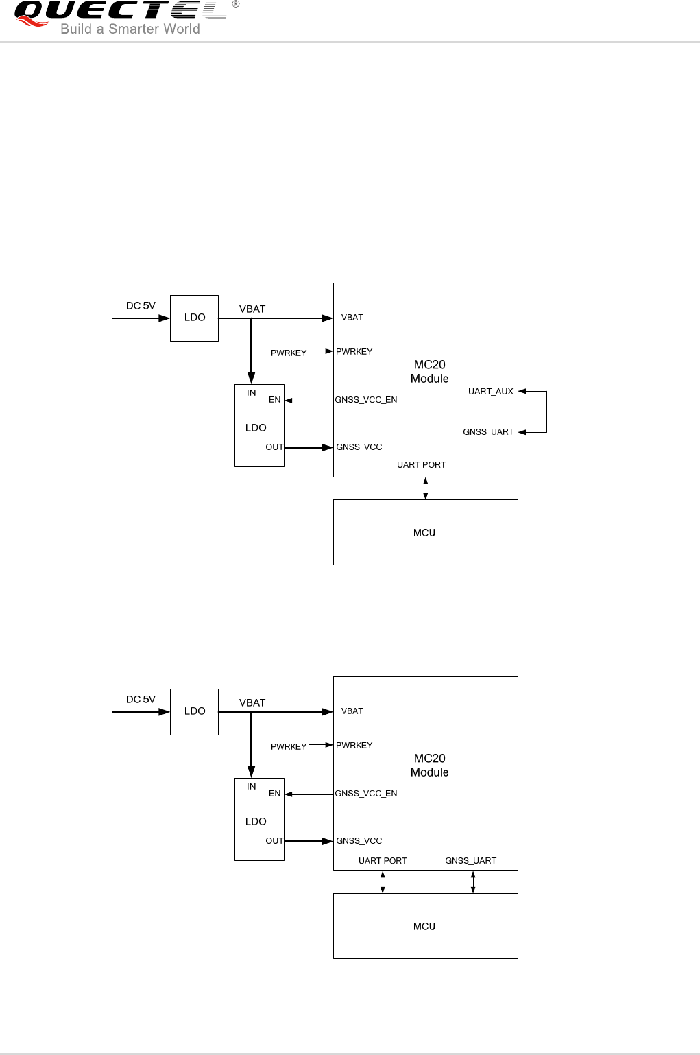
MC20 module integrates both GSM and GNSS engines which can work as a whole (all-in-one solution)
unit or work relatively independent (stand-alone solution) according to customer demands.
All-in-one solution allows for convenient communication between GSM and GNSS parts. The commands
and data (e.g. AT and PMTK commands, NMEA sentences output, etc.) in both GSM and GNSS parts are
Antenna Interface
PIN Name PIN No. I/O Description DC Characteristics Comment
RF_
ANT 41 IO GSM antenna pad Impedance of 50Ω
BT_
ANT 32 IO BT antenna pad Impedance of 50Ω If unused, keep
this pin open.
GNSS_
ANT 15 I GNSS signal input Impedance of 50Ω
Other Interface
PIN Name PIN No. I/O Description DC Characteristics Comment
GNSS_
VCC_EN 28 O GNSS power enabled
VOHmin=
0.85×VDD_EXT
VOLmax=
0.15×VDD_EXT
Refer to
Chapter 3.3.3.2
in all-in-one
solution.
Keep this pin
open in
stand-alone
solution.
RESERVED
17, 46
55, 56,
57, 58,
63, 64,
65, 66,
67, 68,
Keep these pins
open
PIN Name PIN No. Function After Reset Alternate Function
DTR/SIM1_PRESENCE 37 DTR SIM1_PRESENCE
GSM/GPRS/GNSS Module Series
MC20 Hardware Design
MC20_Hardware_Design Confidential / Released 26 / 95
transmitted through UART port, thus realizing communication between the module and the MCU.
In stand-alone solution, GSM data and AT commands are transmitted through UART port; while GNSS
data such as PMTK command and NMEA sentences output are transmitted through GNSS UART port.
The hardware difference between all-in-one solution and stand-alone solution mainly lies in the
connection method of UART, UART_AUX, and GNSS_UART. The corresponding schematic diagrams are
shown below.
Figure 3: All-in-one Solution Schematic Diagram
Figure 4: Stand-alone Solution Schematic Diagram

GSM/GPRS/GNSS Module Series
MC20 Hardware Design
MC20_Hardware_Design Confidential / Released 27 / 95
In order to ensure the normal operation of GNSS part, please don't power off the GSM part.
Table 8: Comparison between All-in-one and Stand-alone Solution
3.3. Power Supply
3.3.1. Power Features
The power supply of the GSM part is one of the key issues in MC20 module design. Due to the 577us
radio burst in GSM part every 4.615ms, the power supply must be able to deliver high current peaks in a
burst period. During these peaks, drops on the supply voltage must not exceed the minimum working
voltage of the GSM part.
The maximum current consumption of GSM part could reach 1.6A during a burst transmission. It will
cause a large voltage drop on the VBAT. In order to ensure stable operation of the part, it is
recommended that the maximum voltage drop during the burst transmission does not exceed 400mV.
All-in-one. Stand-alone Remarks
Firmware upgrade
Firmware upgrade via
UART Port (GSM and
GNSS Parts share the
same firmware package)
Firmware upgrade via
UART Port (GSM and
GNSS Parts share the
same firmware package)
Refer to Chapter
3.6.1.3 for details
Data transmission
Both GSM and GNSS data
are transmitted through
the GSM UART Port
GSM data is transmitted
through the GSM UART
Port.
GNSS data is transmitted
through the GNSS UART
Port.
GNSS wake up GSM GNSS can wake up GSM
by interrupts N/A
GNSS’s EPO data
download
EPO data is downloaded
directly through the GSM
part.
MCU receives the EPO
data which is downloaded
through the GSM part, and
then transmit it to the
GNSS part.
Refer to Chapter
3.13 for details
NOTE

GSM/GPRS/GNSS Module Series
MC20 Hardware Design
MC20_Hardware_Design Confidential / Released 28 / 95
Figure 5: Voltage Ripple during Transmitting (GSM Part)
The power supply for GNSS part is controlled by the GSM part through AT command control over
GNSS_VCC_EN pin.
3.3.2. Decrease Supply Voltage Drop
3.3.2.1. Decrease Supply Voltage Drop for GSM Part
Power supply range of the GSM part is from 3.3V to 4.6V. Make sure that the input voltage will never drop
below 3.3V even in a burst transmission. If the power voltage drops below 3.3V, the module will be turned
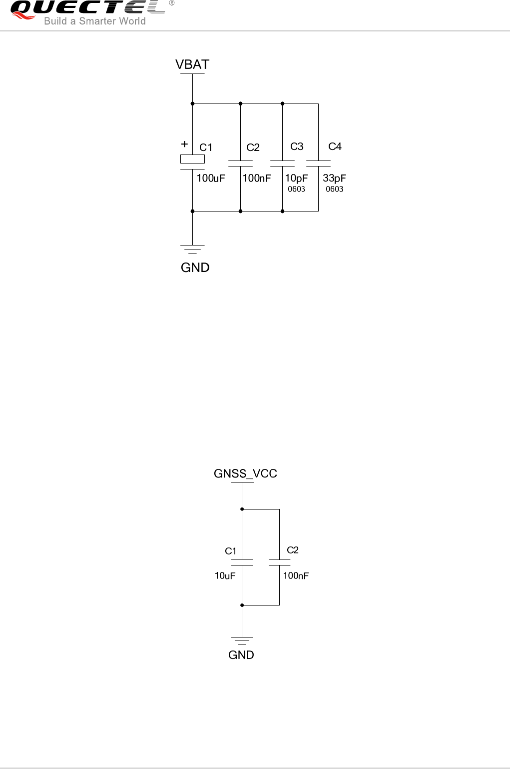
off automatically. For better power performance, it is recommended to place a 100uF tantalum capacitor
with low ESR (ESR=0.7Ω) and ceramic capacitors 100nF, 33pF and 10pF near the VBAT pin. A reference
circuit is illustrated in the following figure.
The VBAT trace should be wide enough to ensure that there is not too much voltage drop during burst
transmission. The width of trace should be no less than 2mm; and in principle, the longer the VBAT trace,
the wider it will be.
GSM/GPRS/GNSS Module Series
MC20 Hardware Design
MC20_Hardware_Design Confidential / Released 29 / 95
Figure 6: Reference Circuit for the VBAT Input (GSM Part)
3.3.2.2. Decrease Supply Voltage Drop for GNSS Part
Power supply range of GNSS part is from 2.8 to 4.3V. GNSS_VCC’s maximum average current is 40mA
during GNSS acquisition after power up. So it is important to supply sufficient current and make the power
clean and stable. The decouple combination of 10uF and 100nF capacitor is recommended nearby
GNSS_VCC pin. A reference circuit is illustrated in the following figure.
Figure 7: Reference Circuit for the GNSS_VCC Input
GSM/GPRS/GNSS Module Series
MC20 Hardware Design
MC20_Hardware_Design Confidential / Released 30 / 95
3.3.3. Reference Design for Power Supply
3.3.3.1. Reference Design for Power Supply of GSM Part
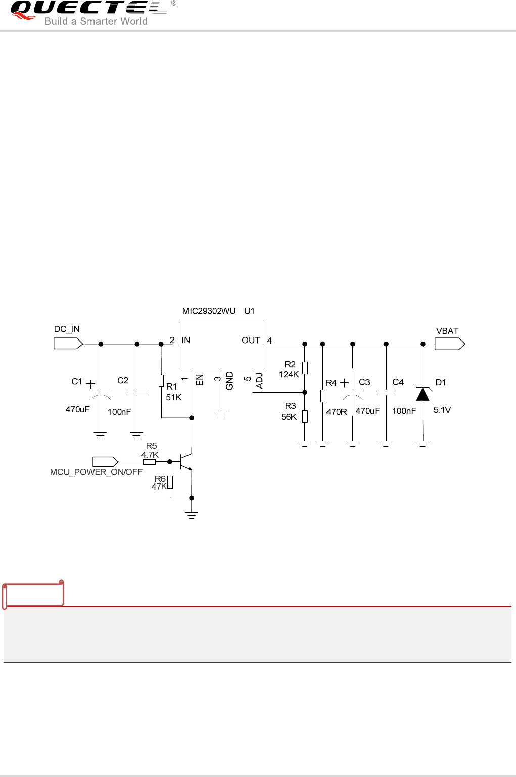
The power supply of GSM part is capable of providing sufficient current up to 2A at least. If the voltage
drop between the input and output is not too high, it is suggested to use a LDO as the GSM part’s power
supply. If there is a big voltage difference between the input source and the desired output (VBAT), a
switcher power converter is recommended to be used as the power supply.
The following figure shows a reference design for +5V input power source for GSM part. The designed
output for the power supply is 4.0V and the maximum load current is 3A. In addition, in order to get a
stable output voltage, a zener diode is placed close to the pins of VBAT. As to the zener diode, it is
suggested to use a zener diode whose reverse zener voltage is 5.1V and dissipation power is more than 1
Watt.
Figure 8: Reference Circuit for Power Supply of the GSM Part
It is suggested to control the module’s main power supply (VBAT) via LDO enable pin to restart the
module when the module becomes abnormal. Power switch circuit like P-channel MOSFET switch circuit
can also be used to control VBAT.
NOTE
GSM/GPRS/GNSS Module Series
MC20 Hardware Design
MC20_Hardware_Design Confidential / Released 31 / 95
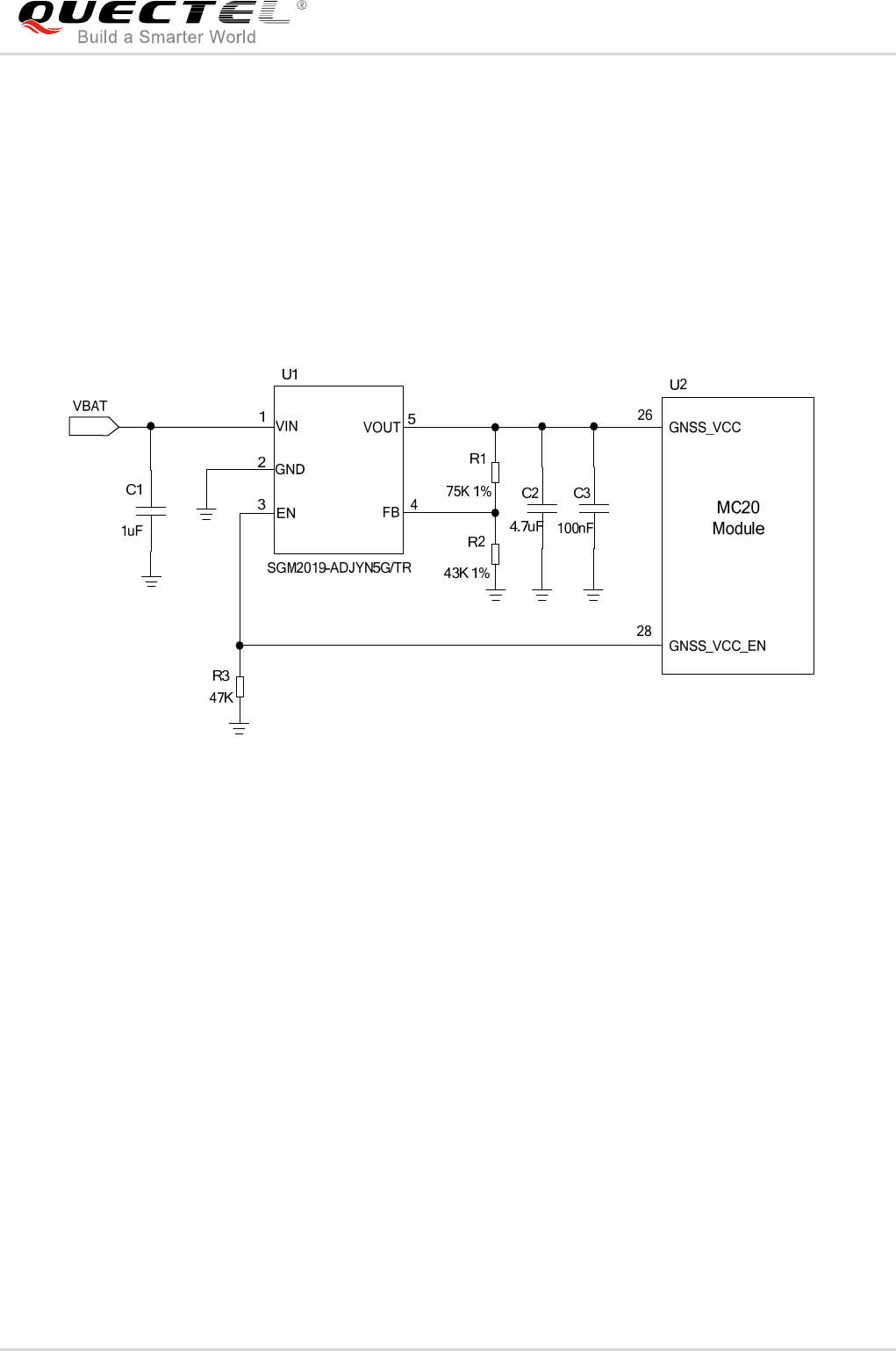
3.3.3.2. Reference Design for Power Supply of GNSS Part
The power supply for GNSS part is controlled by the GSM part through AT command control over
GNSS_VCC_EN pin.
A reference circuit for the GNSS part power supply is given below. Please pay attention to the electrical
characteristics of GNSS_VCC_EN to match LDO’s EN pin. Please refer to document [1] for details about
the AT commands for GNSS control.
Figure 9: Reference Circuit Design for GNSS Part
3.3.4. Monitor Power Supply
The command AT+CBC can be used to monitor the supply voltage of the GSM part. The unit of the
displayed voltage is mV.
For details, please refer to document [1].
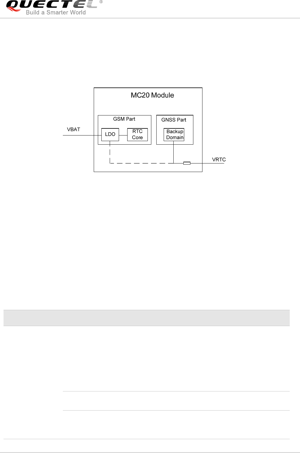
3.3.5. Backup Domain of GNSS
The GNSS part of MC20 module features a backup domain which contains all the necessary GNSS
information for quick start-up and a small amount of user configuration variables. In GNSS’s backup mode,
the backup domain is still alive. As long as the backup domain is alive, EASY technology will be available.
As the GNSS’s backup domain is powered by VBAT, the GNSS’s backup mode will be active as long as
the following conditions are satisfied at the same time:
GSM/GPRS/GNSS Module Series
MC20 Hardware Design
MC20_Hardware_Design Confidential / Released 32 / 95
The main power supply (VBAT) is remained
The GSM part is powered on
The GNSS part is turned off by AT+QGNSSC=0 command via UART
In this case, the VRTC pin can be kept floating. A reference schematic diagram is shown below.
Figure 10: Internal GNSS’s Backup Domain Power Construction
3.4. Operating Modes
3.4.1. Operating Modes of GSM Part
The table below briefly summarizes the various operating modes of GSM part mentioned in the following
chapters.
Table 9: Operating Modes Overview of GSM Part
Modes Function
GSM Normal
Operation
GSM/GPRS
Sleep
After enabling sleep mode by AT+QSCLK=1, the GSM part will
automatically enter into Sleep Mode if DTR is set to high level
and there is no interrupt (such as GPIO interrupt or data on
UART port). In this case, the current consumption of the GSM
part will reduce to the minimal level.
During Sleep Mode, the GSM part can still receive paging
message and SMS from the system normally.
GSM IDLE Software is active. The GSM part has registered on GSM
network, and it is ready to send and receive GSM data.
GSM TALK
GSM connection is ongoing. In this mode, the power
consumption is decided by the configuration of Power Control
Level (PCL), dynamic DTX control and the working RF band.

GSM/GPRS/GNSS Module Series
MC20 Hardware Design
MC20_Hardware_Design Confidential / Released 33 / 95
Based on system requirements, there are several actions to drive the GSM part to enter into low current
consumption status. For example, AT+CFUN can be used to set the part into minimum functionality mode,
and DTR hardware interface signal can be used to lead the system to Sleep Mode.
3.4.1.1. Minimum Functionality Mode
Minimum functionality mode reduces the functionality of the GSM part to a minimum level. The
consumption of the current can be minimized when the slow clocking mode is activated at the same time.
The mode is set via the AT+CFUN command which provides the choice of the functionality levels
<fun>=0, 1, 4.
0: minimum functionality
1: full functionality (default)
4: disable from both transmitting and receiving RF signals
If the GSM part is set to minimum functionality by AT+CFUN=0, the RF function and SIM card function
would be disabled. In this case, the UART port is still accessible, but all AT commands related with RF
function or SIM card function will be unavailable.
If the GSM part is set by the command AT+CFUN=4, the RF function will be disabled, but the UART port
is still active. In this case, all AT commands related with RF function will be unavailable.
GPRS IDLE The GSM part is not registered on GPRS network. It is not
reachable through GPRS channel.
GPRS
STANDBY
The GSM part is registered on GPRS network, but no GPRS
PDP context is active. The SGSN knows the Routing Area
where the module is located at.
GPRS READY
The PDP context is active, but no data transfer is ongoing. The
GSM part is ready to receive or send GPRS data. The SGSN
knows the cell where the module is located at.
GPRS DATA
There is GPRS data in transfer. In this mode, power
consumption is decided by the PCL, working RF band and
GPRS multi-slot configuration.
POWER DOWN
Normal shutdown by sending the AT+QPOWD=1 command or using the
PWRKEY pin. The power management ASIC disconnects the power supply from
the base band part of the GSM part. Software is not active. The UART interfaces
are not accessible. Operating voltage (connected to VBAT) remains applied.
Minimum
Functionality Mode
(without removing
power supply)
AT+CFUN command can set the GSM part to a minimum functionality mode
without removing the power supply. In this case, the RF part of the GSM part will
not work or the SIM card will not be accessible, or both RF part and SIM card will
be disabled; but the UART port is still accessible. The power consumption in this
case is very low.

GSM/GPRS/GNSS Module Series
MC20 Hardware Design
MC20_Hardware_Design Confidential / Released 34 / 95
After the GSM part is set by AT+CFUN=0 or AT+CFUN=4, it can return to full functionality mode by
AT+CFUN=1.
For detailed information about AT+CFUN, please refer to document [1].
3.4.1.2. SLEEP Mode
SLEEP mode is disabled by default. It can be enabled by AT+QSCLK=1 and the premise is that the
GNSS is powered off. The default setting is AT+QSCLK=0, and in this mode, the GSM part cannot enter
SLEEP mode.
When the GSM part is set by the command AT+QSCLK=1, you can control the part to enter into or exit
from the SLEEP mode through pin DTR. When DTR is set to high level, and there is no on-air or hardware
interrupt such as GPIO interrupt or data on UART port, the GSM part will enter into SLEEP mode
automatically. In this mode, the GSM part can still receive voice, SMS or GPRS paging from network, but
the UART port does not work.
3.4.1.3. Wake up GSM Part from SLEEP Mode
When the GSM part is in the SLEEP mode, it can be woken up through the following methods:
If the DTR Pin is set low, it would wake up the GSM part from the SLEEP mode. The UART port will
be active within 20ms after DTR is changed to low level.
Receiving a voice or data call from network wakes up the GSM part.
Receiving an SMS from network wakes up the GSM part.
DTR pin should be held at low level during communication between the GSM part and the DTE.
3.4.2. Operating Modes of GNSS Part
3.4.2.1. Full on Mode
Full on mode includes tracking mode and acquisition mode. Acquisition mode is defined as that the GNSS
part starts to search satellites, and to determine the visible satellites, coarse carrier frequency & code
phase of satellite signals. When the acquisition is completed, it switches to tracking mode automatically.
Tracking mode is defined as that the GNSS part tracks satellites and demodulates the navigation data
NOTE
GSM/GPRS/GNSS Module Series
MC20 Hardware Design
MC20_Hardware_Design Confidential / Released 35 / 95
from specific satellites.
When the GNSS_VCC is valid, the GNSS part will enter into full on mode automatically. The following
table describes the default configuration of full on mode.
Table 10: Default Configuration of Full on Mode (GNSS Part)
Item Configuration Comment
Baud Rate 115200bps
Protocol NMEA RMC, VTG, GGA, GSA, GSV and GLL
Update Rate 1Hz
SBAS Enable
AIC Enable
LOCUS Disable
Easy Technology Enable EASY will be disabled automatically when update
rate exceeds 1Hz.
GNSS GPS+BeiDou
In full on mode, the consumption complies with the following regulations:
When the GNSS part is powered on, the average current will rush to 40mA and last for a few seconds;
then the consumption will be decreased to the acquisition current marked in table 3 and we defined this
state as acquisition state, and also it will last for several minutes until it switches to tracking state
automatically. The consumption in tracking state is less than that in acquisition state. The value is also
listed in table 3.
Sending PMTK commands allows for switching among multiple positioning systems:
$PMTK353,0,0,0,0,1*2A: search BDS satellites only
$PMTK353,1,0,0,0,0*2A: search GPS satellites only
$PMTK353,1,0,0,0,1*2B: search GPS and BDS satellites
In all-in-one solution, make sure the GNSS part is powered on before sending these PMTK commands.
NOTE

GSM/GPRS/GNSS Module Series
MC20 Hardware Design
MC20_Hardware_Design Confidential / Released 36 / 95
3.4.2.2. Standby Mode
Standby mode is a low-power consumption mode. In standby mode, the internal core and I/O power
domain are still active; but RF and TCXO are powered off, and the GNSS part stops satellites search and
navigation. The way to enter into standby mode is using PMTK commands.
When the GNSS part exits from standby mode, it will use all internal aiding information like GNSS time,
ephemeris, last position, etc., to ensure the fastest possible TTFF in either Hot or Warm start. The typical
current consumption is about 300uA @GNSS_VCC=3.3V in standby mode.
Sending the following PMTK command can make GNSS part enter into standby mode:
$PMTK161,0*28: make sure the GNSS part is powered on before sending the command in
all-in-one solution.
The following methods will make GNSS part exit from standby mode:
Sending any data via UART will make GNSS part exit from standby mode in all-in-one solution.
Sending any data via GNSS_UART will make GNSS part exit from standby mode in stand-alone
solution.
3.4.2.3. Backup Mode
Backup mode requires lower power consumption than standby mode. In this mode, the GNSS part stops
acquiring and tracking satellites, but the backed-up memory in backup domain which contains all the
necessary GNSS information for quick start-up and a small amount of user configuration variables is alive.
As long as the backup domain is alive, EASY technology is available. The current consumption in this
mode is about 14uA.
The following method will make GNSS part enter into backup mode:
When VBAT is kept powered and the GSM part is powered on, sending AT+QGNSSC=0 will make
GNSS part enter into backup mode from full on mode.
The following method will make GNSS part exit from backup mode:
Sending AT+QGNSSC=1 via UART, the GNSS part will exit from backup mode and enter full on
mode immediately.
In order to enable GNSS part working in backup mode, please make sure the GSM part is powered on.
NOTE
GSM/GPRS/GNSS Module Series
MC20 Hardware Design
MC20_Hardware_Design Confidential / Released 37 / 95
3.4.3. Summary of GSM and GNSS Parts’ State in All-in-one Solution
Table 11: Combination States of GSM and GNSS Parts in All-in-one Solution
GSM Part Modes GNSS Part Modes
Full on Standby Backup
Normal
Sleep
Minimum Functionality
3.4.4. Summary of GSM and GNSS Parts’ State in Stand-alone Solution
Table 12: Combination States of GSM and GNSS Parts in Stand-alone Solution
GSM Part Modes GNSS Part Modes
Full on Standby Backup
Normal
Sleep
Minimum Functionality
1. The mark means that the Part supports this mode.
2. In all-in-one solution, all PMTK commands used for the GNSS part should be sent through the GSM
UART after the GNSS part is powered on. Make sure the GSM UART Port is accessible.
3. In all-in-one solution, when the GSM part is in sleep mode, the GNSS part can work in either standby
or full on mode. However, if NMEA GPS data is needed, the GSM part should be woken up first and
then send the corresponding AT command to get. For detailed AT command information, please refer
to document [1].
4. In stand-alone solution, all PMTK commands used for the GNSS part or NMEA output can be sent or
received through GNSS UART port when the GSM part is powered on.
NOTES
GSM/GPRS/GNSS Module Series
MC20 Hardware Design
MC20_Hardware_Design Confidential / Released 38 / 95
3.5. Power on and down
3.5.1. Power on
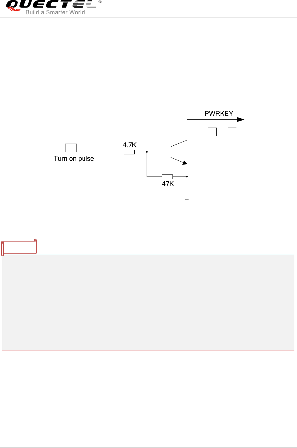
The module can be turned on by driving the pin PWRKEY to a low level voltage. An open collector driver
circuit is suggested to control the PWRKEY. A simple reference circuit is illustrated as below.
Figure 11: Turn on the Module with an Open-collector Driver
1. MC20 module is set to autobauding mode (AT+IPR=0) by default. In autobauding mode, URC RDY is
not reported to the host controller after the module is powered on. When the module is powered on after
a delay of 4 or 5 seconds, it can receive AT commands. Host controller should first send an AT string in
order that the module can detect baud rate of host controller, and it should continue to send the next AT
string until receiving OK string from the module. Then enter AT+IPR=x;&W to set a fixed baud rate for
the module and save the configuration to flash memory of the module. After these configurations, the
URC RDY would be received from the UART Port of the module every time when the module is
powered on. For more details, refer to the section AT+IPR in document [1].
2. When AT command is responded, it indicates the module is turned on successfully; or else the module
fails to be turned on.
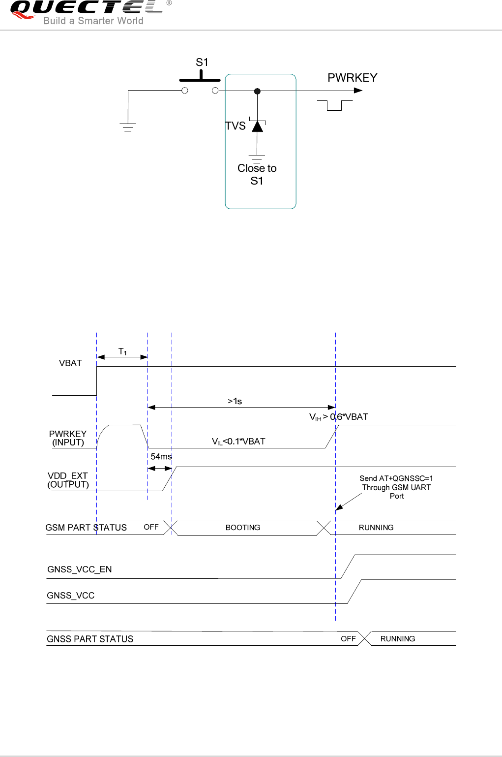
The other way to control the PWRKEY is through a button directly. While pressing the key, electrostatic
strike may generate from the finger, and thus, a TVS component is indispensable to be placed nearby the
button for ESD protection. For the best performance, the TVS component must be placed nearby the
button. A reference circuit is shown in the following figure.
NOTES
GSM/GPRS/GNSS Module Series
MC20 Hardware Design
MC20_Hardware_Design Confidential / Released 39 / 95
Figure 12: Turn on the Module with a Button
Command AT+QGNSSC=1 should be sent to enable the GNSS power supply after the GSM part is
running. When the GNSS_VCC is valid, the GNSS will enter into full on mode automatically. The turn-on
timing is illustrated in the following figure.
Figure 13: Turn-on Timing
GSM/GPRS/GNSS Module Series
MC20 Hardware Design
MC20_Hardware_Design Confidential / Released 40 / 95
3.5.2. Power down
The following procedures can be used to turn off the module:
Normal power down procedure: Turn off module using the PWRKEY pin
Normal power down procedure: Turn off module using command AT+QPOWD
Under-voltage automatic shutdown: Take effect when under-voltage is detected.
3.5.2.1. Power down Module Using the PWRKEY Pin
It is a safe way to turn off the module by driving the PWRKEY to a low level voltage for a certain time. The
power down scenario is illustrated in the following figure.
The power down procedure causes the module to log off from the network and allows the firmware to
save important data before completely disconnecting the power supply.
Before the completion of the power down procedure, the module sends out the result code shown below:
NORMAL POWER DOWN
1. When unsolicited result codes do not appear when autobauding is active and DTE & DCE are not
correctly synchronized after start-up, the module is recommended to be set to a fixed baud rate.
2. As network logout time is related to the local mobile network, it is recommended to delay about 12
seconds before disconnecting the power supply or restarting the module.
After that moment, no further AT commands can be executed. Then the module enters the power down
mode.
Make sure that VBAT is stable before pulling down PWRKEY pin. The time of T1 is recommended to be
100ms.
NOTE
NOTES
GSM/GPRS/GNSS Module Series
MC20 Hardware Design
MC20_Hardware_Design Confidential / Released 41 / 95
Figure 14: Turn-off Timing by Using the PWRKEY Pin
3.5.2.2. Power down Module Using AT Command
It is also a safe way to turn off the module via AT command AT+QPOWD=1. This command will let the
module log off from the network and allow the firmware to save important data before completely
disconnecting the power supply.
Before the completion of the power down procedure, the module sends out the result code shown below:
NORMAL POWER DOWN
After that moment, no further AT commands can be executed. And then the module enters into the power
down mode.
Please refer to document [1] for details about the AT command AT+QPOWD.
GSM/GPRS/GNSS Module Series
MC20 Hardware Design
MC20_Hardware_Design Confidential / Released 42 / 95
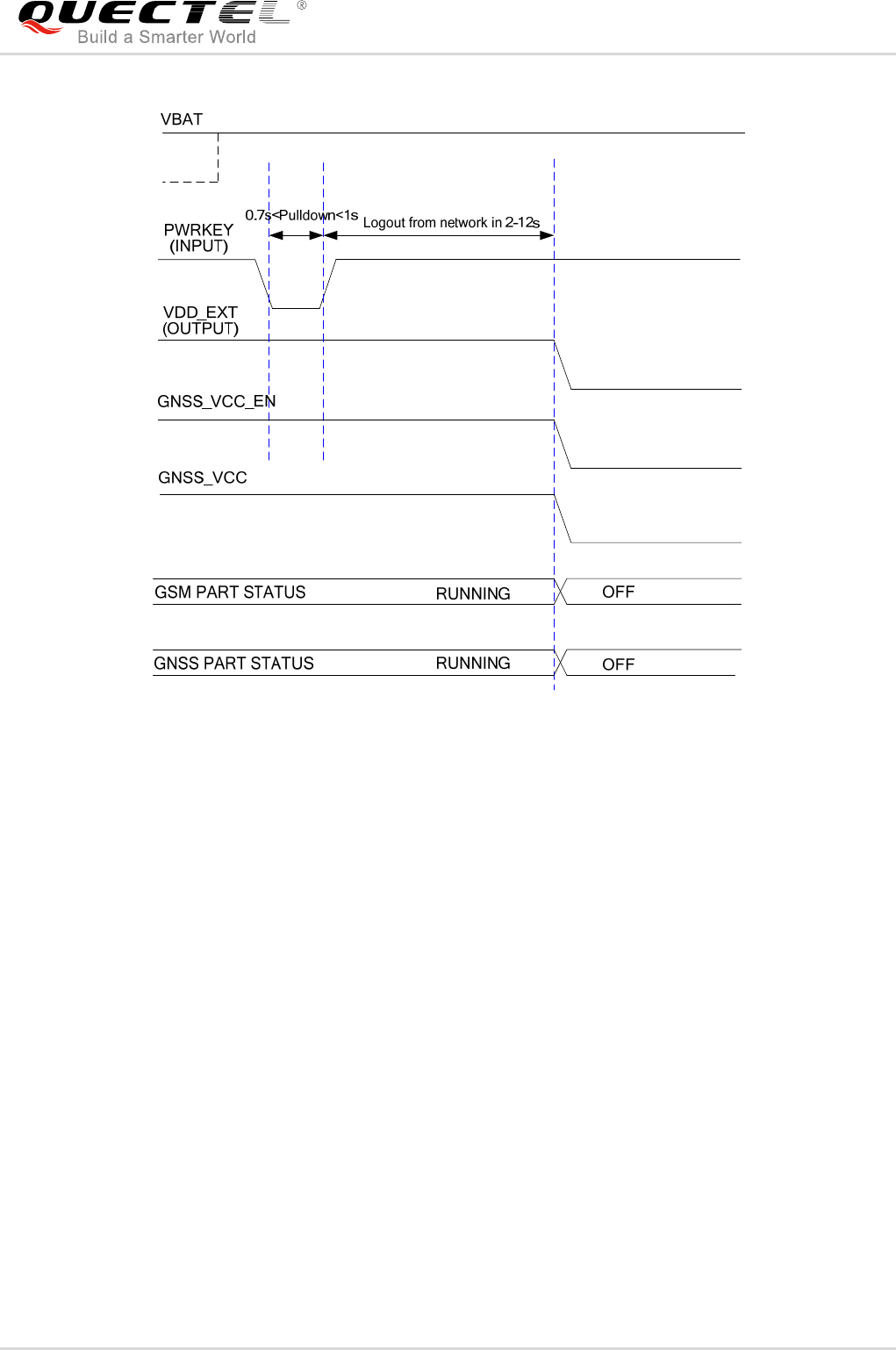
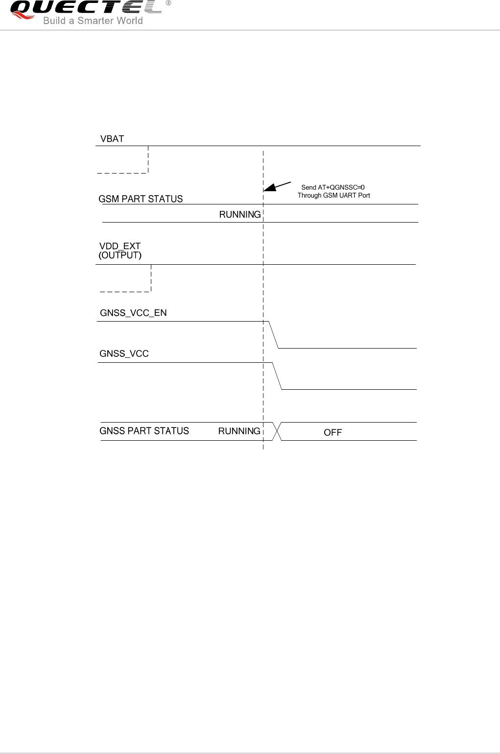
3.5.2.3. Power down GNSS Part Alone Using AT Command
It is a safe way to turn off the GNSS part alone via AT command AT+QGNSSC=0. The power down
scenario for GNSS part is illustrated in the following figure.
Figure 15: Turn-off Timing of GNSS Part by Using AT Command
3.5.2.4. Under-voltage Automatic Shutdown
The module will constantly monitor the voltage applied on the VBAT. If the voltage is ≤3.5V, the following
URC will be presented:
UNDER_VOLTAGE WARNING
The normal input voltage range is from 3.3V to 4.6V. If the voltage is <3.3V, the module will automatically
shut down.
If the voltage is <3.3V, the following URC will be presented:

GSM/GPRS/GNSS Module Series
MC20 Hardware Design
MC20_Hardware_Design Confidential / Released 43 / 95
UNDER_VOLTAGE POWER DOWN
After that moment, no further AT commands can be executed. The module logs off from network and
enters into power down mode.
When unsolicited result codes do not appear when autobauding is active and DTE & DCE are not
correctly synchronized after start-up, the module is recommended to be set to a fixed baud rate.
3.6. Serial Interfaces
The module provides four serial ports: UART Port, Debug Port, Auxiliary UART Port and GNSS UART
Port. The module is designed as DCE (Data Communication Equipment), following the traditional
DCE-DTE (Data Terminal Equipment) connection. Autobauding function supports baud rate from
4800bps to 115200bps.
The UART Port:
TXD: Send data to RXD of DTE.
RXD: Receive data from TXD of DTE.
RTS: Request to send.
CTS: Clear to send.
DTR: DTE is ready and inform DCE (this pin can wake the module up).
RI: Ring indicator (when there is a call, SMS or URC output, the module will inform DTE with the RI
pin).
DCD: Data carrier detection (the validity of this pin demonstrates successful set-up of the
communication link).
The Debug Port:
DBG_TXD: Send data to the COM port of peripheral.
DBG_RXD: Receive data from the COM port of peripheral.
The Auxiliary UART Port:
In all-in-one solution:
TXD_AUX: Send data to the GNSS part.
RXD_AUX: Receive data from the GNSS part.
In stand-alone solution:
TXD_AUX: Keep open except during firmware upgrade.
NOTE

GSM/GPRS/GNSS Module Series
MC20 Hardware Design
MC20_Hardware_Design Confidential / Released 44 / 95
RXD_AUX: Keep open except during firmware upgrade.
The GNSS UART Port
In all-in-one solution:
GNSS_TXD: Send data to the GSM part.
GNSS_RXD: Receive data from the GSM part.
In stand-alone solution:
GNSS_TXD: Send GNSS data to the COM port of peripheral.
GNSS_RXD: Receive GNSS data from the COM port of peripheral.
The logic levels are described in the following table.
Table 13: Logic Levels of the UART Interface
Table 14: Pin Definition of the UART Interfaces
Parameter Min. Max. Unit
VIL 0 0.25×VDD_EXT V
VIH 0.75×VDD_EXT VDD_EXT +0.2 V
VOL 0 0.15×VDD_EXT V
VOH 0.85×VDD_EXT VDD_EXT V
Interface Pin Name Pin No. Description
UART Port
TXD 34 Transmit data
RXD 33 Receive data
DTR 37 Data terminal ready
RI 35 Ring indication
DCD 36 Data carrier detection
CTS 38 Clear to send
RTS 39 Request to send
Debug Port DBG_RXD 30 Receive data

GSM/GPRS/GNSS Module Series
MC20 Hardware Design
MC20_Hardware_Design Confidential / Released 45 / 95
1) It is recommended to keep these pins open in stand-alone solution, except during firmware upgrade.
3.6.1. UART Port
3.6.1.1. Features of UART Port
Seven lines on UART interface
Contain data lines TXD and RXD, hardware flow control lines RTS and CTS, as well as other control
lines DTR, DCD and RI.
Used for AT command, GPRS data, etc. Multiplexing function is supported on the UART Port. NMEA
output and PMTK command can be supported in all-in-one solution.
Support the following communication baud rates:
300, 600, 1200, 2400, 4800, 9600, 14400, 19200, 28800, 38400, 57600, 115200bps.
The default setting is autobauding mode. Support the following baud rates for autobauding function:
4800, 9600, 19200, 38400, 57600, 115200bps.
Hardware flow control is disabled by default. When hardware flow control is required, RTS and CTS
should be connected to the host. AT command AT+IFC=2,2 is used to enable hardware flow control.
AT command AT+IFC=0,0 is used to disable the hardware flow control. For more details, please refer
to document [1].
After setting a fixed baud rate or autobauding, please send “AT” string at that rate. The UART port is
ready when it responds “OK”.
Autobauding allows the module to detect the baud rate by receiving the string “AT” or “at” from the host or
PC automatically, which gives module flexibility without considering which baud rate is used by the host
controller. Autobauding is enabled by default. To take advantage of the autobauding mode, special
attention should be paid according to the following requirements:
DBG_TXD 29 Transmit data
Auxiliary UART Port1)
RXD_AUX1) 24 Receive data
TXD_AUX
1) 25 Transmit data
GNSS UART Port
GNSS_RXD 23 Receive data
GNSS_TXD 22 Transmit data
NOTE
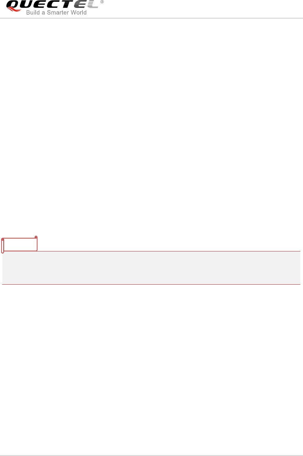
GSM/GPRS/GNSS Module Series
MC20 Hardware Design
MC20_Hardware_Design Confidential / Released 46 / 95
Synchronization between DTE and DCE:
When DCE (the module) is powered on with autobauding enabled, it is recommended to wait 2 to 3
seconds before sending the first AT character. After receiving the “OK” response, DTE and DCE are
correctly synchronized.
If the host controller needs URC in the mode of autobauding, it must be synchronized firstly. Otherwise
the URC will be discarded.
Restrictions on autobauding operation:
The UART port has to be operated at 8 data bits, no parity and 1 stop bit (factory setting).
The “At” and “aT” commands cannot be used.
Only the strings “AT” or “at” can be detected (neither “At” nor “aT”).
The Unsolicited Result Codes like RDY, +CFUN: 1 and +CPIN: READY will not be indicated when
the module is turned on with autobauding enabled and not be synchronized.
Any other Unsolicited Result Codes will be sent at the previous baud rate before the module detects
the new baud rate by receiving the first “AT” or “at” string. The DTE may receive unknown characters
after switching to a new baud rate.
It is not recommended to switch to autobauding from a fixed baud rate.
If autobauding is active it is not recommended to switch to multiplex mode.
To assure reliable communication and avoid any problems caused by undetermined baud rate between
DCE and DTE, it is strongly recommended to configure a fixed baud rate and save it instead of using
autobauding after start-up. For more details, please refer to the Section AT+IPR in document [1].
3.6.1.2. The Connection of UART
The connection between module and host using UART Port is very flexible. Three connection styles are
illustrated as below.
A reference design for Full-Function UART connection is shown as below when it is applied in
modulation-demodulation.
NOTE
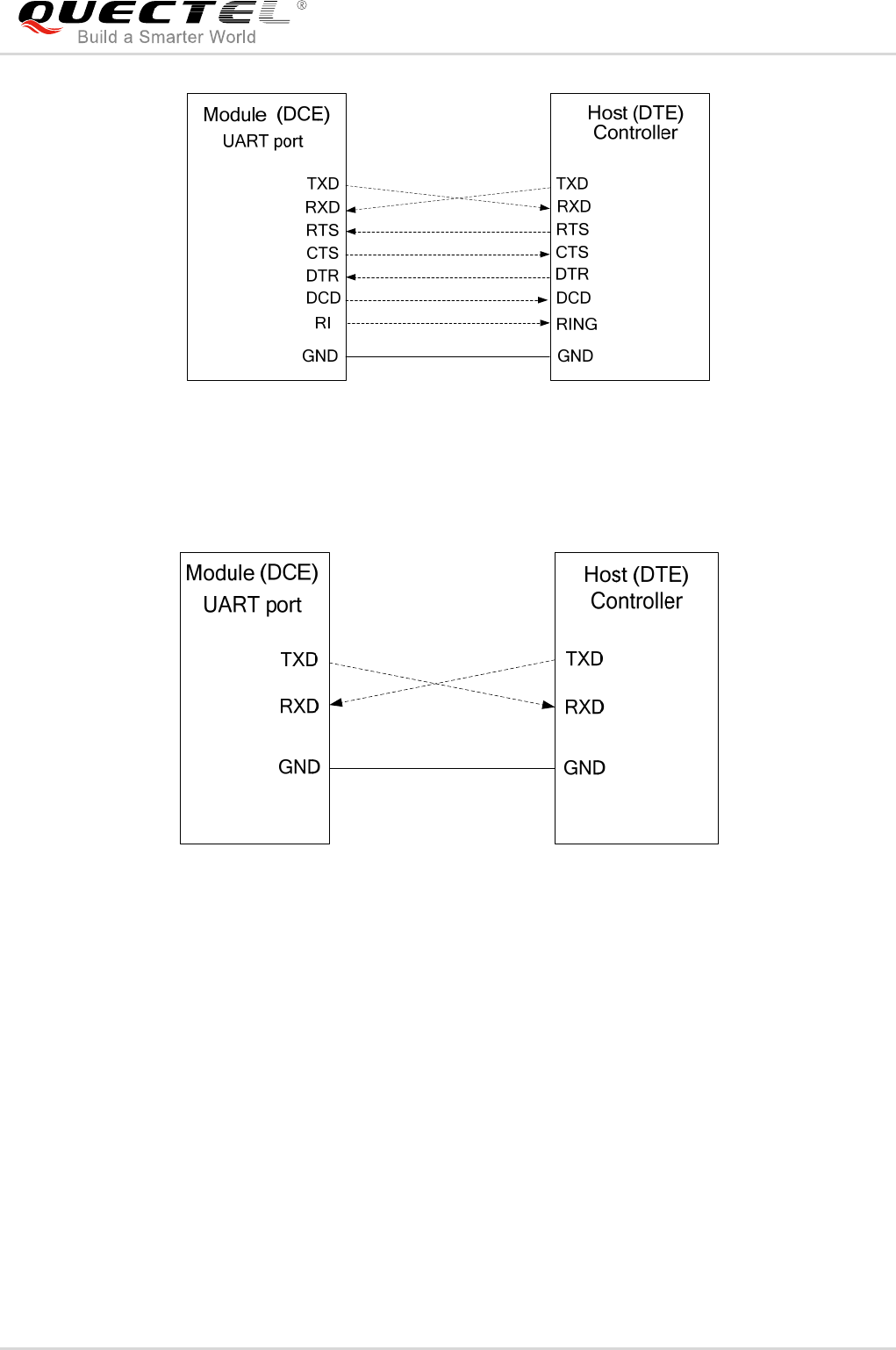
GSM/GPRS/GNSS Module Series
MC20 Hardware Design
MC20_Hardware_Design Confidential / Released 47 / 95
Figure 16: Reference Design for Full-Function UART
Three-line connection is shown as below.
Figure 17: Reference Design for UART Port (Three Line Connection)
A reference design for UART Port with hardware flow control is shown as below. The connection will
enhance the reliability of the mass data communication.
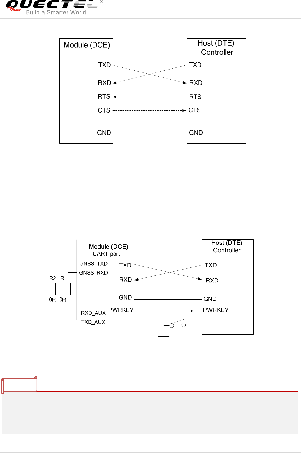
GSM/GPRS/GNSS Module Series
MC20 Hardware Design
MC20_Hardware_Design Confidential / Released 48 / 95
Figure 18: Reference Design for UART Port with Hardware Flow Control
3.6.1.3. Firmware Upgrade
TXD and RXD can be used for firmware upgrade in both all-in-one solution and stand-alone solution.
The PWRKEY pin must be pulled down before firmware upgrade. A reference circuit is shown as below:
Figure 19: Reference Design for Firmware Upgrade
1. In stand-alone solution, make sure the Auxiliary UART Port is connected to the GNSS UART Port
during firmware upgrade. Please refer to Chapter 3.6.3.2 for details.
2. The firmware of module might need to be upgraded due to a certain reasons. It is thus recommended
to reserve these pins in the host board for firmware upgrade.
NOTES
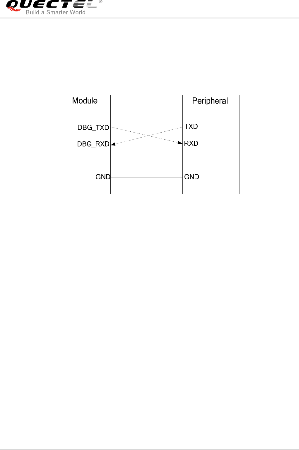
GSM/GPRS/GNSS Module Series
MC20 Hardware Design
MC20_Hardware_Design Confidential / Released 49 / 95
3.6.2. Debug Port
Two lines: DBG_TXD and DBG_RXD.
The port outputs log information automatically.
Debug Port is only used for firmware debugging and its baud rate must be configured as 460800bps.
Figure 20: Reference Design for Debug Port
3.6.3. Auxiliary UART Port and GNSS UART Port
3.6.3.1. Connection in All-in-one Solution
In all-in-one solution, the Auxiliary UART Port and GNSS UART Port should be connected together, thus
allowing for communication between GSM and GNSS parts. A reference design is shown below.
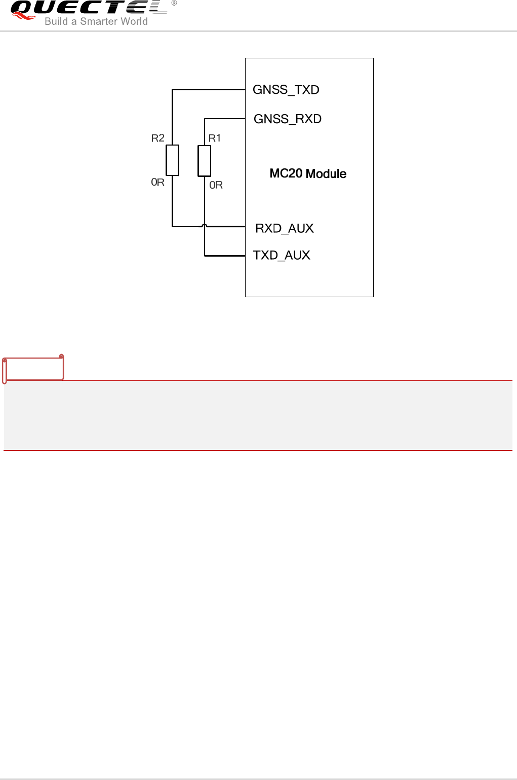
GSM/GPRS/GNSS Module Series
MC20 Hardware Design
MC20_Hardware_Design Confidential / Released 50 / 95
Figure 21: Auxiliary and GNSS UART Port Connection in All-in-one Solution
As the GNSS part of MC20 module outputs more data than a single GNSS system, the default output
NMEA types running in 4800bps baud rate and 1Hz update rate will lose some data. The solution to avoid
losing data in 4800bps baud rate and 1Hz update rate is to decrease the output NMEA types. 115200bps
baud rate is enough to transmit GNSS NMEA in default settings and it is thus recommended.
3.6.3.2. Connection in Stand-alone Solution
In stand-alone solution, the GNSS UART Port is connected to the COM port of peripheral. During
firmware upgrade, switch S1 should be kept closed. Otherwise, it should be kept open. A reference design
is shown below.
NOTE
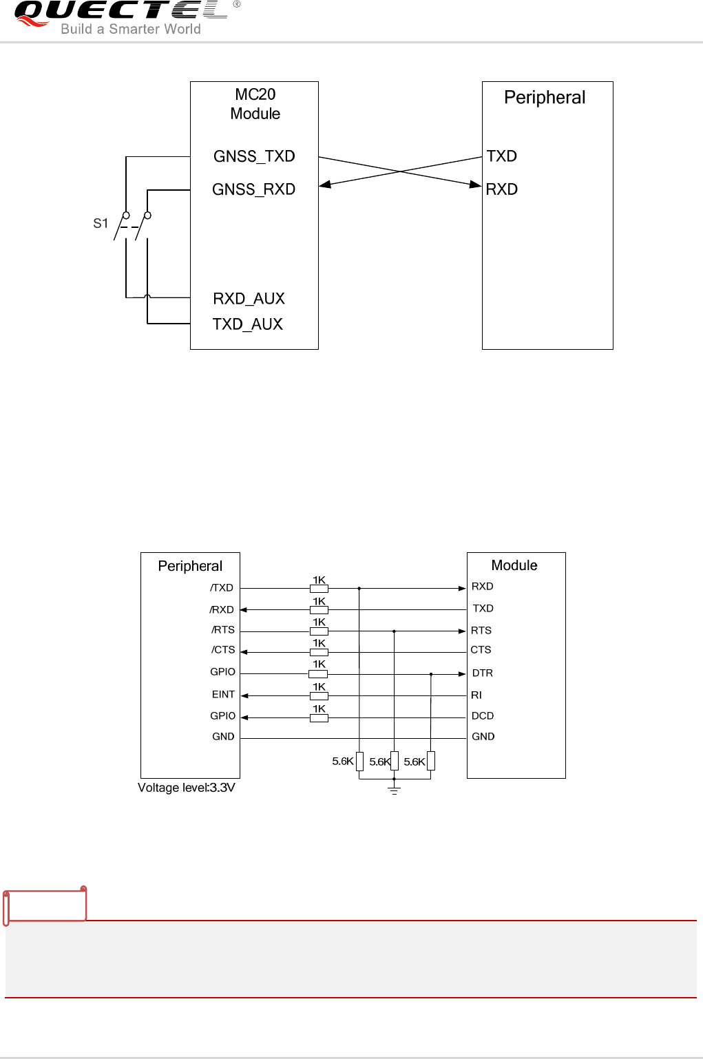
GSM/GPRS/GNSS Module Series
MC20 Hardware Design
MC20_Hardware_Design Confidential / Released 51 / 95
Figure 22: Auxiliary and GNSS UART Port Connection in Stand-alone Solution
3.6.4. UART Application
A reference design of 3.3V level match is shown as below. If the host is a 3V system, please change the
5.6K resistors to 10K ones.
Figure 23: Level Match Design for 3.3V System
It is highly recommended to add the resistor divider circuit on the UART signal lines when the host’s level
is 3V or 3.3V. For a higher voltage level system, a level shifter IC could be used between the host and the
module. For more details about UART circuit design, please refer to document [13].
NOTE
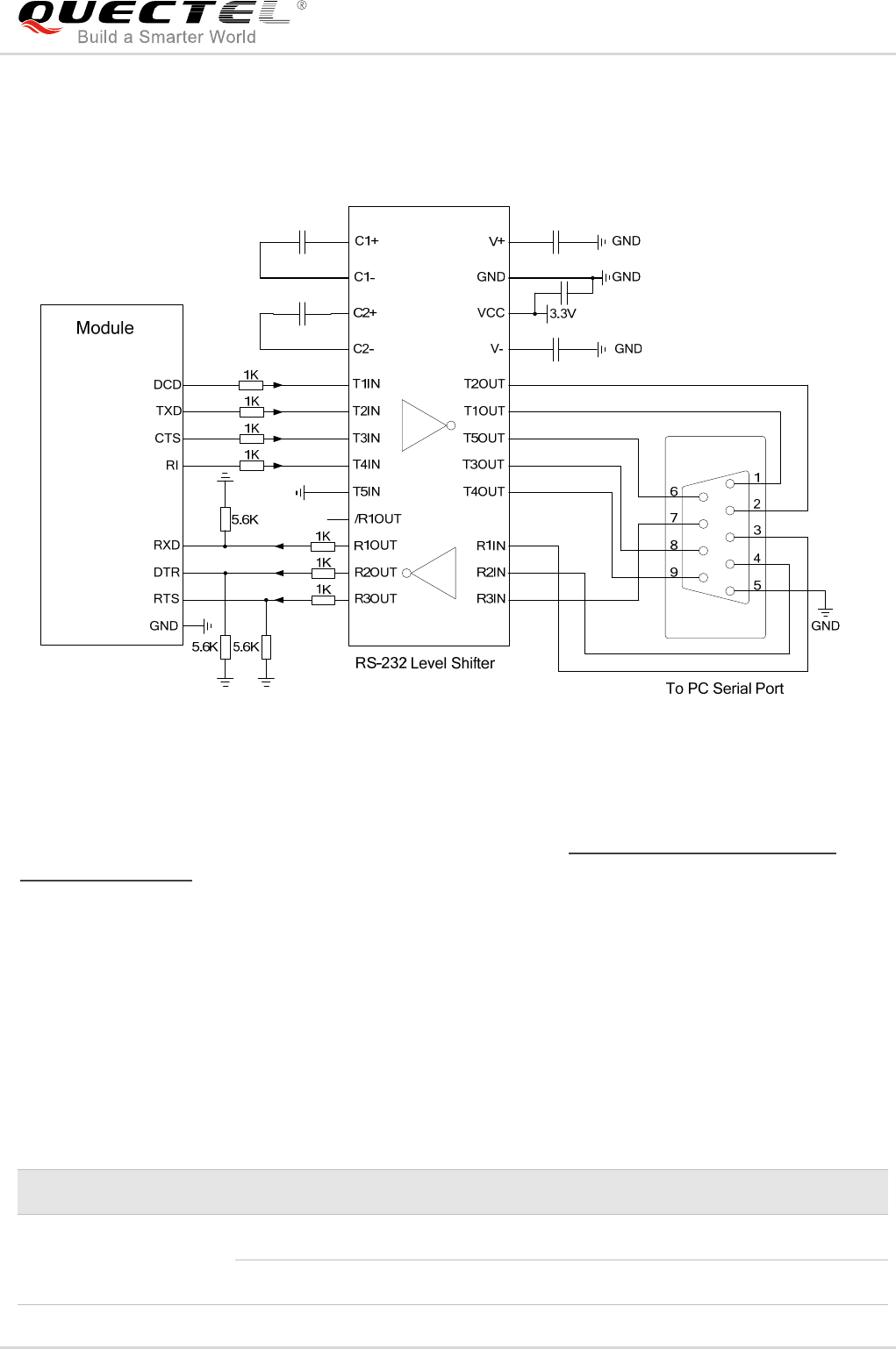
GSM/GPRS/GNSS Module Series
MC20 Hardware Design
MC20_Hardware_Design Confidential / Released 52 / 95
The following figure shows a sketch map between the module and the standard RS-232 interface. As the
electrical level of module is 2.8V, a RS-232 level shifter must be used. Note that you should assure the
I/O voltage of level shifter which connects to module is 2.8V.
Figure 24: Sketch Map for RS-232 Interface Match
Please visit vendors’ websites to select a suitable IC, such as: http://www.maximintegrated.com and
http://www.exar.com/.
3.7. Audio Interfaces
The module provides one analog input channel and two analog output channels.
Table 15: Pin Definition of Audio Interface
Interface Pin Name Pin No. Description
AIN/AOUT1
MICP 1 Microphone positive input
MICN 2 Microphone negative input

GSM/GPRS/GNSS Module Series
MC20 Hardware Design
MC20_Hardware_Design Confidential / Released 53 / 95
AIN can be used for input of microphone and line. An electret microphone is usually used. AIN are
differential input channels.
AOUT1 is used for output of receiver. The channel is typically used for building a receiver into a handset.
AOUT1 channel is a differential channel.
AOUT2 is used for loudspeaker output as it is embedded with an amplifier of class AB whose maximum
drive power is 800mW. AOUT2 is a differential channel.
AOUT2 also can be used for output of earphone, and can be used as a single-ended channel.
All these audio channels support voice and ringtone output, and so on, and can be switched by
AT+QAUDCH command. For more details, please refer to document [1].
Use AT command AT+QAUDCH to select audio channel:
0--AIN/AOUT1, the default value is 0.
1--AIN/AOUT2, this channel is always used for earphone.
2--AIN/AOUT2, this channel is always used for loudspeaker.
For each channel, you can use AT+QMIC to adjust the input gain level of microphone. You can also use
AT+CLVL to adjust the output gain level of receiver and speaker. AT+QSIDET is used to set the
side-tone gain level. For more details, please refer to document [1].
Table 16: AOUT2 Output Characteristics
SPKP 3 Channel 1 Audio positive output
SPKN 4 Channel 1 Audio negative output
AIN/AOUT2
MICP 1 Microphone positive input
MICN 2 Microphone negative input
LOUDSPKP 54 Channel 2 Audio positive output
LOUDSPKN 53 Channel 2 Audio negative output
Item Condition Min. Typ. Max. Unit
RMS Power
8ohm load
VBAT=3.7v
THD+N=1%
800 mW
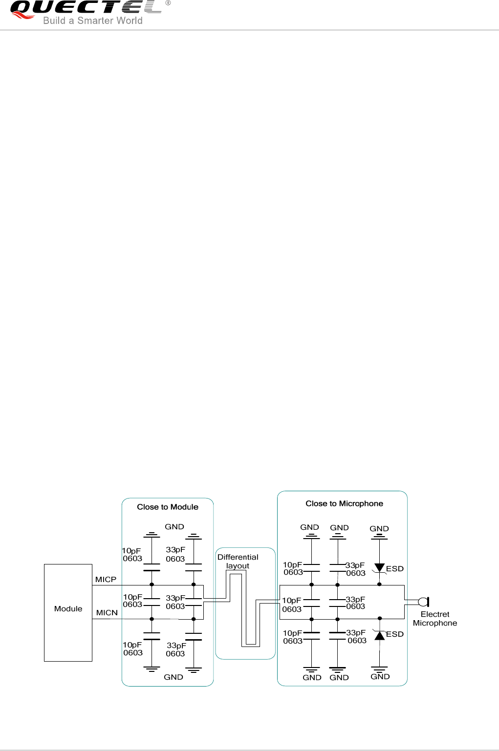
GSM/GPRS/GNSS Module Series
MC20 Hardware Design
MC20_Hardware_Design Confidential / Released 54 / 95
3.7.1. Decrease TDD Noise and Other Noises
The 33pF capacitor is applied for filtering out 900MHz RF interference when the module is transmitting at
EGSM900MHz. Without placing this capacitor, TDD noise could be heard. Moreover, the 10pF capacitor
here is used for filtering out 1800MHz RF interference. However, the resonant frequency point of a
capacitor largely depends on the material and production technique. Therefore, customers would have to
discuss with their capacitor vendors to choose the most suitable capacitor for filtering out GSM850MHz,
EGSM900MHz, DCS1800MHz and PCS1900MHz separately.
The severity degree of the RF interference in the voice channel during GSM transmitting period largely
depends on the application design. In some cases, EGSM900 TDD noise is more severe; while in other
cases, DCS1800 TDD noise is more obvious. Therefore, you can have a choice based on test results.
Sometimes, even no RF filtering capacitor is required.
The capacitor which is used for filtering out RF noise should be close to the audio interface. Audio
alignment should be as short as possible.
In order to decrease radio or other signal interference, the position of RF antenna should be kept away
from audio interface and audio alignment. Power alignment and audio alignment should not be parallel,
and power alignment should be far away from audio alignment.
The differential audio traces must be routed according to the differential signal layout rule.
3.7.2. Microphone Interfaces Design
AIN channels come with internal bias supply for external electret microphone. A reference circuit is shown
in the following figure.
Figure 25: Reference Design for AIN
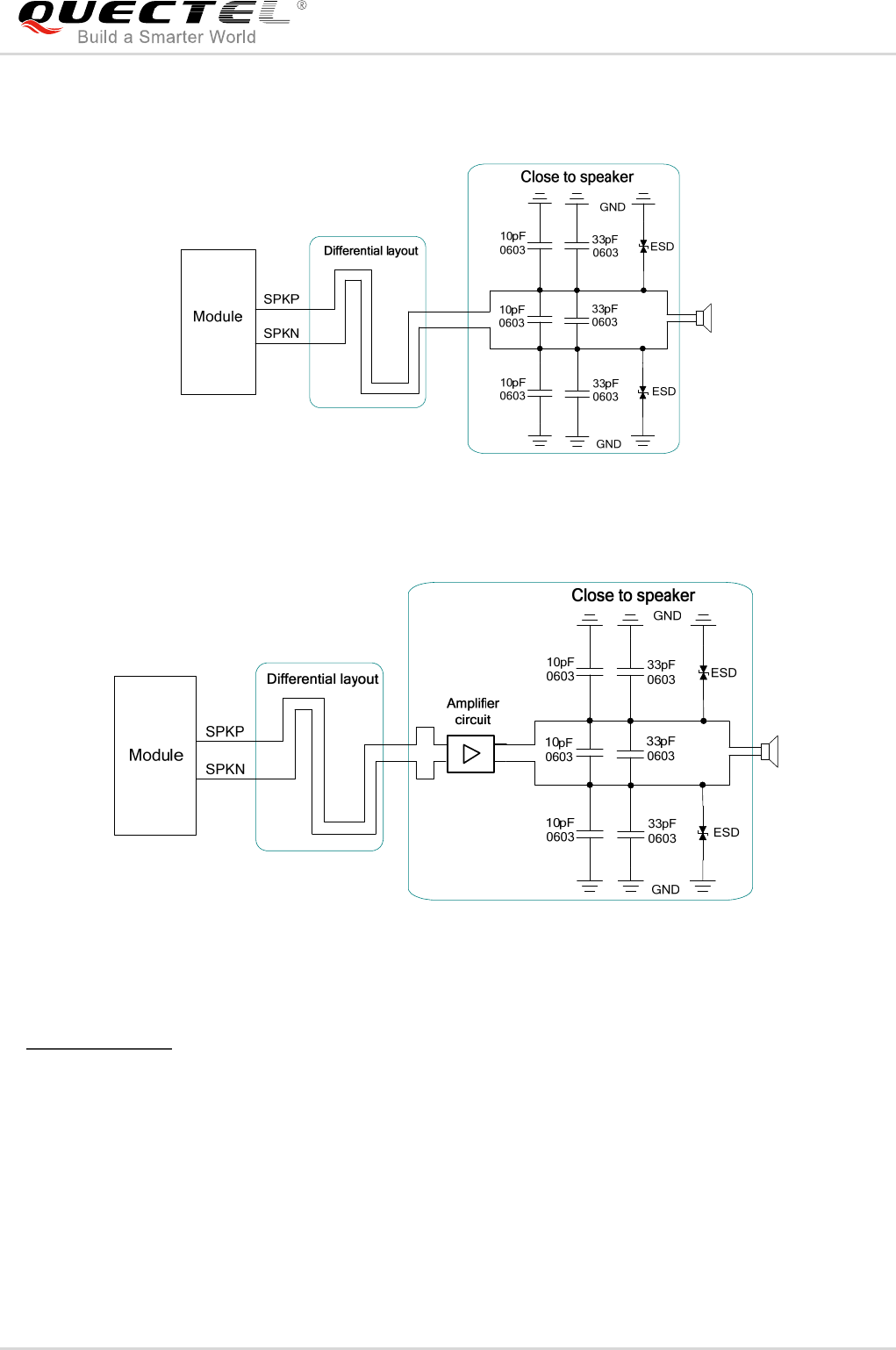
GSM/GPRS/GNSS Module Series
MC20 Hardware Design
MC20_Hardware_Design Confidential / Released 55 / 95
3.7.3. Receiver and Speaker Interface Design
Figure 26: Handset Interface Design for AOUT1
Figure 27: Speaker Interface Design with an Amplifier for AOUT1
A suitable differential audio amplifier can be chosen from the Texas Instrument’s website
(http://www.ti.com/). There are also other excellent audio amplifier vendors in the market.
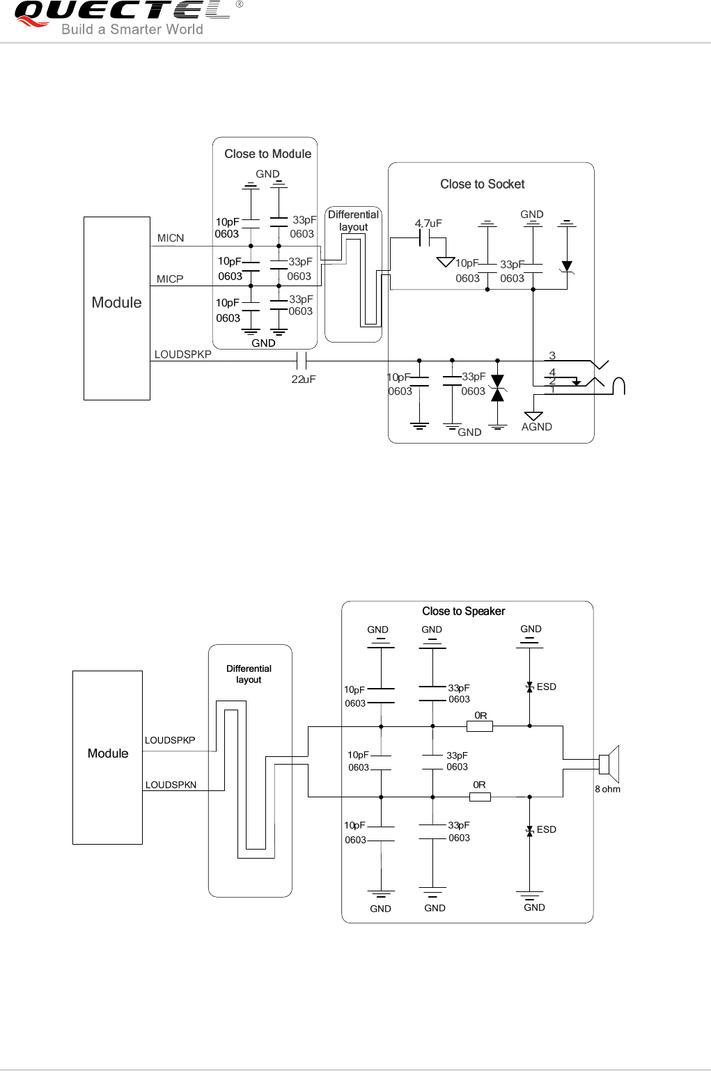
GSM/GPRS/GNSS Module Series
MC20 Hardware Design
MC20_Hardware_Design Confidential / Released 56 / 95
3.7.4. Earphone Interface Design
Figure 28: Earphone Interface Design
3.7.5. Loud Speaker Interface Design
Figure 29: Loud Speaker Interface Design

GSM/GPRS/GNSS Module Series
MC20 Hardware Design
MC20_Hardware_Design Confidential / Released 57 / 95
3.7.6. Audio Characteristics
Table 17: Typical Electret Microphone Characteristics
Table 18: Typical Speaker Characteristics
3.8. SIM Card Interface
The SIM interface supports the functionality of the GSM Phase 1 specification and also the functionality of
the new GSM Phase 2+ specification for FAST 64 kbps SIM card (intended for use with a SIM application
tool-kit.
The SIM interface is powered by an internal regulator in the module. Both 1.8V and 3.0V SIM cards are
supported, and Dual SIM Single Standby function is supported.
Parameter Min. Typ. Max. Unit
Working Voltage 1.2 1.5 2.0 V
Working Current 200 500 uA
External Microphone Load Resistance 2.2 K Ohm
Parameter Min. Typ. Max. Unit
AOUT1
Output
Single-ended
Load resistance 32 Ohm
Reference level 0 2.4 Vpp
Differential
Load resistance 32 Ohm
Reference level 0 4.8 Vpp
AOUT2
Output
Differential
Load resistance 8 Ohm
Reference level 0 2×VBAT Vpp
Single-ended
Load resistance 8 Ohm
Reference level 0 VBAT Vpp
GSM/GPRS/GNSS Module Series
MC20 Hardware Design
MC20_Hardware_Design Confidential / Released 58 / 95
Table 19: Pin Definition of the SIM Interface
1) If several interfaces share the same I/O pin, to avoid conflict between these alternate functions, only one
peripheral should be enabled at a time.
The following figure is a reference design for SIM1 interface with an 8-pin SIM card holder.
Pin Name Pin No. Description Alternate
Function1)
SIM1_VDD 18
Supply power for SIM card. Automatic detection of
SIM1 card voltage. 3.0V±5% and 1.8V±5%.
Maximum supply current is around 10mA.
SIM1_CLK 19 SIM1 card clock.
SIM1_DATA 21 SIM1 card data I/O.
SIM1_RST 20 SIM1 card reset.
SIM1_PRESENCE 37 SIM1 card detection. DTR
SIM_GND 16 SIM card ground.
SIM2_VDD 13
Supply power for SIM card. Automatic detection of
SIM2 card voltage. 3.0V±5% and 1.8V±5%.
Maximum supply current is around 10mA.
SIM2_CLK 10 SIM2 card clock.
SIM2_DATA 11 SIM2 card data I/O.
SIM2_RST 12 SIM2 card reset.
NOTE
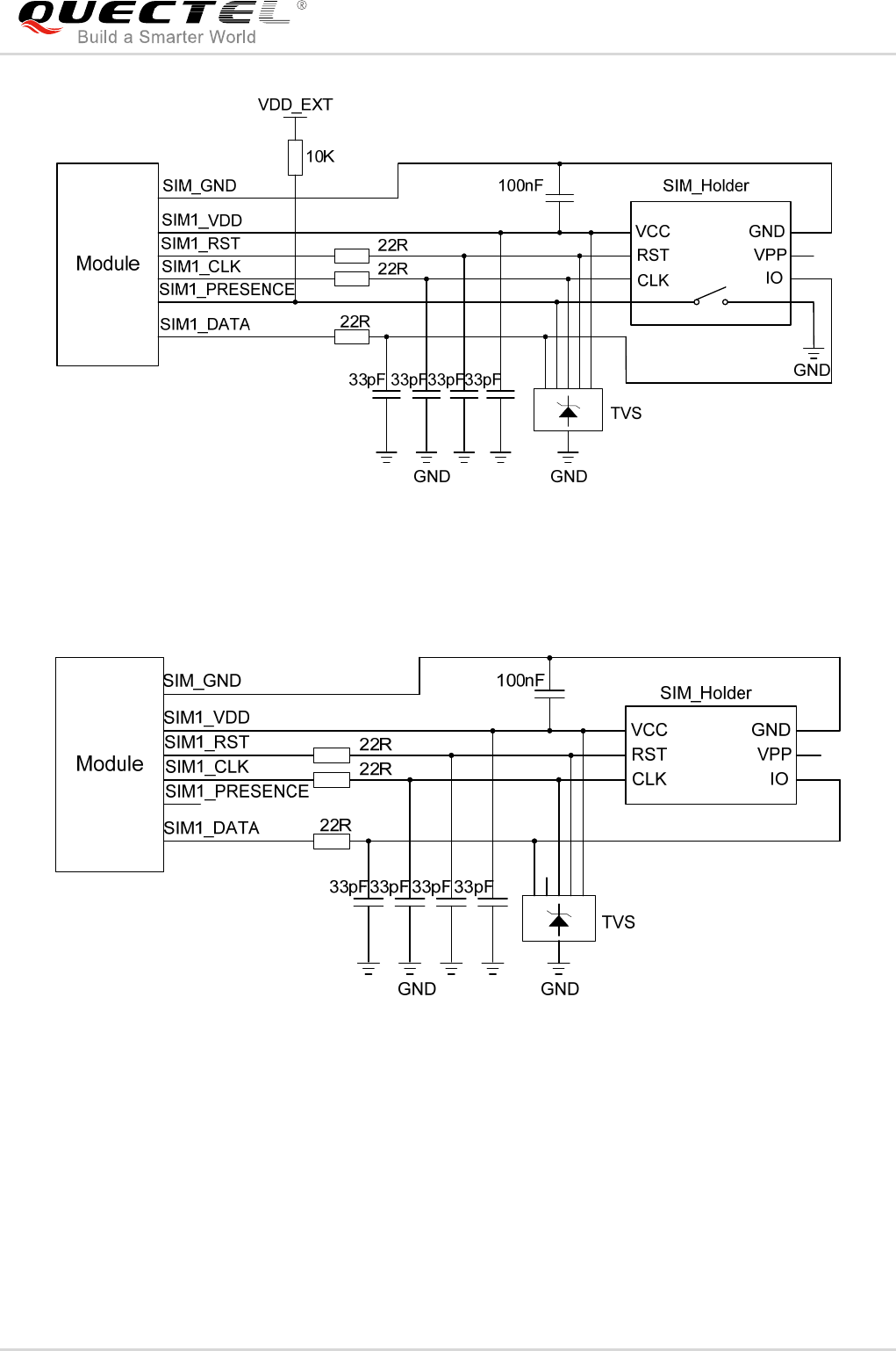
GSM/GPRS/GNSS Module Series
MC20 Hardware Design
MC20_Hardware_Design Confidential / Released 59 / 95
Figure 30: Reference Circuit for SIM1 Interface with an 8-pin SIM Card Holder
If SIM1 card detection function is not used, keep SIM1_PRESENCE pin open. A reference circuit for a
6-pin SIM card socket is shown in the following figure.
Figure 31: Reference Circuit for SIM1 Interface with a 6-pin SIM Card Holder
The following figure is a reference design for SIM2 interface with a 6-pin SIM card holder.
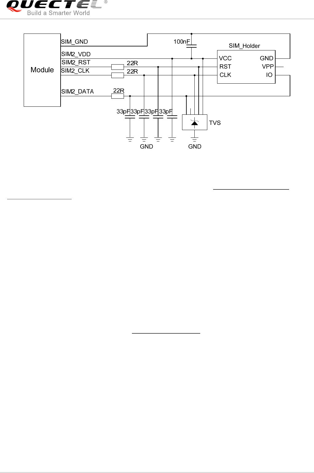
GSM/GPRS/GNSS Module Series
MC20 Hardware Design
MC20_Hardware_Design Confidential / Released 60 / 95
Figure 32: Reference Circuit for SIM2 Interface with a 6-pin SIM Card Holder
For more information of SIM card holder, you can visit http://www.amphenol.com/ and
http://www.molex.com/.
In order to enhance the reliability and availability of the SIM card in application, please conform to the
following criteria in the SIM circuit design:
Keep layout of SIM card as close to the module as possible. Assure the trace length is less than
200mm.
Keep SIM card signal away from RF and VBAT alignment.
Assure the ground between module and SIM holder short and wide. Keep the width of ground no less
than 0.5mm to maintain the same electric potential. The decouple capacitor of SIM_VDD is less than
1uF and must be near to SIM holder.
To avoid cross talk between SIM_DATA and SIM_CLK, keep them away from each other and shield
them with surrounded ground.
In order to offer good ESD protection, it is recommended to add a TVS diode array. For more
information of TVS diode, please visit http://www.onsemi.com/. The most important rule is to place
the ESD protection device close to the SIM card socket and make sure the nets being protected will
go through the ESD device first and then lead to module. The 22Ω resistors should be connected in
series between the module and the SIM card so as to suppress the EMI spurious transmission and
enhance the ESD protection. Please note that the SIM peripheral circuit should be close to the SIM
card socket.
Place the RF bypass capacitors (33pF) close to the SIM card on all signals lines to improve EMI
suppression performance.

GSM/GPRS/GNSS Module Series
MC20 Hardware Design
MC20_Hardware_Design Confidential / Released 61 / 95
3.9. ADC
The module provides an ADC channel to measure the value of voltage. Please give priority to the use of
ADC0 channel. Command AT+QADC can read the voltage value applied on ADC0 pin. For details of this
AT command, please refer to document [1]. In order to improve the accuracy of ADC, the layout of ADC
should be surrounded by ground.
Table 20: Pin Definition of the ADC
Table 21: Characteristics of the ADC
3.10. Behaviors of the RI
Table 22: Behaviors of the RI
Pin Name Pin No. Description
ADC 6 Analog to digital converter.
Item Min. Typ. Max. Unit
Voltage Range 0 2.8 V
ADC Resolution 10 bits
ADC Accuracy 2.7 mV
State RI Response
Standby HIGH
Voice Call
Change to LOW, and then:
1. Change to HIGH when call is established.
2. Change to HIGH when use ATH to hang up the call
3. Change to HIGH first when calling part hangs up and then change to LOW for
120ms indicating “NO CARRIER” as an URC. After that, RI changes to HIGH
again.
4. Change to HIGH when SMS is received.
SMS When a new SMS comes, the RI changes to LOW and holds low level for about
120ms, and then changes to HIGH.
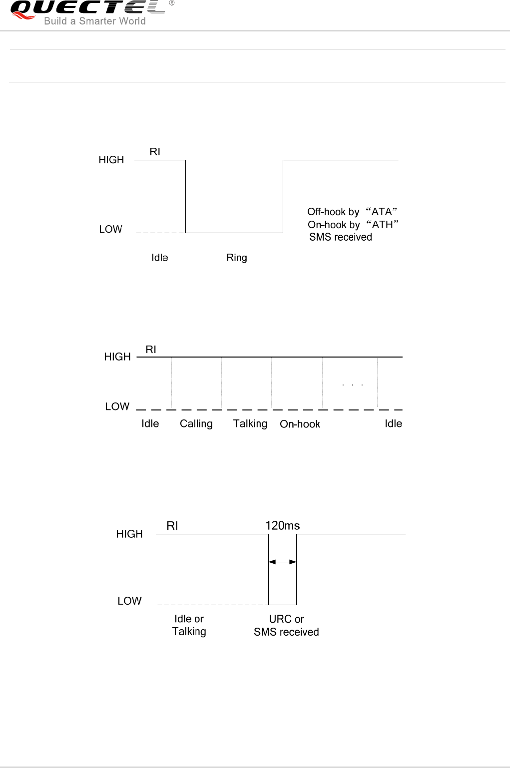
GSM/GPRS/GNSS Module Series
MC20 Hardware Design
MC20_Hardware_Design Confidential / Released 62 / 95
If the module is used as a caller, the RI would maintain high except when the URC or SMS is received.
When it is used as a receiver, the timing of RI is shown below.
Figure 33: RI Behavior as a Receiver When Voice Calling
Figure 34: RI Behavior as a Caller
Figure 35: RI Behavior When URC or SMS Received
URC Certain URCs can trigger 120ms low level on RI. For more details, please refer to
document [1]
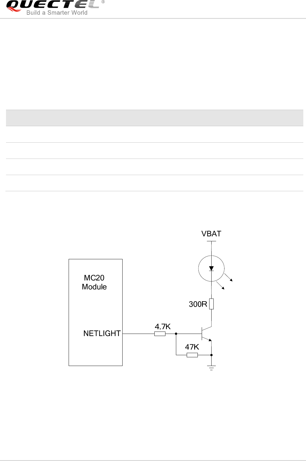
GSM/GPRS/GNSS Module Series
MC20 Hardware Design
MC20_Hardware_Design Confidential / Released 63 / 95
3.11. Network Status Indication
The NETLIGHT signal can be used to drive a network status indicator LED. The working state of this pin
is listed in the following table.
Table 23: Working State of the NETLIGHT
A reference circuit is shown as below.
Figure 36: Reference Design for NETLIGHT
State Module Function
Off The module is not running.
64ms On/800ms Off The module is not synchronized with network.
64ms On/2000ms Off The module is synchronized with network.
64ms On/600ms Off GPRS data transmission after dialing the PPP connection.
GSM/GPRS/GNSS Module Series
MC20 Hardware Design
MC20_Hardware_Design Confidential / Released 64 / 95
3.12. EASY Autonomous AGPS Technology
Supplying aiding information like ephemeris, almanac, rough last position, time and satellite status, can
help improve the acquisition sensitivity and the TTFF for a module. This is called as EASY technology and
MC20’s GNSS part supports it.
EASY technology works as embedded software which can accelerate TTFF by predicting satellite
navigation messages from received ephemeris. The GNSS part will calculate and predict orbit information
automatically up to 3 days after first receiving the broadcast ephemeris, and save the predicted
information into the internal memory. GNSS part of MC20 will use the information for positioning if no
enough information from satellites, so the function is helpful for positioning and TTFF improvement.
The EASY function can reduce TTFF to 5s in warm start. In this case, GNSS’s backup domain should be
valid. In order to gain enough broadcast ephemeris information from GNSS satellites, the GNSS part
should receive the information for at least 5 minutes in good signal conditions after it fixes the position.
EASY function is enabled by default. Command “$PMTK869,1,0*34” can be used to disable EASY
function. For more details, please refer to document [2].
3.13. EPO Offline AGPS Technology
MC20 module features a function called EPO (Extended Prediction Orbit) which is a world leading
technology. When MC20 module is powered on, EPO function can be enabled via AT command
AT+QGNSSEPO=1. When the GSM part detected that the EPO data has expired, the EPO data will be
automatically downloaded to the GSM part’s FS from MTK server via GSM/GPRS network; and the GNSS
part will get the EPO data via build-in GNSS command from GSM's FS when it detected that the local
EPO data has expired. When there is no local EPO data or when the data has expired, MC20 module will
download the data (4KB) for 6 hours’ orbit predictions in order to achieve cold start in the shortest time,
and then continue to download the EPO data (48KB) for 3 days. The technology allows the module to
realize fast positioning. Command AT+QGNSSEPO=0 can turn off the EPO function.
In all-in-one solution, make sure the GNSS part is powered on before sending the PMTK command.
Make sure the EPO function is enabled if you need to download the EPO data.
NOTE
NOTE
GSM/GPRS/GNSS Module Series
MC20 Hardware Design
MC20_Hardware_Design Confidential / Released 65 / 95
3.14. Multi-tone AIC
MC20 module has a function called multi-tone AIC (Active Interference Cancellation) to decease
harmonic of RF noise from Wi-Fi, GSM, 3G and 4G.
Up to 12 multi-tone AIC embedded in the module can provide effective narrow-band interference and
jamming elimination. The GNSS signal could be demodulated from the jammed signal, which can ensure
better navigation quality. AIC function is enabled by default. Enabling AIC function will increase current
consumption by about 1mA @VCC=3.3V. The following commands can be used to set AIC function.
Enable AIC function: $PMTK 286,1*23
Disable AIC function: $PMTK 286,0*22
In all-in-one solution, make sure the GNSS part is powered on before sending these PMTK commands.
NOTE
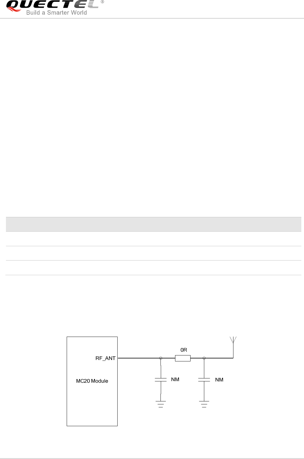
GSM/GPRS/GNSS Module Series
MC20 Hardware Design
MC20_Hardware_Design Confidential / Released 66 / 95
4 Antenna Interface
MC20 has three antenna interfaces which are used for GSM antenna, GNSS antenna and BT antenna,
respectively. The Pin 41 is the GSM antenna pad; the Pin 15 is the GNSS antenna pad; and Pin 32 is the
BT antenna pad. The RF interface of the three antenna pads has an impedance of 50Ω.
4.1. GSM Antenna Interface
There is a GSM antenna pad named RF_ANT for MC20.
Table 24: Pin Definition of the RF_ANT
4.1.1. Reference Design
The external antenna must be matched properly to achieve the best performance; so the matching circuit
is necessary. A reference design for GSM antenna is shown below.
Figure 37: Reference Design for GSM Antenna
Pin Name Pin No. Description
GND 40 Ground
RF_ANT 41 GSM antenna pad
GND 42 Ground

GSM/GPRS/GNSS Module Series
MC20 Hardware Design
MC20_Hardware_Design Confidential / Released 67 / 95
MC20 provides an RF antenna pad for antenna connection. The RF trace in host PCB connected to the
module’s RF antenna pad should be coplanar waveguide line or microstrip line, whose characteristic
impedance should be close to 50Ω. MC20 comes with grounding pads which are next to the antenna pad
in order to give a better grounding. Besides, a π type matching circuit is suggested to be used to adjust
the RF performance.
To minimize the loss on RF trace and RF cable, please pay attention to the design. The following table
shows the requirement on GSM antenna.
Table 25: Antenna Cable Requirements
Type Requirements
GSM850/EGSM900 Cable insertion loss <1dB
DCS1800/PCS1900 Cable insertion loss <1.5dB
Table 26: Antenna Requirements
Type Requirements
Frequency Range Depend on the frequency band(s) provided by the network operator
VSWR ≤ 2
Gain (dBi) 1
Max. Input Power (W) 50
Input Impedance (Ω) 50
Polarization Type Vertical
4.1.2. RF Output Power
Table 27: RF Output Power
Frequency Max. Min.
GSM850 33dBm±2dB 5dBm±5dB
EGSM900 33dBm±2dB 5dBm±5dB
DCS1800 30dBm±2dB 0dBm±5dB
GSM/GPRS/GNSS Module Series
MC20 Hardware Design
MC20_Hardware_Design Confidential / Released 68 / 95
In GPRS 4 slots TX mode, the maximum output power is reduced by 2.5dB. This design conforms to the
GSM specification as described in section 13.16 of 3GPP TS 51.010-1.
4.1.3. RF Receiving Sensitivity
Table 28: RF Receiving Sensitivity
4.1.4. Operating Frequencies
Table 29: Operating Frequencies
4.1.5. RF Cable Soldering
Soldering the RF cable to RF pad of module correctly will reduce the loss on the path of RF, please refer
to the following example of RF soldering.
PCS1900 30dBm±2dB 0dBm±5dB
Frequency Receive Sensitivity
GSM850 < -110dBm
EGSM900 < -110dBm
DCS1800 < -110dBm
PCS1900 < -110dBm
Frequency Receive Transmit ARFCH
GSM850 869~894MHz 824~849MHz 128~251
EGSM900 925~960MHz 880~915MHz 0~124, 975~1023
DCS1800 1805~1880MHz 1710~1785MHz 512~885
PCS1900 1930~1990MHz 1850~1910MHz 512~810
NOTE
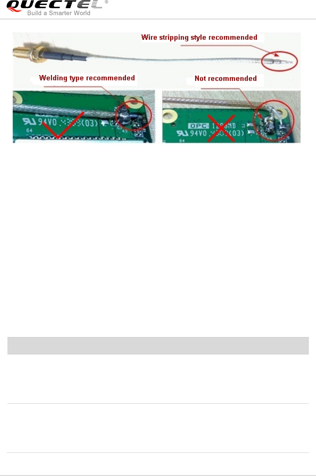
GSM/GPRS/GNSS Module Series
MC20 Hardware Design
MC20_Hardware_Design Confidential / Released 69 / 95
Figure 38: RF Soldering Sample
4.2. GNSS Antenna Interface
The GNSS part of MC20 module supports both GPS and BeiDou systems. The RF signal is obtained from
the GNSS_ANT pin. The impedance of RF trace should be controlled as 50 Ohm, and the trace length
should be kept as short as possible.
4.2.1. Antenna Specifications
The module can be connected to a dedicated GPS/BeiDou passive or active antenna to receive
GPS/BeiDou satellite signals. The recommended antenna specifications are given in the following table.
Table 30: Recommended Antenna Specifications
Antenna Type Specification
Passive Antenna
GPS frequency: 1575.42±2MHz
BeiDou frequency: 1602±4MHz
VSWR: <2 (Typ.)
Polarization: RHCP or Linear
Gain: >0dBi
Active Antenna
GPS frequency: 1575.42±2MHz
BeiDou frequency:1602±4MHz
VSWR: <2 (Typ.)
Polarization: RHCP or Linear
Noise figure: <1.5dB
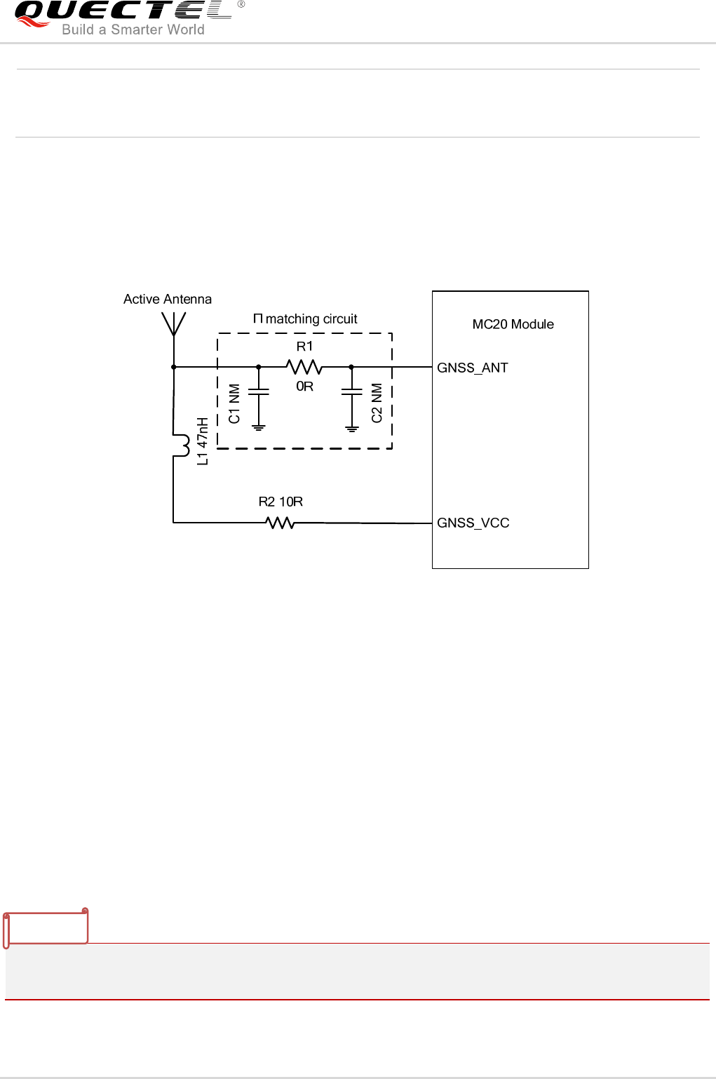
GSM/GPRS/GNSS Module Series
MC20 Hardware Design
MC20_Hardware_Design Confidential / Released 70 / 95
4.2.2. Active Antenna
The following figure is a typical reference design with active antenna. In this mode, the antenna is
powered by GNSS_VCC.
Figure 39: Reference Design with Active Antenna
C1, R1 and C2 are reserved matching circuit for antenna impedance modification. By default, C1 and C2
are not mounted; R1 is 0 ohm.
The external active antenna is powered by GNSS_VCC. The voltage ranges from 2.8V to 4.3V, and the
typical value is 3.3V. If the voltage does not meet the requirements for powering the active antenna, an
external LDO should be used.
The inductor L1 is used to prevent the RF signal from leaking into the GNSS_VCC pin and route the bias
supply to the active antenna, and the recommended value of L1 is no less than 47nH. R2 can protect the
whole circuit in case the active antenna is shorted to ground.
In all-in-one solution, please note that the power supply of GNSS_VCC is controlled by the GSM part
through AT command.
Gain (antenna): >-2dBi
Gain (embedded LNA): 20dB (Typ.)
Total gain: >18dBi (Typ.)
NOTE
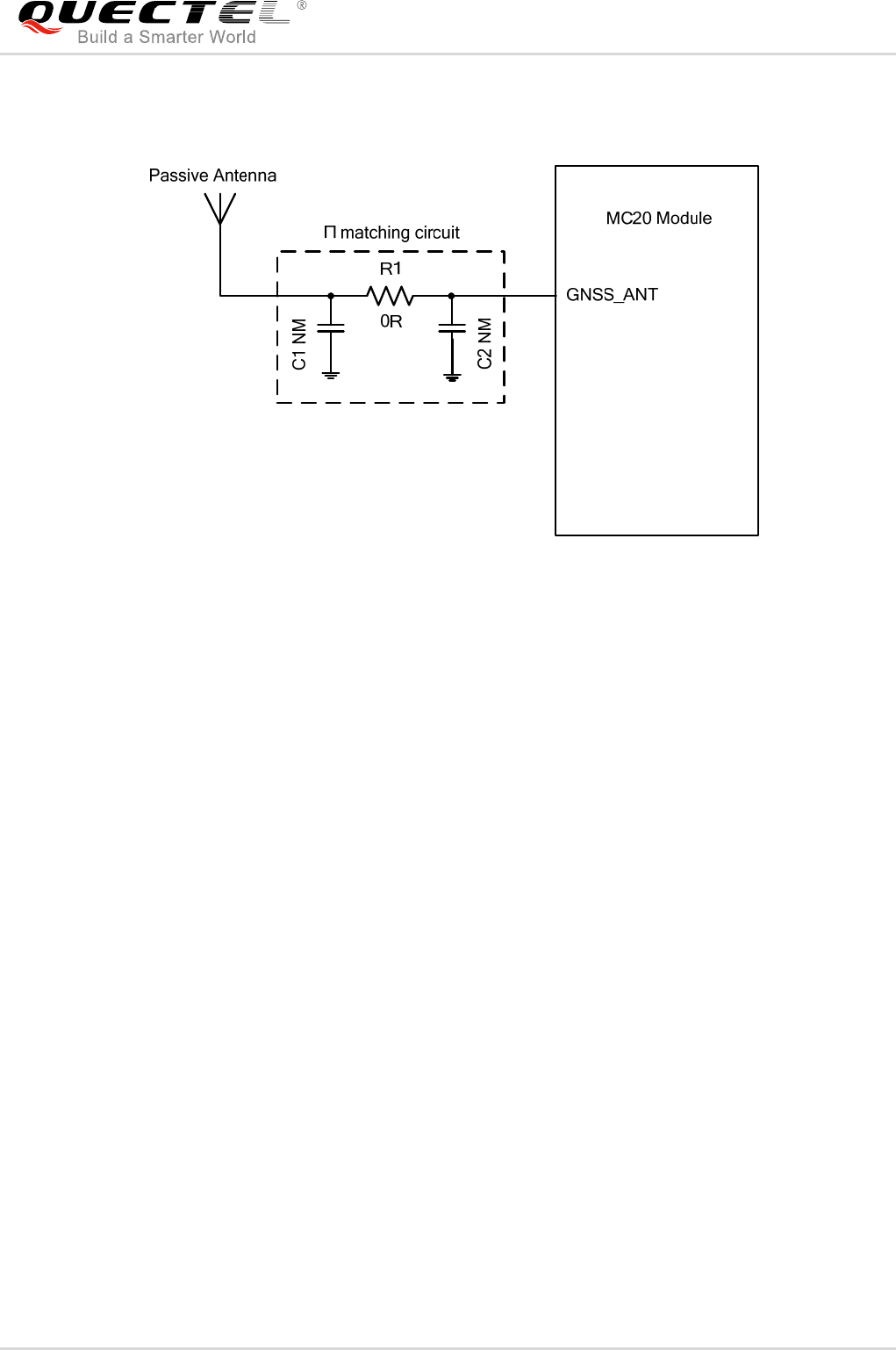
GSM/GPRS/GNSS Module Series
MC20 Hardware Design
MC20_Hardware_Design Confidential / Released 71 / 95
4.2.3. Passive Antenna
Figure 40: Reference Design with Passive Antenna
The above figure is a typical reference design with passive antenna.
C1, R1 and C2 are reserved matching circuit for antenna impedance modification. C1 and C2 are not
mounted by default; R1 is 0 ohm. Impedance of RF trace should be controlled as 50 ohm and the trace
length should be kept as short as possible.
4.3. Bluetooth Antenna Interface
MC20 provides a Bluetooth antenna interface. Bluetooth is a wireless technology that allows devices to
communicate, or transmit data/voice, wirelessly over a short distance. It is described as a short-range
communication technology intended to replace the cables connecting portable and/or fixed devices while
maintaining high level of security. Bluetooth is standardized as IEEE802.15 and operates in the 2.4 GHz
range using RF technology. Its data rate is up to 3Mbps.
MC20 is fully compliant with Bluetooth specification 3.0, and supports profiles including SPP and HFP-AG.
The module provides a Bluetooth antenna pad named BT_ANT, and the pin definition is listed below.
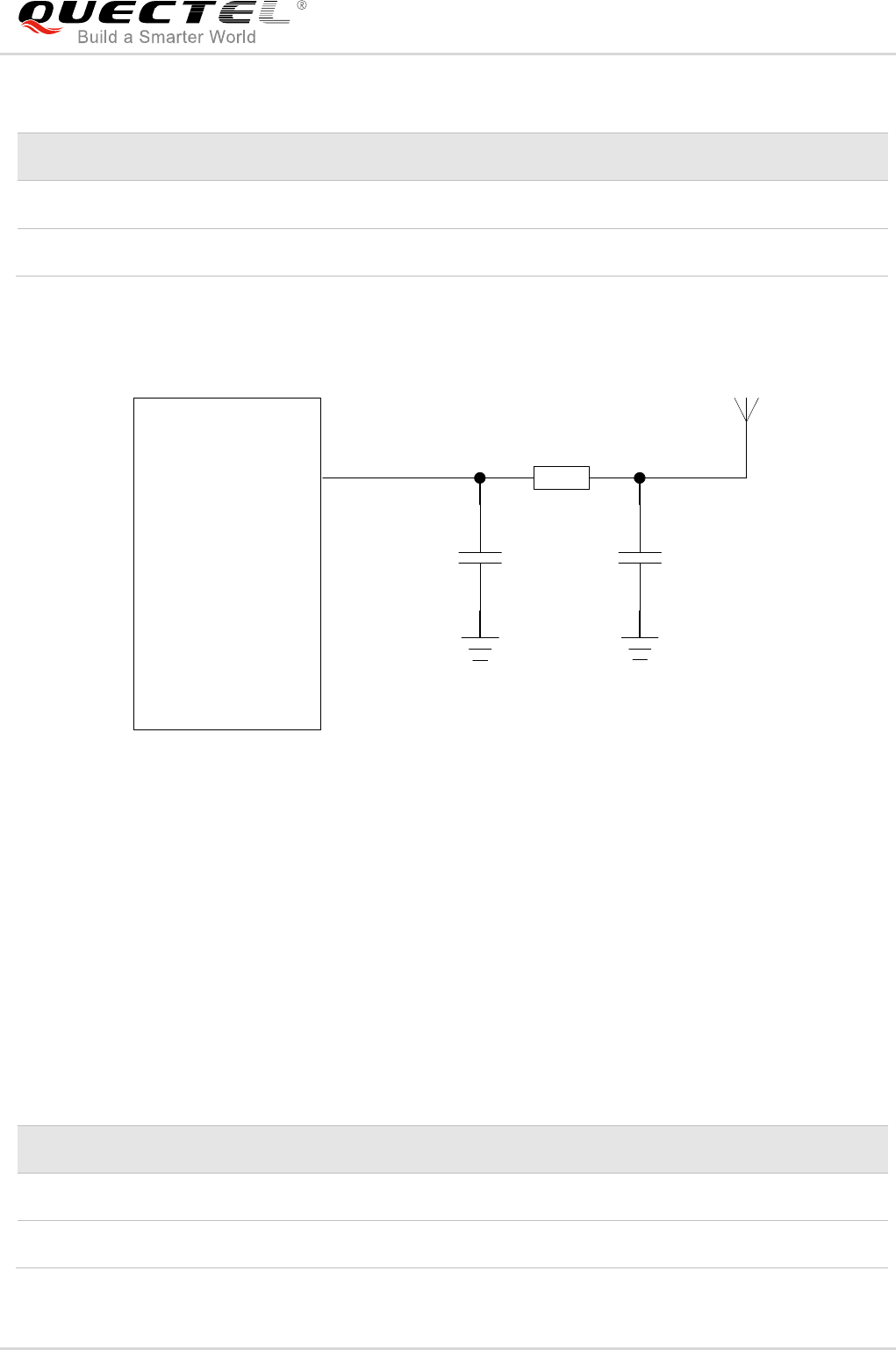
GSM/GPRS/GNSS Module Series
MC20 Hardware Design
MC20_Hardware_Design Confidential / Released 72 / 95
Table 31: Pin Definition of the BT_ANT
The external antenna must be matched properly to achieve the best performance, so the matching circuit
is necessary. The connection is recommended as in the following figure:
MC20 Module
BT_ANT
0R
NM NM
Figure 41: Reference Design for Bluetooth Antenna
There are some suggestions for component placement and RF trace layout for Bluetooth RF traces:
Antenna matching circuit should be closed to the antenna;
The impedance of RF trace should be controlled as 50Ω;
The RF traces should be kept far away from the high frequency signals and strong disturbing source.
The proposed antenna type is Chip antenna,and the detailed description is as follows:
Table 32: Recommended Antenna Specifications
Pin Name Pin No. Description
BT_ANT 32 BT antenna pad
GND 31 Ground
ITEM SPECIFICATION
Type Chip Antenna
Frequency Band 2.40GHz~2.50GHz

GSM/GPRS/GNSS Module Series
MC20 Hardware Design
MC20_Hardware_Design Confidential / Released 73 / 95
Peak Gain 3 dBi Typ
Impedance 50Ω Typ

GSM/GPRS/GNSS Module Series
MC20 Hardware Design
MC20_Hardware_Design Confidential / Released 74 / 95
5 Electrical, Reliability and Radio
Characteristics
5.1. Absolute Maximum Ratings
Absolute maximum ratings for power supply and voltage on digital and analog pins of the module are
listed in the following table:
Table 33: Absolute Maximum Ratings
5.2. Operating Temperature
The operating temperature is listed in the following table:
Parameter Min. Max. Unit
VBAT -0.3 +4.73 V
GNSS_VCC -0.3 +4.5 V
Peak Current of Power Supply (VBAT) 0 2 A
RMS Current of Power Supply (VBAT, during one
TDMA-frame) 0 0.7 A
Voltage at Digital Pins -0.3 3.08 V
Voltage at Analog Pins -0.3 3.08 V
Voltage at Digital/analog Pins in Power Down Mode -0.25 0.25 V
GSM/GPRS/GNSS Module Series
MC20 Hardware Design
MC20_Hardware_Design Confidential / Released 75 / 95
Table 34: Operating Temperature
1. 1) Within operation temperature range, the module is 3GPP compliant.
2. 2) Within extended temperature range, the module remains the ability to establish and maintain a
voice, SMS, data transmission, emergency call, etc. There is no unrecoverable malfunction. There
are also no effects on radio spectrum and no harm to radio network. Only one or more parameters like
Pout might reduce in their value and exceed the specified tolerances. When the temperature returns to
the normal operating temperature levels, the module will meet 3GPP compliant again.
5.3. Power Supply Ratings
Table 35: Power Supply Ratings of GSM Part (GNSS is Powered off)
Parameter Min. Typ. Max. Unit
Operation temperature range 1) -35 +25 +75 ℃
Extended temperature range 2) -40 +85 ℃
Parameter Description Conditions Min. Typ. Max. Unit
VBAT
Supply voltage
Voltage must stay within the
min/max values, including
voltage drop, ripple, and spikes.
3.3 4.0 4.6 V
Voltage drop
during
transmitting
burst
Maximum power control level
on GSM850 and EGSM900. 400 mV
IVBAT Average supply
current
Power down mode
SLEEP mode @DRX=5
220
1.2
uA
mA
Minimum functionality mode
AT+CFUN=0
IDLE mode
SLEEP mode
AT+CFUN=4
IDLE mode
SLEEP mode
13
0.68
13
0.73
mA
mA
mA
mA
TALK mode
GSM850/EGSM9001)
DCS1800/PCS19002)
208/209
142/146
mA
mA
NOTES
GSM/GPRS/GNSS Module Series
MC20 Hardware Design
MC20_Hardware_Design Confidential / Released 76 / 95
1. 1) Power control level PCL 5.
2. 2) Power control level PCL 0.
3. 3) Under the GSM850 and EGSM900 spectrum, the power of 1Rx and 4Tx is reduced.
Table 36: Power Supply Ratings of GNSS Part
Parameter Description Conditions Min. Typ. Max. Unit
GNSS_
VCC Supply voltage
Voltage must stay
within the min/max
values, including
voltage drop, ripple,
and spikes.
2.8 3.3 4.3 V
IVCCP1) Peak supply current VCC=3.3V 150 mA
1) This figure can be used to determine the maximum current capability of power supply.
DATA mode, GPRS (3Rx, 2Tx)
GSM850/EGSM9001)
DCS1800/PCS19002)
359/360
232/250
mA
mA
DATA mode, GPRS (2 Rx, 3Tx)
GSM850/EGSM9001)
DCS1800/PCS19002)
431/413
311/339
mA
mA
DATA mode, GPRS (4 Rx, 1Tx)
GSM850/EGSM9001)
DCS1800/PCS19002)
215/153
153/162
mA
mA
DATA mode, GPRS (1Rx, 4Tx)
GSM850/EGSM9001)
DCS1800/PCS19002)
499/4693)
392/427
mA
mA
Peak supply
current (during
transmission
slot)
Maximum power control level
on GSM850 and EGSM900. 1.6 2 A
NOTES
NOTE

GSM/GPRS/GNSS Module Series
MC20 Hardware Design
MC20_Hardware_Design Confidential / Released 77 / 95
5.4. Current Consumption
Table 37: Current Consumption of GSM Part (GNSS is Powered off)
Condition Current Consumption
Voice Call
GSM850
@power level #5 <300mA, Typical 174mA
@power level #12, Typical 83mA
@power level #19, Typical 62mA
EGSM900
@power level #5 <300mA, Typical 175mA
@power level #12, Typical 83mA
@power level #19, Typical 63mA
DCS1800
@power level #0 <250mA, Typical 153mA
@power level #7, Typical 73mA
@power level #15, Typical 60mA
PCS1900
@power level #0 <250mA, Typical 151mA
@power level #7, Typical 76mA
@power level #15, Typical 61mA
GPRS Data
DATA Mode, GPRS (3 Rx, 2Tx) CLASS 12
GSM850
@power level #5 <550mA, Typical 363mA
@power level #12, Typical 131mA
@power level #19, Typical 91mA
EGSM900
@power level #5 <550mA, Typical 356mA
@power level #12, Typical 132mA
@power level #19, Typical 92mA
DCS1800
@power level #0 <450mA, Typical 234mA
@power level #7, Typical 112mA
@power level #15, Typical 88mA
PCS1900
@power level #0 <450mA, Typical 257mA
@power level #7, Typical 119mA
@power level #15, Typical 89mA
DATA Mode, GPRS (2 Rx, 3Tx) CLASS 12
GSM850
@power level #5 <640mA, Typical 496mA
@power level #12, Typical 159mA
@power level #19, Typical 99mA
EGSM900 @power level #5 <600mA, Typical 487mA
@power level #12, Typical 160mA
GSM/GPRS/GNSS Module Series
MC20 Hardware Design
MC20_Hardware_Design Confidential / Released 78 / 95
GPRS Class 12 is the default setting. The GSM module can be configured from GPRS Class 1 to Class
12. Setting to lower GPRS class would make it easier to design the power supply for the GSM module.
@power level #19, Typical 101mA
DCS1800
@power level #0 <490mA, Typical 305mA
@power level #7, Typical 131mA
@power level #15, Typical 93mA
PCS1900
@power level #0 <480mA, Typical 348mA
@power level #7, Typical 138mA
@power level #15, Typical 94mA
DATA Mode, GPRS (4 Rx,1Tx) CLASS 12
GSM850
@power level #5 <350mA, Typical 216mA
@power level #12, Typical 103mA
@power level #19, Typical 83mA
EGSM900
@power level #5 <350mA, Typical 222mA
@power level #12, Typical 104mA
@power level #19, Typical 84mA
DCS1800
@power level #0 <300mA, Typical 171mA
@power level #7, Typical 96mA
@power level #15, Typical 82mA
PCS1900
@power level #0 <300mA, Typical 169mA
@power level #7, Typical 98mA
@power level #15, Typical 83mA
DATA Mode, GPRS (1 Rx, 4Tx) CLASS 12
GSM850
@power level #5 <600mA, Typical 470mA
@power level #12, Typical 182mA
@power level #19, Typical 106mA
EGSM900
@power level #5 <600mA, Typical 471mA
@power level #12, Typical 187mA
@power level #19, Typical 109mA
DCS1800
@power level #0 <500mA, Typical 377mA
@power level #7, Typical 149mA
@power level #15, Typical 97mA
PCS1900
@power level #0 <500mA, Typical 439mA
@power level #7, Typical 159mA
@power level #15, Typical 99mA
NOTE
GSM/GPRS/GNSS Module Series
MC20 Hardware Design
MC20_Hardware_Design Confidential / Released 79 / 95
Table 38: Current Consumption of the GNSS Part
Parameter Conditions Typ. Unit
IVCC @Acquisition @VCC=3.3V (GPS) 25 mA
IVCC @Tracking @VCC=3.3V (GPS) 19 mA
IVCC @Acquisition @VCC=3.3V (GPS+BeiDou) 23 mA
IVCC @Tracking @VCC=3.3V (GPS+BeiDou) 18 mA
IVCC @Standby @VCC=3.3V 0.3 mA
IBCKP @backup @V_BCKP=3.3V 14 uA
The tracking current is tested in following conditions:
For Cold Start, 10 minutes after First Fix.
For Hot Start, 15 seconds after First Fix.
5.5. Electrostatic Discharge
Although the module is generally protected against Electrostatic Discharge (ESD), ESD protection
precautions should still be emphasized. Proper ESD handling and packaging procedures must be applied
throughout the processing, handling and operation of any applications using the module.
The measured ESD values of the module are shown in the following table.
Table 39: ESD Endurance (Temperature: 25ºC, Humidity: 45%)
Tested Point Contact Discharge Air Discharge
VBAT, GND ±5KV ±10KV
RF_ANT ±5KV ±10KV
TXD, RXD ±2KV ±4KV
GNSS_TXD
GNSS_RXD ±2KV ±4KV
Others ±0.5KV ±1KV
NOTE

GSM/GPRS/GNSS Module Series
MC20 Hardware Design
MC20_Hardware_Design Confidential / Released 80 / 95
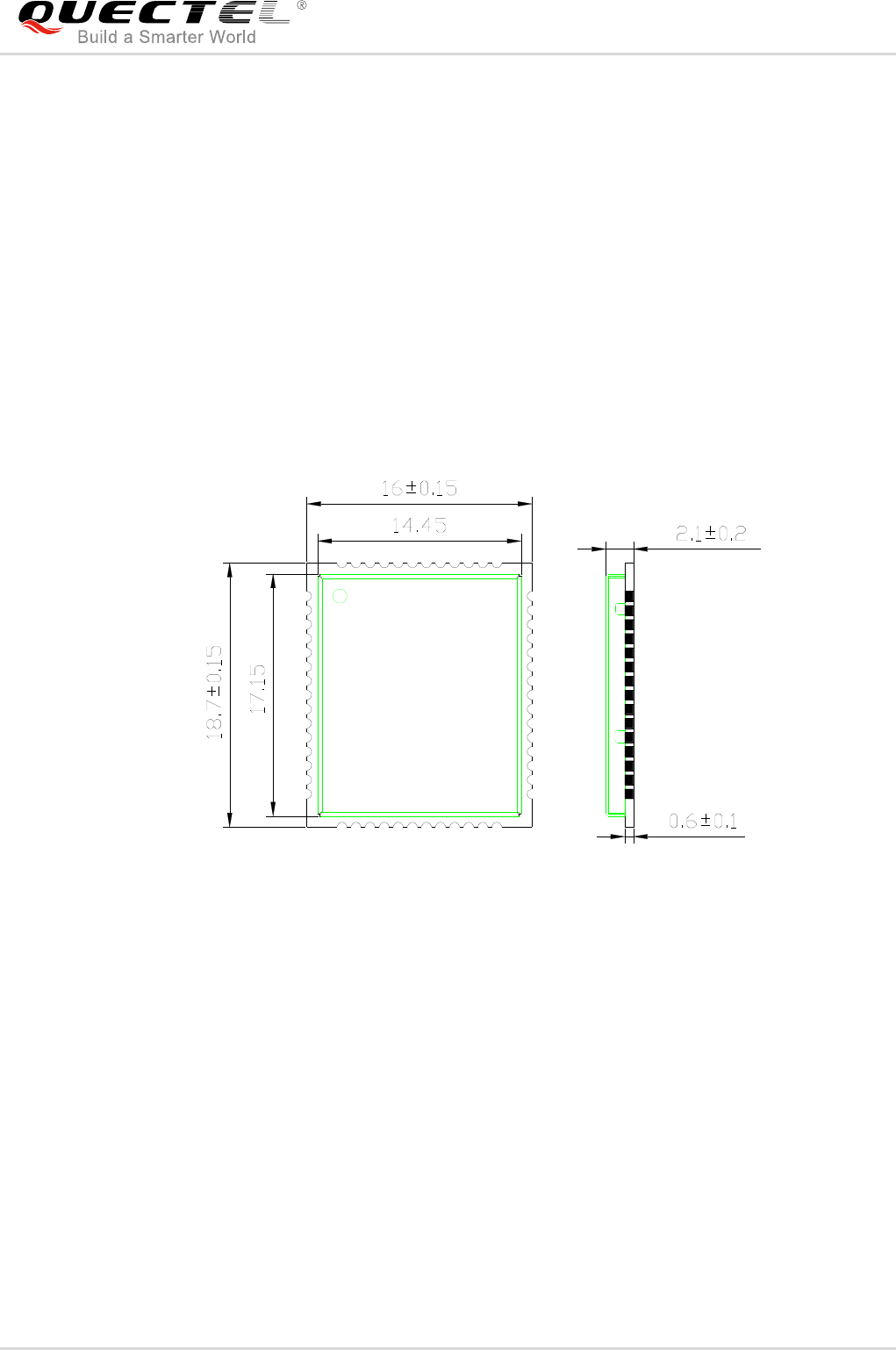
GSM/GPRS/GNSS Module Series
MC20 Hardware Design
MC20_Hardware_Design Confidential / Released 81 / 95
6 Mechanical Dimensions
This chapter describes the mechanical dimensions of the module.
6.1. Mechanical Dimensions of Module
Figure 42: MC20 Top and Side Dimensions (Unit: mm)
GSM/GPRS/GNSS Module Series
MC20 Hardware Design
MC20_Hardware_Design Confidential / Released 82 / 95
Figure 43: MC20 Bottom Dimensions (Unit: mm)
GSM/GPRS/GNSS Module Series
MC20 Hardware Design
MC20_Hardware_Design Confidential / Released 83 / 95
6.2. Recommended Footprint
Figure 44: Recommended Footprint (Unit: mm)
1. For convenient maintenance, the module should be kept about 3mm away from the other
components in the host PCB.
2. The circular test points with a radius of 1.75mm in the above recommended footprint should be
treated as keepout areas. (“keepout” means do not pour copper on the mother board).
NOTES
GSM/GPRS/GNSS Module Series
MC20 Hardware Design
MC20_Hardware_Design Confidential / Released 84 / 95
6.3. Top and Bottom View of the Module
Figure 45: Top View of the Module
Figure 46: Bottom View of the Module
These are design effect drawings of MC20 module. For more accurate pictures, please refer to the
module that you get from Quectel.
NOTE
GSM/GPRS/GNSS Module Series
MC20 Hardware Design
MC20_Hardware_Design Confidential / Released 85 / 95
7 Storage and Manufacturing
7.1. Storage
MC20 module is stored in a vacuum-sealed bag. The storage restrictions are shown as below.
1. Shelf life in the vacuum-sealed bag: 12 months at <40ºC and <90%RH.
2. After the vacuum-sealed bag is opened, devices that need to be mounted directly must be:
Mounted within 72 hours at the factory environment of ≤30ºC and <60% RH.
Stored at <10% RH.
3. Devices require baking before mounting, if any circumstance below occurs.
When the ambient temperature is 23ºC±5ºC and the humidity indication card shows the humidity
is >10% before opening the vacuum-sealed bag.
Device mounting cannot be finished within 72 hours when the ambient temperature is <30ºC and the
humidity is <60%.
Stored at >10% RH.
4. If baking is required, devices should be baked for 48 hours at 125ºC±5ºC.
As the plastic package cannot be subjected to high temperature, it should be removed from devices
before high temperature (125ºC) baking. If shorter baking time is desired, please refer to
IPC/JEDECJ-STD-033 for baking procedure.
7.2. Soldering
Push the squeegee to apply the solder paste on the surface of stencil, thus making the paste fill the
stencil openings and then penetrate to the PCB. The force on the squeegee should be adjusted properly
so as to produce a clean stencil surface on a single pass. To ensure the module soldering quality, the
NOTE
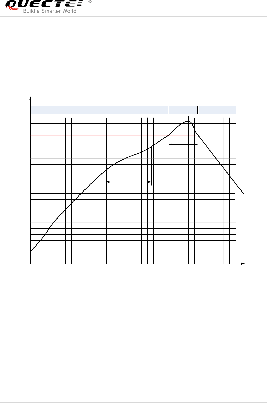
GSM/GPRS/GNSS Module Series
MC20 Hardware Design
MC20_Hardware_Design Confidential / Released 86 / 95
thickness of stencil at the hole of the module pads should be 0.2 mm for MC20. For more details, please
refer to document [12]
It is suggested that the peak reflow temperature is from 235ºC to 245ºC (for SnAg3.0Cu0.5 alloy). The
absolute maximum reflow temperature is 260ºC. To avoid damage to the module caused by repeated
heating, it is suggested that the module should be mounted after reflow soldering for the other side of
PCB has been completed. Recommended reflow soldering thermal profile is shown below:
Time(s)
50 100 150 200 250 300
50
100
150
200
250
160℃
200℃
217
0
70s~120s
40s~60s
Between 1~3℃/S
Preheat Heating Cooling
℃
s
Liquids
Temperature
Figure 47: Reflow Soldering Thermal Profile
7.3. Packaging
The modules are stored in a vacuum-sealed bag which is ESD protected. It should not be opened until the
devices are ready to be soldered onto the application.
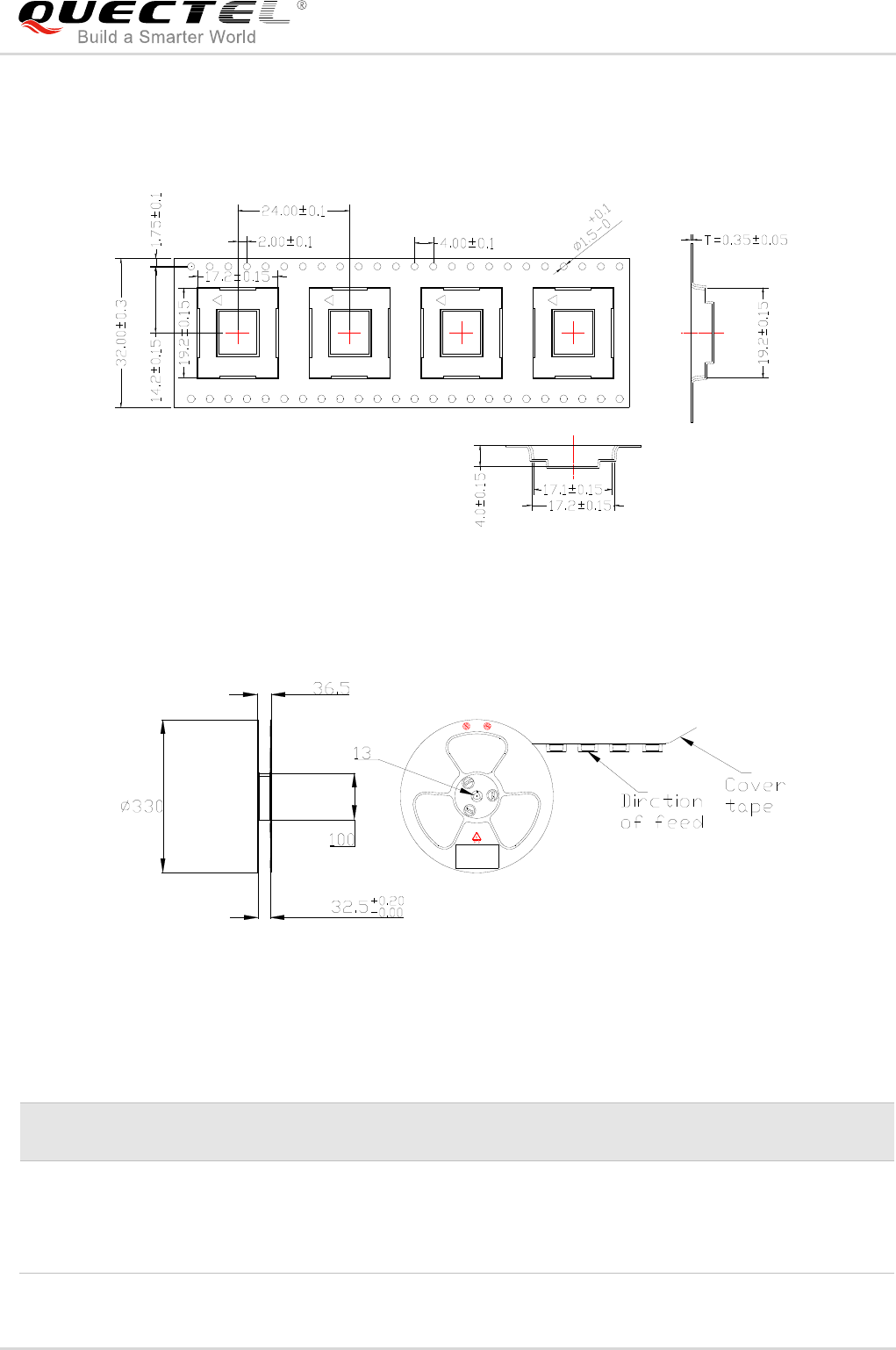
GSM/GPRS/GNSS Module Series
MC20 Hardware Design
MC20_Hardware_Design Confidential / Released 87 / 95
7.3.1. Tape and Reel Packaging
Figure 48: Tape and Reel Specification
Figure 49: Dimensions of Reel
Table 40: Reel Packaging
Model Name MOQ for
MP
Minimum
Package:250pcs
Minimum
Packagex4=1000pcs
MC20 250pcs
Size:
370mm×350mm×56mm
N.W: 0.32kg
G.W: 1.08kg
Size:
380mm×250mm×365mm
N.W: 1.28kg
G.W: 4.8kg

GSM/GPRS/GNSS Module Series
MC20 Hardware Design
MC20_Hardware_Design Confidential / Released 88 / 95
8 Appendix A References
Table 41: Related Documents
SN Document Name Remark
[1] Quectel_MC20_AT_Commands_Manual MC20 AT commands manual
[2] ITU-T Draft new recommendation V.25ter Serial asynchronous automatic dialing
and control
[3] GSM 07.07
Digital cellular telecommunications
(Phase 2+); AT command set for GSM
Mobile Equipment (ME)
[4] GSM 07.10 Support GSM 07.10 multiplexing
protocol
[5] GSM 07.05
Digital cellular telecommunications
(Phase 2+); Use of Data Terminal
Equipment – Data Circuit terminating
Equipment (DTE – DCE) interface for
Short Message Service (SMS) and
Cell Broadcast Service (CBS)
[6] GSM 11.14
Digital cellular telecommunications
(Phase 2+); Specification of the SIM
Application Toolkit for the Subscriber
Identity module – Mobile Equipment
(SIM – ME) interface
[7] GSM 11.11
Digital cellular telecommunications
(Phase 2+); Specification of the
Subscriber Identity module – Mobile
Equipment (SIM – ME) interface
[8] GSM 03.38
Digital cellular telecommunications
(Phase 2+); Alphabets and
language-specific information
[9] GSM 11.10
Digital cellular telecommunications
(Phase 2); Mobile Station (MS)
conformance specification; Part 1:
Conformance specification

GSM/GPRS/GNSS Module Series
MC20 Hardware Design
MC20_Hardware_Design Confidential / Released 89 / 95
Table 42: Terms and Abbreviations
[10] GSM_UART_Application_Note UART port application note
[11] GSM_EVB_User_Guide GSM EVB user guide
[12] Module_Secondary_SMT_User_Guide Module secondary SMT user guide
[13] Quectel_GSM_Module_Digital_IO_Application_Note GSM Module Digital IO Application
Note
Abbreviation Description
ADC Analog-to-Digital Converter
AMR Adaptive Multi-Rate
ARP Antenna Reference Point
ASIC Application Specific Integrated Circuit
BER Bit Error Rate
BOM Bill of Material
BT Bluetooth
BTS Base Transceiver Station
CHAP Challenge Handshake Authentication Protocol
CS Coding Scheme
CSD Circuit Switched Data
CTS Clear to Send
DAC Digital-to-Analog Converter
DRX Discontinuous Reception
DSP Digital Signal Processor
DCE Data Communications Equipment (typically module)
DTE Data Terminal Equipment (typically computer, external controller)
DTR Data Terminal Ready

GSM/GPRS/GNSS Module Series
MC20 Hardware Design
MC20_Hardware_Design Confidential / Released 90 / 95
DTX Discontinuous Transmission
EFR Enhanced Full Rate
EGSM Enhanced GSM
EMC Electromagnetic Compatibility
ESD Electrostatic Discharge
ETS European Telecommunication Standard
FCC Federal Communications Commission (U.S.)
FDMA Frequency Division Multiple Access
FR Full Rate
FS File System
GMSK Gaussian Minimum Shift Keying
GPRS General Packet Radio Service
GSM Global System for Mobile Communications
G.W Gross Weight
HR Half Rate
I/O Input/Output
IC Integrated Circuit
IMEI International Mobile Equipment Identity
IOmax Maximum Output Load Current
kbps Kilo Bits Per Second
LED Light Emitting Diode
Li-Ion Lithium-Ion
MO Mobile Originated
MOQ Minimum Order Quantity
MP Manufacture Product

GSM/GPRS/GNSS Module Series
MC20 Hardware Design
MC20_Hardware_Design Confidential / Released 91 / 95
MS Mobile Station (GSM engine)
MT Mobile Terminated
N.W Net Weight
PAP Password Authentication Protocol
PBCCH Packet Switched Broadcast Control Channel
PCB Printed Circuit Board
PDU Protocol Data Unit
PPP Point-to-Point Protocol
RF Radio Frequency
RMS Root Mean Square (value)
RTC Real Time Clock
RX Receive Direction
SIM Subscriber Identification Module
SMS Short Message Service
TDMA Time Division Multiple Access
TE Terminal Equipment
TX Transmitting Direction
UART Universal Asynchronous Receiver & Transmitter
URC Unsolicited Result Code
USSD Unstructured Supplementary Service Data
VSWR Voltage Standing Wave Ratio
VOmax Maximum Output Voltage Value
VOnorm Normal Output Voltage Value
VOmin Minimum Output Voltage Value
VIHmax Maximum Input High Level Voltage Value

GSM/GPRS/GNSS Module Series
MC20 Hardware Design
MC20_Hardware_Design Confidential / Released 92 / 95
VIHmin Minimum Input High Level Voltage Value
VILmax Maximum Input Low Level Voltage Value
VILmin Minimum Input Low Level Voltage Value
VImax Absolute Maximum Input Voltage Value
VInorm Absolute Normal Input Voltage Value
VImin Absolute Minimum Input Voltage Value
VOHmax Maximum Output High Level Voltage Value
VOHmin Minimum Output High Level Voltage Value
VOLmax Maximum Output Low Level Voltage Value
VOLmin Minimum Output Low Level Voltage Value
Phonebook Abbreviations
LD SIM Last Dialing phonebook (list of numbers most recently dialed)
MC Mobile Equipment list of unanswered MT Calls (missed calls)
ON SIM (or ME) Own Numbers (MSISDNs) list
RC Mobile Equipment list of Received Calls
SM SIM phonebook
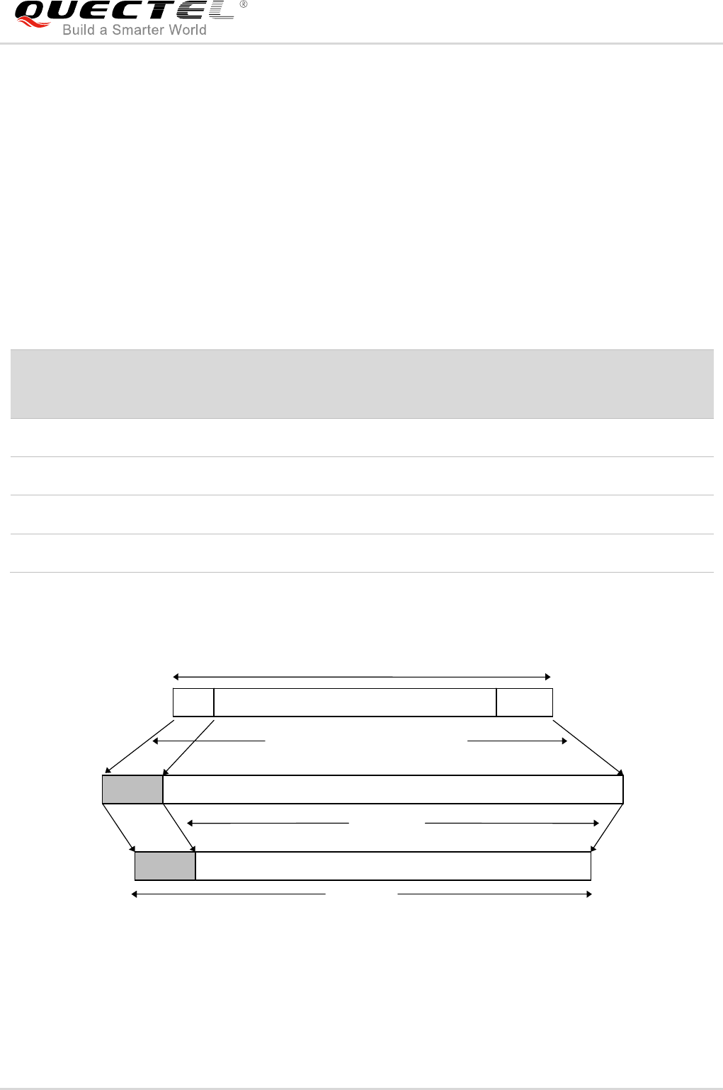
GSM/GPRS/GNSS Module Series
MC20 Hardware Design
MC20_Hardware_Design Confidential / Released 93 / 95
9 Appendix B GPRS Coding Schemes
Four coding schemes are used in GPRS protocol. The differences between them are shown in the
following table.
Table 43: Description of Different Coding Schemes
Scheme Code
Rate USF Pre-coded
USF
Radio Block
excl.USF and
BCS
BCS Tail Coded
Bits
Punctured
Bits
Data
Rate
Kb/s
CS-1 1/2 3 3 181 40 4 456 0 9.05
CS-2 2/3 3 6 268 16 4 588 132 13.4
CS-3 3/4 3 6 312 16 4 676 220 15.6
CS-4 1 3 12 428 16 - 456 - 21.4
Radio block structure of CS-1, CS-2 and CS-3 is shown as the figure below.
Figure 50: Radio Block Structure of CS-1, CS-2 and CS-3
Rate 1/2 convolutional coding
Puncturing
456 bits
USF BCS
Radio Block

GSM/GPRS/GNSS Module Series
MC20 Hardware Design
MC20_Hardware_Design Confidential / Released 94 / 95
Radio block structure of CS-4 is shown as the following figure.
Figure 51: Radio Block Structure of CS-4
Block
Code No coding
456 bits
USF BCS
Radio Block

GSM/GPRS/GNSS Module Series
MC20 Hardware Design
MC20_Hardware_Design Confidential / Released 95 / 95
10 Appendix C GPRS Multi-slot Classes
Twenty-nine classes of GPRS multi-slot modes are defined for MS in GPRS specification. Multi-slot
classes are product dependent, and determine the maximum achievable data rates in both the uplink and
downlink directions. Written as 3+1 or 2+2, the first number indicates the amount of downlink timeslots,
while the second number indicates the amount of uplink timeslots. The active slots determine the total
number of slots the GPRS device can use simultaneously for both uplink and downlink communications.
The description of different multi-slot classes is shown in the following table.
Table 44: GPRS Multi-slot Classes
Multislot Class Downlink Slots Uplink Slots Active Slots
1 1 1 2
2 2 1 3
3 2 2 3
4 3 1 4
5 2 2 4
6 3 2 4
7 3 3 4
8 4 1 5
9 3 2 5
10 4 2 5
11 4 3 5
12 4 4 5