Quectel Wireless Solutions 201706SC20A LTE Module User Manual
Quectel Wireless Solutions Company Limited LTE Module
Contents
- 1. User manual
- 2. Users Manual
- 3. User Manual
User manual

SC20-A Manual
LTE Module Series
Rev: SC20-A_Manual_R1.0
Date: 2017-06-30
www.quectel.com

SC20-A_Manual_R1.0 Confidential / Released 1 / 49
Our aim is to provide customers with timely and comprehensive service. For any
assistance, please contact our company headquarters:
Quectel Wireless Solutions Co., Ltd.
7th Floor, Hongye Building, No.1801 Hongmei Road, Xuhui District, Shanghai 200233, China
Tel: +86 21 5108 6236
Email: info@quectel.com
Or our local office. For more information, please visit:
http://www.quectel.com/support/salesupport.aspx
For technical support, or to report documentation errors, please visit:
http://www.quectel.com/support/techsupport.aspx
Or email to: Support@quectel.com
GENERAL NOTES
QUECTEL OFFERS THE INFORMATION AS A SERVICE TO ITS CUSTOMERS. THE INFORMATION
PROVIDED IS BASED UPON CUSTOMERS’ REQUIREMENTS. QUECTEL MAKES EVERY EFFORT
TO ENSURE THE QUALITY OF THE INFORMATION IT MAKES AVAILABLE. QUECTEL DOES NOT
MAKE ANY WARRANTY AS TO THE INFORMATION CONTAINED HEREIN, AND DOES NOT ACCEPT
ANY LIABILITY FOR ANY INJURY, LOSS OR DAMAGE OF ANY KIND INCURRED BY USE OF OR
RELIANCE UPON THE INFORMATION. THE INFORMATION SUPPLIED HEREIN IS SUBJECT TO
CHANGE WITHOUT PRIOR NOTICE.
COPYRIGHT
THE INFORMATION CONTAINED HERE IS PROPRIETARY TECHNICAL INFORMATION OF
QUECTEL CO., LTD. TRANSMITTING, REPRODUCTION, DISSEMINATION AND EDITING OF THIS
DOCUMENT AS WELL AS UTILIZATION OF THE CONTENT ARE FORBIDDEN WITHOUT
PERMISSION. OFFENDERS WILL BE HELD LIABLE FOR PAYMENT OF DAMAGES. ALL RIGHTS
ARE RESERVED IN THE EVENT OF A PATENT GRANT OR REGISTRATION OF A UTILITY MODEL
OR DESIGN.
Copyright © Quectel Wireless Solutions Co., Ltd. 2017. All rights reserved.

SC20-A_Manual_R1.0 Confidential / Released 2 / 49
About the Document
History
Revision
Date Author Description
1.0 2016-06-29 Nina Dou SC20-A_Manual_R1.0

SC20-A_Manual_R1.0 Confidential / Released 3 / 49
Contents
About the Document ................................................................................................................................... 2
Contents ....................................................................................................................................................... 3
1 Introduction .......................................................................................................................................... 5
1.1. Safety Information...................................................................................................................... 5
2 Product Concept .................................................................................................................................. 7
2.1. General Description ................................................................................................................... 7
2.2. Key Features ............................................................................................................................. 8
2.3. Functional Diagram ................................................................................................................. 10
2.4. Evaluation Board ..................................................................................................................... 11
3 Application Interfaces ....................................................................................................................... 12
3.1. General Description ................................................................................................................. 12
3.2. Pin Assignment ........................................................................................................................ 13
4 Wi-Fi and BT ....................................................................................................................................... 14
4.1. Wi-Fi Overview ........................................................................................................................ 14
4.1.1. Wi-Fi Performance ......................................................................................................... 14
4.2. BT Overview ............................................................................................................................ 15
4.2.1. BT Performance ............................................................................................................. 15
5 GNSS ................................................................................................................................................... 17
5.1. GNSS Performance ................................................................................................................. 17
6 Antenna Interface ............................................................................................................................... 18
6.1. Main/Rx-diversity Antenna Interface ........................................................................................ 18
6.1.1. Pin Definition .................................................................................................................. 18
6.1.2. Operating Frequency ..................................................................................................... 18
6.2. Wi-Fi/BT Antenna Interface ..................................................................................................... 20
6.3. GNSS Antenna Interface ......................................................................................................... 20
6.4. Antenna Installation ................................................................................................................. 21
6.4.1. Antenna Requirement .................................................................................................... 21
7 Electrical, Reliability and Radio Characteristics ............................................................................ 23
7.1. Absolute Maximum Ratings ..................................................................................................... 23
7.2. Power Supply Ratings ............................................................................................................. 23
7.3. Charging Performance Specifications ..................................................................................... 24
7.4. Operating Temperature ............................................................................................................ 24
7.5. Current Consumption .............................................................................................................. 25
7.6. Electrostatic Discharge ............................................................................................................ 34
8 Technical Dimensions ....................................................................................................................... 35
8.1. Mechanical Dimensions of the Module.................................................................................... 35
8.2. Recommended Footprint ......................................................................................................... 37

SC20-A_Manual_R1.0 Confidential / Released 4 / 49
8.3. Top and Bottom View of the Module ........................................................................................ 38
9 Storage, Manufacturing and Packaging .......................................................................................... 39
9.1. Storage..................................................................................................................................... 39
9.2. Manufacturing and Welding ..................................................................................................... 39
9.3. Packaging ................................................................................................................................ 41
10 Appendix A GPRS Coding Schemes ............................................................................................... 43
11 Appendix B GPRS Multi-slot Classes .............................................................................................. 44
12 Appendix C EDGE Modulation and Coding Schemes ................................................................... 45
13 CE Requirement ................................................................................................................................. 46
14 IC & FCC Requirement ...................................................................................................................... 47
14.1. FCC Regulations: .................................................................................................................... 47
14.2. RF Exposure Information ......................................................................................................... 47
14.3. ISED Notice ............................................................................................................................. 47
14.4. ISED Radiation Exposure Statement ...................................................................................... 48
14.5. IMPORTANT NOTE: ................................................................................................................ 48
14.6. USERS MANUAL OF THE END PRODUCT: .......................................................................... 48
14.7. LABEL OF THE END PRODUCT: ........................................................................................... 49

SC20-A_Manual_R1.0 Confidential / Released 5 / 49
1
Introduction
This document defines the SC20 module and describes its air interface and hardware interface which are
connected with your application.
1.1. Safety Information
Full attention must be given to driving at all times in order to reduce the risk of an
accident. Using a mobile while driving (even with a handsfree kit) causes
distraction and can lead to an accident. You must comply with laws and regulations
restricting the use of wireless devices while driving.
Switch off the cellular terminal or mobile before boarding an aircraft. Make sure it is
switched off. The operation of wireless appliances in an aircraft is forbidden, so as
to prevent interference with communication systems. Consult the airline staff about
the use of wireless devices on boarding the aircraft, if your device offers an
Airplane Mode which must be enabled prior to boarding an aircraft.
Switch off your wireless device when in hospitals or clinics or other health care
facilities. These requests are desinged to prevent possible interference with
sentitive medical equipment.
This document can help you quickly understand module interface specifications, electrical and
mechanical details as well as other related information of SC20 module. Associated with application notes
and user guide, you can use SC20 module to design and set up mobile applications easily.
The following safety precautions must be observed during all phases of operation, such as usage, service
or repair of any cellular terminal or mobile incorporating SC20 module. Manufacturers of the cellular
terminal should send the following safety information to users and operating personnel and to incorporate
these guidelines into all manuals supplied with the product. If not so, Quectel assumes no liability for the
customer’s failure to comply with these precautions.
SC20-A_Manual_R1.0 Confidential / Released 6 / 49
Cellular terminals or mobiles operating over radio frequency signal and cellular
network cannot be guaranteed to connect in all conditions, for example no mobile
fee or with an invalid SIM card. While you are in this condition and need emergent
help, please remember using emergency call. In order to make or receive a call,
the cellular terminal or mobile must be switched on and in a service area with
adequate cellular signal strength.
Your cellular terminal or mobile contains a transmitter and receiver. When it is ON ,
it receives and transmits radio frequency energy. RF interference can occur if it is
used close to TV set, radio, computer or other electric equipment.
In locations with potencially explosive atmospheres, obey all posted signs to turn
off wireless devices such as your phone or other cellular terminals. Areas with
potencially exposive atmospheres include fuelling areas, below decks on boats,
fuel or chemical transfer or storage facilities, areas where the air contains
chemicals or particles such as grain, dust or metal powders, etc.
Please do not discard. Maybe wireless devices have an impact on the environment
so please do not arbitrarily discarded.
The device is restricted to indoor use only when oparating in the 5150 to 5350 Mhz
frequency range.

SC20-A_Manual_R1.0 Confidential / Released 7 / 49
2
Product Concept
2.1. General Description
Table 1: SC20-A Frequency Bands
Type Frequency
LTE-FDD B2/B4/B5/B7/B12/B13/B25/B26
WCDMA B1/B2/B4/B5/B8
GSM 850/1900MHz
Wi-Fi 802.11a/b/g/n 2412-2472MHz;
5180-5825MHz
BT4.1 LE 2402-2480MHz
GNSS GPS/GLONASS/BeiDou
SC20 is a series of 4G smart modules based on Qualcomm platform and Android operating system, with
providing industrial grade performance. It supports worldwide LTE-FDD/LTE-TDD/WCDMA/TD-SCDMA/
EVDO/CDMA/GSM coverage, and also supports short-range wireless communication via
Wi-Fi 802.11a/b/g/n and BT4.1 LE. Additionally, SC20 integrates GPS/GLONASS/BeiDou satellite
positioning systems. Due to multiple speech and audio codecs as well as the built-in high performance
AdrenoTM 304 graphics processing unit, it enables smooth play of 720P videos. The module also offers
multiple audio and video input/output interfaces as well as abundant GPIO interfaces.
The following table shows the supported network types and frequency bands of SC20.
Including a series of product such as:SC20-CE,SC20-A,SC20-AU,SC20-E,SC20-J.
SC20 is an SMD type module, which can be embedded into applications through its 210-pin pads
including 146 LCC signal pads and 64 other pads. With a compact profile of 40.5mm × 40.5mm × 2.8mm,
SC20 can meet almost all requirements for M2M applications such as CPE,automotive, smart metering,
tracking, security, routers, wireless POS, mobile computing devices, PDA phone, tablet PC, etc.

SC20-A_Manual_R1.0 Confidential / Released 8 / 49
2.2. Key Features
The following table describes the detailed features of SC20 module.
Table 2: SC20 Key Features
Feature Details
Applications Processor ARM Cortex-A7 microprocessor cores (quad-core) up to 1.1 GHz
512KB L2 cache
Modem DSP QDSP6 v5 core up to 691.2 MHz
768KB L2 cache
Memory 8GB EMMC+8Gb LPDDR3
Operating System Android OS 5.1
Power Supply Supply voltage: 3.5V~4.2V
Typical supply voltage: 3.8V
LTE Features
Support 3GPP R10 CAT4 FDD and TDD
Support 1.4 to 20 MHz RF bandwidth
Support DL 2 x 2 MIMO
FDD data rate: Max 150Mbps (DL), 50Mbps (UL)
TDD data rate: Max 130Mbps (DL), 35Mbps (UL)
WCDMA Features
Support 3GPP R8 DC-HSPA+
Support 16-QAM, 64-QAM and QPSK modulation
3GPP R6 HSUPA: Max 5.76Mbps (UL)
3GPP R8 DC-HSPA+: Max 42Mbps (DL)
TD-SCDMA Features Support CCSA Release 3
Max 4.2Mbps (DL), 2.2Mbps (UL)
CDMA Features Max 3.1Mbps (DL), 1.8Mbps (UL)
GSM/GPRS/EDGE
Data Features
GPRS
Support GPRS multi-slot class 33
Coding scheme: CS-1, CS-2, CS-3 and CS-4
Maximum of four Rx time slots per frame
EDGE
Support EDGE multi-slot class 33
Support GMSK and 8-PSK
WLAN Features
Support 2.4G and 5G frequency band, (SC20-CE does not support 5G
frequency).
Support 802.11a/b/g/n, data rate up to 150Mbps
Support AP mode;
Bluetooth Feature BT4.1 LE

SC20-A_Manual_R1.0 Confidential / Released 9 / 49
GNSS Features GPS/GLONASS/BeiDou
SMS
Text and PDU mode
Point to point MO and MT
SMS cell broadcast
SMS storage: ME by default
AT Commands Compliant with 3GPP TS 27.007, 27.005 and Quectel enhanced AT
commands
LCM Interface
4 lanes MIPI_DSI, up to 1.5Gbps each
Support WVGA (2 lanes MIPI_DSI), up to 720p (4 lanes MIPI_DSI)
24bit color depth
Camera Interface
Use MIPI_CSI, up to 1.5Gbps per lane, support two cameras
2-lane MIPI_CSI for rear camera, up to 8MP
1-lane MIPI_CSI for front camera, up to 2MP
Audio Interface
Audio input
2 groups analog microphone input, integrate internal bias voltage
Audio output
Class AB stereo headphone output
Class AB earpiece differential output
Class D speaker differential amplifier output
USB Interface
Compliant with USB 2.0 specification; the data transfer rate can reach
up to 480Mbps
Used for AT command communication, data transmission, software
debugging and firmware upgrade
Support USB OTG (Need additional 5V power supply chip)
USB Driver: Support Windows XP, Windows Vista, Windows 7,
Windows 8, Windows CE5.0/6.0*, Linux 2.6/3.0, Android 2.3/4.0/4.2
USIM Interface 2 groups of USIM interface
Support USIM/SIM card: 1.8V, 3.0V
UART Interface
2 groups of UART interface
4-wire UART interface with RTS and CTS hardware flow control
2-wire UART interface for software debugging
Baud rate up to 4Mbps
SDIO Interface Support SD3.0; 4bit SDIO; SD Card
Support hot plug
I2C Interface 3 groups I2C, used for TP, camera, sensor peripherals, etc.
ADC Interface Support 3 ADC interfaces,used for input voltage sense, battery
temperature detection and general purpose ADC
Real Time Clock Implemented
Antenna Interface MAIN antenna, DRX antenna, GNSS antenna and Wi-Fi/BT antenna
Physical Characteristics Size: 40.5±0.15 × 40.5±0.15 × 2.8±0.2 mm
Interface: LCC
SC20-A_Manual_R1.0 Confidential / Released 10 / 49
Weight: approx. 9.6g
Temperature Range Operating temperature range: -35°C~+65°C 1)
Extended temperature range : -40°C~+75°C 2)
Firmware Upgrade Over USB interface
RoHS All hardware components are fully compliant with EU RoHS directive
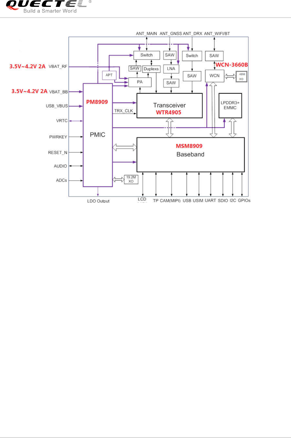
2.3. Functional Diagram
Power management
Radio frequency
Baseband
LPDDR3+EMMC flash
Peripheral interface
--USB interface
--USIM interface
--UART interface
--SDIO interface
--I2C interface
--ADC interface
--LCD (MIPI) interface
--TP interface
--CAM (MIPI) interface
--AUDIO interface
1) Within operation temperature range, the module is 3GPP compliant.
2) Within extended temperature range, the module remains the ability to establish and maintain a voice,
SMS, data transmission, emergency call, etc. There is no unrecoverable malfunction. There are also no
effects on radio spectrum and no harm to radio network. Only one or more parameters like Pout might
reduce in their value and exceed the specified tolerances. When the temperature returns to the normal
operating temperature levels, the module will meet 3GPP compliant again.
* means this feature is under development.
The following figure shows a block diagram of SC20 and illustrates the major functional parts.
NOTES
SC20-A_Manual_R1.0 Confidential / Released 11 / 49
Figure 1: Functional Diagram
2.4. Evaluation Board
In order to help you to develop applications with SC20, Quectel supplies an evaluation board
(SMART-EVB), RS-232 to USB cable, USB data cable, power adapter, earphone, antenna and other
peripherals to control or test the module. For details, please refer to document [1].

SC20-A_Manual_R1.0 Confidential / Released 12 / 49
3
Application Interfaces
3.1. General Description
Power supply
VRTC interface
LCM interface
TP interface
Camera interface
Audio interface
USB interface
USIM interface
UART interface
SDIO interface
I2C interface
ADC interface
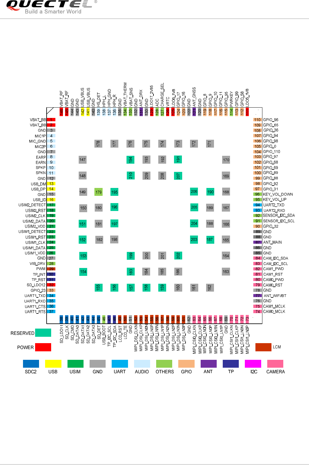
SC20 is equipped with 146-pin 1.0mm pitch SMT pads plus 64-pin ground pads and reserved pads that
can be embedded into cellular application platform. The following chapters provide the detailed
description of pins/interfaces listed below.
SC20-A_Manual_R1.0 Confidential / Released 13 / 49
3.2. Pin Assignment
The following figure shows the pin assignment of SC20 module.
Figure 2: Pin Assignment (Top View)
SC20-A_Manual_R1.0 Confidential / Released 14 / 49
4
Wi-Fi and BT
4.1. Wi-Fi Overview
4.1.1. Wi-Fi Performance
Referenced specifications are listed below:
No. Document
1 IEEE 802.11n WLAN MAC and PHY, October 2009 + IEEE 802.11-2007 WLAN MAC and
PHY, June 2007
SC20 module provides a shared antenna interface ANT_WIFI/BT for Wi-Fi and Bluetooth (BT) functions.
The interface impedance is 50Ω. External antennas such as dipole antenna can be connected to the
module via the interface, so as to achieve Wi-Fi and BT functions.
SC20 module supports 2.4G and 5G double-band WLAN wireless communication based on IEEE 802.11
a/802.11b/ 802.11g/ 802.11n standard protocols. The maximum data rate is up to 150 Mbps.
The features are as below:
Support Wake-on-WLAN (WoWLAN)
Support ad hoc mode
Support WAPI SMS4 hardware encryption
Support AP mode
Support Wi-Fi Direct
Support MCS 0-7 for HT20 and HT40
SC20-CE only supports 2.4G single band WIFI, and does not support 802.11a.
The following table lists the Wi-Fi transmitting and receiving performance of SC20 module (SC20-CE
does not support 5G frequency band).
NOTE

SC20-A_Manual_R1.0 Confidential / Released 15 / 49
2 IEEE Std 802.11b, IEEE Std 802.11d, IEEE Std 802.11e, IEEE Std 802.11g, IEEE Std
802.11i: IEEE 802.11-2007 WLAN MAC and PHY, June 2007
4.2. BT Overview
Supports max. 7 wireless connections.
Supports max. 3.5 piconets at the same time.
Supports one SCO (Synchronous Connection Oriented) or eSCO connection.
Table 3: BT Data Rate and Version
Version Data rate Maximum Application Throughput Comment
1.2 1 Mbit/s >80 Kbit/s
2.0 + EDR 3 Mbit/s >80 Kbit/s
3.0 + HS 24 Mbit/s Reference 3.0 + HS
4.0 24 Mbit/s Reference 4.0 LE
Referenced specifications are listed below:
No. Document
1 Bluetooth Radio Frequency TSS and TP Specification 1.2/2.0/2.0 + EDR/2.1/2.1+ EDR/3.0/3.0
+ HS, August 6, 2009
2 Bluetooth Low Energy RF PHY Test Specification, RF-PHY.TS/4.0.0, December 15, 2009
4.2.1. BT Performance
Table 4: BT Transmitting and Receiving Performance
Transmitter Performance
SC20 module supports BT4.1 (BR/EDR+BLE) specification, as well as GFSK, 8-DPSK, π/4-DQPSK
modulation modes.
The BR/EDR channel bandwidth is 1MHz, and can accommodate 79 channels. The BLE channel
bandwidth is 2MHz, and can accommodate 40 channels.
The following table lists the BT transmitting and receiving performance of SC20 module.

SC20-A_Manual_R1.0 Confidential / Released 16 / 49
Packet Types DH5 2-DH5 3-DH5
Transmitting Power 10dBm 8dBm 8dBm
Receiver Performance
Packet Types DH5 2-DH5 3-DH5
Receiving Sensitivity -92dBm -91dBm -86dBm

SC20-A_Manual_R1.0 Confidential / Released 17 / 49
5
GNSS
5.1. GNSS Performance
Table 5: GNSS Performance
Parameter Description Typ. Unit
Sensitivity (GNSS)
Cold start -146 dBm
Reacquisition -158 dBm
Tracking -160 dBm
TTFF (GNSS)
Cold start 32 s
Warm start 30 s
Hot start 2 s
Static Drift (GNSS) CEP-50 6 m
SC20 module integrates a Qualcomm IZat™ GNSS engine (GEN 8C) which supports multiple positioning
and navigation systems including GPS, GLONASS and BeiDou. With an embedded LNA, the module
provides greatly improved positioning accuracy.
The following table lists the GNSS performance of SC20 module in conduction mode.

SC20-A_Manual_R1.0 Confidential / Released 18 / 49
6
Antenna Interface
6.1. Main/Rx-diversity Antenna Interface
6.1.1. Pin Definition
Table 6: Pin Definition of the Main/Rx-diversity Antenna
Pin Name Pin No. I/O Description Comment
ANT_MAIN 87 IO Main antenna 50Ω impedance
6.1.2. Operating Frequency
Table 7: SC20 Module Operating Frequencies
3GPP Band Receive Transmit Unit
GSM850 869-894 824-849 MHz
EGSM900 925-960 880-915 MHz
DCS1800 1805-1880 1710-1785 MHz
PCS1900 1930-1990 1850-1910 MHz
WCDMA Band 1 2110-2170 1920-1980 MHz
WCDMA Band 2 1930-1990 1850-1910 MHz
SC20 antenna interface includes a main antenna, an Rx-diversity/MIMO antenna, a GNSS antenna and a
Wi-Fi/BT antenna. The antenna interface has an impedance of 50Ω.
The main antenna and Rx-diversity antenna pins’ definition are shown below.
ANT_DRX 131 AI Diversity antenna 50Ω impedance

SC20-A_Manual_R1.0 Confidential / Released 19 / 49
WCDMA Band 4 2110-2155 1710-1755 MHz
WCDMA Band 5 869-894 824-849 MHz
WCDMA Band 6 875-885 830-840 MHz
WCDMA Band 8 925-960 880-915 MHz
WCDAM Band 19 875-890 830-845 MHz
CDMA BC0 869-894 824-849 MHz
TD-SCDMA Band 34 2010-2025 2010-2025 MHz
TD-SCDMA Band 39 1880-1920 1880-1920 MHz
LTE-FDD Band 1 2110-2170 1920-1980 MHz
LTE-FDD Band 2 1930-1990 1850-1910 MHz
LTE-FDD Band 3 1805-1880 1710-1785 MHz
LTE-FDD Band 4 2110-2155 1710-1755 MHz
LTE-FDD Band 5 869-894 824-849 MHz
LTE-FDD Band 8 925-960 880-915 MHz
LTE-FDD Band 12 729-746 699-716 MHz
LTE-FDD Band 13 746-756 777-787 MHz
LTE-FDD Band 18 860-875 815-830 MHz
LTE-FDD Band 19 875-890 830-845 MHz
LTE-FDD Band 20 791-821 832-862 MHz
LTE-FDD Band 25 1930-1995 1850-1915 MHz
LTE-FDD Band 26 859-894 814-849 MHz
LTE-FDD Band 28 758-803 703-748 MHz
LTE-TDD Band 38 2570-2620 2570-2620 MHz
LTE-TDD Band 39 1880-1920 1880-1920 MHz
LTE-TDD Band 40 2300-2400 2300-2400 MHz
SC20-A_Manual_R1.0 Confidential / Released 20 / 49
LTE-TDD Band 41 2555-2655 2555-2655 MHz
6.2. Wi-Fi/BT Antenna Interface
Table 8: Pin Definition of Wi-Fi/BT Antenna
Pin Name Pin No. I/O Description Comment
ANT_WIFI/BT 77 IO Wi-Fi/BT antenna 50Ω impedance
Table 9: Wi-Fi/BT Frequency
Type Frequency Unit
Wi-Fi 802.11a/b/g/n 2412-2472MHz;
5180-5825MHz MHz
BT4.1 LE 2402-2480MHz MHz
6.3. GNSS Antenna Interface
The following tables show the GNSS antenna pin’s definition and frequency specification.
Table 10: Pin Definition of GNSS Antenna
Pin Name Pin No. I/O Description Comment
ANT_GNSS 121 AI GNSS antenna 50Ω impedance
The bandwidth of LTE-TDD Band 41 for SC20 module is 100MHz (2555 MHz - 2655 MHz), and the
corresponding channel range is from 40240 up to 41240.
The following tables show the Wi-Fi/BT antenna pin’s definition and frequency specification.
NOTE

SC20-A_Manual_R1.0 Confidential / Released 21 / 49
Table 11: GNSS Frequency
Type Frequency Unit
GPS 1575.42 ± 1.023 MHz
GLONASS 1597.5 - 1605.8 MHz
BeiDou 1561.098 ± 2.046 MHz
6.4. Antenna Installation
6.4.1. Antenna Requirement
Table 12: Antenna Requirements
Type Requirements
GSM/WCDMA/TD-SCDMA/LTE
VSWR: ≤ 2
Max Input Power (W): 50
Input Impedance (Ω): 50
Polarization Type: Vertical
Cable Insertion Loss: < 1dB
(GSM850,EGSM900,WCDMA B5/B6/B8/B19,CDMA BC0,LTE-FDD
B5/B8/B12/B13/B18/B19/B20/B26/B28)
Cable Insertion Loss: < 1.5dB
(DCS1800, PCS1900,WCDMA B1/B2/B4, TD-SCDMA B34/B39,
LTE-FDD B1/B2/B3/B4/B25,LTE-TDD B39)
Cable Insertion Loss: < 2dB
(LTE-FDD B7,LTE-TDDB38/B40/B41)
Wi-Fi/BT
VSWR: ≤ 2
Max Input Power (W): 50
Input Impedance (Ω): 50
Polarization Type: Vertical
Cable Insertion Loss: < 1dB
GNSS
Frequency range: 1565 - 1607MHz
Polarization: RHCP or linear
VSWR: < 2 (Typ.)
Passive Antenna Gain: > 0dBi
Active Antenna Noise Figure: < 1.5dB
The following table shows the requirement on main antenna, RX-diversity antenna, Wi-Fi/BT antenna and
GNSS antenna.
SC20-A_Manual_R1.0 Confidential / Released 22 / 49
Active Antenna Gain: > -2dBi
Active Antenna Embedded LNA Gain: 20dB (Typ.)
Active Antenna Total Gain: > 18dBi (Typ.)
Table 13: Antenna Gain
Conclusion:
The analysis concludes that this product when transmitting in standalone within a host device, is
compliant with the RF exposure requirements in mobile exposure condition, provided the conducted
power and antenna gain do not exceed the limits for each given frequency band per wireless technology
as follow table:
Technology Band Maximum
Conducted Power (dBm) Maximum Antenna Gain (dBi)
GSM GSM850 33.0 3.0
GSM1900 30.5 2.5
WCDMA
Band II 24.0 2.5
Band IV 24.0 5.0
Band V 24.0 3.0
LTE
Band 2 24.0 2.5
Band 4 24.5 5.0
Band 5 24.5 3.0
Band 7 24.5 8.5
Band 12 24.0 6.0
Band 13 24.0 6.0
Band 25 24.0 2.5
Band 26 24.0 3.0
Note: The WiFi2.4GHz/WiFi5GHz/Bluetooth dipole antenna information as below:
Manufacturer Model Peak gain
INPAQ TECHNOLOGY CO., LTD
DAM-L0-H-N0-000-08-13
WiFi2.4GHz/Bluetooth: 3.0 dBi
WiFi5GHz: 4.0 dBi

SC20-A_Manual_R1.0 Confidential / Released 23 / 49
7
Electrical, Reliability and Radio
Characteristics
7.1. Absolute Maximum Ratings
Table 14: Absolute Maximum Ratings
Parameter Min. Max. Unit
VBAT -0.5 6 V
USB_VBUS -0.5 16 V
Peak Current of VBAT 0 3 A
Voltage on Digital Pins -0.3 2.3 V
7.2. Power Supply Ratings
Table 15: SC20 Module Power Supply Ratings
Parameter Description Conditions Min. Typ. Max. Unit
VBAT
VBAT
Voltage must stay within the
min/max values, including
voltage drop, ripple and spikes.
3.5 3.8 4.2 V
Voltage drop
during transmitting
burst
Maximum power control level
on EGSM900. 400 mV
IVBAT
Peak supply
current (during
transmission slot)
Maximum power control level
on EGSM900. 1.8 3.0 A
Absolute maximum ratings for power supply and voltage on digital and analog pins of the module are
listed in the following table.
SC20-A_Manual_R1.0 Confidential / Released 24 / 49
Parameter Description Conditions Min. Typ. Max. Unit
USB_VBUS
USB detection 4.35 5.0 6.3 V
VRTC Power supply voltage
of backup battery. 2.0 3.0 3.25 V
7.3. Charging Performance Specifications
Table 16: Charging Performance Specifications
Parameter Min. Typ. Max. Unit
Trickle charging current 81 90 99 mA
Charge voltage range (25mV steps) 4 4.2 4.775 V
Charge voltage accuracy +/-2 %
Charge current range (90mA steps) 90 1440 mA
Charge current accuracy +/-10 %
Charge termination current: when charge
current is from 90 to 450mA; 7 %
Charge termination current: when charge
current is from 450 to 1440mA; 7.4 %
7.4. Operating Temperature
The operating temperature is listed in the following table.
Table 17: Operating Temperature
Parameter Min. Typ. Max. Unit
Operating temperature range 1)
-35 +25 +65 ºC
Extended temperature range 2)
-40 +75 ºC
Trickle charging threshold voltage range
(15.62mV steps) 2.5 2.796 2.984 V
Weak battery threshold voltage range
(18.75mV steps) 3.0 3.2 3.581 V

SC20-A_Manual_R1.0 Confidential / Released 25 / 49
1. 1) Operating temperature range ---- 3GPP compliant.
2) Within extended temperature range, the module remains the ability to establish and maintain a voice,
SMS, data transmission, emergency call, etc. There is no unrecoverable malfunction. There are also no
effects on radio spectrum and no harm to radio network. Only one or more parameters like Pout might
reduce in their value and exceed the specified tolerances. When the temperature returns to the normal
operating temperature levels, the module will meet 3GPP compliant again.
7.5. Current Consumption
Table 18: SC20-CE Current Consumption
Parameter
Description Conditions Typ. Unit
IVBAT
OFF state Power down 80 uA
GSM/GPRS supply
current
Sleep
@DRX=2 3.85 mA
Sleep
@DRX=5 3.01 mA
Sleep
@DRX=9 2.91 mA
WCDMA supply
current
Sleep
@DRX=6 3.30 mA
Sleep
@DRX=7 2.79 mA
Sleep
@DRX=8 2.49 mA
Sleep
@DRX=9 2.33 mA
LTE-FDD supply
current
Sleep
@DRX=5 5.60 mA
Sleep
@DRX=6 3.83 mA
Sleep
@DRX=7 3.02 mA
Sleep
@DRX=8 2.65 mA
The values of current consumption are shown below.
NOTES

SC20-A_Manual_R1.0 Confidential / Released 26 / 49
Parameter
Description Conditions Typ. Unit
LTE-TDD supply
current
Sleep
@DRX=5 5.49 mA
Sleep
@DRX=6 3.87 mA
Sleep
@DRX=7 3.05 mA
Sleep
@DRX=8 2.67 mA
GSM voice call
GSM900 PCL=5@31.84dBm 253.6 mA
GSM900 PCL=12@18.49dBm 142.9 mA
GSM900 PCL=19@4.95dBm 117.8 mA
DCS1800 PCL=0@28.91dBm 200.9 mA
DCS1800 PCL=7@15.35dBm 157 mA
DCS1800 PCL=15@-0.21dBm
138.1 mA
CDMA voice call
BC0(max power)
@23.91dBm 619.8 mA
BC0(min power)
@-60.28dBm 128.7 mA
WCDMA voice call
Band1(max power)
@22.61dBm 430 mA
Band8(max power)
@22.74dBm 392.2 mA
EDGE data transfer
EDGE900 (1UL/4DL)
@26.29dBm 193 mA
EDGE900 (2UL/3DL)
@26.15dBm 277.9 mA
EDGE900 (3UL/2DL)
@26.06dBm 362.2 mA
EDGE900 (4UL/1DL)
@25.92dBm 450.5 mA
DCS1800 (1UL/4DL)
@24.89dBm 183.5 mA
DCS1800 (2UL/3DL)
@24.74dBm 275.2 mA

SC20-A_Manual_R1.0 Confidential / Released 27 / 49
Parameter
Description Conditions Typ. Unit
DCS1800 (3UL/2DL)
@24.54dBm 355.9 mA
DCS1800 (4UL/1DL)
@24.44dBm 440.3 mA
CDMA data transfer
BC0(max power)
@23.68dBm 602.5 mA
WCDMA data
transfer
Band 1(HSDPA) @21.64dBm
461.5 mA
Band 8(HSDPA) @21.61dBm 423.8 mA
Band 1(HSUPA) @21.36dBm 452.5 mA
Band 8(HSUPA) @21.56dBm 436 mA
LTE data transfer
LTE-FDD Band1 @22.96dBm 631.2 mA
LTE-FDD Band3@22.95dBm 639.6 mA
LTE-FDD Band8 @23.17dBm 542 mA
LTE-TDD Band38 @22.02dBm
422.89 mA
LTE-TDD Band39 @22.13dBm
458 mA
LTE-TDD Band40 @22.01dBm
392.9 mA
LTE-TDD Band41 @22.31dBm
441.4 mA
Table 19: SC20-E Current Consumption
Parameter
Description Conditions Typ. Unit
IVBAT
OFF state Power down 80 uA
GSM/GPRS supply current
Sleep
@DRX=2 3.38 mA
Sleep
@DRX=5 2.31 mA
Sleep
@DRX=9 1.98 mA
WCDMA supply current Sleep
@DRX=6 2.77 mA

SC20-A_Manual_R1.0 Confidential / Released 28 / 49
Parameter
Description Conditions Typ. Unit
Sleep
@DRX=7 2.17 mA
Sleep
@DRX=8 1.90 mA
Sleep
@DRX=9 1.72 mA
LTE-FDD supply current
Sleep
@DRX=5 5.49 mA
Sleep
@DRX=6 3.06 mA
Sleep
@DRX=7 2.37 mA
Sleep
@DRX=8 1.91 mA
LTE-TDD supply current
Sleep
@DRX=5 5.51 mA
Sleep
@DRX=6 3.45 mA
Sleep
@DRX=7 2.40 mA
Sleep
@DRX=8 1.85 mA
GSM voice call
Sleep
PCL=5@32.79dBm 255 mA
GSM850
PCL=12@19.04dBm 135 mA
GSM850
PCL=19@5.37dBm 108 mA
EGSM900
PCL=5@32.95dBm 264 mA
EGSM900
PCL=12@19.23dBm 137 mA
EGSM900
PCL=19@5.71dBm 109 mA
DCS1800
PCL=0@29.74dBm 197 mA
DCS1800
PCL=7@16.31dBm 153 mA
DCS1800
PCL=15@0.48dBm 131 mA

SC20-A_Manual_R1.0 Confidential / Released 29 / 49
Parameter
Description Conditions Typ. Unit
PCS1900
PCL=0@29.78dBm 192 mA
PCS1900
PCL=7@16.73dBm 152 mA
PCS1900
PCL=15@0.66dBm 130 mA
WCDMA voice call
Band 1(max power)
@23.10dBm 521 mA
Band 5(max power)
@23.32dBm 504 mA
Band 8(max power)
@23.26dBm 536 mA
GPRS data transfer
GPRS850 (1UL/4DL)
@32.83dBm 260 mA
GPRS850 (2UL/3DL)
@32.72dBm 422 mA
GPRS850 (3UL/2DL)
@30.71dBm 491 mA
GPRS850 (4UL/1DL)
@29.59dBM 571 mA
GPRS900 (1UL/4DL)
@33.02dBm 272 mA
GPRS900 (2UL/3DL)
@32.87dBm 443 mA
GPRS900 (3UL/2DL)
@30.84dBm 510 mA
GPRS900 (4UL/1DL)
@29.77dBm 599 mA
DCS1800 (1UL/4DL)
@29.74dBm 204 mA
DCS1800 (2UL/3DL)
@29.63dBm 306 mA
DCS1800 (3UL/2DL)
@29.48dBm 415 mA
DCS1800 (4UL/1DL)
@29.64dBm 517 mA
PCS1900 (1UL/4DL)
@29.75dBm 197 mA
PCS1900 (2UL/3DL)
@29.63dBm 297 mA

SC20-A_Manual_R1.0 Confidential / Released 30 / 49
Parameter
Description Conditions Typ. Unit
PCS1900 (3UL/2DL)
@29.48dBm 396 mA
PCS1900 (4UL/1DL)
@29.30dBm 503 mA
EDGE data transfer
EDGE850 (1UL/4DL)
@26.71dBm 175 mA
EDGE850 (2UL/3DL)
@26.73dBm 268 mA
EDGE850 (3UL/2DL)
@26.62dBm 259 mA
EDGE850 (4UL/1DL)
@26.54dBm 451 mA
EDGE900 (1UL/4DL)
@27.05dBm 182 mA
EDGE900 (2UL/3DL)
@26.99dBm 281 mA
EDGE900 (3UL/2DL)
@27.07dBm 374 mA
EDGE900 (4UL/1DL)
@26.84dBm 476 mA
DCS1800 (1UL/4DL)
@25.56dBm 178 mA
DCS1800 (2UL/3DL)
@25.69dBm 263 mA
DCS1800 (3UL/2DL)
@25.56dBm 352 mA
DCS1800 (4UL/1DL)
@25.30dBm 446 mA
PCS1900 (1UL/4DL)
@26.08dBm 120 mA
PCS1900 (2UL/3DL)
@25.91dBm 231 mA
PCS1900 (3UL/2DL)
@25.92dBm 347 mA
PCS1900 (4UL/1DL)
@25.66dBm 464 mA
WCDMA data transfer
Band 1(HSDPA)
@22.23dBm 491 mA
Band 5(HSDPA)
@22.43dBm 476 mA

SC20-A_Manual_R1.0 Confidential / Released 31 / 49
Parameter
Description Conditions Typ. Unit
Band 8(HSDPA)
@22.34dBm 491 mA
Band 1(HSUPA)
@21.62dBm 486 mA
Band 5(HSUPA)
@22.12dBm 467 mA
Band 8(HSUPA)
@21.82dBm 492 mA
LTE data transfer
LTE-FDD Band1
@22.71dBm 690 mA
LTE-FDD
Band3@23.42dBm 699 mA
LTE-FDD
Band5@23.64dBm 684 mA
LTE-FDD Band7
@22.98dBm 868 mA
LTE-FDD Band8
@23.59dBm 681 mA
LTE-FDD Band20
@23.48dBm 692 mA
LTE-TDD Band38
@23.21dBm 500 mA
LTE-TDD Band40
@23.28dBm 449 mA
LTE-TDD Band41
@23.00dBm 481 mA
Table 20: SC20-A Current Consumption
Parameter
Description Conditions Typ. Unit
IVBAT
OFF state Power down 16 uA
GSM/GPRS supply current
Sleep @DRX=2 3.45 mA
Sleep @DRX=5 2.53 mA
Sleep @DRX=9 2.27 mA
WCDMA supply current
Sleep @DRX=6 3.16 mA
Sleep @DRX=7 2.27 mA

SC20-A_Manual_R1.0 Confidential / Released 32 / 49
Parameter
Description Conditions Typ. Unit
Sleep @DRX=8 1.76 mA
Sleep @DRX=9 1.78 mA
GSM voice call
GSM850PCL=5@32.48dBm 253.09 mA
GSM850PCL=12@19.35dBm
138.58 mA
GSM850PCL=19@5.47dBm 109.84 mA
PCS1900
PC=L0@30.08dBm 202.50 mA
PCS1900
PCL=7@16.86dBm 157.92 mA
PCS1900
PCL=15@1.13dBm 135.44 mA
WCDMA voice call
Band 1(max power)
@23.69dBm 547.75 mA
Band 2(max power)
@23.90dBm 576.08 mA
Band 4(max power)
@23.65dBm 537.20 mA
Band 5(max power)
@23.47dBm 533.06 mA
Band 8(max power)
@23.76dBm 557.79 mA
GPRS data transfer
GPRS850 (1UL/4DL)
@32.38dBm 254.25 mA
GPRS850 (2UL/3DL)
@32.04dBm 411.18 mA
GPRS850 (3UL/2DL)
@30.54dBm 493.74 mA
GPRS850 (4UL/1DL)
@29.54dBm 580.68 mA
PCS1900 (1UL/4DL)
@29.99dBm 205.51 mA
PCS1900 (2UL/3DL)
@29.84dBm 315.56 mA
PCS1900 (3UL/2DL)
@29.16dBm 407.30 mA
PCS1900 (4UL/1DL)
@29.24dBm 509.25 mA

SC20-A_Manual_R1.0 Confidential / Released 33 / 49
Parameter
Description Conditions Typ. Unit
EDGE data transfer
EDGE850 (1UL/4DL)
@26.80dBm 173.67 mA
EDGE850 (2UL/3DL)
@26.69dBm 268.78 mA
EDGE850 (3UL/2DL)
@26.52dBm 360.92 mA
EDGE850 (4UL/1DL)
@26.41dBm 459.33 mA
PCS1900 (1UL/4DL)
@25.96dBm 174.92 mA
PCS1900 (2UL/3DL)
@25.80dBm 269.30 mA
PCS1900 (3UL/2DL)
@25.56dBm 360.28 mA
PCS1900 (4UL/1DL)
@25.40dBm 462 mA
WCDMA data transfer
Band 1(HSDPA) @22.7dBm 487.87 mA
Band 2(HSDPA) @22.90dBm
539 mA
Band 4(HSDPA) @22.73dBm
495.49 mA
Band 5(HSDPA) @22.73dBm
497.11 mA
Band 8(HSDPA) @22.74dBm
499.5 mA
Band 1(HSUPA) @22.03dBm
496.03 mA
Band2(HSUPA) @22.57dBm
534 mA
Band 4(HSUPA) @22.24dBm
495.66 mA
Band 5(HSUPA) @22.1dBm 494.12 mA
Band 8(HSUPA) @22.02dBm
489.2 mA
LTE data transfer
LTE-FDD Band2 @23.06dBm
765 mA
LTE-FDD Band4 @23.12dBm
758 mA
LTE-FDD Band5@23.5dBm
673.55 mA
LTE-FDD Band7@22.59dBm
790.28 mA
LTE-FDD Band12 @23.3dBm
674.84 mA

SC20-A_Manual_R1.0 Confidential / Released 34 / 49
Parameter
Description Conditions Typ. Unit
LTE-FDD Band13 @23.3dBm
674.84 mA
LTE-FDD Band25 @23.1dBm
760 mA
LTE-FDD Band26 @23.2dBm
731 mA
7.6. Electrostatic Discharge
Table 21: Electrostatic Discharge Characteristics ( Temperature: 25℃, Humidity: 45%)
The module is not protected against electrostatic discharge (ESD) in general. Consequently, it should be
subject to ESD handling precautions that are typically applied to ESD sensitive components. Proper ESD
handling and packaging procedures must be applied throughout the processing, handling and operation
of any application that incorporates the module.
The following table shows the module electrostatic discharge characteristics.
Tested Points Contact Discharge Air Discharge Unit
VBAT, GND +/-5 +/-10 KV
All Antenna Interfaces +/-5 +/-10 KV
USB Interfaces +/-0.5 +/-1 KV
Other Interfaces +/-0.5 +/-1 KV
SC20-A_Manual_R1.0 Confidential / Released 35 / 49
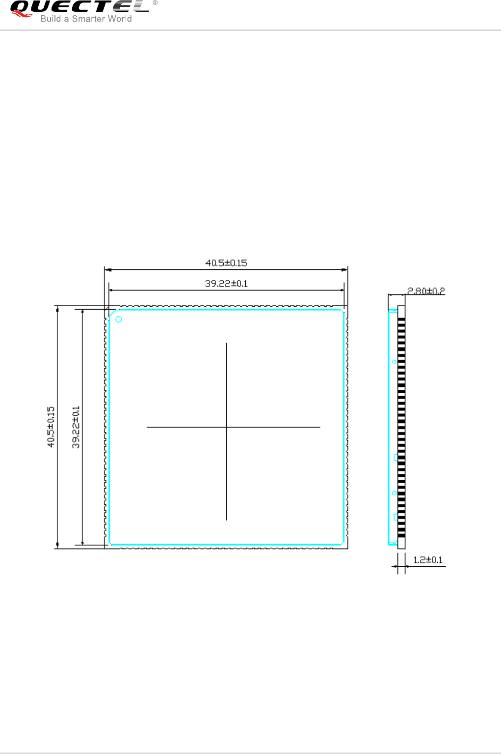
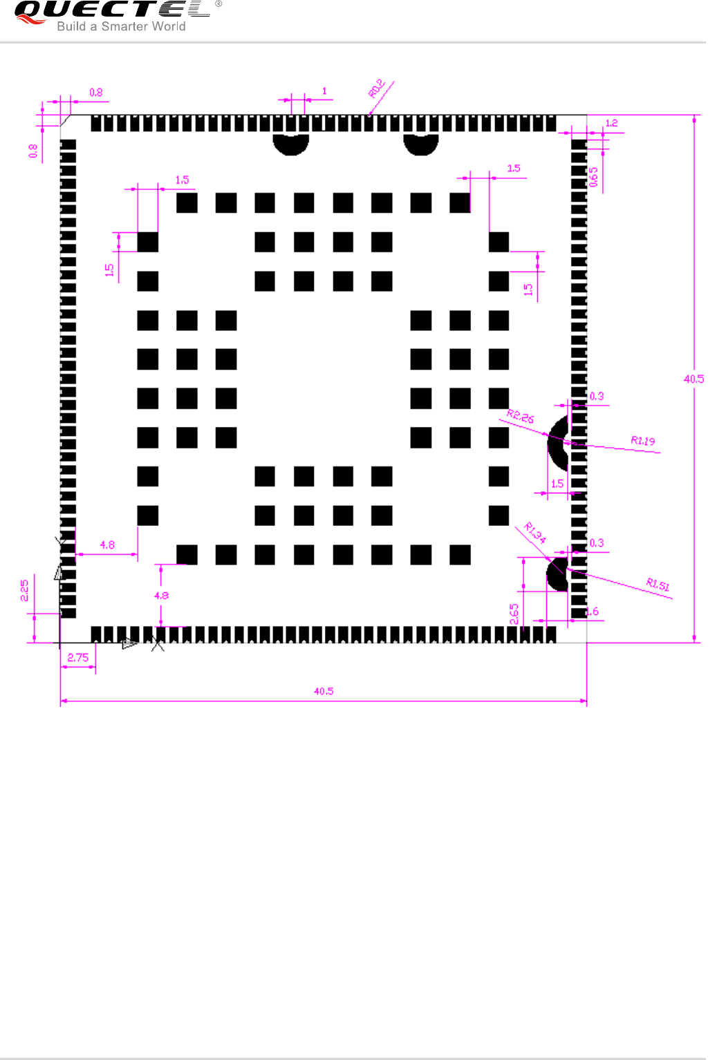
8
Technical Dimensions
This chapter describes the mechanical dimensions of the module. All dimensions are measured in mm.
8.1. Mechanical Dimensions of the Module
Figure 3: Module Top and Side Dimensions
SC20-A_Manual_R1.0 Confidential / Released 36 / 49
Figure 4: Module Bottom Dimensions (Top View)
SC20-A_Manual_R1.0 Confidential / Released 37 / 49
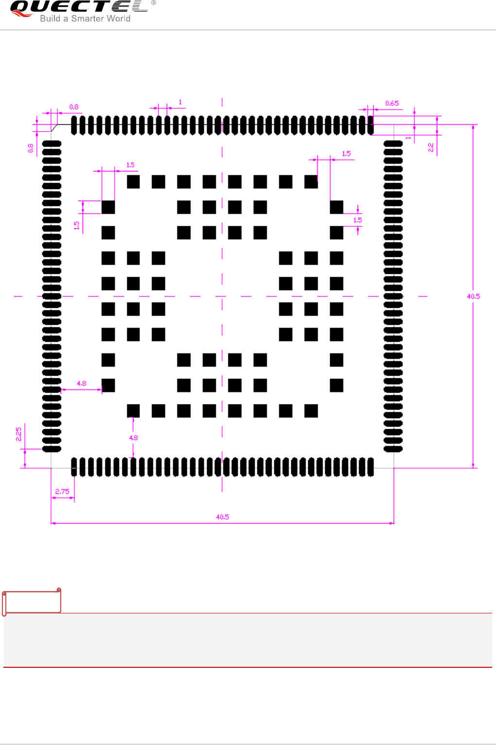
8.2. Recommended Footprint
Figure 5: Recommended Footprint (Top View)
1. For easy maintenance of the module, keep about 3mm between the module and other components in
the host PCB.
2. All RESERVED pins must not be connected to GND.
NOTES
SC20-A_Manual_R1.0 Confidential / Released 38 / 49
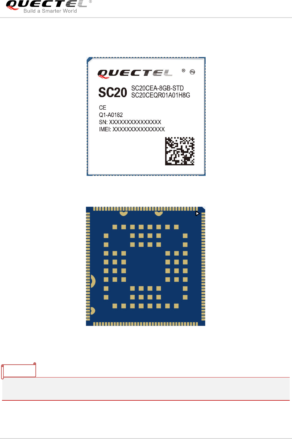
8.3. Top and Bottom View of the Module
Figure 6: Top View of the Module
Figure 7: Bottom View of the Module
These are design effect drawings of SC20 module. For more accurate pictures, please refer to the
module that you get from Quectel.
NOTE
SC20-A_Manual_R1.0 Confidential / Released 39 / 49
9
Storage, Manufacturing and
Packaging
9.1. Storage
SC20 is stored in a vacuum-sealed bag. The restrictions of storage condition are shown as below.
1. Shelf life in sealed bag is 12 months at < 40ºC/90%RH.
2. After this bag is opened, devices that will be subjected to reflow soldering or other high temperature
process must be:
Mounted within 72 hours at factory conditions of ≤ 30ºC/60%RH.
Stored at < 10% RH.
3. Devices require baking before mounting, if:
Humidity indicator card is > 10% when ambient temperature is 23ºC±5ºC.
Mounting cannot be finished within 72 hours at factory conditions of ≤ 30ºC/60% RH.
4. If baking is required, devices may be baked for 48 hours at 125ºC±5ºC.
9.2. Manufacturing and Welding
Push the squeegee to apply the solder paste on the surface of stencil, thus making the paste fill the
stencil openings and then penetrate to the PCB. The force on the squeegee should be adjusted properly
so as to produce a clean stencil surface on a single pass. To ensure the module soldering quality, the
thickness of stencil at the hole of the module pads should be 0.18mm. For details, please refer to
document [3].
As plastic package cannot be subjected to high temperatures, the package must be removed from
devices before high temperature (125ºC) baking. If shorter baking time is desired, please refer to
IPC/JEDECJ-STD-033 for baking procedure.
NOTE
SC20-A_Manual_R1.0 Confidential / Released 40 / 49
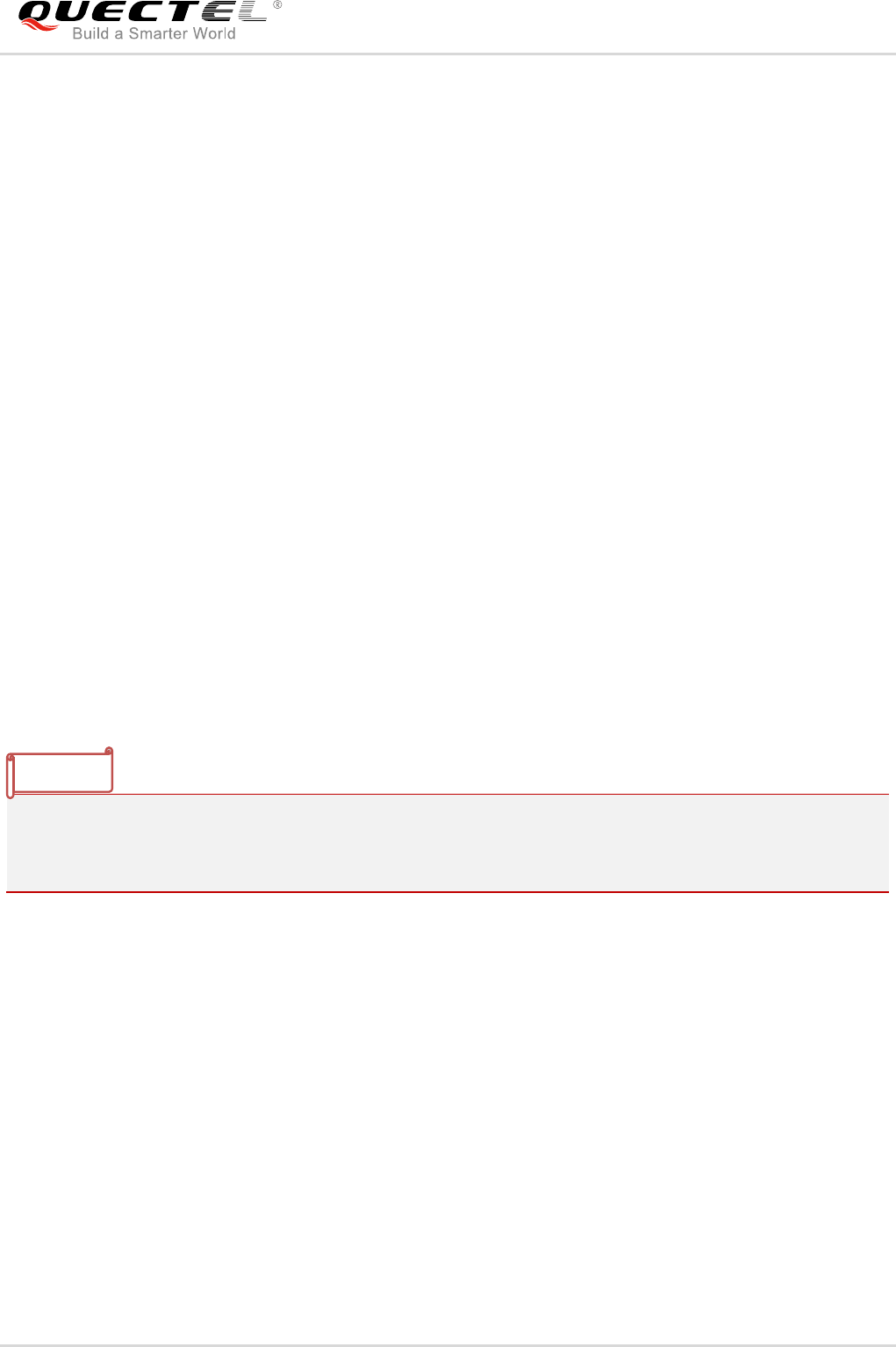
Figure 8: Recommended Stencil Design for LGA Pads
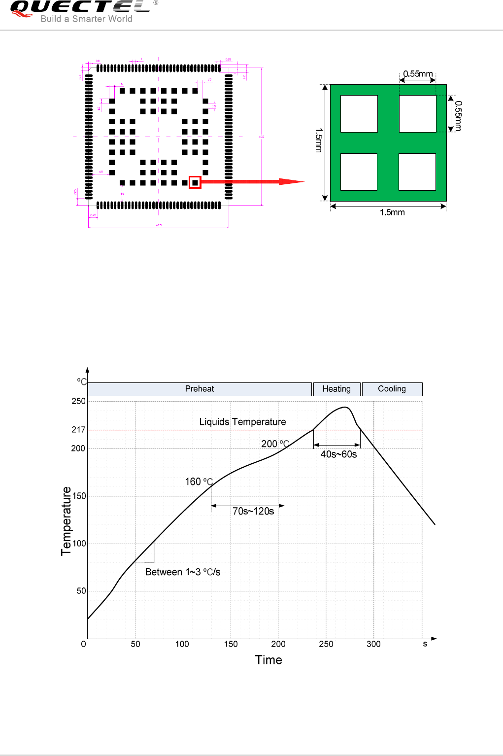
Figure 9: Reflow Soldering Thermal Profile
It is suggested that the peak reflow temperature is from 235 to 245ºC (for SnAg3.0Cu0.5 alloy). The
absolute maximum reflow temperature is 260ºC. To avoid damage to the module caused by repeated
heating, it is suggested that the module should be mounted after reflow soldering for the other side of
PCB has been completed. Recommended reflow soldering thermal profile is shown below:
SC20-A_Manual_R1.0 Confidential / Released 41 / 49
9.3. Packaging
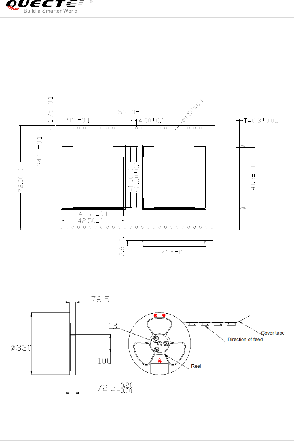
Figure 10: Tape Dimensions
Figure 11: Reel Dimensions
SC20 is packaged in tape and reel carriers. One reel is 12.32 meters long and contains 200pcs modules.
The following figures show the package details, measured in mm.

SC20-A_Manual_R1.0 Confidential / Released 42 / 49
Table 22: Reel Packaging
Model
Name MOQ for MP Minimum Package: 200pcs Minimum Package×4=800pcs
SC20 200
Size: 370mm*350mm*85mm
N.W: 1.92kg
G.W: 3.17kg
Size: 380mm*365mm*365mm
N.W:7.68 kg
G.W:13.63 kg
SC20-A_Manual_R1.0 Confidential / Released 43 / 49
10
Appendix A GPRS Coding Schemes
Table 23: Description of Different Coding Schemes
Scheme CS-1 CS-2 CS-3 C4-4
Code Rate 1/2 2/3 3/4 1
USF 3 3 3 3
Pre-coded USF 3 6 6 12
Radio Block excl.USF and BCS
181 268 312 428
BCS 40 16 16 16
Tail 4 4 4 -
Coded Bits 456 588 676 456
Punctured Bits 0 132 220 -
Data Rate Kb/s 9.05 13.4 15.6 21.4

SC20-A_Manual_R1.0 Confidential / Released 44 / 49
11
Appendix B GPRS Multi-slot Classes
3. Table 24: GPRS Multi-slot Classes
Multislot Class Downlink Slots Uplink Slots Active Slots
1 1 1 2
2 2 1 3
3 2 2 3
4 3 1 4
5 2 2 4
6 3 2 4
7 3 3 4
8 4 1 5
9 3 2 5
10 4 2 5
11 4 3 5
12 4 4 5
Twenty-nine classes of GPRS multi-slot modes are defined for MS in GPRS specification. Multi-slot
classes are product dependent, and determine the maximum achievable data rates in both the uplink and
downlink directions. Written as 3+1 or 2+2, the first number indicates the amount of downlink timeslots,
while the second number indicates the amount of uplink timeslots. The active slots determine the total
number of slots the GPRS device can use simultaneously for both uplink and downlink communications.
The description of different multi-slot classes is shown in the following table.

SC20-A_Manual_R1.0 Confidential / Released 45 / 49
12
Appendix C EDGE Modulation and
Coding Schemes
Table 25: EDGE Modulation and Coding Schemes
Coding Scheme
Modulation Coding Family 1 Timeslot 2 Timeslot 4 Timeslot
CS-1 GMSK / 9.05kbps 18.1kbps 36.2kbps
CS-2 GMSK / 13.4kbps 26.8kbps 53.6kbps
CS-3 GMSK / 15.6kbps 31.2kbps 62.4kbps
CS-4 GMSK / 21.4kbps 42.8kbps 85.6kbps
MCS-1 GMSK C 8.80kbps 17.60kbps 35.20kbps
MCS-2 GMSK B 11.2kbps 22.4kbps 44.8kbps
MCS-3 GMSK A 14.8kbps 29.6kbps 59.2kbps
MCS-4 GMSK C 17.6kbps 35.2kbps 70.4kbps
MCS-5 8-PSK B 22.4kbps 44.8kbps 89.6kbps
MCS-6 8-PSK A 29.6kbps 59.2kbps 118.4kbps
MCS-7 8-PSK B 44.8kbps 89.6kbps 179.2kbps
MCS-8 8-PSK A 54.4kbps 108.8kbps 217.6kbps
MCS-9 8-PSK A 59.2kbps 118.4kbps 236.8kbps

SC20-A_Manual_R1.0 Confidential / Released 46 / 49
13
CE Requirement
The minimum distance between the user and/or any bystander and the radiating structure of the transmitter is
20cm.
Hereby, Quectel Wireless Solutions Co., Ltd. declares that the radio equipment type SC20-E is in compliance
with Directive 2014/53/EU.
The full text of the EU declaration of conformity is available at the following internet address:
7th Floor, Hongye Building, No.1801 Hongmei Road, Xuhui District, Shanghai 200233, China
http://www.quectel.com/support/downloadb/TechnicalDocuments.htm
This SC20-E operates with the following frequency bands and maximum radio-frequency power:
GSM850/900 : 35dBm
GSM1800/1900: 32dBm
UMTS Band 1/5/8: 25 dBm
LTE Band 1/3/5/7/8/20/38/40/41: 25.7 dBm
Bluetooth:<20 dBm
WiFi 2.4GHz <20 dBm;
WiFi 5GHz band 1/2/3 <23 dBm

SC20-A_Manual_R1.0 Confidential / Released 47 / 49
14
IC & FCC Requirement
14.1. FCC Regulations:
This device complies with part 15 of the FCC Rules. Operation is subject to the following two
conditions: (1) This device may not cause harmful interference, and (2) This device must accept any
interference received, including interference that may cause undesired operation.
This device has been tested and found to comply with the limits for a Class B digital device , pursuant
to Part 15 of the FCC Rules. These limits are designed to provide reasonable protection against
harmful interference in a residential installation. This equipment generates, uses and can radiated
radio frequency energy and, if not installed and used in accordance with the instructions, may cause
harmful interference to radio communications. However, there is no guarantee that interference will
not occur in a particular installation If this equipment does cause harmful interference to radio or
television reception, which can be determined by turning the equipment off and on, the user is
encouraged to try to correct the interference by one or more of the following measures:
-Reorient or relocate the receiving antenna.
-Increase the separation between the equipment and receiver.
-Connect the equipment into an outlet on a circuit different from that to which the receiver is
connected.
-Consult the dealer or an experienced radio/TV technician for help.
Caution: Changes or modifications not expressly approved by the party responsible for compliance
could void the user‘s authority to operate the equipment.
14.2. RF Exposure Information
This device complies with FCC radiation exposure limits set forth for an uncontrolled environment. In
order to avoid the possibility of exceeding the FCC radio frequency exposure limits, human proximity
to the antenna shall not be less than 20cm (8 inches) during normal operation.
14.3. ISED Notice
This device complies with Innovation, Science and Economic Development Canada license-exempt
RSS standard(s). Operation is subject to the following two conditions:
(1) this device may not cause interference, and
(2) this device must accept any interference, including interference that may cause undesired
operation of the device.

SC20-A_Manual_R1.0 Confidential / Released 48 / 49
Le présent appareil est conforme aux CNR Innovation, Sciences et Développement économique
Canada applicables aux appareils radio exempts de licence. L'exploitation est autorisée aux deux
conditions suivantes:
(1) l'appareil ne doit pas produire de brouillage, et
(2) l'utilisateur de l'appareil doit accepter tout brouillage radioélectrique subi, même si le brouillage
est susceptible d'en
This Class B digital apparatus complies with Canadian ICES-003.
Cet appareil numérique de la classe B est conforme à la norme NMB-003 du Canada.
14.4. ISED Radiation Exposure Statement
This device complies with RSS-102 radiation exposure limits set forth for an uncontrolled
environment. In order to avoid the possibility of exceeding the ISED radio frequency exposure limits,
human proximity to the antenna shall not be less than 20cm (8 inches) during normal operation.
Cet appareil est conforme aux limites d'exposition aux rayonnements de la CNR-102 définies pour
un environnement non contrôlé. Afin d'éviter la possibilité de dépasser les limites d'exposition aux
fréquences radio de la CNR-102, la proximité humaine à l'antenne ne doit pas être inférieure à 20 cm
(8 pouces) pendant le fonctionnement normal.
14.5. IMPORTANT NOTE:
This module is intended for OEM integrator. The OEM integrator is still responsible for the FCC
compliance requirement of the end product, which integrates this module. 20cm minimum distance
has to be able to be maintained between the antenna and the users for the host this module is
integrated into. Under such configuration, the FCC radiation exposure limits set forth for an
population/uncontrolled environment can be satisfied.
Any changes or modifications not expressly approved by the manufacturer could void the user's
authority to operate this equipment.
14.6. USERS MANUAL OF THE END PRODUCT:
In the users manual of the end product, the end user has to be informed to keep at least 20cm
separation with the antenna while this end product is installed and operated. The end user has to be
informed that the FCC radio-frequency exposure guidelines for an uncontrolled environment can be
satisfied. The end user has to also be informed that any changes or modifications not expressly
approved by the manufacturer could void the user's authority to operate this equipment. If the size of
the end product is smaller than 8x10cm, then additional FCC part 15.19 statement is required to be
available in the users manual: This device complies with Part 15 of FCC rules. Operation is subject to
the following two conditions: (1) this device may not cause harmful interference and (2) this device
must accept any interference received, including interference that may cause undesired operation.

SC20-A_Manual_R1.0 Confidential / Released 49 / 49
14.7. LABEL OF THE END PRODUCT:
The final end product must be labeled in a visible area with the following " Contains Transmitter
Module FCC ID: XMR201706SC20A". If the size of the end product is larger than 8x10cm, then the
following FCC part 15.19 statement has to also be available on the label: This device complies with
Part 15 of FCC rules.
Operation is subject to the following two conditions: (1) this device may not cause harmful
interference and (2) this device must accept any interference received, including interference that
may cause undesired operation.
The Innovation, Science and Economic Development Canada certification label of a module shall be
clearly visible at all times when installed in the host device; otherwise, the host device must be
labeled to display the Innovation, Science and Economic Development Canada certification number
for the module, preceded by the words “Contains transmitter module IC: 10224A-201707SC20A”.
The device is going on be operated in 5150~5250 frequency range. It is restricted indoor
environment only in Canada.
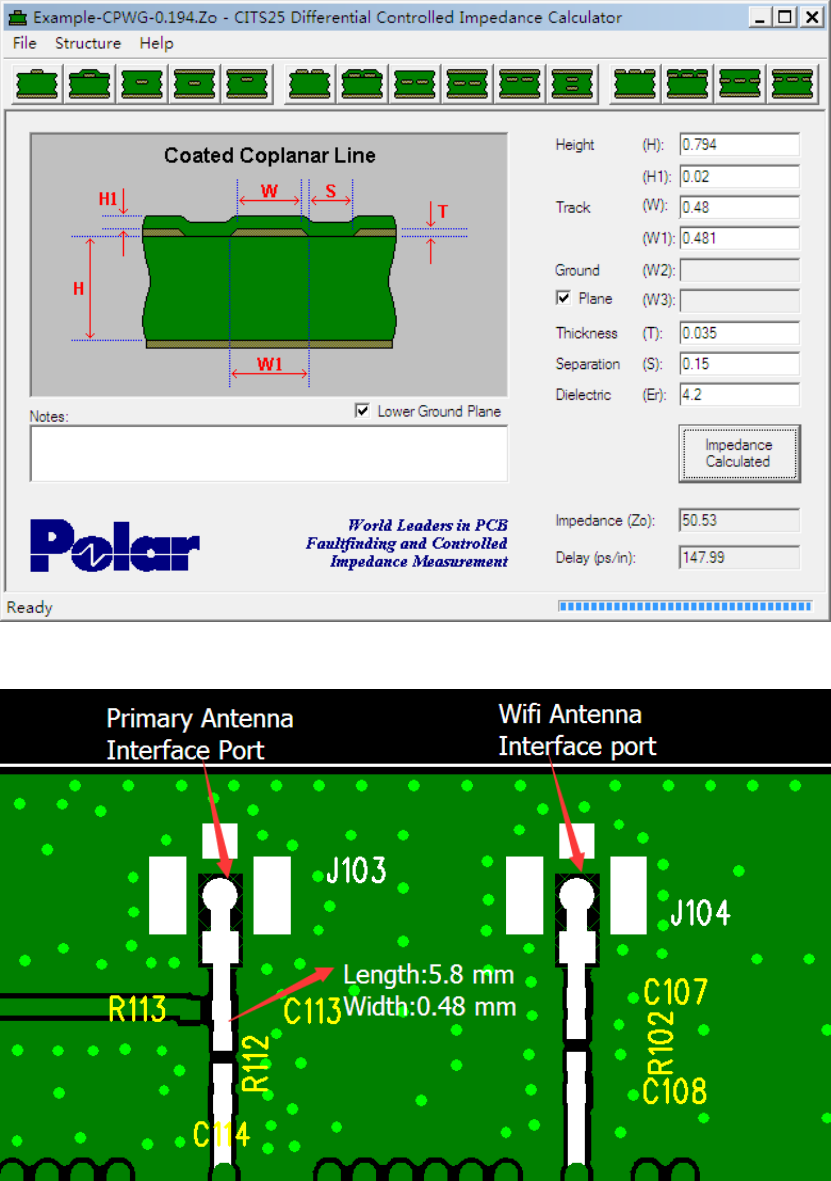
1、the characteristic impedence depends on the dielectric of PCB, the trace width and the grand
plane spacing,Coated Coplanar Line is required.the detail simulation as below.
2、the RF trace of the test board which was used in the FCC test is defined as below.
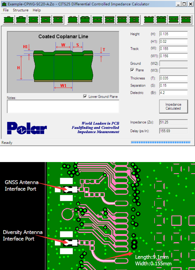
3、the characteristic impedence depends on the dielectric of PCB, the trace width and the grand
plane spacing,Coated Coplanar Line is required.the detail simulation as below.
4、the RF trace of the test board which was used in the FCC test is defined as below.