Quectel Wireless Solutions 201707BG96 Quectel BG96 User Manual
Quectel Wireless Solutions Company Limited Quectel BG96 Users Manual
UserManual.wiki
>
Quectel Wireless Solutions
>
201707BG96 User Manual
>
Users Manual
Contents
1.
Users Manual
2.
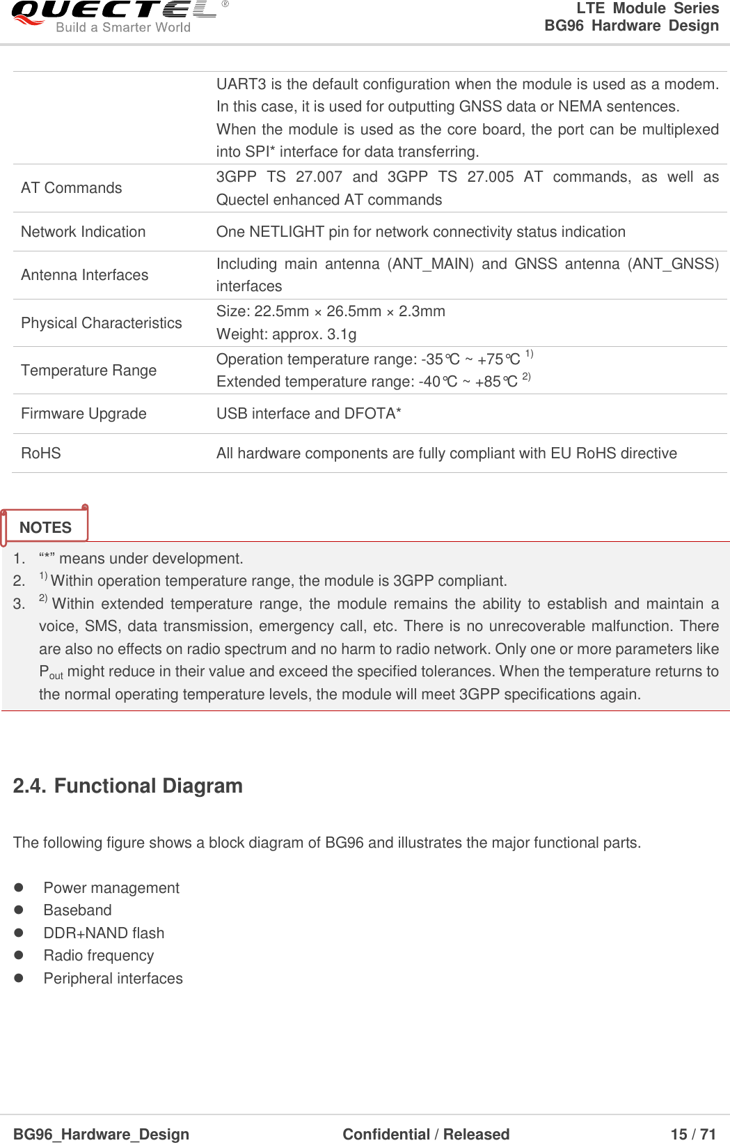
User manual
Users Manual
Navigation menu
Upload a User Manual
Namespaces
Wiki Guide
HTML
PDF
Info
Views
User Manual
Discussion / Help
Navigation
![LTE Module Series BG96 Hardware Design BG96_Hardware_Design Confidential / Released 29 / 71 Switching on the power switch to supply power to USB_VBUS will wake up the module. 1. Please pay attention to the level match shown in dotted line between the module and the host. Refer to document [1] for more details about BG96 power management application. 2. “*” means under development. 3.4.2. Airplane Mode When the module enters into airplane mode, the RF function does not work, and all AT commands correlative with RF function will be inaccessible. This mode can be set via the following ways. Hardware: W_DISABLE# is pulled up by default. Driving it to low level will let the module enter into airplane mode. Software: AT+CFUN=<fun> command provides choice of the functionality level, through setting <fun> into 0, 1 or 4. AT+CFUN=0: Minimum functionality mode. Both (U)SIM and RF functions are disabled. AT+CFUN=1: Full functionality mode (by default). AT+CFUN=4: Airplane mode. RF function is disabled. 1. Airplane mode control via W_DISABLE# is disabled in firmware by default. It can be enabled by AT+QCFG=“airplanecontrol” command. The command is still under development. 2. The execution of AT+CFUN command will not affect GNSS function. 3.5. Power Supply 3.5.1. Power Supply Pins BG96 provides four VBAT pins for connection with an external power supply. There are two separate voltage domains for VBAT. Two VBAT_RF pins for module’s RF part. Two VBAT_BB pins for module’s baseband part. The following table shows the details of VBAT pins and ground pins. NOTES NOTES](https://usermanual.wiki/Quectel-Wireless-Solutions/201707BG96.Users-Manual/User-Guide-3470700-Page-30.png)
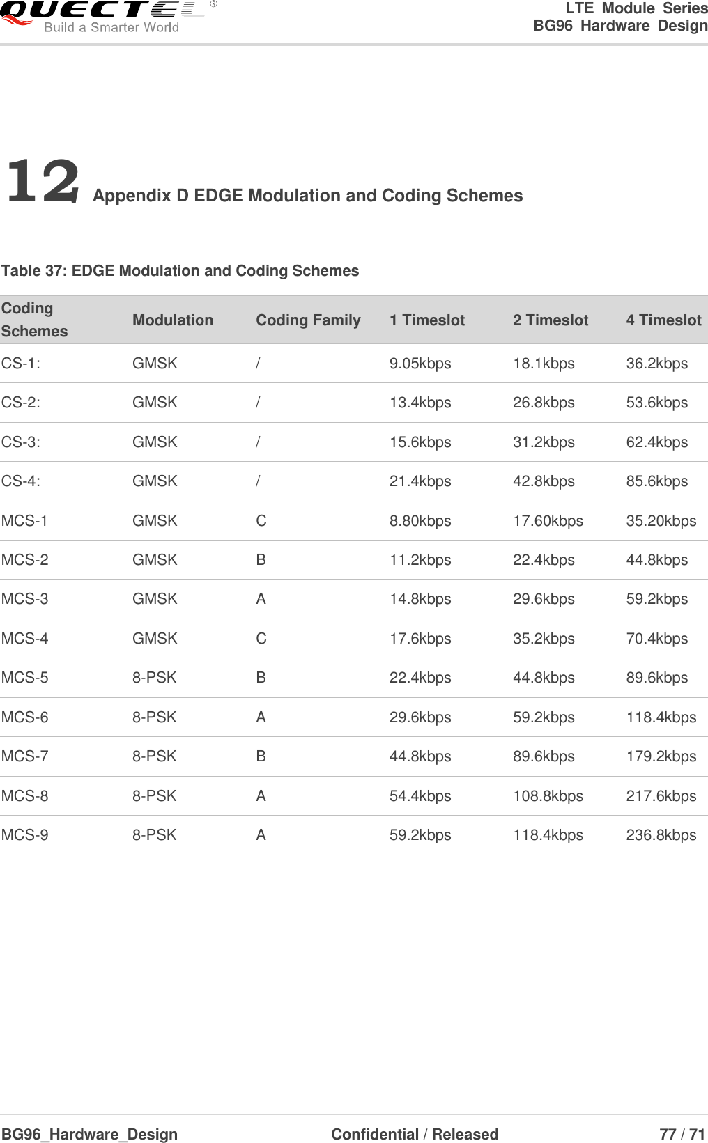
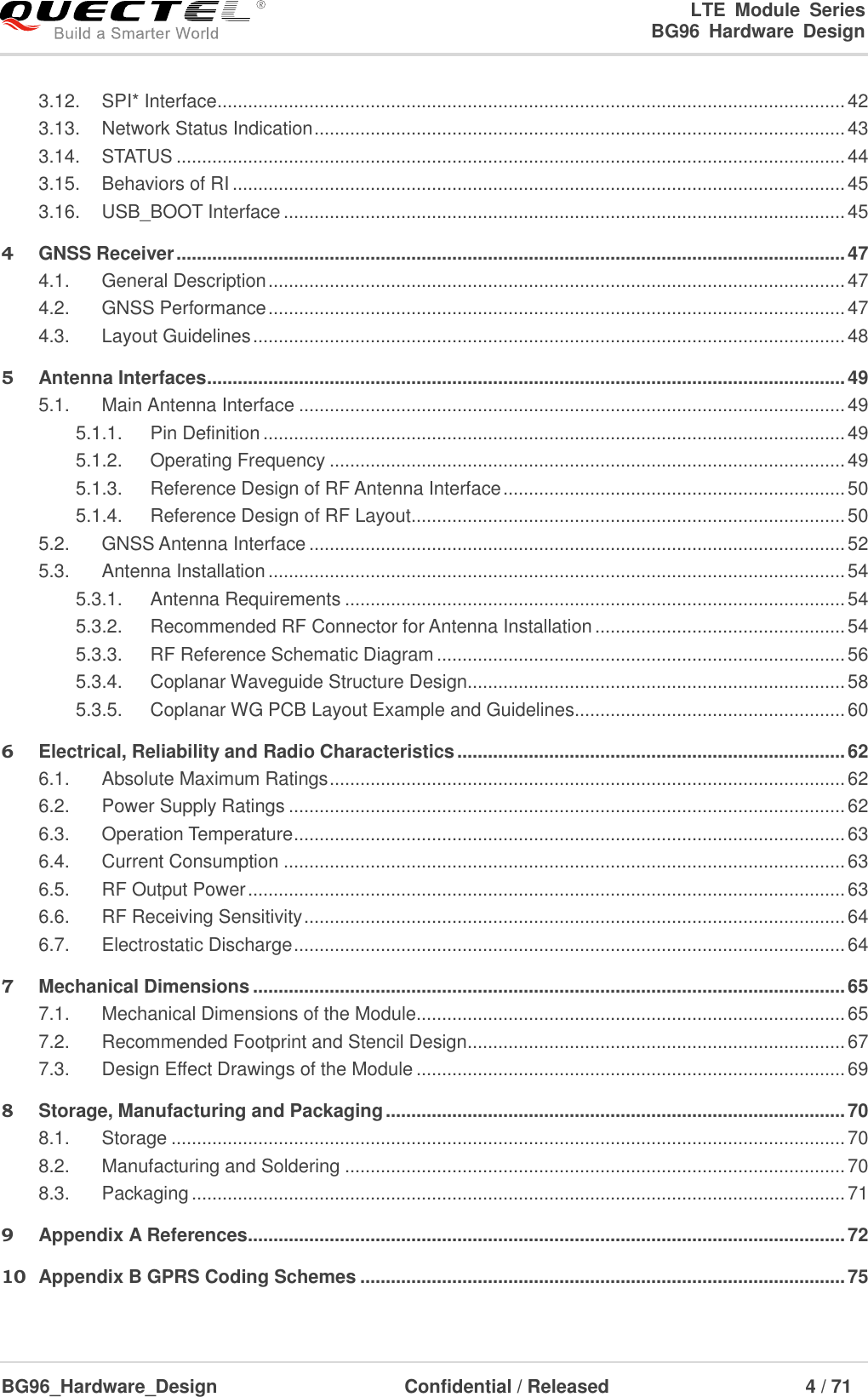
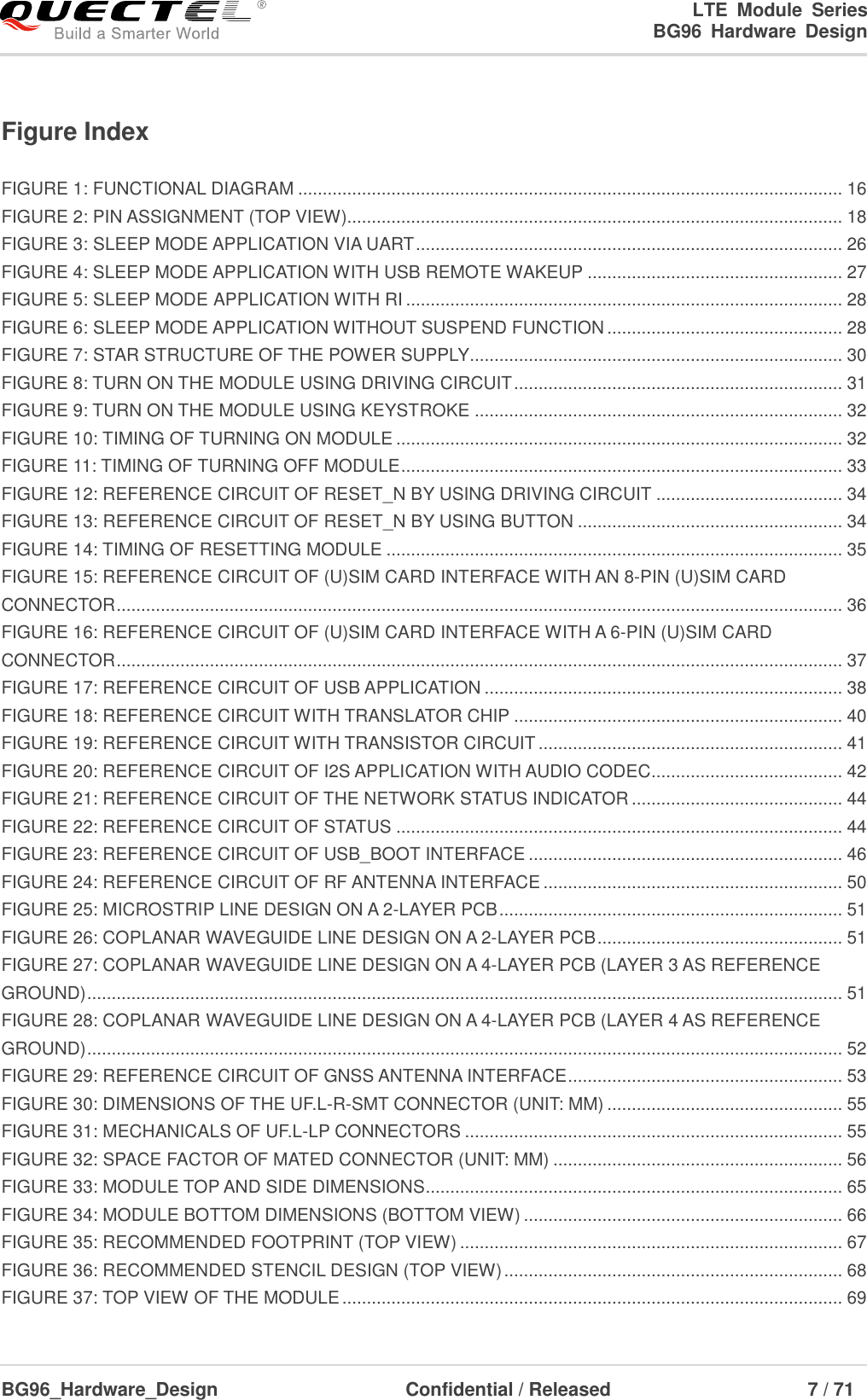
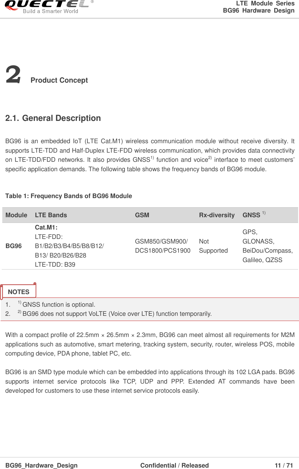
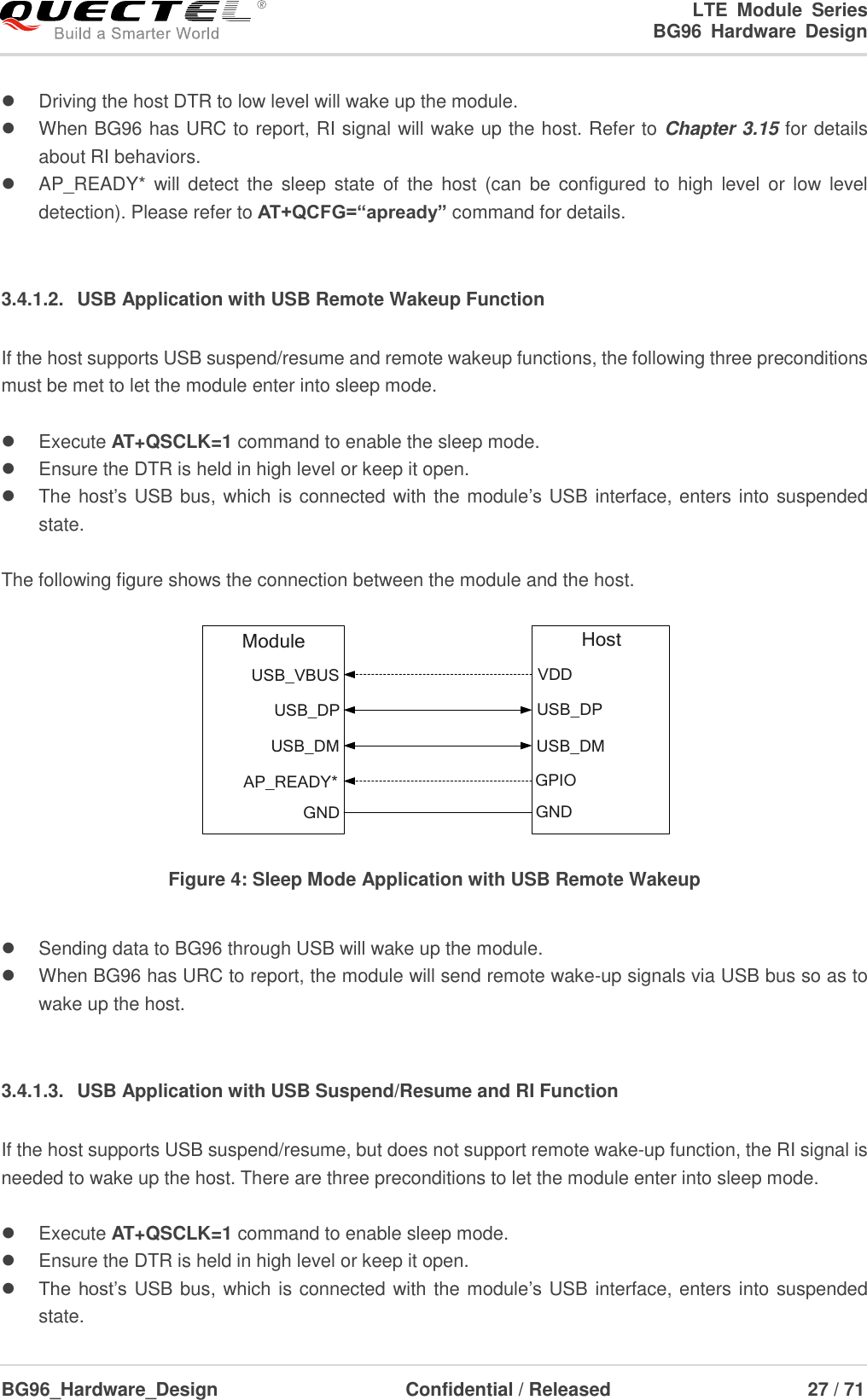
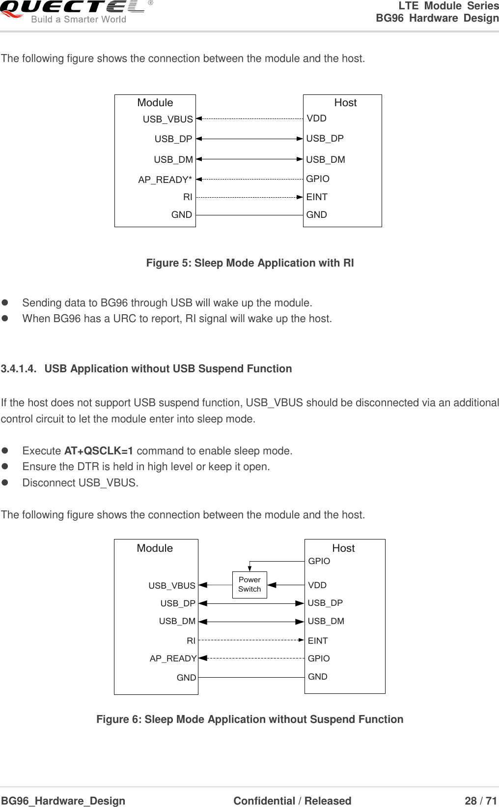
![LTE Module Series BG96 Hardware Design BG96_Hardware_Design Confidential / Released 31 / 71 3.5.3. Monitor the Power Supply AT+CBC command can be used to monitor the VBAT_BB voltage value. For more details, please refer to document [2]. 3.6. Turn on and off Scenarios 3.6.1. Turn on Module Using the PWRKEY Pin The following table shows the pin definition of PWRKEY. Table 7: Pin Definition of PWRKEY Pin Name Pin No. Description DC Characteristics Comment PWRKEY 15 Turn on/off the module VIHmax=2.1V VIHmin=1.3V VILmax=0.5V The output voltage is 0.8V because of the diode drop in the Qualcomm chipset. When BG96 is in power down mode, it can be turned on to normal mode by driving the PWRKEY pin to a low level for at least 100ms. It is recommended to use an open drain/collector driver to control the PWRKEY. After STATUS pin (require external pull-up) outputting a low level, PWRKEY pin can be released. A simple reference circuit is illustrated in the following figure. Turn on pulsePWRKEY4.7K47K≥100ms Figure 8: Turn on the Module Using Driving Circuit The other way to control the PWRKEY is using a button directly. When pressing the key, electrostatic strike may generate from finger. Therefore, a TVS component is indispensable to be placed nearby the button for ESD protection. A reference circuit is shown in the following figure.](https://usermanual.wiki/Quectel-Wireless-Solutions/201707BG96.Users-Manual/User-Guide-3470700-Page-32.png)
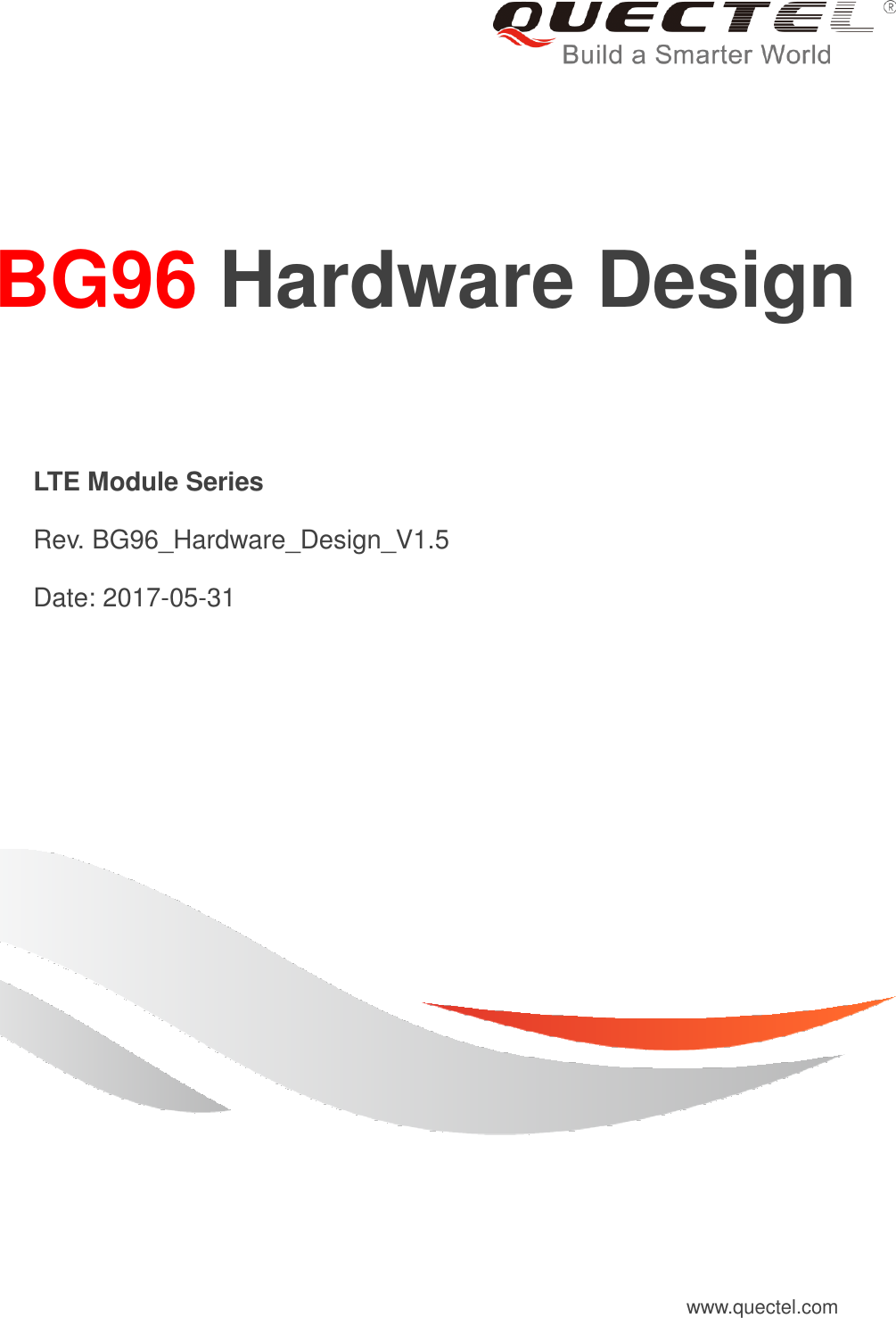
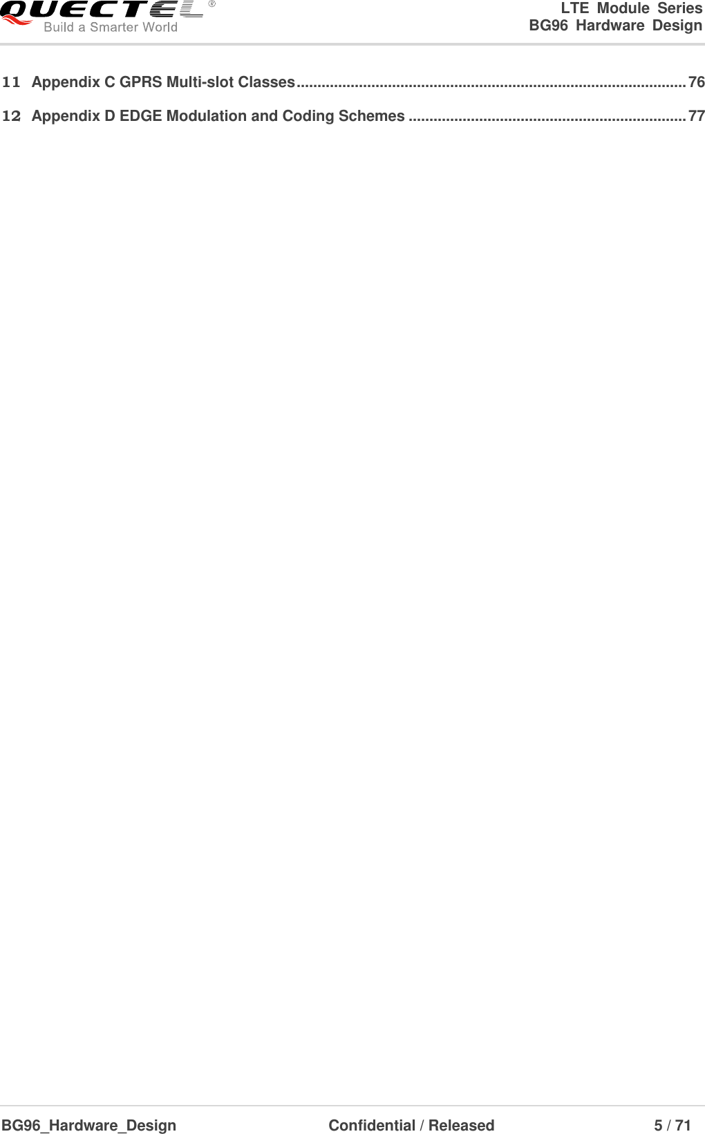
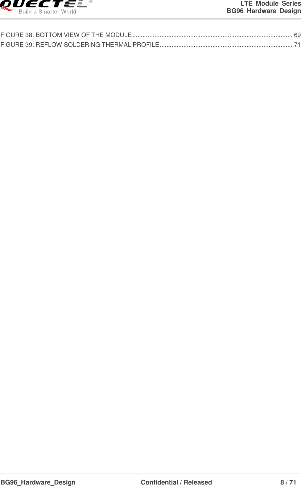
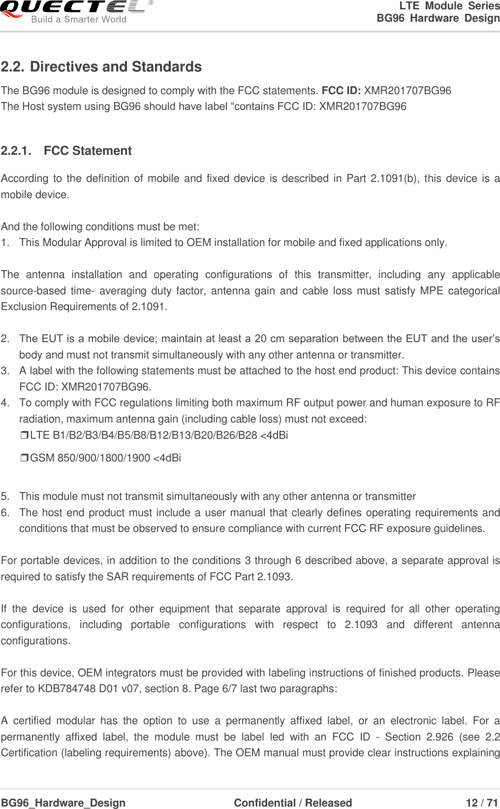
![LTE Module Series BG96 Hardware Design BG96_Hardware_Design Confidential / Released 33 / 71 3.6.2. Turn off Module The following procedures can be used to turn off the module: Normal power down procedure: Turn off the module using the PWRKEY pin. Normal power down procedure: Turn off the module using AT+QPOWD command. 3.6.2.1. Turn off Module Using the PWRKEY Pin Driving the PWRKEY pin to a low level voltage (the specific time is TBD), the module will execute power-down procedure after the PWRKEY is released. The power-down scenario is illustrated in the following figure. VBATPWRKEYTBDTBDRUNNING Power-down procedure OFFModuleStatusSTATUS Figure 11: Timing of Turning off Module 3.6.2.2. Turn off Module Using AT Command It is also a safe way to use AT+QPOWD command to turn off the module, which is similar to turning off the module via PWRKEY pin. Please refer to document [2] for details about AT+QPOWD command.](https://usermanual.wiki/Quectel-Wireless-Solutions/201707BG96.Users-Manual/User-Guide-3470700-Page-34.png)
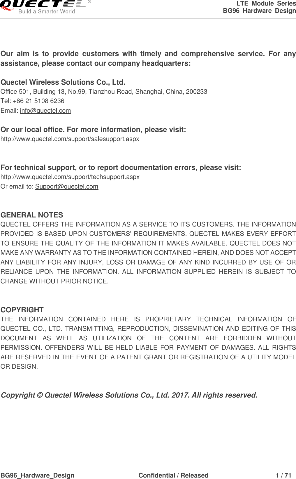
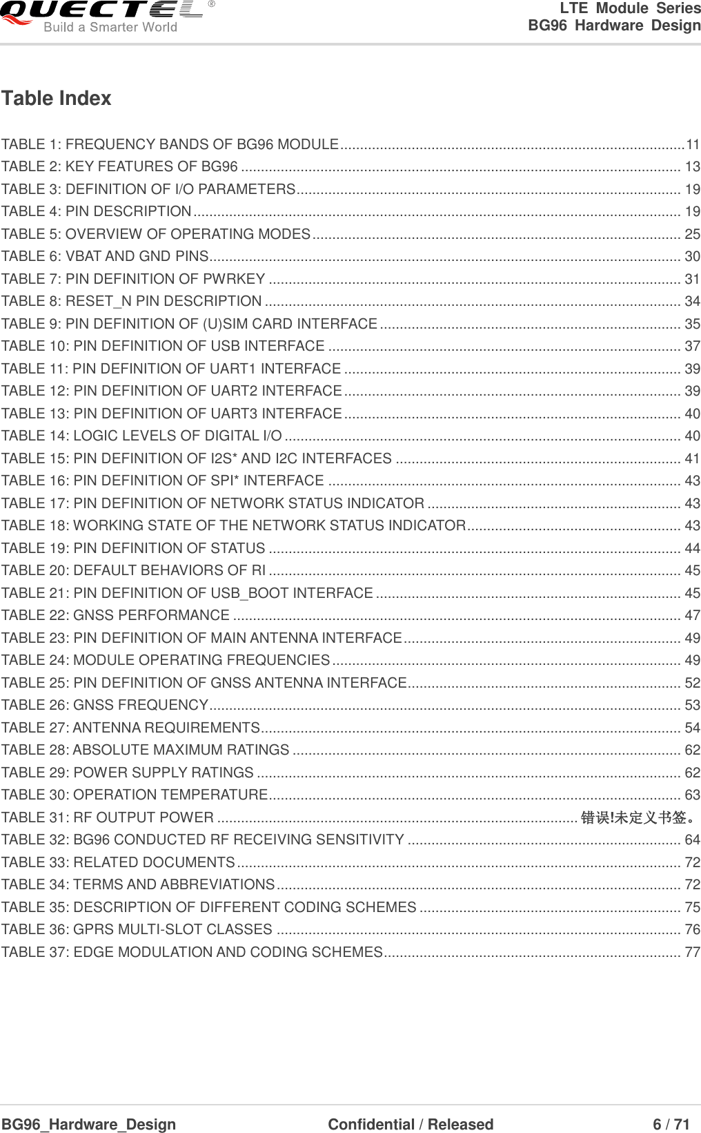
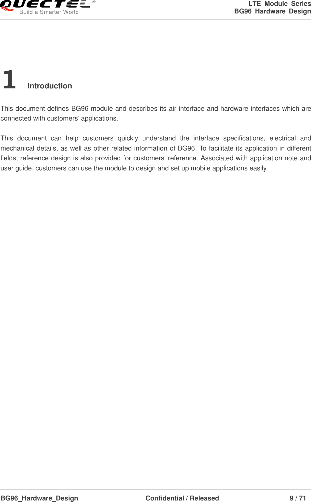
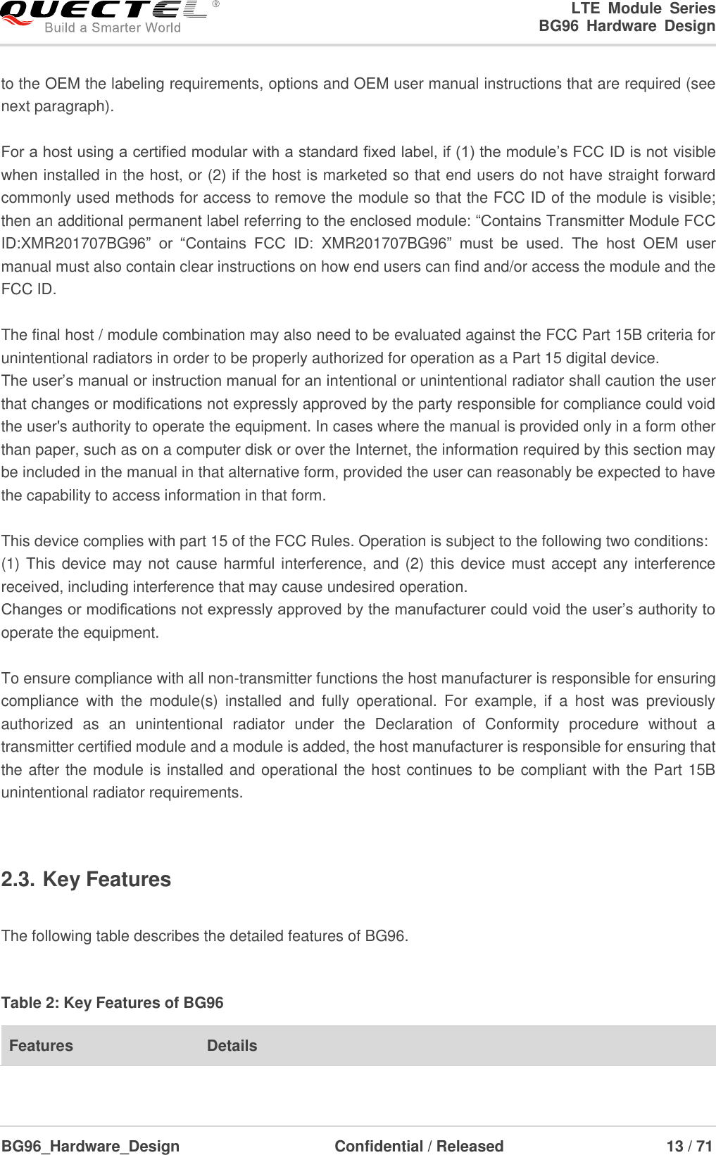
![LTE Module Series BG96 Hardware Design BG96_Hardware_Design Confidential / Released 36 / 71 BG96 supports (U)SIM card hot-plug via the USIM_PRESENCE pin. The function supports low level and high level detections, and is disabled by default. Please refer to document [2] about AT+QSIMDET command for details. The following figure shows a reference design of (U)SIM card interface with an 8-pin (U)SIM card connector. ModuleUSIM_VDDUSIM_GNDUSIM_RSTUSIM_CLKUSIM_DATAUSIM_PRESENCE22R22R22RVDD_EXT51K100nF (U)SIM Card ConnectorGNDGND33pF 33pF 33pFVCCRSTCLK IOVPPGNDGNDUSIM_VDD15K Figure 15: Reference Circuit of (U)SIM Card Interface with an 8-Pin (U)SIM Card Connector If (U)SIM card detection function is not needed, please keep USIM_PRESENCE unconnected. A reference circuit for (U)SIM card interface with a 6-pin (U)SIM card connector is illustrated in the following figure. ModuleUSIM_VDDUSIM_GNDUSIM_RSTUSIM_CLKUSIM_DATA 22R22R22R100nF (U)SIM Card ConnectorGND33pF 33pF 33pFVCCRSTCLK IOVPPGNDGND15KUSIM_VDD](https://usermanual.wiki/Quectel-Wireless-Solutions/201707BG96.Users-Manual/User-Guide-3470700-Page-37.png)
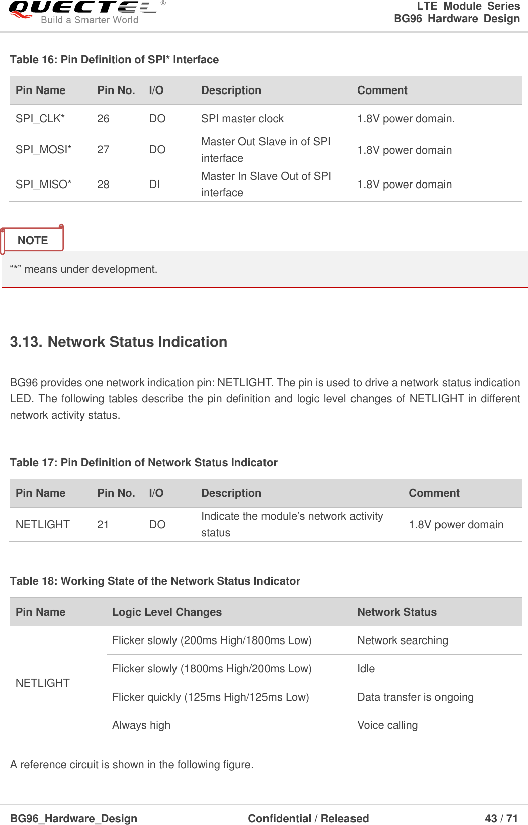
![LTE Module Series BG96 Hardware Design BG96_Hardware_Design Confidential / Released 45 / 71 3.15. Behaviors of RI AT+QCFG=“risignaltype”,“physical” command can be used to configure RI behavior. No matter on which port URC is presented, URC will trigger the behavior of RI pin. URC can be outputted from UART port, USB AT port and USB modem port, through configuration via AT+QURCCFG command. The default port is USB AT port. The default behaviors of RI are shown as below. Table 20: Default Behaviors of RI State Response Idle RI keeps in high level. URC RI outputs 120ms low pulse when new URC returns. The default RI behaviors can be configured flexibly by AT+QCFG=“urc/ri/ring” command. AT+QCFG command is still under development. For more details, please refer to document [2]. 3.16. USB_BOOT Interface BG96 provides a USB_BOOT pin. During development or factory production, USB_BOOT pin can force the module to boot from USB port for firmware upgrade. Table 21: Pin Definition of USB_BOOT Interface Pin Name Pin No. I/O Description Comment USB_BOOT 75 DI Force the module to boot from USB port 1.8V power domain. Active high. If unused, keep it open. NOTE](https://usermanual.wiki/Quectel-Wireless-Solutions/201707BG96.Users-Manual/User-Guide-3470700-Page-46.png)
![LTE Module Series BG96 Hardware Design BG96_Hardware_Design Confidential / Released 47 / 71 4 GNSS Receiver 4.1. General Description BG96 includes a fully integrated global navigation satellite system solution that supports Gen8C-Lite of Qualcomm (GPS, GLONASS, BeiDou/Compass, Galileo and QZSS). BG96 supports standard NMEA-0183 protocol, and outputs NMEA sentences at 1Hz data update rate via USB interface by default. By default, BG96 GNSS engine is switched off. It has to be switched on via AT command. For more details about GNSS engine technology and configurations, please refer to document [3]. 4.2. GNSS Performance The following table shows the GNSS performance of BG96. Table 22: GNSS Performance Parameter Description Conditions Typ. Unit Sensitivity (GNSS) Cold start Autonomous TBD dBm Reacquisition Autonomous TBD dBm Tracking Autonomous TBD dBm TTFF (GNSS) Cold start @open sky Autonomous TBD s XTRA* enabled TBD s Warm start @open sky Autonomous TBD s XTRA* enabled TBD s Hot start Autonomous TBD s](https://usermanual.wiki/Quectel-Wireless-Solutions/201707BG96.Users-Manual/User-Guide-3470700-Page-48.png)
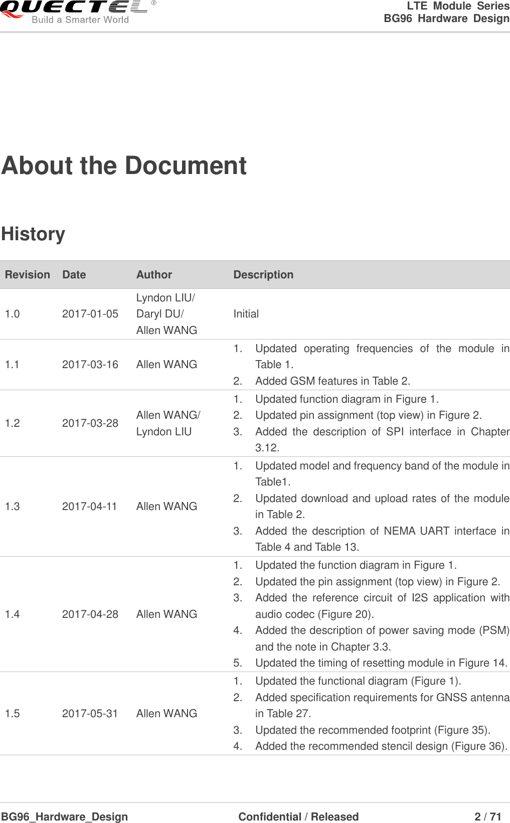
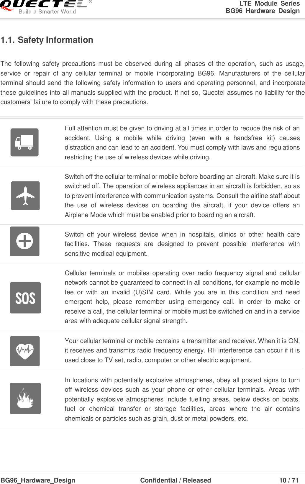
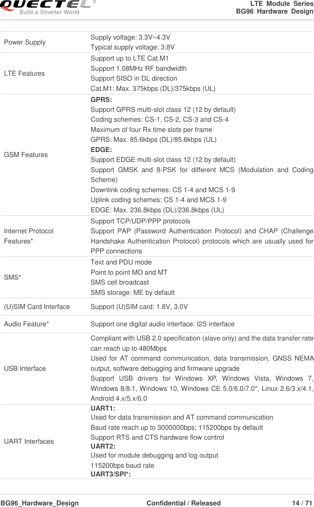
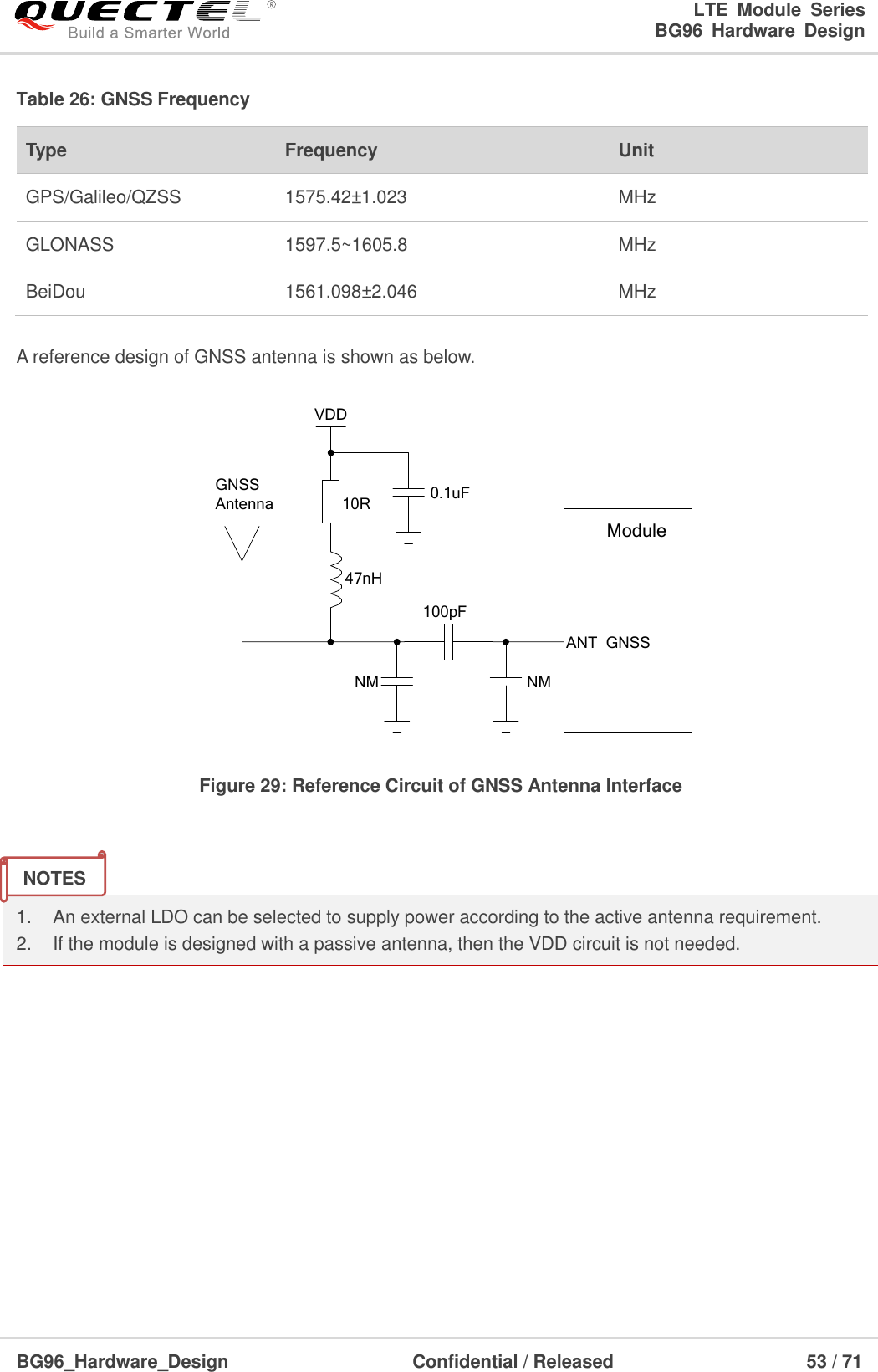
![LTE Module Series BG96 Hardware Design BG96_Hardware_Design Confidential / Released 52 / 71 Figure 28: Coplanar Waveguide Line Design on a 4-layer PCB (Layer 4 as Reference Ground) In order to ensure RF performance and reliability, the following principles should be complied with in RF layout design: Use impedance simulation tool to control the characteristic impedance of RF traces as 50Ω. The GND pins adjacent to RF pins should not be hot welded, and should be fully connected to ground. The distance between the RF pins and the RF connector should be as short as possible, and all the right angle traces should be changed to curved ones. There should be clearance area under the signal pin of the antenna connector or solder joint. The reference ground of RF traces should be complete. Meanwhile, adding some ground vias around RF traces and the reference ground could help to improve RF performance. The distance between the ground vias and RF traces should be no less than two times the width of RF signal traces (2*W). For more details about RF layout, please refer to document [4]. 5.2. GNSS Antenna Interface The following tables show the pin definition and frequency specification of GNSS antenna interface. Table 25: Pin Definition of GNSS Antenna Interface Pin Name Pin No. I/O Description Comment ANT_GNSS 49 AI GNSS antenna interface 50Ω impedance](https://usermanual.wiki/Quectel-Wireless-Solutions/201707BG96.Users-Manual/User-Guide-3470700-Page-53.png)
![LTE Module Series BG96 Hardware Design BG96_Hardware_Design Confidential / Released 70 / 71 8 Storage, Manufacturing and Packaging 8.1. Storage BG96 is stored in a vacuum-sealed bag. The storage restrictions are shown as below. 1. Shelf life in the vacuum-sealed bag: 12 months at <40ºC/90%RH. 2. After the vacuum-sealed bag is opened, devices that will be subjected to reflow soldering or other high temperature processes must be: Mounted within 168 hours at the factory environment of ≤30ºC/60%RH. Stored at <10%RH. 3. Devices require baking before mounting, if any circumstance below occurs. When the ambient temperature is 23ºC±5ºC and the humidity indication card shows the humidity is >10% before opening the vacuum-sealed bag. Device mounting cannot be finished within 168 hours at factory conditions of ≤30ºC/60% 4. If baking is required, devices may be baked for 48 hours at 125ºC±5ºC. As the plastic package cannot be subjected to high temperature, it should be removed from devices before high temperature (125ºC ) baking. If shorter baking time is desired, please refer to IPC/JEDECJ-STD-033 for baking procedure. 8.2. Manufacturing and Soldering Push the squeegee to apply the solder paste on the surface of stencil, thus making the paste fill the stencil openings and then penetrate to the PCB. The force on the squeegee should be adjusted properly so as to produce a clean stencil surface on a single pass. To ensure the module soldering quality, the thickness of stencil for the module is recommended to be 0.18mm. For more details, please refer to document [5]. NOTE](https://usermanual.wiki/Quectel-Wireless-Solutions/201707BG96.Users-Manual/User-Guide-3470700-Page-71.png)
![LTE Module Series BG96 Hardware Design BG96_Hardware_Design Confidential / Released 72 / 71 9 Appendix A References Table 33: Related Documents SN Document Name Remark [1] Quectel_BG96_Power_Management_Application_Note BG96 Power Management Application Note [2] Quectel_BG96_AT_Commands_Manual BG96 AT Commands Manual [3] Quectel_BG96_GNSS_AT_Commands_Manual BG96 GNSS AT Commands Manual [4] Quectel_RF_Layout_Application_Note RF Layout Application Note [5] Quectel_Module_Secondary_SMT_User_Guide Module Secondary SMT User Guide Table 34: Terms and Abbreviations Abbreviation Description AMR Adaptive Multi-rate bps Bits Per Second CHAP Challenge Handshake Authentication Protocol CS Coding Scheme CTS Clear To Send DC-HSPA+ Dual-carrier High Speed Packet Access DFOTA Delta Firmware Upgrade Over The Air DL Downlink DTR Data Terminal Ready DTX Discontinuous Transmission EFR Enhanced Full Rate](https://usermanual.wiki/Quectel-Wireless-Solutions/201707BG96.Users-Manual/User-Guide-3470700-Page-73.png)