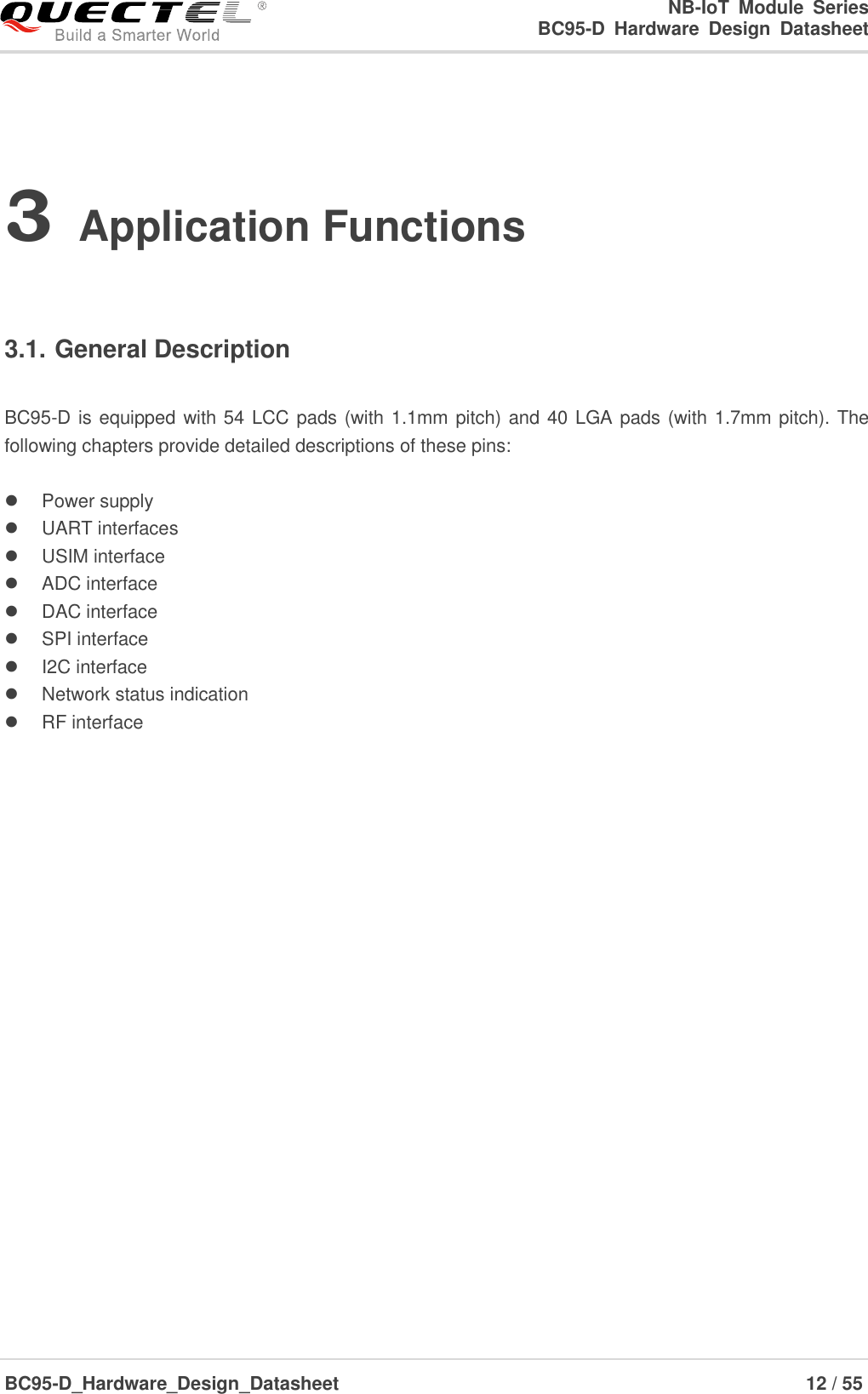
Quectel Wireless Solutions 201807BC95D NB-IoT Module User Manual
Quectel Wireless Solutions Company Limited NB-IoT Module Users Manual
UserManual.wiki
>
Quectel Wireless Solutions
>
201807BC95D User Manual
Users Manual
Navigation menu
Upload a User Manual
Namespaces
Wiki Guide
HTML
PDF
Info
Views
User Manual
Discussion / Help
Navigation
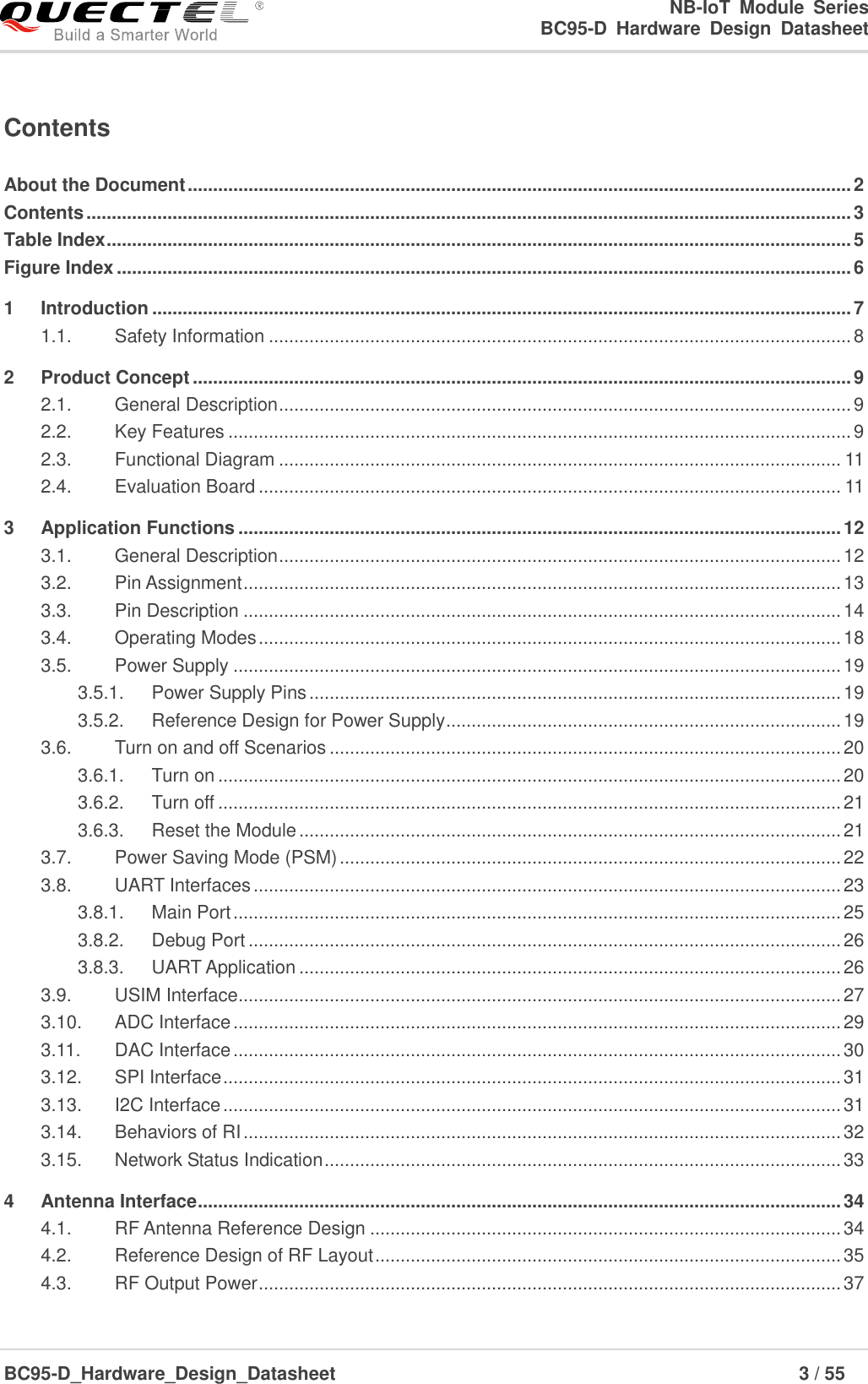

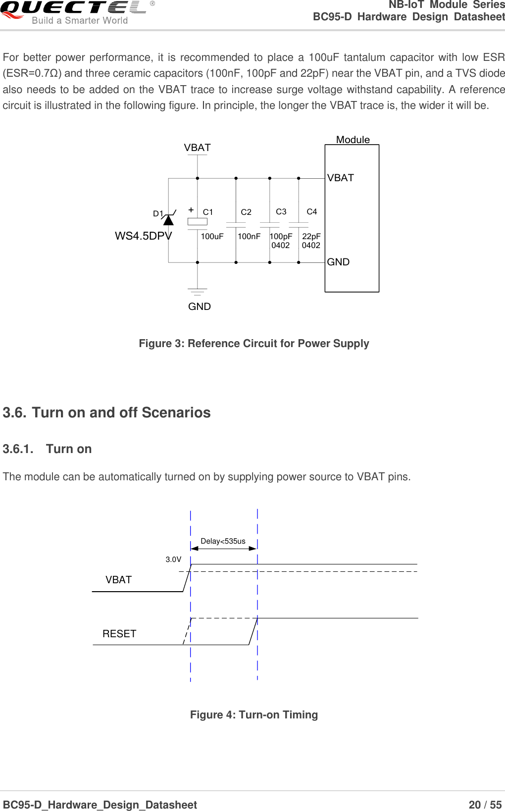
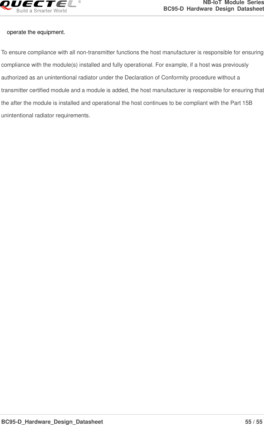
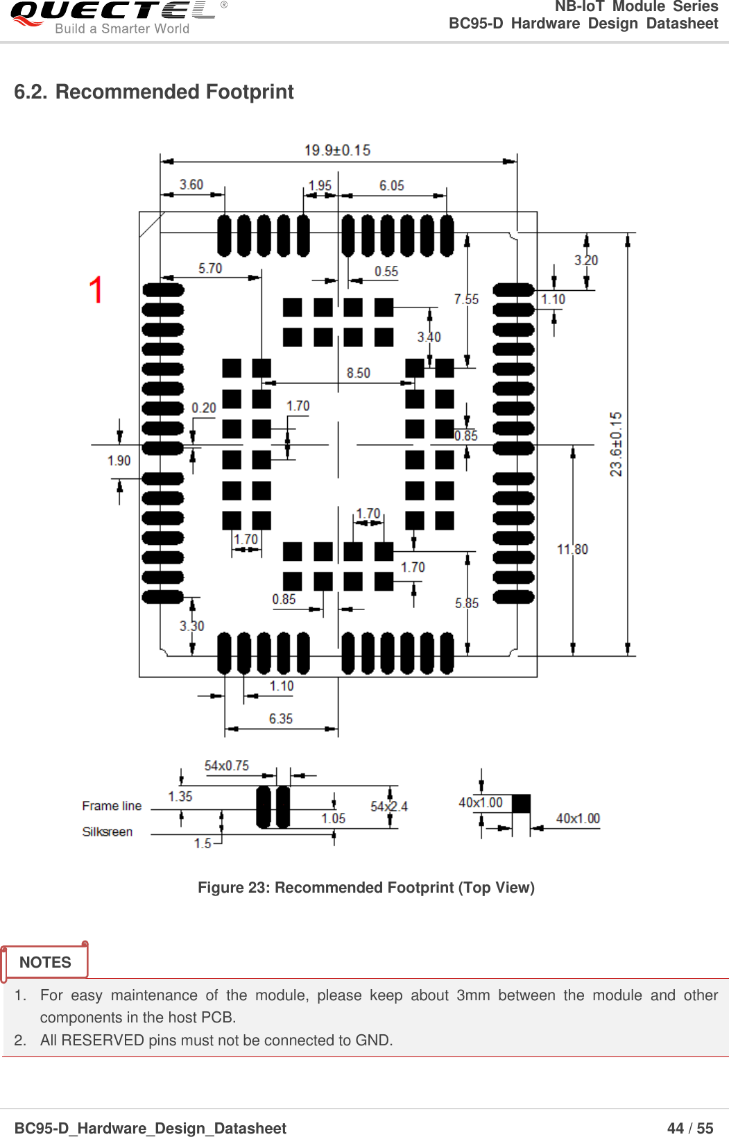
![NB-IoT Module Series BC95-D Hardware Design Datasheet BC95-D_Hardware_Design_Datasheet 21 / 55 3.6.2. Turn off The module can be turned off by shutting down the VBAT power supply. VBATRESETDelay>5ms3.0V Figure 5: Turn-off Timing 3.6.3. Reset the Module The module can be reset by the following two ways. The reset timing is illustrated as the following table. Hardware Reset the module by driving the reset pin to a low level voltage for more than 100ms. Software Reset the module using command AT+NRB. For more details about the command, please refer to document [1]. Table 7: Reset Characteristics The recommended circuits of hardware resetting are shown as below. An open drain/collector driver or button can be used to control the RESET pin. Pin Name Pin No. Description Reset Pull-down Time RESET 15 Reset the module. Active low >100ms](https://usermanual.wiki/Quectel-Wireless-Solutions/201807BC95D/User-Guide-3924973-Page-22.png)
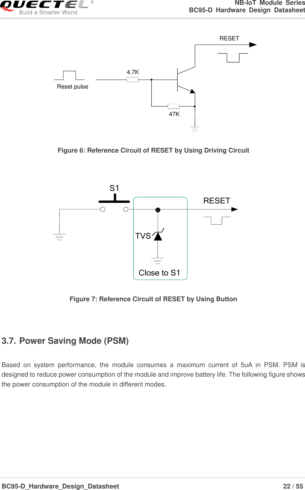
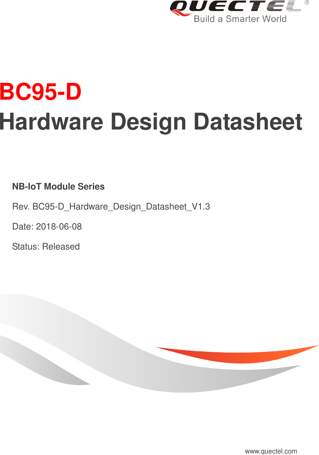
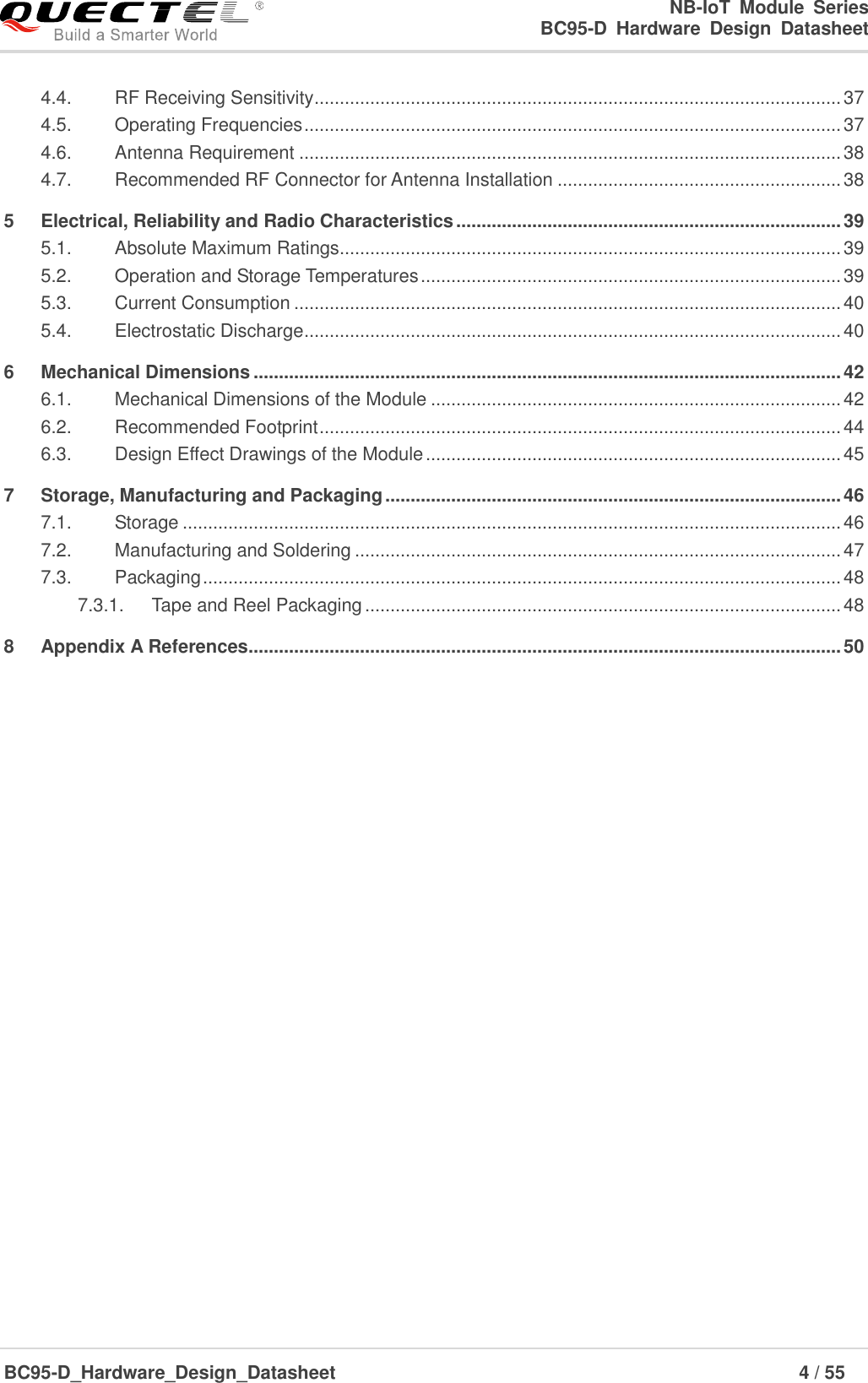
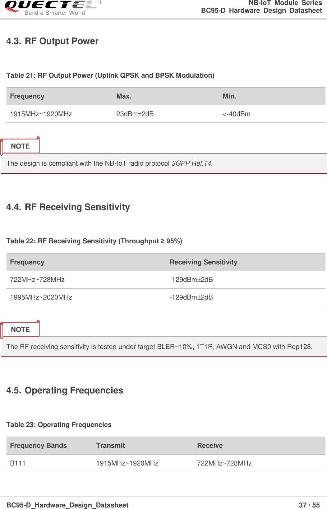
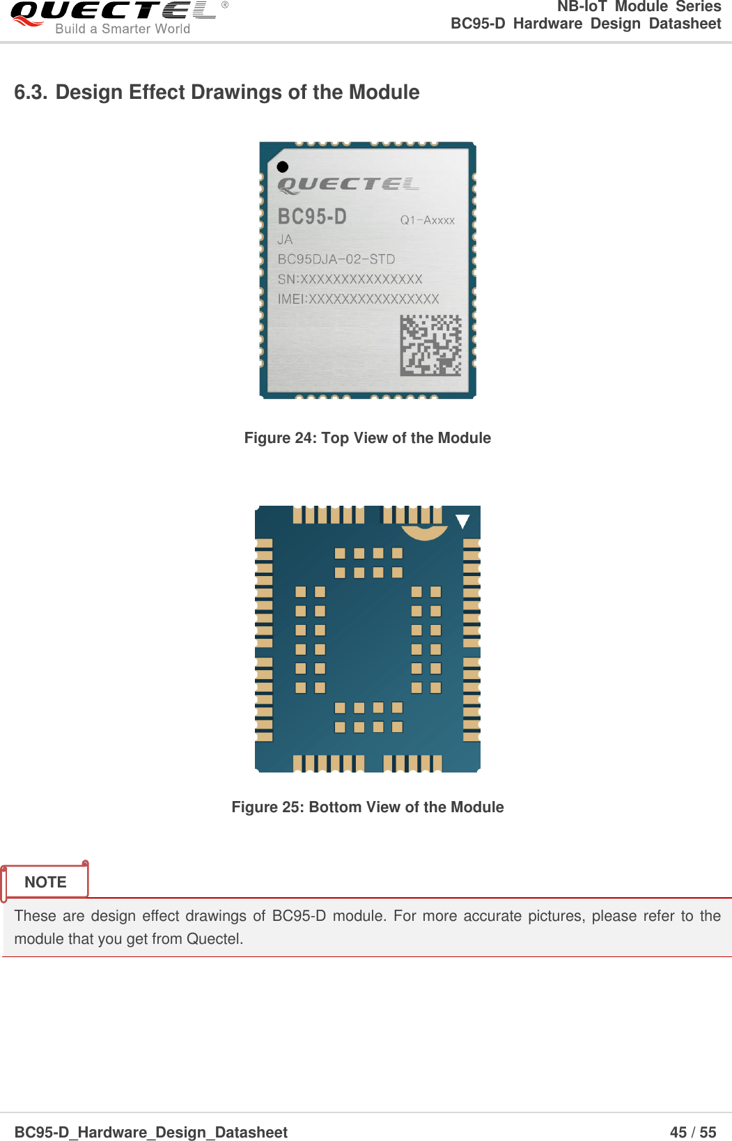
![NB-IoT Module Series BC95-D Hardware Design Datasheet BC95-D_Hardware_Design_Datasheet 25 / 55 Table 10: UART and LPUART Settings 1. “*” means under development. 2. 1) 1Mbps baud rate should always be supported, and a higher baud rate can be configured according to actual needs. 3.8.1. Main Port The main port can be used for AT command communication and data transmission, and in such case the baud rate supports 4800bps, 9600bps and 115200bps, and the default baud rate is 9600bps. It can also be used for firmware upgrading and in such case the baud rate is 921600bps. This main port is available in active mode, idle mode and PSM. For more information about firmware upgrading, please refer to document [2]. The following figure shows the connection between the DCE and DTE. TXDRXDRITXDRXDRINGModule (DCE)Serial portMain portGND GNDPC (DTE) Figure 9: Reference Design for Main Port Parameter Supported Value UART Baud Rate 45.8bps to 3Mbps1) LPUART Baud Rate 128bps to 57600bps Parity Even/Odd/None Number of Stop Bits 1 or 2 bits Data Bits Per Frame 5, 6, 7 or 8 bits NOTES](https://usermanual.wiki/Quectel-Wireless-Solutions/201807BC95D/User-Guide-3924973-Page-26.png)
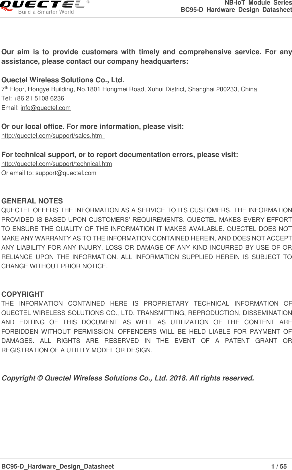
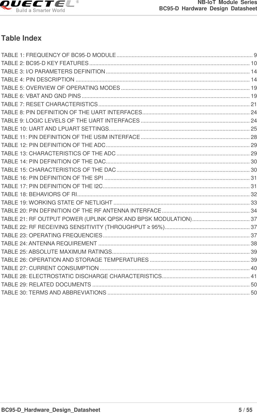
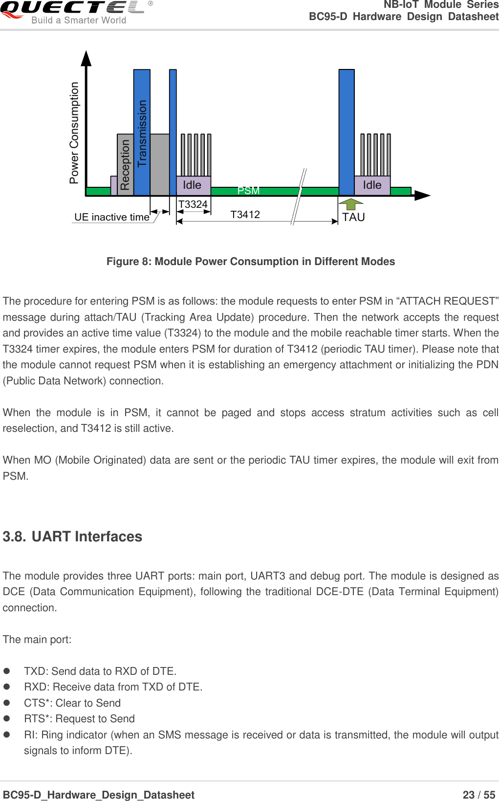
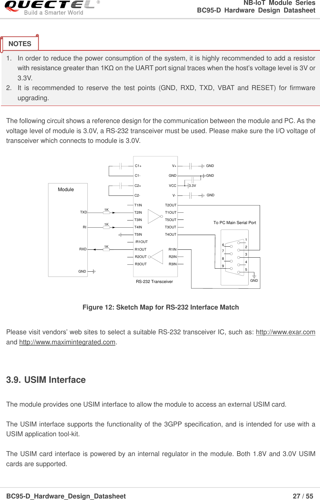
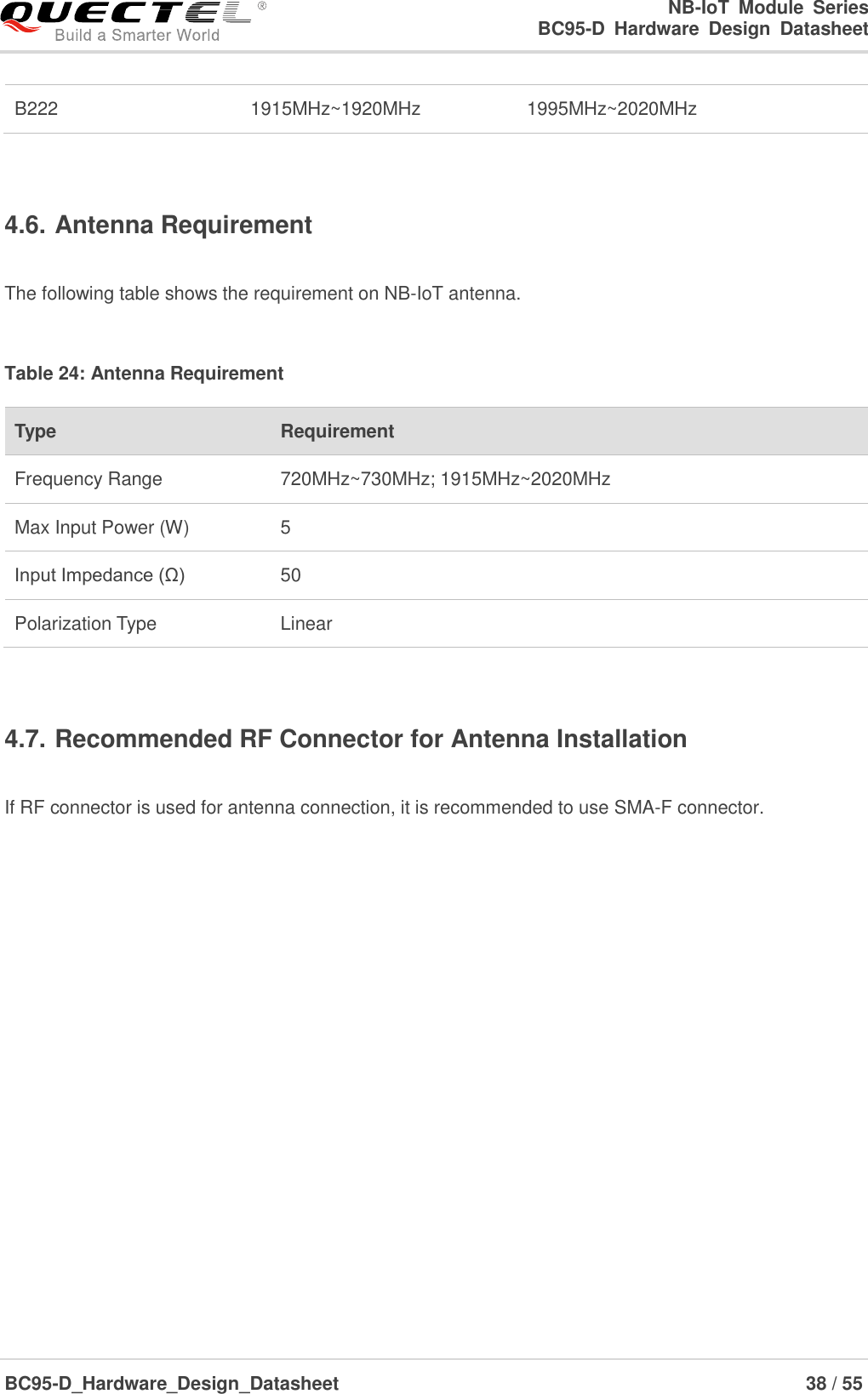
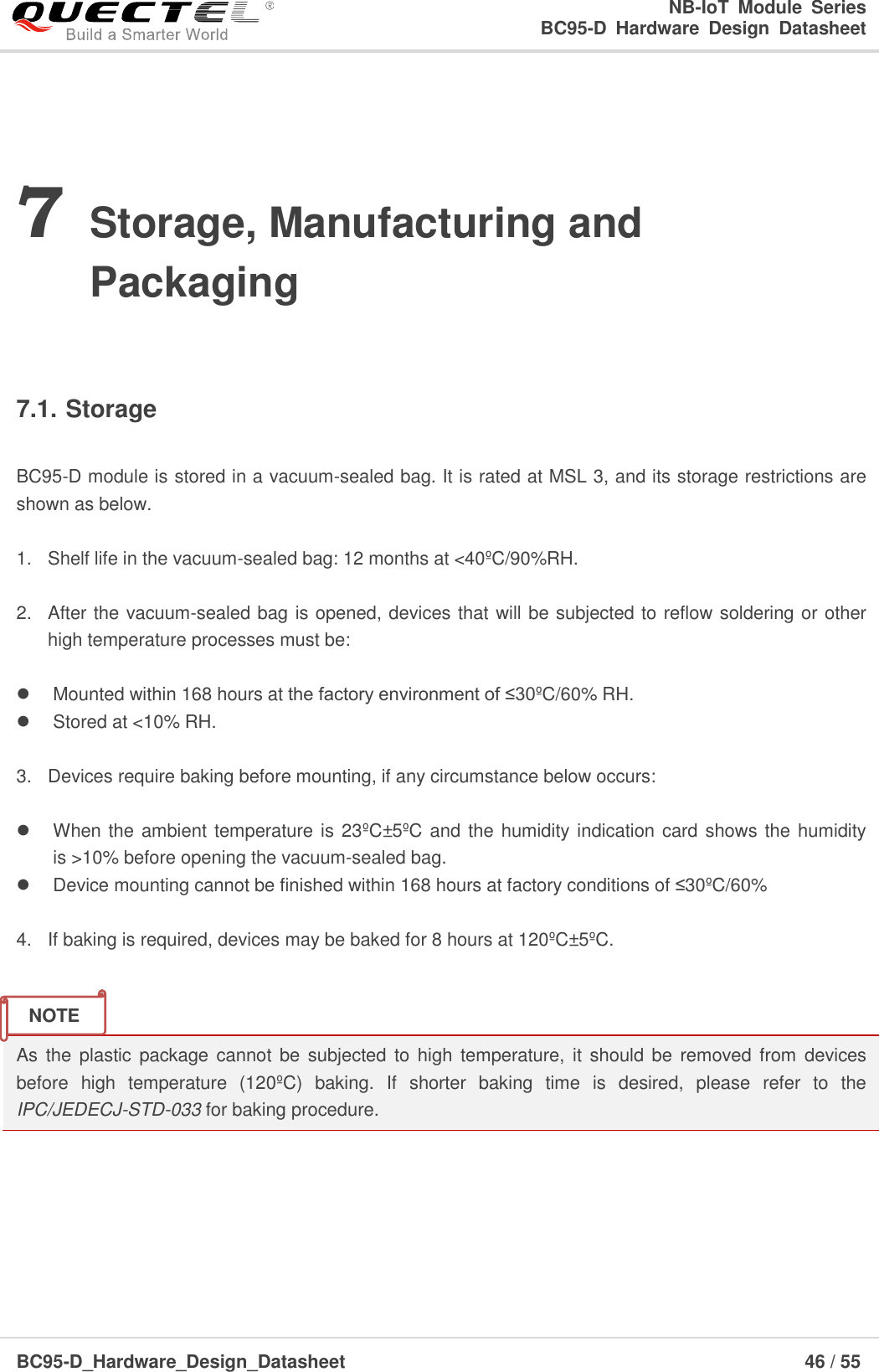
![NB-IoT Module Series BC95-D Hardware Design Datasheet BC95-D_Hardware_Design_Datasheet 26 / 55 3.8.2. Debug Port The debug port is used to view log information with the UEMonitor tool for firmware debugging, and the baud rate is 921600bps. For detailed usage of the UEMonitor, please refer to document [3]. A reference design for debug port is shown as below. DBG_TXDDBG_RXDDBG_TXDDBG_RXDModule (DCE)Serial portDebug portGND GNDPC (DTE) Figure 10: Reference Design for Debug Port 3.8.3. UART Application A reference design of 3.3V level match is shown as below. PeripheralTXDRXD1KTXDRXDRIEINTModuleVoltage level: 3.3V1K1KGND GNDTXDRXD GNDTest points RESETVBAT VBATRESET Figure 11: Level Match Design for 3.3V System](https://usermanual.wiki/Quectel-Wireless-Solutions/201807BC95D/User-Guide-3924973-Page-27.png)
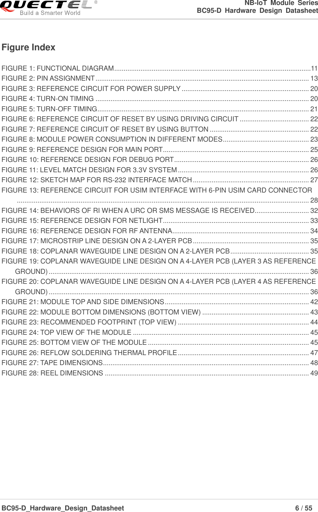
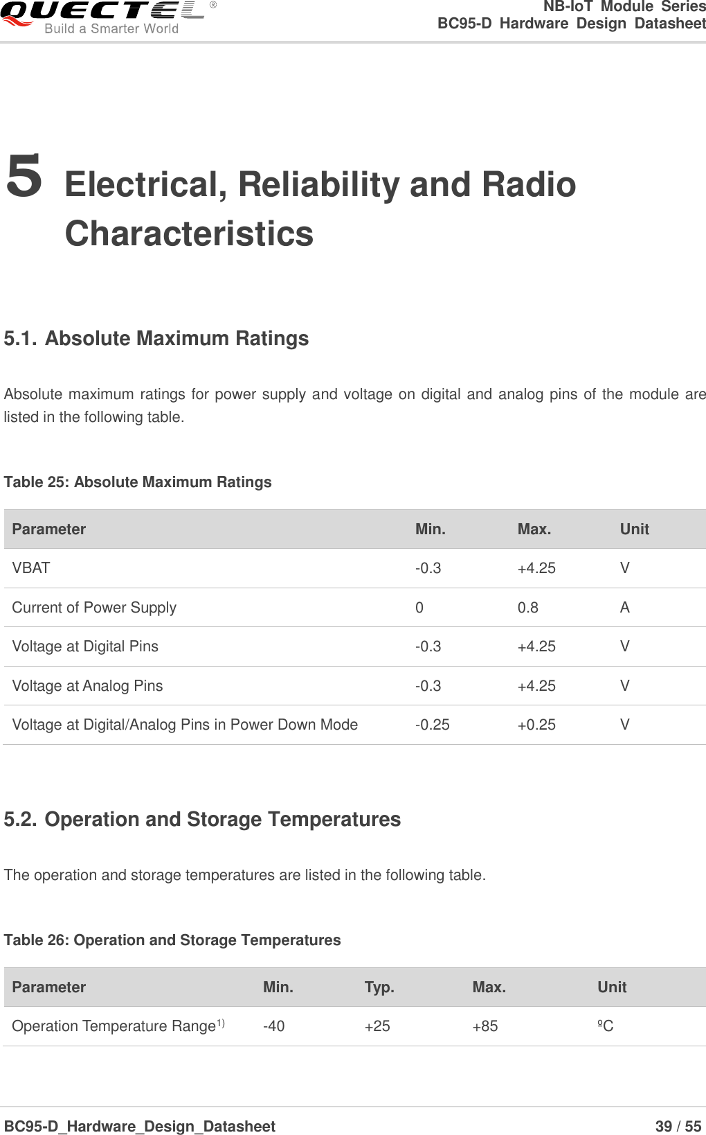
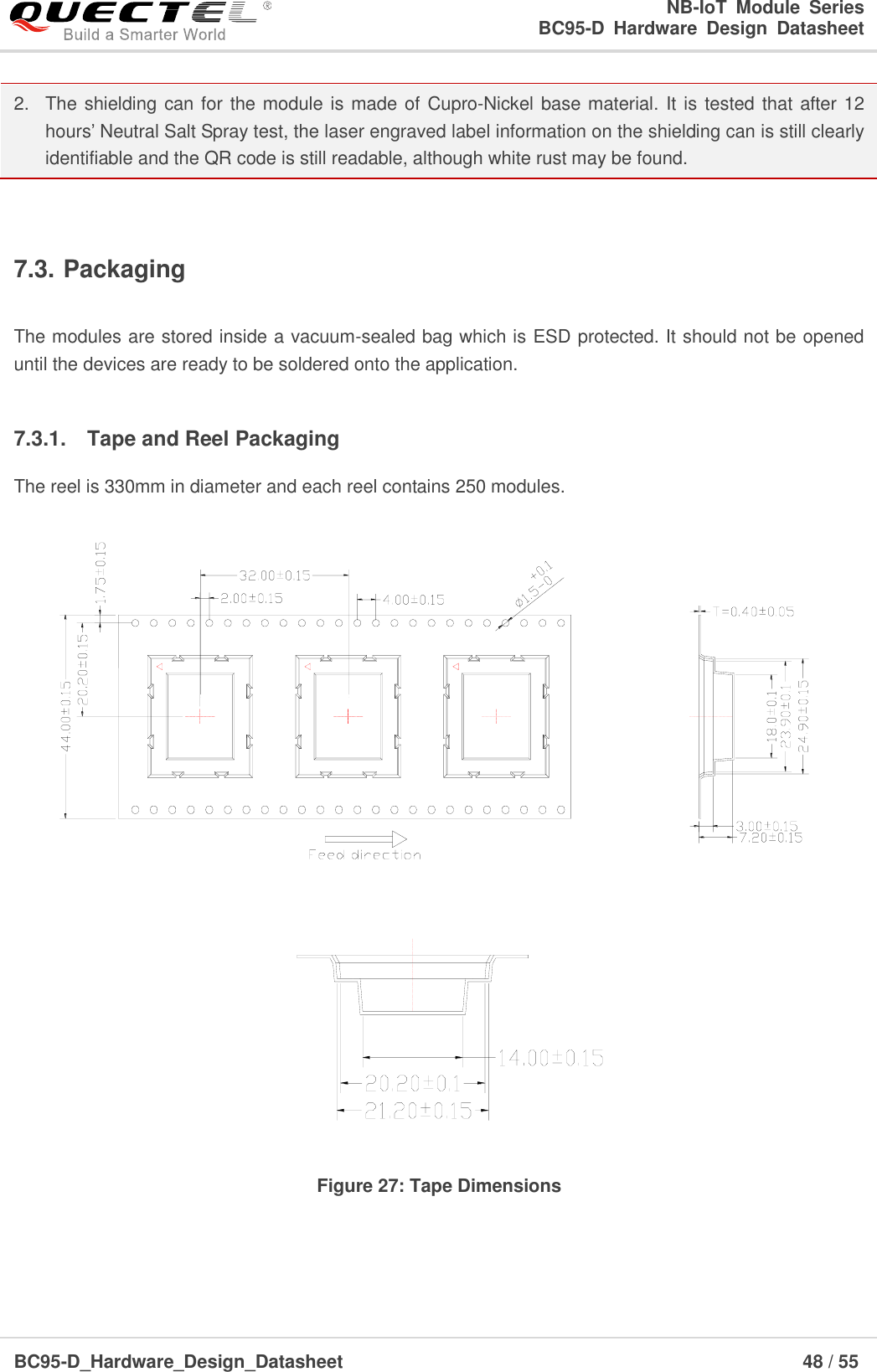
![NB-IoT Module Series BC95-D Hardware Design Datasheet BC95-D_Hardware_Design_Datasheet 36 / 55 Figure 19: Coplanar Waveguide Line Design on a 4-layer PCB (Layer 3 as Reference Ground) Figure 20: Coplanar Waveguide Line Design on a 4-layer PCB (Layer 4 as Reference Ground) In order to ensure RF performance and reliability, the following principles should be complied with in RF layout design: Use an impedance simulation tool to control the characteristic impedance of RF traces as 50Ω±10%. The GND pins adjacent to RF pins should not be designed as thermal relief pads, and should be fully connected to ground. The distance between the RF pins and the RF connector should be as short as possible, and all the right angle traces should be changed to curved ones. There should be clearance area under the signal pin of the antenna connector or solder joint. The reference ground of RF traces should be complete. Meanwhile, adding some ground vias around RF traces and the reference ground could help to improve RF performance. The distance between the ground vias and RF traces should be no less than two times the width of RF signal traces (2*W). For more details about RF layout, please refer to document [5].](https://usermanual.wiki/Quectel-Wireless-Solutions/201807BC95D/User-Guide-3924973-Page-37.png)
![NB-IoT Module Series BC95-D Hardware Design Datasheet BC95-D_Hardware_Design_Datasheet 47 / 55 7.2. Manufacturing and Soldering Push the squeegee to apply the solder paste on the surface of stencil, thus making the paste fill the stencil openings and then penetrate to the PCB. The force on the squeegee should be adjusted properly so as to produce a clean stencil surface on a single pass. To ensure the module soldering quality, the thickness of stencil for the module is recommended to be 0.15mm. For more details, please refer to document [4]. It is suggested that the peak reflow temperature is 235ºC ~245ºC (for SnAg3.0Cu0.5 alloy). The absolute max reflow temperature is 260ºC. To avoid damage to the module caused by repeatedly heating, it is suggested that the module should be mounted after reflow soldering for the other side of PCB has been completed. Recommended reflow soldering thermal profile is shown below. Time50 100 150 200 250 30050100150200250 160ºC 200ºC217070s~120s40s~60sBetween 1~3ºC/sPreheat Heating CoolingºCsLiquids Temperature Temperature Figure 26: Reflow Soldering Thermal Profile 1. During manufacturing and soldering, or any other processes that may contact the module directly, NEVER wipe the module’s shielding can with organic solvents, such as acetone, ethyl alcohol, isopropyl alcohol, trichloroethylene, etc. Otherwise, the shielding can may become rusted. NOTES](https://usermanual.wiki/Quectel-Wireless-Solutions/201807BC95D/User-Guide-3924973-Page-48.png)
![NB-IoT Module Series BC95-D Hardware Design Datasheet BC95-D_Hardware_Design_Datasheet 50 / 55 8 Appendix A References Table 29: Related Documents Table 30: Terms and Abbreviations SN Document Name Remark [1] Quectel_BC95-D_AT_Commands_Manual BC95-D AT Commands Manual [2] Quectel_BC95-D_Firmware_Upgrade_User_Guide BC95-D Firmware Upgrade User Guide [3] Quectel_BC95-D_UEMonitor_User_Guide BC95-D UEMonitor User Guide [4] Quectel_Module_Secondary_SMT_User_Guide Module Secondary SMT User Guide [5] Quectel_RF_Layout_Application_Note RF Layout Application Note [6] NL-002871-SP-2C-Hi2115 C30 Datasheet Datasheet on which this document is based [7] Quectel_BC95-D_Reference_Design BC95-D Reference Design Abbreviation Description ADC Analog-to-Digital Converter AS Access Stratum DAC Digital-to-Analog Converter DCE Data Communications Equipment (typically module) DNL Differential Nonlinearity DTE Data Terminal Equipment (typically computer, external controller) DRX Discontinuous Reception H-FDD Half Frequency Division Duplexing](https://usermanual.wiki/Quectel-Wireless-Solutions/201807BC95D/User-Guide-3924973-Page-51.png)