Quectel Wireless Solutions 201807BC95D NB-IoT Module User Manual
Quectel Wireless Solutions Company Limited NB-IoT Module Users Manual
Users Manual


NB-IoT Module Series
BC95-D Hardware Design Datasheet
BC95-D_Hardware_Design_Datasheet 1 / 55
Our aim is to provide customers with timely and comprehensive service. For any
assistance, please contact our company headquarters:
Quectel Wireless Solutions Co., Ltd.
7th Floor, Hongye Building, No.1801 Hongmei Road, Xuhui District, Shanghai 200233, China
Tel: +86 21 5108 6236
Email: info@quectel.com
Or our local office. For more information, please visit:
http://quectel.com/support/sales.htm
For technical support, or to report documentation errors, please visit:
http://quectel.com/support/technical.htm
Or email to: support@quectel.com
GENERAL NOTES
QUECTEL OFFERS THE INFORMATION AS A SERVICE TO ITS CUSTOMERS. THE INFORMATION
PROVIDED IS BASED UPON CUSTOMERS’ REQUIREMENTS. QUECTEL MAKES EVERY EFFORT
TO ENSURE THE QUALITY OF THE INFORMATION IT MAKES AVAILABLE. QUECTEL DOES NOT
MAKE ANY WARRANTY AS TO THE INFORMATION CONTAINED HEREIN, AND DOES NOT ACCEPT
ANY LIABILITY FOR ANY INJURY, LOSS OR DAMAGE OF ANY KIND INCURRED BY USE OF OR
RELIANCE UPON THE INFORMATION. ALL INFORMATION SUPPLIED HEREIN IS SUBJECT TO
CHANGE WITHOUT PRIOR NOTICE.
COPYRIGHT
THE INFORMATION CONTAINED HERE IS PROPRIETARY TECHNICAL INFORMATION OF
QUECTEL WIRELESS SOLUTIONS CO., LTD. TRANSMITTING, REPRODUCTION, DISSEMINATION
AND EDITING OF THIS DOCUMENT AS WELL AS UTILIZATION OF THE CONTENT ARE
FORBIDDEN WITHOUT PERMISSION. OFFENDERS WILL BE HELD LIABLE FOR PAYMENT OF
DAMAGES. ALL RIGHTS ARE RESERVED IN THE EVENT OF A PATENT GRANT OR
REGISTRATION OF A UTILITY MODEL OR DESIGN.
Copyright © Quectel Wireless Solutions Co., Ltd. 2018. All rights reserved.
NB-IoT Module Series
BC95-D Hardware Design Datasheet
BC95-D_Hardware_Design_Datasheet 2 / 55
About the Document
History
Revision
Date
Author
Description
1.0
2018-05-03
Ewent LU
Initial
1.1
2018-05-25
Ewent LU
1. Added chip name in Chapter 2.3.
2. Added reference chip datasheet in Table 29.
1.2
2018-06-05
Beny ZHU
Updated the note about RF receiving sensitivity test
condition in Chapter 4.4.
1.3
2018-06-08
Ewent LU
Added “Quectel_BC95-D_Reference_Design” document
as a reference datasheet in Table 29.

NB-IoT Module Series
BC95-D Hardware Design Datasheet
BC95-D_Hardware_Design_Datasheet 3 / 55
Contents
About the Document ................................................................................................................................... 2
Contents ....................................................................................................................................................... 3
Table Index ................................................................................................................................................... 5
Figure Index ................................................................................................................................................. 6
1 Introduction .......................................................................................................................................... 7
1.1. Safety Information ................................................................................................................... 8
2 Product Concept .................................................................................................................................. 9
2.1. General Description ................................................................................................................. 9
2.2. Key Features ........................................................................................................................... 9
2.3. Functional Diagram ............................................................................................................... 11
2.4. Evaluation Board ................................................................................................................... 11
3 Application Functions ....................................................................................................................... 12
3.1. General Description ............................................................................................................... 12
3.2. Pin Assignment ...................................................................................................................... 13
3.3. Pin Description ...................................................................................................................... 14
3.4. Operating Modes ................................................................................................................... 18
3.5. Power Supply ........................................................................................................................ 19
3.5.1. Power Supply Pins ......................................................................................................... 19
3.5.2. Reference Design for Power Supply .............................................................................. 19
3.6. Turn on and off Scenarios ..................................................................................................... 20
3.6.1. Turn on ........................................................................................................................... 20
3.6.2. Turn off ........................................................................................................................... 21
3.6.3. Reset the Module ........................................................................................................... 21
3.7. Power Saving Mode (PSM) ................................................................................................... 22
3.8. UART Interfaces .................................................................................................................... 23
3.8.1. Main Port ........................................................................................................................ 25
3.8.2. Debug Port ..................................................................................................................... 26
3.8.3. UART Application ........................................................................................................... 26
3.9. USIM Interface ....................................................................................................................... 27
3.10. ADC Interface ........................................................................................................................ 29
3.11. DAC Interface ........................................................................................................................ 30
3.12. SPI Interface .......................................................................................................................... 31
3.13. I2C Interface .......................................................................................................................... 31
3.14. Behaviors of RI ...................................................................................................................... 32
3.15. Network Status Indication ...................................................................................................... 33
4 Antenna Interface ............................................................................................................................... 34
4.1. RF Antenna Reference Design ............................................................................................. 34
4.2. Reference Design of RF Layout ............................................................................................ 35
4.3. RF Output Power ................................................................................................................... 37

NB-IoT Module Series
BC95-D Hardware Design Datasheet
BC95-D_Hardware_Design_Datasheet 4 / 55
4.4. RF Receiving Sensitivity ........................................................................................................ 37
4.5. Operating Frequencies .......................................................................................................... 37
4.6. Antenna Requirement ........................................................................................................... 38
4.7. Recommended RF Connector for Antenna Installation ........................................................ 38
5 Electrical, Reliability and Radio Characteristics ............................................................................ 39
5.1. Absolute Maximum Ratings................................................................................................... 39
5.2. Operation and Storage Temperatures ................................................................................... 39
5.3. Current Consumption ............................................................................................................ 40
5.4. Electrostatic Discharge .......................................................................................................... 40
6 Mechanical Dimensions .................................................................................................................... 42
6.1. Mechanical Dimensions of the Module ................................................................................. 42
6.2. Recommended Footprint ....................................................................................................... 44
6.3. Design Effect Drawings of the Module .................................................................................. 45
7 Storage, Manufacturing and Packaging .......................................................................................... 46
7.1. Storage .................................................................................................................................. 46
7.2. Manufacturing and Soldering ................................................................................................ 47
7.3. Packaging .............................................................................................................................. 48
7.3.1. Tape and Reel Packaging .............................................................................................. 48
8 Appendix A References ..................................................................................................................... 50

NB-IoT Module Series
BC95-D Hardware Design Datasheet
BC95-D_Hardware_Design_Datasheet 5 / 55
Table Index
TABLE 1: FREQUENCY OF BC95-D MODULE .......................................................................................... 9
TABLE 2: BC95-D KEY FEATURES .......................................................................................................... 10
TABLE 3: I/O PARAMETERS DEFINITION ............................................................................................... 14
TABLE 4: PIN DESCRIPTION ................................................................................................................... 14
TABLE 5: OVERVIEW OF OPERATING MODES ..................................................................................... 19
TABLE 6: VBAT AND GND PINS ............................................................................................................... 19
TABLE 7: RESET CHARACTERISTICS .................................................................................................... 21
TABLE 8: PIN DEFINITION OF THE UART INTERFACES ....................................................................... 24
TABLE 9: LOGIC LEVELS OF THE UART INTERFACES ........................................................................ 24
TABLE 10: UART AND LPUART SETTINGS ............................................................................................. 25
TABLE 11: PIN DEFINITION OF THE USIM INTERFACE ........................................................................ 28
TABLE 12: PIN DEFINITION OF THE ADC ............................................................................................... 29
TABLE 13: CHARACTERISTICS OF THE ADC ........................................................................................ 29
TABLE 14: PIN DEFINITION OF THE DAC ............................................................................................... 30
TABLE 15: CHARACTERISTICS OF THE DAC ........................................................................................ 30
TABLE 16: PIN DEFINITION OF THE SPI ................................................................................................ 31
TABLE 17: PIN DEFINITION OF THE I2C ................................................................................................. 31
TABLE 18: BEHAVIORS OF RI .................................................................................................................. 32
TABLE 19: WORKING STATE OF NETLIGHT .......................................................................................... 33
TABLE 20: PIN DEFINITION OF THE RF ANTENNA INTERFACE .......................................................... 34
TABLE 21: RF OUTPUT POWER (UPLINK QPSK AND BPSK MODULATION) ...................................... 37
TABLE 22: RF RECEIVING SENSITIVITY (THROUGHPUT ≥ 95%) ........................................................ 37
TABLE 23: OPERATING FREQUENCIES ................................................................................................. 37
TABLE 24: ANTENNA REQUIREMENT .................................................................................................... 38
TABLE 25: ABSOLUTE MAXIMUM RATINGS ........................................................................................... 39
TABLE 26: OPERATION AND STORAGE TEMPERATURES .................................................................. 39
TABLE 27: CURRENT CONSUMPTION ................................................................................................... 40
TABLE 28: ELECTROSTATIC DISCHARGE CHARACTERISTICS .......................................................... 41
TABLE 29: RELATED DOCUMENTS ........................................................................................................ 50
TABLE 30: TERMS AND ABBREVIATIONS .............................................................................................. 50

NB-IoT Module Series
BC95-D Hardware Design Datasheet
BC95-D_Hardware_Design_Datasheet 6 / 55
Figure Index
FIGURE 1: FUNCTIONAL DIAGRAM .........................................................................................................11
FIGURE 2: PIN ASSIGNMENT .................................................................................................................. 13
FIGURE 3: REFERENCE CIRCUIT FOR POWER SUPPLY .................................................................... 20
FIGURE 4: TURN-ON TIMING .................................................................................................................. 20
FIGURE 5: TURN-OFF TIMING ................................................................................................................. 21
FIGURE 6: REFERENCE CIRCUIT OF RESET BY USING DRIVING CIRCUIT ..................................... 22
FIGURE 7: REFERENCE CIRCUIT OF RESET BY USING BUTTON ..................................................... 22
FIGURE 8: MODULE POWER CONSUMPTION IN DIFFERENT MODES .............................................. 23
FIGURE 9: REFERENCE DESIGN FOR MAIN PORT .............................................................................. 25
FIGURE 10: REFERENCE DESIGN FOR DEBUG PORT ........................................................................ 26
FIGURE 11: LEVEL MATCH DESIGN FOR 3.3V SYSTEM ...................................................................... 26
FIGURE 12: SKETCH MAP FOR RS-232 INTERFACE MATCH .............................................................. 27
FIGURE 13: REFERENCE CIRCUIT FOR USIM INTERFACE WITH 6-PIN USIM CARD CONNECTOR
............................................................................................................................................................ 28
FIGURE 14: BEHAVIORS OF RI WHEN A URC OR SMS MESSAGE IS RECEIVED............................. 32
FIGURE 15: REFERENCE DESIGN FOR NETLIGHT .............................................................................. 33
FIGURE 16: REFERENCE DESIGN FOR RF ANTENNA ......................................................................... 34
FIGURE 17: MICROSTRIP LINE DESIGN ON A 2-LAYER PCB .............................................................. 35
FIGURE 18: COPLANAR WAVEGUIDE LINE DESIGN ON A 2-LAYER PCB .......................................... 35
FIGURE 19: COPLANAR WAVEGUIDE LINE DESIGN ON A 4-LAYER PCB (LAYER 3 AS REFERENCE
GROUND) ........................................................................................................................................... 36
FIGURE 20: COPLANAR WAVEGUIDE LINE DESIGN ON A 4-LAYER PCB (LAYER 4 AS REFERENCE
GROUND) ........................................................................................................................................... 36
FIGURE 21: MODULE TOP AND SIDE DIMENSIONS ............................................................................. 42
FIGURE 22: MODULE BOTTOM DIMENSIONS (BOTTOM VIEW) ......................................................... 43
FIGURE 23: RECOMMENDED FOOTPRINT (TOP VIEW) ...................................................................... 44
FIGURE 24: TOP VIEW OF THE MODULE .............................................................................................. 45
FIGURE 25: BOTTOM VIEW OF THE MODULE ...................................................................................... 45
FIGURE 26: REFLOW SOLDERING THERMAL PROFILE ...................................................................... 47
FIGURE 27: TAPE DIMENSIONS .............................................................................................................. 48
FIGURE 28: REEL DIMENSIONS ............................................................................................................. 49

NB-IoT Module Series
BC95-D Hardware Design Datasheet
BC95-D_Hardware_Design_Datasheet 7 / 55
1 Introduction
This document defines the BC95-D module and describes its air interface and hardware interface which
are connected with customers’ applications.
This document can help customers to quickly understand module interface specifications, electrical and
mechanical details, as well as other related information of the module. Associated with application note
and user guide, customers can use the BC95-D module to design and set up mobile applications easily.

NB-IoT Module Series
BC95-D Hardware Design Datasheet
BC95-D_Hardware_Design_Datasheet 8 / 55
1.1. Safety Information
The following safety precautions must be observed during all phases of the operation, such as usage,
service or repair of any cellular terminal or mobile incorporating BC95-D module. Manufacturers of the
cellular terminal should send the following safety information to users and operating personnel, and
incorporate these guidelines into all manuals supplied with the product. If not so, Quectel assumes no
liability for the customers’ failure to comply with these precautions.
Full attention must be given to driving at all times in order to reduce the risk of an
accident. Using a mobile while driving (even with a handsfree kit) causes
distraction and can lead to an accident. You must comply with laws and regulations
restricting the use of wireless devices while driving.
Switch off the cellular terminal or mobile before boarding an aircraft. Make sure it is
switched off. The operation of wireless appliances in an aircraft is forbidden, so as
to prevent interference with communication systems. Consult the airline staff about
the use of wireless devices on boarding the aircraft, if your device offers an
Airplane Mode which must be enabled prior to boarding an aircraft.
Switch off your wireless device when in hospitals, clinics or other health care
facilities. These requests are designed to prevent possible interference with
sensitive medical equipment.
Cellular terminals or mobiles operating over radio frequency signal and cellular
network cannot be guaranteed to connect in all conditions, for example no mobile
fee or with an invalid (U)SIM card. While you are in this condition and need
emergent help, please remember using emergency call. In order to make or
receive a call, the cellular terminal or mobile must be switched on and in a service
area with adequate cellular signal strength.
Your cellular terminal or mobile contains a transmitter and receiver. When it is ON,
it receives and transmits radio frequency energy. RF interference can occur if it is
used close to TV set, radio, computer or other electric equipment.
In locations with potentially explosive atmospheres, obey all posted signs to turn
off wireless devices such as your phone or other cellular terminals. Areas with
potentially explosive atmospheres include fuelling areas, below decks on boats,
fuel or chemical transfer or storage facilities, areas where the air contains
chemicals or particles such as grain, dust or metal powders, etc.

NB-IoT Module Series
BC95-D Hardware Design Datasheet
BC95-D_Hardware_Design_Datasheet 9 / 55
2 Product Concept
2.1. General Description
BC95-D is a high-performance NB-IoT module with low power consumption. It supports two frequency
bands as illustrated in the table below. The module is designed to communicate with mobile network
operators’ infrastructure equipment through the NB-IoT radio protocol (3GPP Rel.14).
Table 1: Frequency of BC95-D Module
BC95-D is an SMD type module with LCC package, and comes with an ultra-compact profile of 23.6mm ×
19.9mm × 2.2mm, making it can be easily embedded into applications. It provides hardware interfaces
such as UART interfaces, and can meet almost all the requirements for IoT applications, such as smart
metering, bike sharing, smart parking, smart city, security and asset tracking, home appliances,
agricultural and environmental monitoring, etc.
Designed with power saving technique, the BC95-D consumes an ultra-low current of 5uA in PSM (Power
Saving Mode).
The module fully complies with the RoHS directive of the European Union.
2.2. Key Features
The following table describes the detailed features of BC95-D module.
Frequency Bands
Transmit
Receive
B111
1915MHz~1920MHz
722MHz~728MHz
B222
1915MHz~1920MHz
1995MHz~2020MHz
NB-IoT Module Series
BC95-D Hardware Design Datasheet
BC95-D_Hardware_Design_Datasheet 10 / 55
Table 2: BC95-D Key Features
1) Within operation temperature range, the module is 3GPP compliant.
Feature
Details
Power Supply
Supply voltage: 3.1V~4.2V
Typical supply voltage: 3.6V
Power Saving Mode
Maximum power consumption in PSM: 15uW
Transmitting Power
23dBm±2dB
Temperature Range
Operation temperature range: -40°C ~ +85°C 1)
Storage temperature range: -40°C ~ +90°C
USIM Interface
Supports Class B USIM card: 1.8V/3.0V
UART Interfaces
Main port:
When used for AT command communication and data transmission,
the baud rate supports 4800bps, 9600bps and 115200bps, and the
default baud rate is 9600bps
When used for firmware upgrading, the baud rate is 921600bps
Debug port:
Used for firmware debugging
Only supports 921600bps baud rate
UART3:
Used for communication with peripheral
Internet Protocol Features
Supports IPv4/IPv6/UDP/Non-IP/TCP
SMS
Text and PDU mode
Point to point MO and MT
Data Transmission Feature
Single tone with 15kHz/3.75kHz subcarrier: 25.2kbps (DL)/
15.625kbps (UL)
Multi tone with 15kHz subcarrier: 25.2kbps (DL)/54kbps (UL)
AT Commands
Compliant with 3GPP TS 27.007 V14.3.0 (2017-03) and Quectel AT
commands
Physical Characteristics
Size: (23.6±0.15) mm × (19.9±0.15) mm × (2.2±0.2) mm
Weight: 1.8g±0.2g
Firmware Upgrade
Firmware upgrade via UART
Antenna Interface
50Ω impedance control
RoHS
All hardware components are fully compliant with EU RoHS directive
NOTE
NB-IoT Module Series
BC95-D Hardware Design Datasheet
BC95-D_Hardware_Design_Datasheet 11 / 55
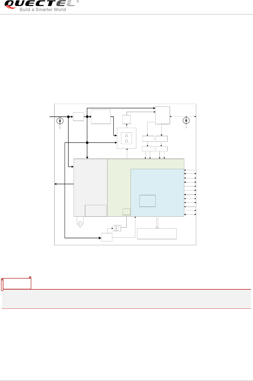
2.3. Functional Diagram
The following figure shows a block diagram of BC95-D and illustrates the major functional parts.
Radio frequency
Baseband
Power management
Peripheral interfaces
RF_ANT
Switch
RX_Filter
RF_PA
VBAT
PMU
DCDC
32K
LDO
RF TRansceiver and Analogue
VDD_EXT
TCXO
38.4M
XTAL
Driver
Baseband
RESET
UARTx2
Debug UART
USIM
Flash
SRAM
SPI
SPI Flash
NETLIGHT
ADC
SPI
RI
DAC
TX
Filter
RX_Filter
(Optional)
Load
Switch APT DCDC
I2C
GPIO
SWD
Balance Balance
Figure 1: Functional Diagram
PA model: SKY77761.
Baseband chip: Hi2115GBCV110.
2.4. Evaluation Board
In order to help customers develop applications with BC95-D, Quectel supplies the evaluation board
(EVB), USB cable, antenna and other peripherals to control or test the module.
NOTE

NB-IoT Module Series
BC95-D Hardware Design Datasheet
BC95-D_Hardware_Design_Datasheet 12 / 55
3 Application Functions
3.1. General Description
BC95-D is equipped with 54 LCC pads (with 1.1mm pitch) and 40 LGA pads (with 1.7mm pitch). The
following chapters provide detailed descriptions of these pins:
Power supply
UART interfaces
USIM interface
ADC interface
DAC interface
SPI interface
I2C interface
Network status indication
RF interface
NB-IoT Module Series
BC95-D Hardware Design Datasheet
BC95-D_Hardware_Design_Datasheet 13 / 55
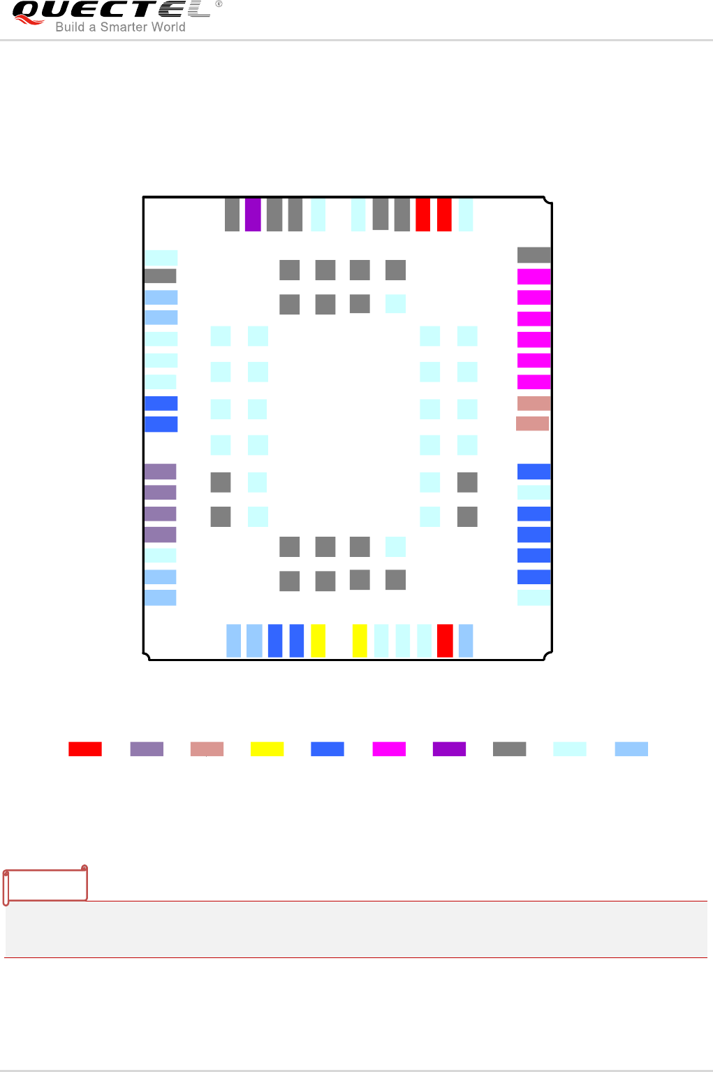
3.2. Pin Assignment
44
45
46
47
48
51
52
53
54
50
49
43
42
41
40
39
38
35
36
37
34
33
32
31
30
29
28
27
26
25
24
23
22
21
20
19
18
17
9
8
SWD_CLK
SWD_IO
SPI_MOSI
SPI_CLK
RESERVED
RESET
RIO*
2
10
11
12
13
14
15
16
UART3_RXD
PIO1
NETLIGHT
DBG_RXD
DBG_TXD
ADC
DAC
RESERVED
RESERVED
RESERVED
VDD_EXT
PIO2
USIM_CLK
USIM_DATA
USIM_RST
USIM_VDD
RI
RESERVED
CTS*
TXD
RXD
RESERVED
USIM_GND
GND
UART3_TXD
GND
SPI_CS
SPI_MISO
RTS*
I2C_SCL
I2C_SDA
GND
RF_ANT
GND
GND
RESERVED
VBAT
VBAT
GND
GND
RESERVED
RESERVED
USIM_DETECT
55
56
57
58
59
60
75
76
77
78
79
80
90
89
88
87
86
85
70
69
68
67
66
65
83 84
81 82
63 64
61 62
72 71
74 73
92 91
94 93
POWER ADC/DAC UART USIM OTHERSGND RESERVED
ANTI2CSPI
1
RESERVED
5
6
7
RESERVED
RESERVED
RESERVED
3
4
7
Figure 2: Pin Assignment
1. Keep all reserved pins unconnected.
2. “*” means under development.
NOTES

NB-IoT Module Series
BC95-D Hardware Design Datasheet
BC95-D_Hardware_Design_Datasheet 14 / 55
3.3. Pin Description
The following tables show the pin definition and description of BC95-D.
Table 3: I/O Parameters Definition
Table 4: Pin Description
Type
Description
IO
Bidirectional
DI
Digital input
DO
Digital output
PI
Power input
PO
Power output
AI
Analog input
AO
Analog output
OD
Open drain
Power Supply
Pin Name
Pin No.
I/O
Description
DC Characteristics
Comment
VBAT
45, 46
PI
Main power
supply of the
module:
VBAT=3.1V~
4.2V
Vmax=4.2V
Vmin=3.1V
Vnorm=3.6V
The power supply
must be able to
provide sufficient
current up to 0.8A.
VDD_
EXT
26
PO
Supply 3.0V
voltage for
external circuits
Vmax=3.3V
Vmin=2.7V
Vnorm=3V
IOmax=20mA
If it is used for
power supply, a
2.2uF~4.7uF
bypass capacitor
is recommended
to be added in
active and idle
modes. In PSM, it
cannot be used for

NB-IoT Module Series
BC95-D Hardware Design Datasheet
BC95-D_Hardware_Design_Datasheet 15 / 55
power supply.
If unused, keep
this pin open.
GND
2, 43, 47, 48,
51, 52, 54,
59~66,
71~74,
81~83, 92~94
Ground
Reset Interface
Pin Name
Pin No.
I/O
Description
DC Characteristics
Comment
RESET
15
DI
Reset the
module
RPU≈78kΩ
VIHmax=3.3V
VIHmin=2.1V
VILmax=0.6V
Pull up internally.
Active low.
Network Status Indicator
Pin Name
Pin No.
I/O
Description
DC Characteristics
Comment
NETLIGHT
18
DO
Network status
indication
VOLmax=0.3V
VOHmin=2.4V
If unused, keep
this pin open.
Analog Interface
Pin Name
Pin No.
I/O
Description
DC Characteristics
Comment
ADC
21
AI
General
purpose analog
to digital
converter
interface
Input voltage range:
0V~4.0V
The maximum
input voltage
should be lower
than the VBAT
voltage.
If unused, keep
this pin open.
Minimum input
impedance:
100MΩ
DAC
22
AO
General
purpose digital
to analog
converter
interface
Output voltage range:
Type: 3.5mV
If unused, keep
this pin open.
Main UART Port
Pin Name
Pin No.
I/O
Description
DC Characteristics
Comment

NB-IoT Module Series
BC95-D Hardware Design Datasheet
BC95-D_Hardware_Design_Datasheet 16 / 55
RXD
29
DI
Receive data
VILmax=0.6V
VIHmin=2.1V
VIHmax=3.3V
3.0V power
domain.
TXD
30
DO
Transmit data
VOLmax=0.3V
VOHmin=2.4V
CTS*
31
DI
Clear to Send
VOLmax=0.3V
VOHmin=2.4V
RTS*
32
DO
Request to
Send
VOLmax=0.3V
VOHmin=2.4V
RI
34
DO
Ring indicator
VOLmax=0.3V
VOHmin=2.4V
UART3 Port
Pin Name
Pin No.
I/O
Description
DC Characteristics
Comment
UART3_
TXD
8
DI
Receive data
VOLmax=0.3V
VOHmin=2.4V
VOLmax=0.3V
VOHmin=2.4V
UART3_
RXD
9
DO
Transmit data
VOLmax=0.3V
VOHmin=2.4V
Debug Port
Pin Name
Pin No.
I/O
Description
DC Characteristics
Comment
DBG_
RXD
19
DI
Receive data
VILmax=0.6V
VIHmin=2.1V
VIHmax=3.3V
If unused, keep
these pins open.
DBG_
TXD
20
DO
Transmit data
VOLmax=0.3V
VOHmin=2.4V
If unused, keep
these pins open.
USIM Interface
Pin Name
Pin No.
I/O
Description
DC Characteristics
Comment
USIM_
VDD
38
DO
Power supply
for USIM card
Vnorm=1.8/3.0V
All signals of
USIM interface
should be
protected against
ESD with a TVS
diode array.
Maximum trace
length from the
module pad to
USIM card
connector is
200mm.
USIM_
RST
39
DO
USIM card
reset signal
VOLmax=0.1V×USIM_
VDD
VOHmin=0.8V×USIM_
VDD
USIM_
DATA
40
IO
USIM card data
signal
VOLmax=0.1V×USIM_
VDD
VOHmin=0.8V×USIM_
VDD
VILmin=-0.1V×USIM_
VDD
VILmax=0.2V×USIM_

NB-IoT Module Series
BC95-D Hardware Design Datasheet
BC95-D_Hardware_Design_Datasheet 17 / 55
VDD
VIHmin=0.7V×USIM_
VDD
VIHmax=1.1V×USIM_
VDD
All signals of
USIM interface
should be
protected against
ESD with a TVS
diode array.
Maximum trace
length from the
module pad to
USIM card
connector is
200mm.
USIM_
CLK
41
DO
USIM card
clock signal
VOLmax=0.1V×USIM_
VDD
VOHmin=0.8V×USIM_
VDD
USIM_
DETECT
37
DI
USIM card plug
detect
VILmin=-0.1V×USIM_
VDD
VILmax=0.2V×USIM_
VDD
VIHmin=0.7V×USIM_
VDD
VIHmax=1.1V×USIM_
VDD
USIM_GND
42
Specified
ground for
USIM card
SPI Interface
Pin Name
Pin No.
I/O
Description
DC Characteristics
Comment
SPI_CS
10
DO
SPI chip select
VOLmax=0.3V
VOHmin=2.4V
3.0V power domain.
If unused, keep it
open.
SPI_MISO
11
DI
SPI master
input
VILmin=-0.3V
VILmax=0.6V
VIHmin=2.1V
VIHmax=3.3V
SPI_CLK
12
DO
SPI clock
VOLmax=0.3V
VOHmin=2.4V
SPI_MOSI
13
DO
SPI master
output
VOLmax=0.3V
VOHmin=2.4V
I2C Interface
Pin Name
Pin No.
I/O
Description
DC Characteristics
Comment
I2C_SCL
35
DO
I2C clock
An external pull-up
resistor is required.
3.0V power
domain. If unused,
keep it open.
I2C_SDA
36
IO
I2C data
Other Interfaces
NB-IoT Module Series
BC95-D Hardware Design Datasheet
BC95-D_Hardware_Design_Datasheet 18 / 55
“*” means under development.
3.4. Operating Modes
BC95-D module has three operating modes, which can determine the availability of functions for different
levels of power-saving.
Pin Name
Pin No.
I/O
Description
DC Characteristics
Comment
RIO*
16
IO
Analogue PA
control
input/output
interface
VILmin=-0.3V
VILmax=0.6V
VIHmin=2.1V
VIHmax=3.3V
3.0V power
domain.
If unused, keep it
open.
PIO1
17
IO
General
purpose
input/output
interface
VILmin=-0.3V
VILmax=0.6V
VIHmin=2.1V
VIHmax=3.3V
3.0V power
domain.
If unused, keep it
open.
PIO2
27
IO
General
purpose input
output interface
VILmin=-0.3V
VILmax=0.6V
VIHmin=2.1V
VIHmax=3.3V
3.0V power
domain.
If unused, keep it
open.
RF Interface
Pin Name
Pin No.
I/O
Description
DC Characteristics
Comment
RF_ANT
53
IO
RF antenna
pad
Impedance of 50Ω
RESERVED Pins
Pin Name
Pin No.
I/O
Description
DC Characteristics
Comment
RESERVED
1, 5, 6, 7, 14,
23~25, 28, 33,
44, 49, 50,
55~58,
67~70,
75~80, 84~91
Reserved
Keep these pins
unconnected.
NOTE

NB-IoT Module Series
BC95-D Hardware Design Datasheet
BC95-D_Hardware_Design_Datasheet 19 / 55
Table 5: Overview of Operating Modes
3.5. Power Supply
3.5.1. Power Supply Pins
BC95-D provides two VBAT pins for connection with an external power supply.
The following table shows the VBAT pins and ground pins.
Table 6: VBAT and GND Pins
3.5.2. Reference Design for Power Supply
The power design for the module is very important, as the performance of the module largely depends on
the power source. A low quiescent current LDO which can provide sufficient input current up to 0.5A can
be used as the power supply. Meanwhile, Li-SOCI2 batteries can also be used to supply power for the
module. The power supply range of the module is from 3.1V to 4.2V. Please make sure that the input
voltage will never drop below 3.1V or rise above 4.2V even in burst transmission. If the power voltage
drops below 3.1V or rise above 4.2V, the module will be abnormal.
Mode
Function
Normal Operation
Active
In active mode, all functions of the module are available and all
processors are active. Radio transmission and reception can be
performed. Transitions to idle mode or PSM can be initiated in active
mode.
Idle
In idle mode, the module is in light sleep and network connection is
maintained; paging messages can be received; transitions to active
mode or PSM can be initiated in idle mode.
PSM
In PSM, only the 32kHz RTC is working. The network is disconnected,
and paging messages cannot be received either. When MO (Mobile
Originated) data are sent or the periodic TAU (Tracking Area Update)
timer T3412 expires, the module will be woken up.
Pin Name
Pin No.
Description
Min.
Typ.
Max.
Unit
VBAT
45, 46
Power supply for the module
3.1
3.6
4.2
V
GND
2, 43, 47, 48, 51, 52,
54, 59~66, 71~74,
81~83, 92~94
Ground
-
0
-
V
NB-IoT Module Series
BC95-D Hardware Design Datasheet
BC95-D_Hardware_Design_Datasheet 20 / 55
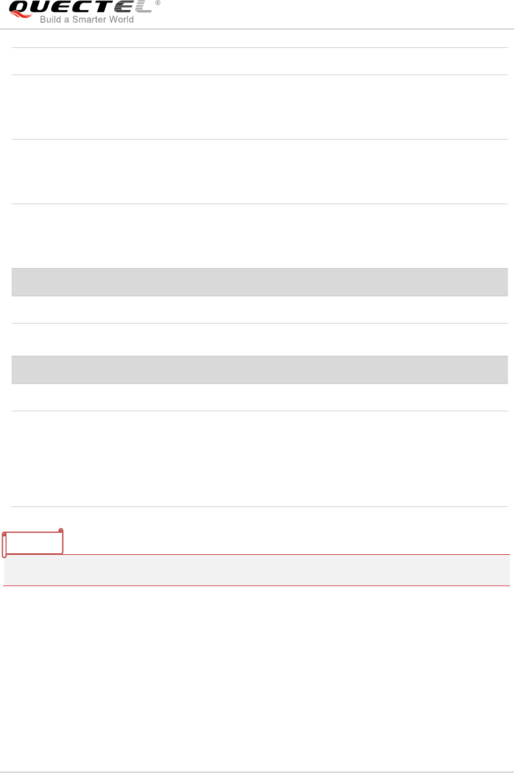
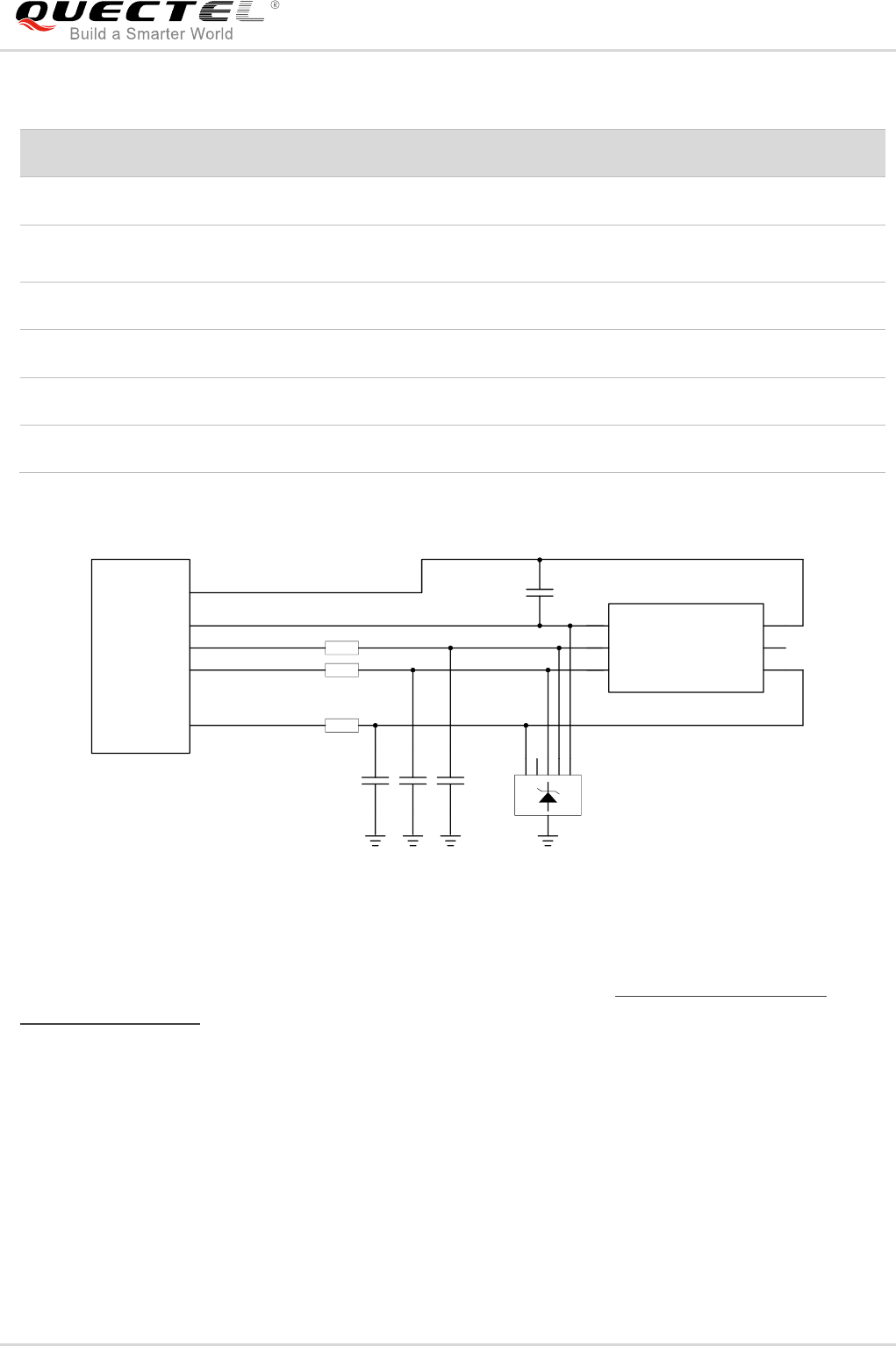
For better power performance, it is recommended to place a 100uF tantalum capacitor with low ESR
(ESR=0.7Ω) and three ceramic capacitors (100nF, 100pF and 22pF) near the VBAT pin, and a TVS diode
also needs to be added on the VBAT trace to increase surge voltage withstand capability. A reference
circuit is illustrated in the following figure. In principle, the longer the VBAT trace is, the wider it will be.
VBAT
C2C1
+C3 C4
GND
100uF 100nF 100pF 22pF
0402 0402
VBAT
Module
GND
D1
WS4.5DPV
Figure 3: Reference Circuit for Power Supply
3.6. Turn on and off Scenarios
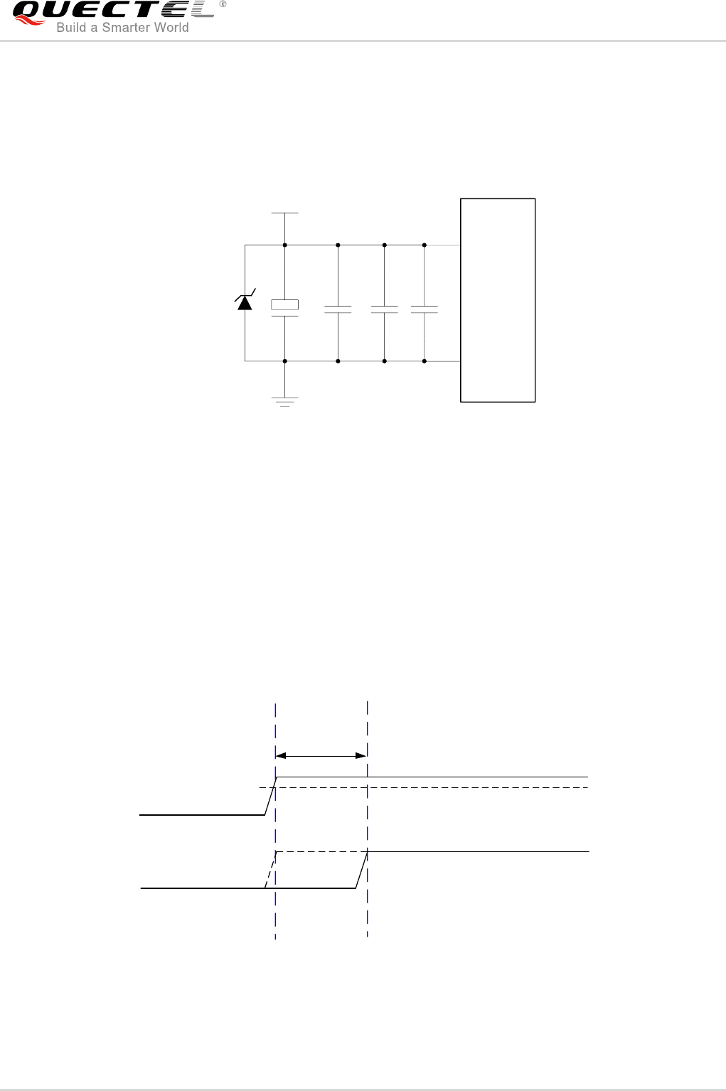
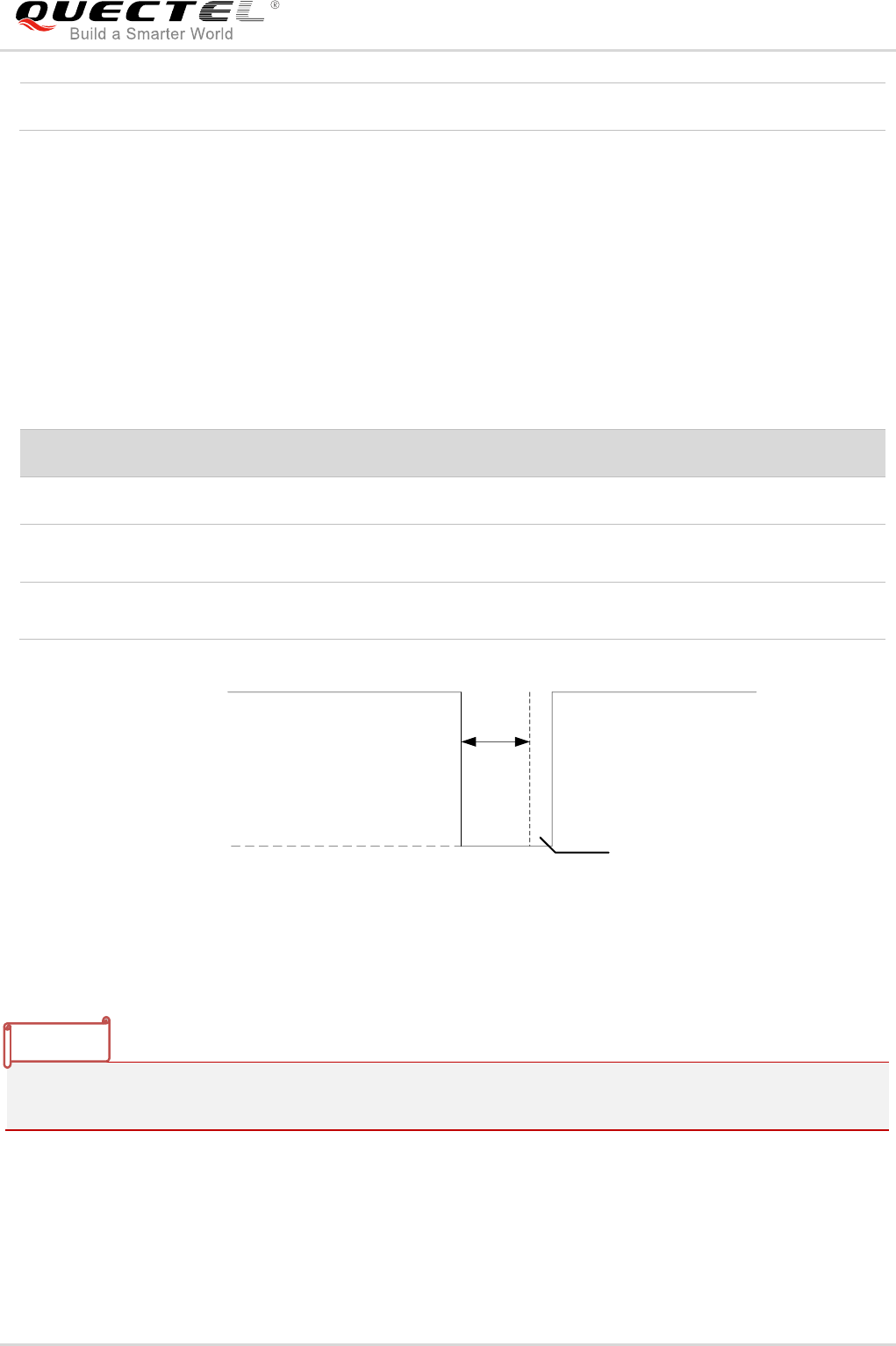
3.6.1. Turn on
The module can be automatically turned on by supplying power source to VBAT pins.
VBAT
RESET
Delay<535us
3.0V
Figure 4: Turn-on Timing
NB-IoT Module Series
BC95-D Hardware Design Datasheet
BC95-D_Hardware_Design_Datasheet 21 / 55
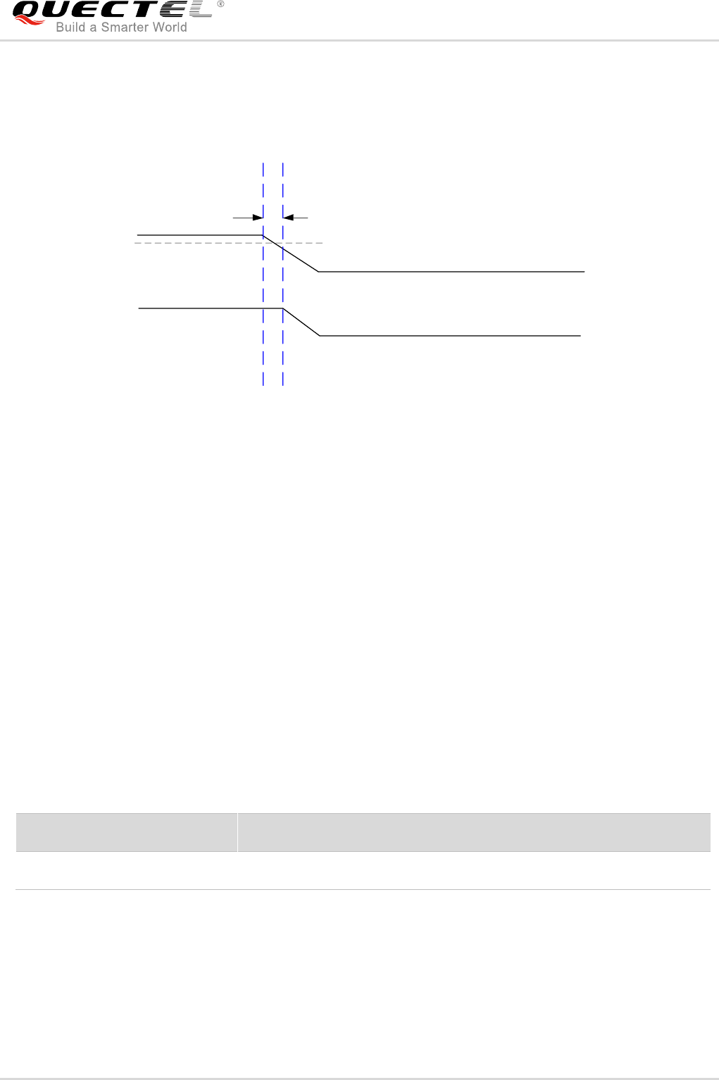
3.6.2. Turn off
The module can be turned off by shutting down the VBAT power supply.
VBAT
RESET
Delay>5ms
3.0V
Figure 5: Turn-off Timing
3.6.3. Reset the Module
The module can be reset by the following two ways. The reset timing is illustrated as the following table.
Hardware
Reset the module by driving the reset pin to a low level voltage for more than 100ms.
Software
Reset the module using command AT+NRB. For more details about the command, please refer to
document [1].
Table 7: Reset Characteristics
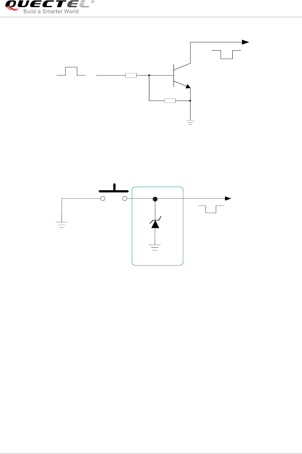
The recommended circuits of hardware resetting are shown as below. An open drain/collector driver or
button can be used to control the RESET pin.
Pin Name
Pin No.
Description
Reset Pull-down Time
RESET
15
Reset the module. Active low
>100ms
NB-IoT Module Series
BC95-D Hardware Design Datasheet
BC95-D_Hardware_Design_Datasheet 22 / 55
Reset pulse
RESET
4.7K
47K
Figure 6: Reference Circuit of RESET by Using Driving Circuit
RESET
S1
Close to S1
TVS
Figure 7: Reference Circuit of RESET by Using Button
3.7. Power Saving Mode (PSM)
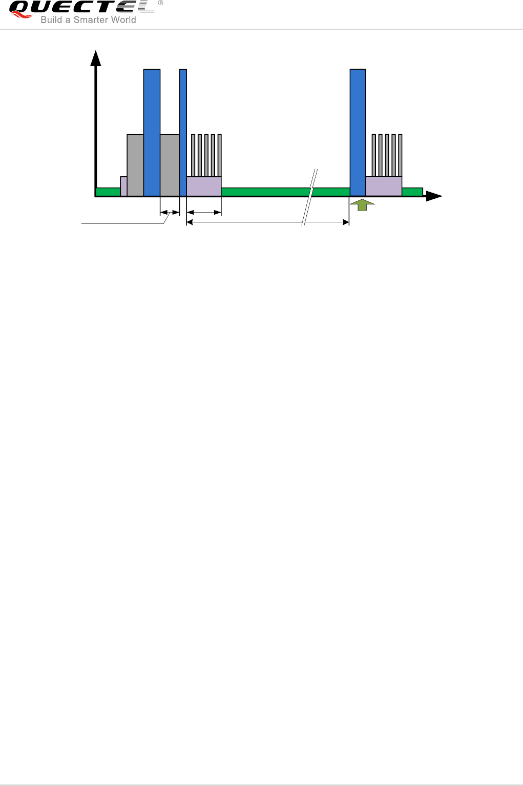
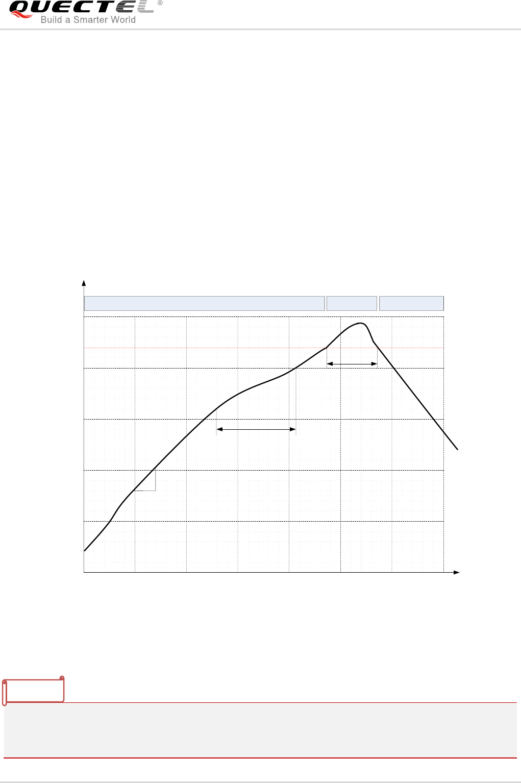
Based on system performance, the module consumes a maximum current of 5uA in PSM. PSM is
designed to reduce power consumption of the module and improve battery life. The following figure shows
the power consumption of the module in different modes.
NB-IoT Module Series
BC95-D Hardware Design Datasheet
BC95-D_Hardware_Design_Datasheet 23 / 55
Power Consumption
PSM
Idle
Transmission
Reception
T3324
T3412 TAU
UE inactive time
Idle
Figure 8: Module Power Consumption in Different Modes
The procedure for entering PSM is as follows: the module requests to enter PSM in “ATTACH REQUEST”
message during attach/TAU (Tracking Area Update) procedure. Then the network accepts the request
and provides an active time value (T3324) to the module and the mobile reachable timer starts. When the
T3324 timer expires, the module enters PSM for duration of T3412 (periodic TAU timer). Please note that
the module cannot request PSM when it is establishing an emergency attachment or initializing the PDN
(Public Data Network) connection.
When the module is in PSM, it cannot be paged and stops access stratum activities such as cell
reselection, and T3412 is still active.
When MO (Mobile Originated) data are sent or the periodic TAU timer expires, the module will exit from
PSM.
3.8. UART Interfaces
The module provides three UART ports: main port, UART3 and debug port. The module is designed as
DCE (Data Communication Equipment), following the traditional DCE-DTE (Data Terminal Equipment)
connection.
The main port:
TXD: Send data to RXD of DTE.
RXD: Receive data from TXD of DTE.
CTS*: Clear to Send
RTS*: Request to Send
RI: Ring indicator (when an SMS message is received or data is transmitted, the module will output
signals to inform DTE).

NB-IoT Module Series
BC95-D Hardware Design Datasheet
BC95-D_Hardware_Design_Datasheet 24 / 55
The UART3 port:
UART3_TXD: Send data to RXD of DTE.
UART3_RXD: Receive data from TXD of DTE.
The debug port:
DBG_TXD: Send data to the COM port of DTE.
DBG_RXD: Receive data from the COM port of DTE.
The logic levels are described in the following table.
Table 8: Pin Definition of the UART Interfaces
Table 9: Logic Levels of the UART Interfaces
Interfaces
Pin No.
Pin Name
Description
Comment
Main Port
29
RXD
Receive data
Power domain: 3.0V
30
TXD
Transmit data
31
CTS*
Clear to Send
32
RTS*
Request to Send
34
RI
Ring indicator
UART3 Port
8
UART3_TXD
Transmit data
9
UART3_RXD
Receive data
Debug Port
19
DBG_RXD
Receive data
20
DBG_TXD
Transmit data
Parameter
Min.
Max.
Unit
VIL
-0.3
0.6
V
VIH
2.1
3.3
V
VOL
0.3
V
VOH
2.4
3.0
V
NB-IoT Module Series
BC95-D Hardware Design Datasheet
BC95-D_Hardware_Design_Datasheet 25 / 55
Table 10: UART and LPUART Settings
1. “*” means under development.
2. 1) 1Mbps baud rate should always be supported, and a higher baud rate can be configured according
to actual needs.
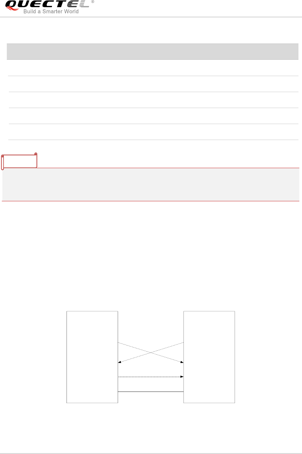
3.8.1. Main Port
The main port can be used for AT command communication and data transmission, and in such case the
baud rate supports 4800bps, 9600bps and 115200bps, and the default baud rate is 9600bps. It can also
be used for firmware upgrading and in such case the baud rate is 921600bps. This main port is available
in active mode, idle mode and PSM. For more information about firmware upgrading, please refer to
document [2].
The following figure shows the connection between the DCE and DTE.
TXD
RXD
RI
TXD
RXD
RING
Module (DCE)
Serial portMain port
GND GND
PC (DTE)
Figure 9: Reference Design for Main Port
Parameter
Supported Value
UART Baud Rate
45.8bps to 3Mbps1)
LPUART Baud Rate
128bps to 57600bps
Parity
Even/Odd/None
Number of Stop Bits
1 or 2 bits
Data Bits Per Frame
5, 6, 7 or 8 bits
NOTES
NB-IoT Module Series
BC95-D Hardware Design Datasheet
BC95-D_Hardware_Design_Datasheet 26 / 55
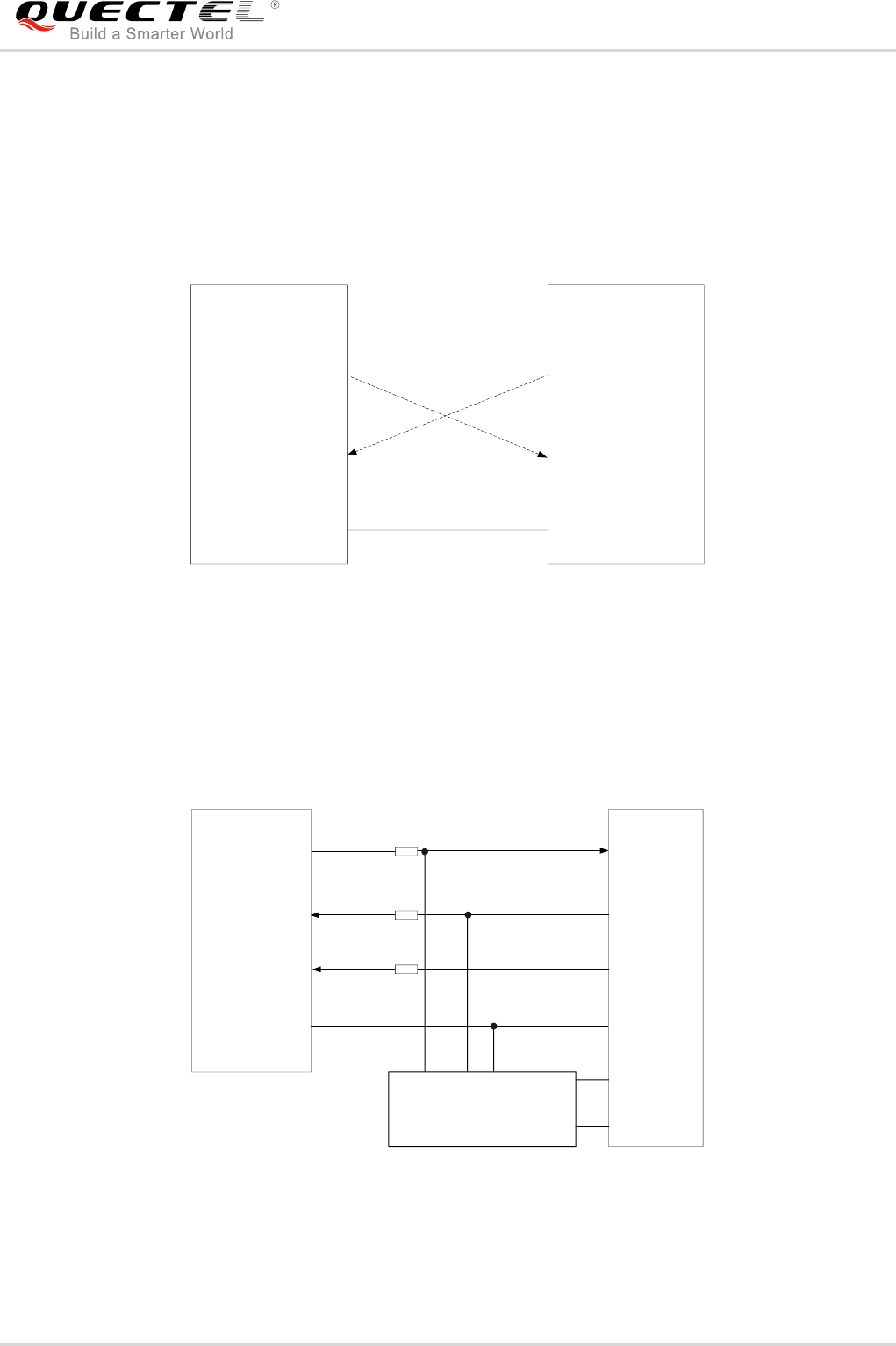
3.8.2. Debug Port
The debug port is used to view log information with the UEMonitor tool for firmware debugging, and the
baud rate is 921600bps. For detailed usage of the UEMonitor, please refer to document [3].
A reference design for debug port is shown as below.
DBG_TXD
DBG_RXD
DBG_TXD
DBG_RXD
Module (DCE)
Serial portDebug port
GND GND
PC (DTE)
Figure 10: Reference Design for Debug Port
3.8.3. UART Application
A reference design of 3.3V level match is shown as below.
Peripheral
TXD
RXD
1K
TXD
RXD
RI
EINT
Module
Voltage level: 3.3V
1K
1K
GND GND
TXD
RXD GND
Test points RESET
VBAT VBAT
RESET
Figure 11: Level Match Design for 3.3V System
NB-IoT Module Series
BC95-D Hardware Design Datasheet
BC95-D_Hardware_Design_Datasheet 27 / 55
1. In order to reduce the power consumption of the system, it is highly recommended to add a resistor
with resistance greater than 1KΩ on the UART port signal traces when the host’s voltage level is 3V or
3.3V.
2. It is recommended to reserve the test points (GND, RXD, TXD, VBAT and RESET) for firmware
upgrading.
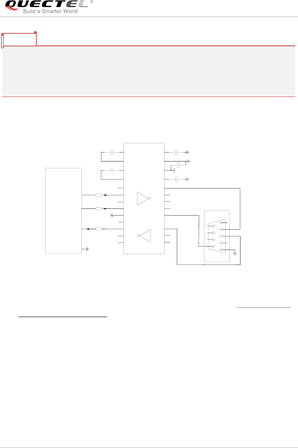
The following circuit shows a reference design for the communication between the module and PC. As the
voltage level of module is 3.0V, a RS-232 transceiver must be used. Please make sure the I/O voltage of
transceiver which connects to module is 3.0V.
TXD
RXD
RI
Module
GND
C1+
C1-
C2+
C2-
V+
VCC
GND
V-
3.3V
T1IN
T2IN
T3IN
T4IN
R1IN
R2IN
R3IN
R1OUT
R2OUT
R3OUT
T1OUT
T2OUT
T5OUT
T3OUT
T4OUT
T5IN
GND
GND
/R1OUT 1
2
3
4
5
7
8
9
GND
To PC Main Serial Port
GND
1K
1K
1K
RS-232 Transceiver
6
Figure 12: Sketch Map for RS-232 Interface Match
Please visit vendors’ web sites to select a suitable RS-232 transceiver IC, such as: http://www.exar.com
and http://www.maximintegrated.com.
3.9. USIM Interface
The module provides one USIM interface to allow the module to access an external USIM card.
The USIM interface supports the functionality of the 3GPP specification, and is intended for use with a
USIM application tool-kit.
The USIM card interface is powered by an internal regulator in the module. Both 1.8V and 3.0V USIM
cards are supported.
NOTES
NB-IoT Module Series
BC95-D Hardware Design Datasheet
BC95-D_Hardware_Design_Datasheet 28 / 55
Table 11: Pin Definition of the USIM Interface
A reference circuit for 6-pin USIM card connector is illustrated as the following figure.
Module
USIM_VDD
USIM_GND
USIM_RST
USIM_CLK
USIM_DATA 22R
22R
22R
100nF USIM Card Connector
GND
TVS
33pF33pF 33pF
VCC
RST
CLK IO
VPP
GND
GND
Figure 13: Reference Circuit for USIM Interface with 6-pin USIM Card Connector
For more information of USIM card connector, please visit http://www.amphenol.com and
http://www.molex.com.
In order to enhance the reliability and availability of the USIM card in application, please follow the criteria
below in USIM circuit design:
Keep placement of USIM card connector to the module as close as possible. Keep the trace length
as less than 200mm as possible.
Keep USIM card signals away from RF and VBAT traces.
Assure the ground between module and USIM card connector short and wide. Keep the trace width
of ground no less than 0.5mm to maintain the same electric potential. The decouple capacitor of
USIM_VDD is less than 1uF and must be near to USIM card connector.
Pin No.
Pin Name
Description
37
USIM_DETECT
USIM card plug in detect
38
USIM_VDD
Supply power for USIM card
USIM card voltage domain is 1.8V/3.0V±5%
41
USIM_CLK
USIM card clock signal
40
USIM_DATA
USIM card data signal
39
USIM_RST
USIM card reset signal
42
USIM_GND
Specified ground for USIM card

NB-IoT Module Series
BC95-D Hardware Design Datasheet
BC95-D_Hardware_Design_Datasheet 29 / 55
To avoid cross talk between USIM_DATA and USIM_CLK, keep them away from each other and
shield them with surrounded ground. USIM_RST should also be ground shielded.
In order to offer good ESD protection, it is recommended to add a TVS diode array. For more
information of TVS diode, please visit http://www.onsemi.com. The most important rule is to place the
ESD protection device close to the USIM card connector and make sure the USIM card interface
signal traces being protected will go through the ESD protection device first and then lead to the
module. The 22Ω resistors should be connected in series between the module and the USIM card
connector so as to suppress EMI spurious transmission and enhance ESD protection. Please note
that the USIM peripheral circuit should be close to the USIM card connector.
Place the RF bypass capacitors (33pF) close to the USIM card connector on all signals traces to
improve EMI suppression.
3.10. ADC Interface
The module provides a 10-bit ADC input channel to read the voltage value. This ADC interface is
available in both active and idle modes.
Table 12: Pin Definition of the ADC
Table 13: Characteristics of the ADC
Pin Name
Pin No.
Description
ADC
21
Analog to digital converter interface
Item
Min.
Typ.
Max.
Unit
Full-scale
Range (FSR)
Gain=0
1.45
V
Gain=1
2
V
Gain=2
2.5
V
Gain=3
3
V
Gain=4
3.5
V
Gain=5
4
V
Sampling Frequency
0
5
MHz
Input Impedance
100
MΩ

NB-IoT Module Series
BC95-D Hardware Design Datasheet
BC95-D_Hardware_Design_Datasheet 30 / 55
1)The overall accuracy is measured after calibration against internal reference.
3.11. DAC Interface
The module provides a 10-bit DAC output channel.
Table 14: Pin Definition of the DAC
Table 15: Characteristics of the DAC
Supply Current (from VBAT)
350
uA
INL
2
lsb
Offset
-10
10
mV
Overall Accuracy1)
-2.5
0
+2.5
%
Pin Name
Pin No.
Description
DAC
22
Digital to analog converter interface
Item
Min.
Typ.
Max.
Unit
LSB Voltage Step
Gain=0
1.2
mV
Gain=1
2.0
mV
Gain=2
2.8
mV
Gain=3
3.5
mV
LSB Voltage Step Accuracy
-4
4
%
Zero Crossing Offset (Nominal Output
at 0 Input)
-75
0
75
mV
Linearity, INL (VOUT > 20mV)
2
LSB
NOTE

NB-IoT Module Series
BC95-D Hardware Design Datasheet
BC95-D_Hardware_Design_Datasheet 31 / 55
3.12. SPI Interface
The module provides a serial peripheral interface (SPI).
Table 16: Pin Definition of the SPI
3.13. I2C Interface
The module provides an I2C interface.
Table 17: Pin Definition of the I2C
Linearity, DNL
2
LSB
Supply Current (at Zero Output Load)
100
150
uA
Output Current Capability
-1
1
mA
Output Driver Impedance (C load < 20pF)
1
Ω
Output Driver Impedance (Any C Load)
200
Ω
Maximum Signal Frequency
500
kHz
RMS Output Noise
0.5
LSB
Pin Name
Pin No.
Description
SPI_CS
10
SPI chip select
SPI_MISO
11
SPI master input
SPI_CLK
12
SPI clock
SPI_MOSI
13
SPI master output
Pin Name
Pin No.
Description
I2C_SCL
35
I2C clock
NB-IoT Module Series
BC95-D Hardware Design Datasheet
BC95-D_Hardware_Design_Datasheet 32 / 55
3.14. Behaviors of RI
When an SMS message is received or certain URCs are reported, RI pin will be triggered. The behaviors
of RI are shown as below.
Table 18: Behaviors of RI
HIGH
LOW
RI 120ms
Idle A URC or SMS message is received
Output message
Figure 14: Behaviors of RI when a URC or SMS Message is Received
Pleas pull down the RI pin for more than 120ms, the maximum time depends on the URC data output
length and the baud rate of the serial port.
I2C_SDA
36
I2C data
State
RI Response
Idle
HIGH
SMS
When an SMS message is received, the RI is changed to LOW and kept at low
level for about 120ms. Then it is changed to HIGH.
URC
Certain URCs can trigger RI to LOW for 120ms before the URC comes out. Then it
is changed to HIGH.
NOTE
NB-IoT Module Series
BC95-D Hardware Design Datasheet
BC95-D_Hardware_Design_Datasheet 33 / 55
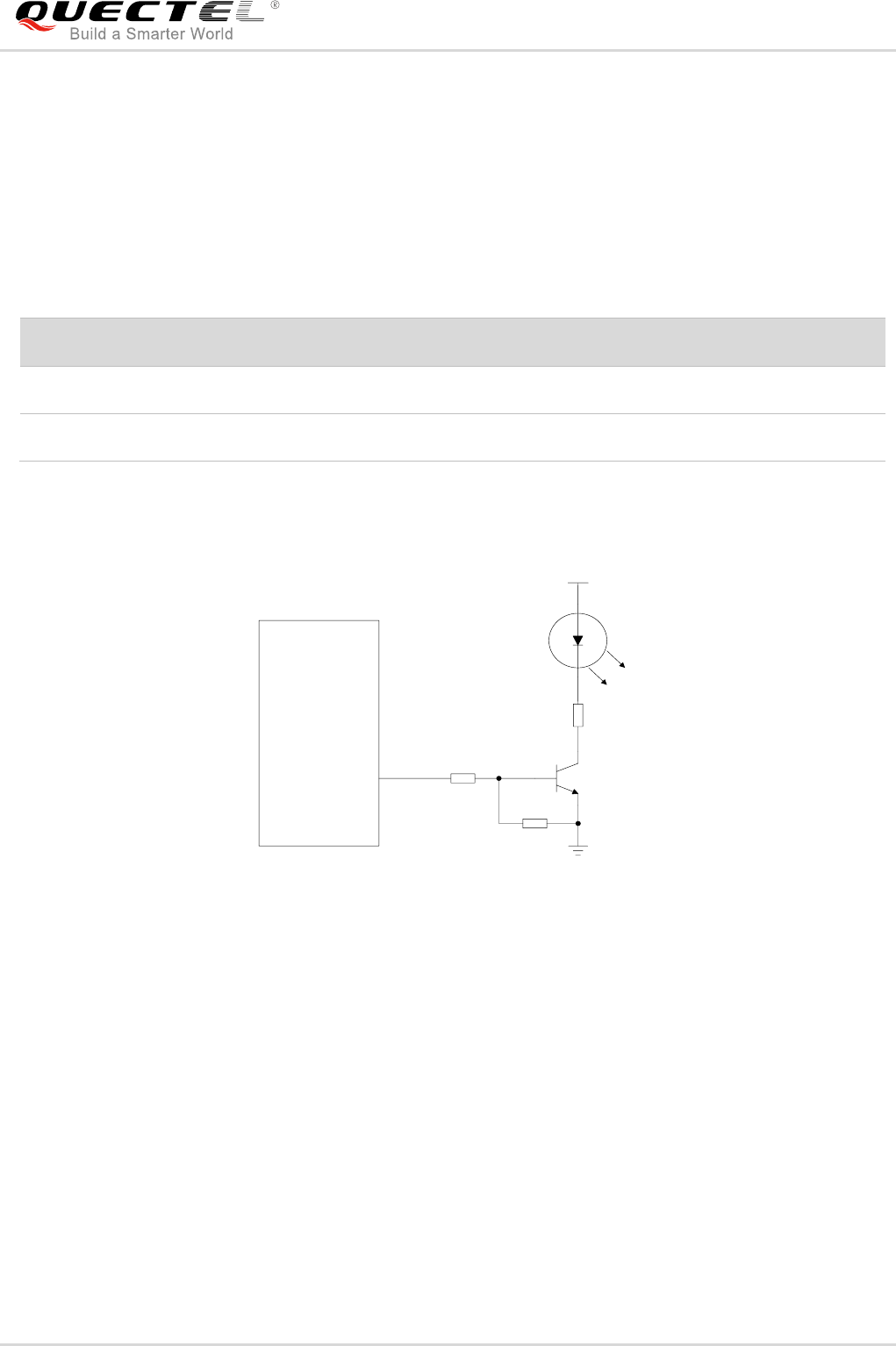
3.15. Network Status Indication
The NETLIGHT signal can be used to drive a network status indication LED. The working state of this pin
is listed in the following table.
Table 19: Working State of NETLIGHT
A reference circuit is shown as below.
Module
NETLIGHT 4.7K
47K
2.2K
VBAT
Figure 15: Reference Design for NETLIGHT
State
Module Function
Low (Light off)
The module is not working or not attached to network.
High (Light on)
The module is attached to network.
NB-IoT Module Series
BC95-D Hardware Design Datasheet
BC95-D_Hardware_Design_Datasheet 34 / 55
4 Antenna Interface
The pin 53 is the RF antenna pad. The impedance of the antenna port is 50Ω.
Table 20: Pin Definition of the RF Antenna Interface
4.1. RF Antenna Reference Design
A reference design for RF antenna is shown as below.
Module
RF_ANT
R1 0R
C1
NM
C2
NM
GND
GND
Figure 16: Reference Design for RF Antenna
BC95-D provides an RF antenna pad for antenna connection. There is a ground pad on each side of the
antenna pad in order to give a better grounding. Additionally, a π-type matching circuit is recommended to
be used to adjust the RF performance. Please place the π-type matching components (R1/C1/C2) as
close to the antenna as possible, and mount them according to actual needs. The capacitors (C1/C2) are
Pin Name
Pin No.
Description
GND
51
Ground
GND
52
Ground
RF_ANT
53
RF antenna pad
GND
54
Ground
NB-IoT Module Series
BC95-D Hardware Design Datasheet
BC95-D_Hardware_Design_Datasheet 35 / 55
not mounted and a 0Ω resistor is mounted on R1 by default.
4.2. Reference Design of RF Layout
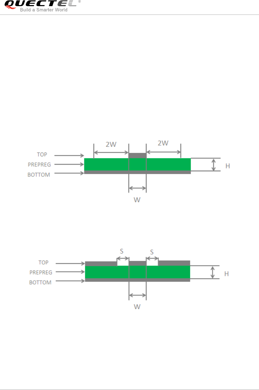
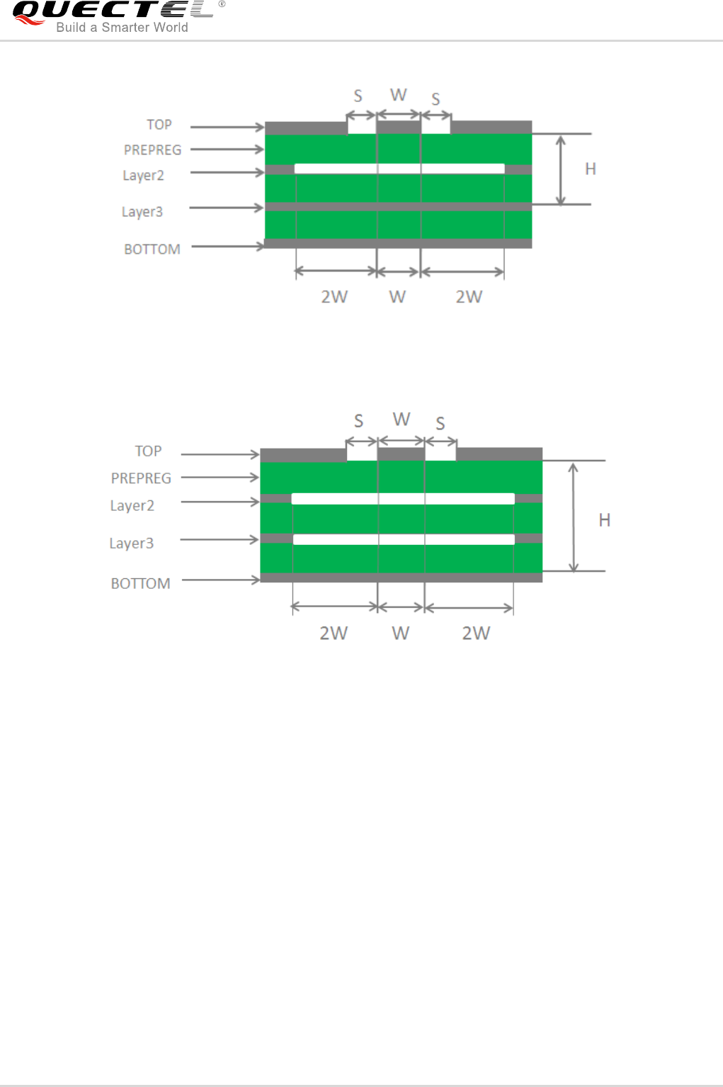
For user’s PCB, the characteristic impedance of all RF traces should be controlled as 50Ω±10%. The
impedance of the RF traces is usually determined by the trace width (W), the materials’ dielectric constant,
the distance between signal layer and reference ground (H), and the clearance between RF trace and
ground (S). Microstrip line or coplanar waveguide line is typically used in RF layout for characteristic
impedance control. The following are reference designs of microstrip line or coplanar waveguide line with
different PCB structures.
Figure 17: Microstrip Line Design on a 2-layer PCB
Figure 18: Coplanar Waveguide Line Design on a 2-layer PCB
NB-IoT Module Series
BC95-D Hardware Design Datasheet
BC95-D_Hardware_Design_Datasheet 36 / 55
Figure 19: Coplanar Waveguide Line Design on a 4-layer PCB (Layer 3 as Reference Ground)
Figure 20: Coplanar Waveguide Line Design on a 4-layer PCB (Layer 4 as Reference Ground)
In order to ensure RF performance and reliability, the following principles should be complied with in RF
layout design:
Use an impedance simulation tool to control the characteristic impedance of RF traces as 50Ω±10%.
The GND pins adjacent to RF pins should not be designed as thermal relief pads, and should be fully
connected to ground.
The distance between the RF pins and the RF connector should be as short as possible, and all the
right angle traces should be changed to curved ones.
There should be clearance area under the signal pin of the antenna connector or solder joint.
The reference ground of RF traces should be complete. Meanwhile, adding some ground vias around
RF traces and the reference ground could help to improve RF performance. The distance between
the ground vias and RF traces should be no less than two times the width of RF signal traces (2*W).
For more details about RF layout, please refer to document [5].
NB-IoT Module Series
BC95-D Hardware Design Datasheet
BC95-D_Hardware_Design_Datasheet 37 / 55
4.3. RF Output Power
Table 21: RF Output Power (Uplink QPSK and BPSK Modulation)
The design is compliant with the NB-IoT radio protocol 3GPP Rel.14.
4.4. RF Receiving Sensitivity
Table 22: RF Receiving Sensitivity (Throughput ≥ 95%)
The RF receiving sensitivity is tested under target BLER=10%, 1T1R, AWGN and MCS0 with Rep128.
4.5. Operating Frequencies
Table 23: Operating Frequencies
Frequency
Max.
Min.
1915MHz~1920MHz
23dBm±2dB
<-40dBm
Frequency
Receiving Sensitivity
722MHz~728MHz
-129dBm±2dB
1995MHz~2020MHz
-129dBm±2dB
Frequency Bands
Transmit
Receive
B111
1915MHz~1920MHz
722MHz~728MHz
NOTE
NOTE

NB-IoT Module Series
BC95-D Hardware Design Datasheet
BC95-D_Hardware_Design_Datasheet 38 / 55
4.6. Antenna Requirement
The following table shows the requirement on NB-IoT antenna.
Table 24: Antenna Requirement
4.7. Recommended RF Connector for Antenna Installation
If RF connector is used for antenna connection, it is recommended to use SMA-F connector.
B222
1915MHz~1920MHz
1995MHz~2020MHz
Type
Requirement
Frequency Range
720MHz~730MHz; 1915MHz~2020MHz
Max Input Power (W)
5
Input Impedance (Ω)
50
Polarization Type
Linear

NB-IoT Module Series
BC95-D Hardware Design Datasheet
BC95-D_Hardware_Design_Datasheet 39 / 55
5 Electrical, Reliability and Radio
Characteristics
5.1. Absolute Maximum Ratings
Absolute maximum ratings for power supply and voltage on digital and analog pins of the module are
listed in the following table.
Table 25: Absolute Maximum Ratings
5.2. Operation and Storage Temperatures
The operation and storage temperatures are listed in the following table.
Table 26: Operation and Storage Temperatures
Parameter
Min.
Max.
Unit
VBAT
-0.3
+4.25
V
Current of Power Supply
0
0.8
A
Voltage at Digital Pins
-0.3
+4.25
V
Voltage at Analog Pins
-0.3
+4.25
V
Voltage at Digital/Analog Pins in Power Down Mode
-0.25
+0.25
V
Parameter
Min.
Typ.
Max.
Unit
Operation Temperature Range1)
-40
+25
+85
ºC
NB-IoT Module Series
BC95-D Hardware Design Datasheet
BC95-D_Hardware_Design_Datasheet 40 / 55
1) Within operation temperature range, the module is 3GPP compliant.
5.3. Current Consumption
The values of current consumption are shown below.
Table 27: Current Consumption
5.4. Electrostatic Discharge
The module is not protected against electrostatic discharge (ESD) in general. Consequently, it is subject
to ESD handling precautions that typically apply to ESD sensitive components. Proper ESD handling and
packaging procedures must be applied throughout the processing, handling and operation of any
application that incorporates the module.
The following table shows the module’s electrostatic discharge characteristics.
Storage Temperature Range
-40
+90
ºC
Parameter
Description
Conditions
Min.
Typ.
Max.
Unit
IVBAT
PSM
Deep sleep state
3.6
5
uA
Idle mode
Standby state @DRX=1.28s
2
mA
Active mode
Radio transmission @23dBm
(Single-tone)
250
mA
Radio transmission @23dBm
(Multi-tone)
350
mA
Radio transmission @25dBm
(Single-tone)
350
mA
Radio reception
50
mA
NOTE

NB-IoT Module Series
BC95-D Hardware Design Datasheet
BC95-D_Hardware_Design_Datasheet 41 / 55
Table 28: Electrostatic Discharge Characteristics
Test Points
Contact Discharge
Air Discharge
Unit
VBAT, GND
±5
±10
kV
Antenna Interface
±5
±10
kV
Other Interfaces
±0.5
±1
kV
NB-IoT Module Series
BC95-D Hardware Design Datasheet
BC95-D_Hardware_Design_Datasheet 42 / 55
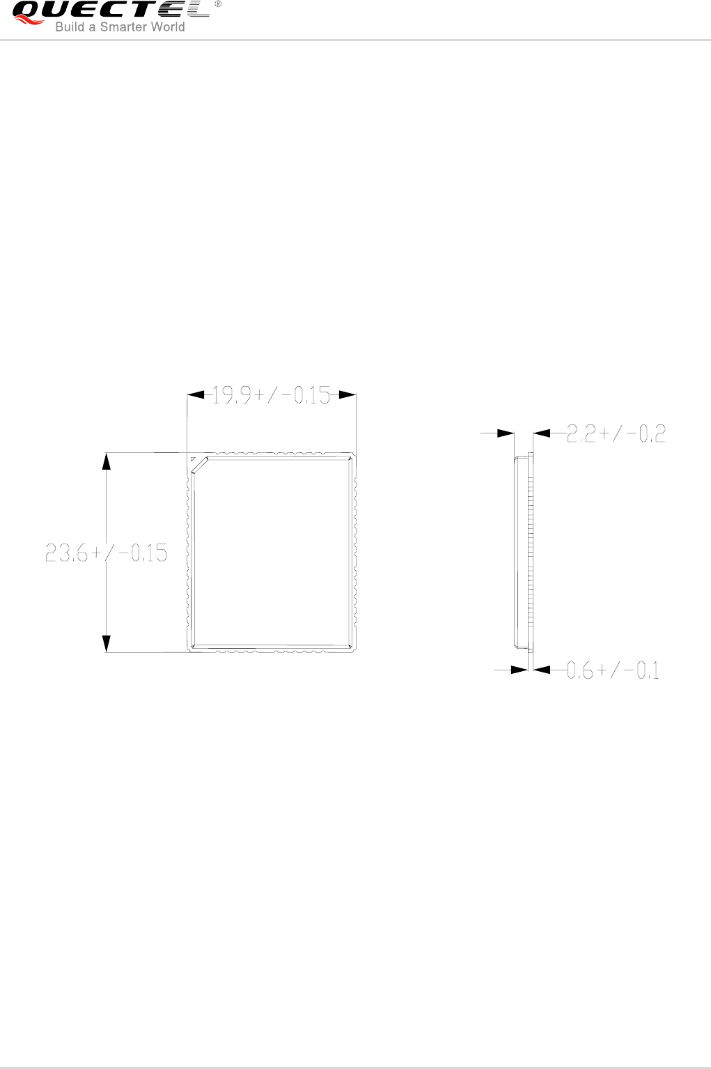
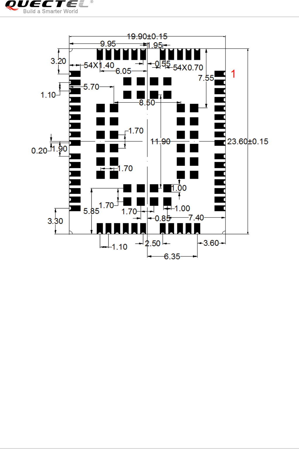
6 Mechanical Dimensions
This chapter describes the mechanical dimensions of the module. All dimensions are measured in mm.
The tolerances for dimensions without tolerance values are ±0.05mm.
6.1. Mechanical Dimensions of the Module
Figure 21: Module Top and Side Dimensions
NB-IoT Module Series
BC95-D Hardware Design Datasheet
BC95-D_Hardware_Design_Datasheet 43 / 55
Figure 22: Module Bottom Dimensions (Bottom View)
NB-IoT Module Series
BC95-D Hardware Design Datasheet
BC95-D_Hardware_Design_Datasheet 44 / 55
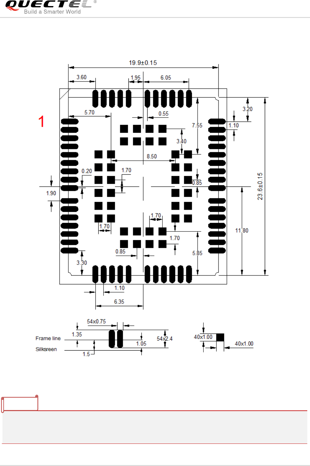
6.2. Recommended Footprint
Figure 23: Recommended Footprint (Top View)
1. For easy maintenance of the module, please keep about 3mm between the module and other
components in the host PCB.
2. All RESERVED pins must not be connected to GND.
NOTES
NB-IoT Module Series
BC95-D Hardware Design Datasheet
BC95-D_Hardware_Design_Datasheet 45 / 55
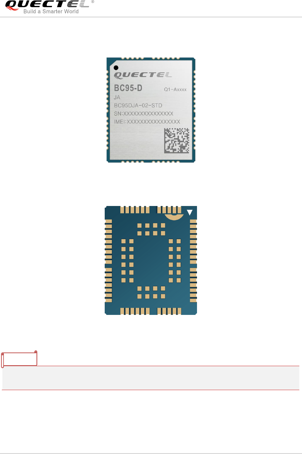
6.3. Design Effect Drawings of the Module
Figure 24: Top View of the Module
Figure 25: Bottom View of the Module
These are design effect drawings of BC95-D module. For more accurate pictures, please refer to the
module that you get from Quectel.
NOTE
NB-IoT Module Series
BC95-D Hardware Design Datasheet
BC95-D_Hardware_Design_Datasheet 46 / 55
7 Storage, Manufacturing and
Packaging
7.1. Storage
BC95-D module is stored in a vacuum-sealed bag. It is rated at MSL 3, and its storage restrictions are
shown as below.
1. Shelf life in the vacuum-sealed bag: 12 months at <40ºC /90%RH.
2. After the vacuum-sealed bag is opened, devices that will be subjected to reflow soldering or other
high temperature processes must be:
Mounted within 168 hours at the factory environment of ≤30ºC /60% RH.
Stored at <10% RH.
3. Devices require baking before mounting, if any circumstance below occurs:
When the ambient temperature is 23ºC ±5 ºC and the humidity indication card shows the humidity
is >10% before opening the vacuum-sealed bag.
Device mounting cannot be finished within 168 hours at factory conditions of ≤30ºC /60%
4. If baking is required, devices may be baked for 8 hours at 120ºC ±5 ºC .
As the plastic package cannot be subjected to high temperature, it should be removed from devices
before high temperature (120ºC ) baking. If shorter baking time is desired, please refer to the
IPC/JEDECJ-STD-033 for baking procedure.
NOTE
NB-IoT Module Series
BC95-D Hardware Design Datasheet
BC95-D_Hardware_Design_Datasheet 47 / 55
7.2. Manufacturing and Soldering
Push the squeegee to apply the solder paste on the surface of stencil, thus making the paste fill the
stencil openings and then penetrate to the PCB. The force on the squeegee should be adjusted properly
so as to produce a clean stencil surface on a single pass. To ensure the module soldering quality, the
thickness of stencil for the module is recommended to be 0.15mm. For more details, please refer to
document [4].
It is suggested that the peak reflow temperature is 235ºC ~245ºC (for SnAg3.0Cu0.5 alloy). The absolute
max reflow temperature is 260ºC. To avoid damage to the module caused by repeatedly heating, it is
suggested that the module should be mounted after reflow soldering for the other side of PCB has been
completed. Recommended reflow soldering thermal profile is shown below.
Time
50 100 150 200 250 300
50
100
150
200
250
160ºC
200ºC
217
0
70s~120s
40s~60s
Between 1~3ºC/s
Preheat Heating Cooling
ºC
s
Liquids Temperature
Temperature
Figure 26: Reflow Soldering Thermal Profile
1. During manufacturing and soldering, or any other processes that may contact the module directly,
NEVER wipe the module’s shielding can with organic solvents, such as acetone, ethyl alcohol,
isopropyl alcohol, trichloroethylene, etc. Otherwise, the shielding can may become rusted.
NOTES
NB-IoT Module Series
BC95-D Hardware Design Datasheet
BC95-D_Hardware_Design_Datasheet 48 / 55
2. The shielding can for the module is made of Cupro-Nickel base material. It is tested that after 12
hours’ Neutral Salt Spray test, the laser engraved label information on the shielding can is still clearly
identifiable and the QR code is still readable, although white rust may be found.
7.3. Packaging
The modules are stored inside a vacuum-sealed bag which is ESD protected. It should not be opened
until the devices are ready to be soldered onto the application.
7.3.1. Tape and Reel Packaging
The reel is 330mm in diameter and each reel contains 250 modules.
Figure 27: Tape Dimensions
NB-IoT Module Series
BC95-D Hardware Design Datasheet
BC95-D_Hardware_Design_Datasheet 49 / 55
PS
6
DETAIL:A
DETAIL:A
Figure 28: Reel Dimensions

NB-IoT Module Series
BC95-D Hardware Design Datasheet
BC95-D_Hardware_Design_Datasheet 50 / 55
8 Appendix A References
Table 29: Related Documents
Table 30: Terms and Abbreviations
SN
Document Name
Remark
[1]
Quectel_BC95-D_AT_Commands_Manual
BC95-D AT Commands Manual
[2]
Quectel_BC95-D_Firmware_Upgrade_User_Guide
BC95-D Firmware Upgrade User Guide
[3]
Quectel_BC95-D_UEMonitor_User_Guide
BC95-D UEMonitor User Guide
[4]
Quectel_Module_Secondary_SMT_User_Guide
Module Secondary SMT User Guide
[5]
Quectel_RF_Layout_Application_Note
RF Layout Application Note
[6]
NL-002871-SP-2C-Hi2115 C30 Datasheet
Datasheet on which this document is
based
[7]
Quectel_BC95-D_Reference_Design
BC95-D Reference Design
Abbreviation
Description
ADC
Analog-to-Digital Converter
AS
Access Stratum
DAC
Digital-to-Analog Converter
DCE
Data Communications Equipment (typically module)
DNL
Differential Nonlinearity
DTE
Data Terminal Equipment (typically computer, external controller)
DRX
Discontinuous Reception
H-FDD
Half Frequency Division Duplexing

NB-IoT Module Series
BC95-D Hardware Design Datasheet
BC95-D_Hardware_Design_Datasheet 51 / 55
I/O
Input/Output
IC
Integrated Circuit
Imax
Maximum Load Current
INL
Integral Nonlinearity
Inorm
Normal Current
kbps
Kilo Bits Per Second
LED
Light Emitting Diode
LPUART
Low Power Universal Asynchronous Receiver/Transmitter
LSB
Least Significant Bit
MME
Mobility Management Entity
MO
Mobile Originated
NB-IoT
Narrow Band Internet of Things
PCB
Printed Circuit Board
PDN
Public Data Network
PSM
Power Saving Mode
RF
Radio Frequency
RoHS
Restriction of Hazardous Substances
RTC
Real Time Clock
RX
Receive Direction
USIM
Universal Subscriber Identification Module
SMS
Short Message Service
TAU
Tracking Area Update
TE
Terminal Equipment
TX
Transmitting Direction
UART
Universal Asynchronous Receiver & Transmitter

NB-IoT Module Series
BC95-D Hardware Design Datasheet
BC95-D_Hardware_Design_Datasheet 52 / 55
URC
Unsolicited Result Code
VSWR
Voltage Standing Wave Ratio
Vmax
Maximum Voltage Value
Vnorm
Normal Voltage Value
Vmin
Minimum Voltage Value
VIHmax
Maximum Input High Level Voltage Value
VIHmin
Minimum Input High Level Voltage Value
VILmax
Maximum Input Low Level Voltage Value
VILmin
Minimum Input Low Level Voltage Value
VImax
Absolute Maximum Input Voltage Value
VImin
Absolute Minimum Input Voltage Value
VOHmax
Maximum Output High Level Voltage Value
VOHmin
Minimum Output High Level Voltage Value
VOLmax
Maximum Output Low Level Voltage Value
VOLmin
Minimum Output Low Level Voltage Value

NB-IoT Module Series
BC95-D Hardware Design Datasheet
BC95-D_Hardware_Design_Datasheet 53 / 55
FCC Certification Requirements.
According to the definition of mobile and fixed device is described in Part 2.1091(b), this device is a
mobile device.
And the following conditions must be met:
1. This Modular Approval is limited to OEM installation for mobile and fixed applications only. The antenna
installation and operating configurations of this transmitter, including any applicable source-based time-
averaging duty factor, antenna gain and cable loss must satisfy MPE categorical Exclusion Requirements
of 2.1091.
2. The EUT is a mobile device; maintain at least a 20 cm separation between the EUT and the user’s body
and must not transmit simultaneously with any other antenna or transmitter.
3.A label with the following statements must be attached to the host end product: This device contains
FCC ID: XMR201807BC95D.
4.To comply with FCC regulations limiting both maximum RF output power and human exposure to RF
radiation, maximum antenna gain (including cable loss) must not exceed:
❒ Band111(Tx: 1915MHz~1920MHz): <4dBi
❒ Band222(Tx: 1915MHz~1920MHz): <4dBi
5. This module must not transmit simultaneously with any other antenna or transmitter
6. The host end product must include a user manual that clearly defines operating requirements and
conditions that must be observed to ensure compliance with current FCC RF exposure guidelines.
For portable devices, in addition to the conditions 3 through 6 described above, a separate approval is
required to satisfy the SAR requirements of FCC Part 2.1093
If the device is used for other equipment that separate approval is required for all other operating
configurations, including portable configurations with respect to 2.1093 and different antenna
configurations.

NB-IoT Module Series
BC95-D Hardware Design Datasheet
BC95-D_Hardware_Design_Datasheet 54 / 55
For this device, OEM integrators must be provided with labeling instructions of finished products.
Please refer to KDB784748 D01 v07, section 8. Page 6/7 last two paragraphs:
A certified modular has the option to use a permanently affixed label, or an electronic label. For a
permanently affixed label, the module must be labeled with an FCC ID - Section 2.926 (see 2.2
Certification (labeling requirements) above). The OEM manual must provide clear instructions
explaining to the OEM the labeling requirements, options and OEM user manual instructions that are
required (see next paragraph).
For a host using a certified modular with a standard fixed label, if (1) the module’s FCC ID is not visible
when installed in the host, or (2) if the host is marketed so that end users do not have straightforward
commonly used methods for access to remove the module so that the FCC ID of the module is visible;
then an additional permanent label referring to the enclosed module: “Contains Transmitter Module
FCC ID: XMR201807BC95D” or “Contains FCC ID: XMR201807BC95D” must be used. The host OEM
user manual must also contain clear instructions on how end users can find and/or access the module
and the FCC ID.
The final host / module combination may also need to be evaluated against the FCC Part 15B criteria
for unintentional radiators in order to be properly authorized for operation as a Part 15 digital device.
The user’s manual or instruction manual for an intentional or unintentional radiator shall caution the
user that changes or modifications not expressly approved by the party responsible for compliance
could void the user's authority to operate the equipment. In cases where the manual is provided only in
a form other than paper, such as on a computer disk or over the Internet, the information required by
this section may be included in the manual in that alternative form, provided the user can reasonably be
expected to have the capability to access information in that form.
This device complies with part 15 of the FCC Rules. Operation is subject to the following two conditions:
(1) This device may not cause harmful interference, and (2) this device must accept any interference
received, including interference that may cause undesired operation.
Changes or modifications not expressly approved by the manufacturer could void the user’s authority to

NB-IoT Module Series
BC95-D Hardware Design Datasheet
BC95-D_Hardware_Design_Datasheet 55 / 55
operate the equipment.
To ensure compliance with all non-transmitter functions the host manufacturer is responsible for ensuring
compliance with the module(s) installed and fully operational. For example, if a host was previously
authorized as an unintentional radiator under the Declaration of Conformity procedure without a
transmitter certified module and a module is added, the host manufacturer is responsible for ensuring that
the after the module is installed and operational the host continues to be compliant with the Part 15B
unintentional radiator requirements.