Quectel Wireless Solutions 201807EG95NA LTE Module User Manual
Quectel Wireless Solutions Company Limited LTE Module Users Manual
Users Manual


LTE Module Series
EG95 Hardware Design
EG95_Hardware_Design 1 / 81
Our aim is to provide customers with timely and comprehensive service. For any
assistance, please contact our company headquarters:
Quectel Wireless Solutions Co., Ltd.
7th Floor, Hongye Building, No.1801 Hongmei Road, Xuhui District, Shanghai 200233, China
Tel: +86 21 5108 6236
Email: info@quectel.com
Or our local office. For more information, please visit:
http://quectel.com/support/sales.htm
For technical support, or to report documentation errors, please visit:
http://quectel.com/support/technical.htm
Or email to: support@quectel.com
GENERAL NOTES
QUECTEL OFFERS THE INFORMATION AS A SERVICE TO ITS CUSTOMERS. THE INFORMATION
PROVIDED IS BASED UPON CUSTOMERS’ REQUIREMENTS. QUECTEL MAKES EVERY EFFORT
TO ENSURE THE QUALITY OF THE INFORMATION IT MAKES AVAILABLE. QUECTEL DOES NOT
MAKE ANY WARRANTY AS TO THE INFORMATION CONTAINED HEREIN, AND DOES NOT ACCEPT
ANY LIABILITY FOR ANY INJURY, LOSS OR DAMAGE OF ANY KIND INCURRED BY USE OF OR
RELIANCE UPON THE INFORMATION. ALL INFORMATION SUPPLIED HEREIN IS SUBJECT TO
CHANGE WITHOUT PRIOR NOTICE.
COPYRIGHT
THE INFORMATION CONTAINED HERE IS PROPRIETARY TECHNICAL INFORMATION OF
QUECTEL WIRELESS SOLUTIONS CO., LTD. TRANSMITTING, REPRODUCTION, DISSEMINATION
AND EDITING OF THIS DOCUMENT AS WELL AS UTILIZATION OF THE CONTENT ARE
FORBIDDEN WITHOUT PERMISSION. OFFENDERS WILL BE HELD LIABLE FOR PAYMENT OF
DAMAGES. ALL RIGHTS ARE RESERVED IN THE EVENT OF A PATENT GRANT OR
REGISTRATION OF A UTILITY MODEL OR DESIGN.
Copyright © Quectel Wireless Solutions Co., Ltd. 2018. All rights reserved.

LTE Module Series
EG95 Hardware Design
EG95_Hardware_Design 2 / 81
About the Document
History
Revision
Date
Author
Description
1.0
2017-03-22
Felix YIN/
Yeoman CHEN/
Jackie WANG
Initial
1.1
2018-01-04
Yeoman CHEN/
Rex WANG
1. Added band B28A.
2. Updated the description of UMTS and GSM
features in Table 2.
3. Updated the functional diagram in Figure 1.
4. Updated module operating frequencies in
Table 21.
5. Updated current consumption in Table 26.
6. Updated the conducted RF receiving
sensitivity in Table 28.
7. Updated the GPRS multi-slot classes in
Table 33.
8. Added thermal consideration in Chapter 5.8
9. Added a GND pad in each of the four corners
of the module’s footprint in Chapter 6.2.
10. Added packaging information in Chapter 7.3.
1.2
2018-03-14
Felix YIN/
Rex WANG
1. Added the description of EG95-NA.
2. Updated the functional diagram in Figure 1.
3. Updated pin assignment in Figure 2.
4. Updated GNSS function in Table 1.
5. Updated GNSS Features in Table 2.
6. Updated reference circuit of USB interface
in Figure 21.
7. Added description of GNSS receiver in
Chapter 4.
8. Updated pin definition of RF antenna in
Table 21.

LTE Module Series
EG95 Hardware Design
EG95_Hardware_Design 3 / 81
9. Updated module operating frequencies in
Table 22.
10. Added description of GNSS antenna
interface in Chapter 5.2.
11. Updated antenna requirements in Table 25.
12. Updated RF output power in Table 32.

LTE Module Series
EG95 Hardware Design
EG95_Hardware_Design 4 / 81
Contents
About the Document ................................................................................................................................... 2
Contents ....................................................................................................................................................... 4
Table Index ................................................................................................................................................... 6
Figure Index ................................................................................................................................................. 7
1 Introduction .......................................................................................................................................... 9
1.1. Safety Information.................................................................................................................... 10
2 Product Concept ................................................................................................................................ 11
2.1. General Description ................................................................................................................. 11
2.2. Key Features ........................................................................................................................... 12
2.3. Functional Diagram ................................................................................................................. 14
2.4. Evaluation Board ..................................................................................................................... 15
3 Application Interfaces ....................................................................................................................... 16
3.1. General Description ................................................................................................................. 16
3.2. Pin Assignment ........................................................................................................................ 17
3.3. Pin Description ......................................................................................................................... 18
3.4. Operating Modes ..................................................................................................................... 24
3.5. Power Saving ........................................................................................................................... 24
3.5.1. Sleep Mode .................................................................................................................... 24
3.5.1.1. UART Application ................................................................................................. 25
3.5.1.2. USB Application with USB Remote Wakeup Function ........................................ 25
3.5.1.3. USB Application with USB Suspend/Resume and RI Function .......................... 26
3.5.1.4. USB Application without USB Suspend Function ................................................ 27
3.5.2. Airplane Mode ................................................................................................................ 27
3.6. Power Supply ........................................................................................................................... 28
3.6.1. Power Supply Pins ......................................................................................................... 28
3.6.2. Decrease Voltage Drop .................................................................................................. 29
3.6.3. Reference Design for Power Supply .............................................................................. 30
3.6.4. Monitor the Power Supply .............................................................................................. 30
3.7. Turn on and off Scenarios ....................................................................................................... 30
3.7.1. Turn on Module Using the PWRKEY ............................................................................. 30
3.7.2. Turn off Module .............................................................................................................. 32
3.7.2.1. Turn off Module Using the PWRKEY Pin ............................................................. 32
3.7.2.2. Turn off Module Using AT Command ................................................................... 33
3.8. Reset the Module..................................................................................................................... 33
3.9. (U)SIM Interfaces..................................................................................................................... 35
3.10. USB Interface .......................................................................................................................... 38
3.11. UART Interfaces ...................................................................................................................... 40
3.12. PCM and I2C Interfaces .......................................................................................................... 42
3.13. SPI Interface ............................................................................................................................ 45
3.14. Network Status Indication ........................................................................................................ 45

LTE Module Series
EG95 Hardware Design
EG95_Hardware_Design 5 / 81
3.15. STATUS ................................................................................................................................... 46
3.16. Behaviors of RI ........................................................................................................................ 47
4 GNSS Receiver ................................................................................................................................... 48
4.1. General Description ................................................................................................................. 48
4.2. GNSS Performance ................................................................................................................. 48
4.3. Layout Guidelines .................................................................................................................... 49
5 Antenna Interfaces ............................................................................................................................. 50
5.1. Main/Rx-diversity Antenna Interfaces...................................................................................... 50
5.1.1. Pin Definition .................................................................................................................. 50
5.1.2. Operating Frequency ..................................................................................................... 50
5.1.3. Reference Design of RF Antenna Interface ................................................................... 51
5.1.4. Reference Design of RF Layout..................................................................................... 52
5.2. GNSS Antenna Interface ......................................................................................................... 54
5.3. Antenna Installation ................................................................................................................. 55
5.3.1. Antenna Requirement .................................................................................................... 55
5.3.2. Recommended RF Connector for Antenna Installation ................................................. 56
6 Electrical, Reliability and Radio Characteristics ............................................................................ 58
6.1. Absolute Maximum Ratings ..................................................................................................... 58
6.2. Power Supply Ratings ............................................................................................................. 58
6.3. Operation and Storage Temperatures ..................................................................................... 59
6.4. Current Consumption .............................................................................................................. 60
6.5. RF Output Power ..................................................................................................................... 63
6.6. RF Receiving Sensitivity .......................................................................................................... 64
6.7. Electrostatic Discharge ............................................................................................................ 65
6.8. Thermal Consideration ............................................................................................................ 66
7 Mechanical Dimensions .................................................................................................................... 68
7.1. Mechanical Dimensions of the Module.................................................................................... 68
7.2. Recommended Footprint ......................................................................................................... 70
7.3. Design Effect Drawings of the Module .................................................................................... 71
8 Storage, Manufacturing and Packaging .......................................................................................... 72
8.1. Storage .................................................................................................................................... 72
8.2. Manufacturing and Soldering .................................................................................................. 73
8.3. Packaging ................................................................................................................................ 74
9 Appendix A References ..................................................................................................................... 75
10 Appendix B GPRS Coding Schemes ............................................................................................... 78
11 Appendix C GPRS Multi-slot Classes .............................................................................................. 79
12 Appendix D EDGE Modulation and Coding Schemes ................................................................... 81

LTE Module Series
EG95 Hardware Design
EG95_Hardware_Design 6 / 81
Table Index
TABLE 1: FREQUENCY BANDS OF EG95 MODULE ....................................................................................... 11
TABLE 2: KEY FEATURES OF EG95 MODULE ............................................................................................... 12
TABLE 3: IO PARAMETERS DEFINITION ........................................................................................................ 18
TABLE 4: PIN DESCRIPTION ........................................................................................................................... 18
TABLE 5: OVERVIEW OF OPERATING MODES ............................................................................................. 24
TABLE 6: VBAT AND GND PINS ....................................................................................................................... 28
TABLE 7: PIN DEFINITION OF PWRKEY ........................................................................................................ 31
TABLE 8: PIN DEFINITION OF RESET_N ....................................................................................................... 33
TABLE 9: PIN DEFINITION OF (U)SIM INTERFACES ..................................................................................... 35
TABLE 10: PIN DEFINITION OF USB INTERFACE ......................................................................................... 38
TABLE 11: PIN DEFINITION OF MAIN UART INTERFACE ............................................................................. 40
TABLE 12: PIN DEFINITION OF DEBUG UART INTERFACE ......................................................................... 40
TABLE 13: LOGIC LEVELS OF DIGITAL I/O .................................................................................................... 41
TABLE 14: PIN DEFINITION OF PCM AND I2C INTERFACES ....................................................................... 44
TABLE 15: PIN DEFINITION OF SPI INTERFACE ........................................................................................... 45
TABLE 16: PIN DEFINITION OF NETWORK STATUS INDICATOR ................................................................ 46
TABLE 17: WORKING STATE OF THE NETWORK STATUS INDICATOR ...................................................... 46
TABLE 18: PIN DEFINITION OF STATUS ........................................................................................................ 46
TABLE 19: DEFAULT BEHAVIORS OF RI ........................................................................................................ 47
TABLE 20: GNSS PERFORMANCE ................................................................................................................. 48
TABLE 21: PIN DEFINITION OF RF ANTENNA ............................................................................................... 50
TABLE 22: MODULE OPERATING FREQUENCIES ........................................................................................ 50
TABLE 23: PIN DEFINITION OF GNSS ANTENNA INTERFACE .................................................................... 54
TABLE 24: GNSS FREQUENCY ...................................................................................................................... 54
TABLE 25: ANTENNA REQUIREMENTS .......................................................................................................... 55
TABLE 26: ABSOLUTE MAXIMUM RATINGS .................................................................................................. 58
TABLE 27: POWER SUPPLY RATINGS ........................................................................................................... 58
TABLE 28: OPERATION AND STORAGE TEMPERATURES .......................................................................... 59
TABLE 29: EG95-E CURRENT CONSUMPTION ............................................................................................. 60
TABLE 30: EG95-NA CURRENT CONSUMPTION........................................................................................... 62
TABLE 31: GNSS CURRENT CONSUMPTION OF EG95-NA ......................................................................... 63
TABLE 32: RF OUTPUT POWER ..................................................................................................................... 63
TABLE 33: EG95-E CONDUCTED RF RECEIVING SENSITIVITY .................................................................. 64
TABLE 34: EG95-NA CONDUCTED RF RECEIVING SENSITIVITY ............................................................... 65
TABLE 35: ELECTROSTATIC DISCHARGE CHARACTERISTICS ................................................................. 65
TABLE 36: RELATED DOCUMENTS ................................................................................................................ 75
TABLE 37: TERMS AND ABBREVIATIONS ...................................................................................................... 75
TABLE 38: DESCRIPTION OF DIFFERENT CODING SCHEMES .................................................................. 78
TABLE 39: GPRS MULTI-SLOT CLASSES ...................................................................................................... 79
TABLE 40: EDGE MODULATION AND CODING SCHEMES ........................................................................... 81

LTE Module Series
EG95 Hardware Design
EG95_Hardware_Design 7 / 81
Figure Index
FIGURE 1: FUNCTIONAL DIAGRAM ............................................................................................................... 15
FIGURE 2: PIN ASSIGNMENT (TOP VIEW)..................................................................................................... 17
FIGURE 3: SLEEP MODE APPLICATION VIA UART ....................................................................................... 25
FIGURE 4: SLEEP MODE APPLICATION WITH USB REMOTE WAKEUP .................................................... 26
FIGURE 5: SLEEP MODE APPLICATION WITH RI ......................................................................................... 26
FIGURE 6: SLEEP MODE APPLICATION WITHOUT SUSPEND FUNCTION ................................................ 27
FIGURE 7: POWER SUPPLY LIMITS DURING BURST TRANSMISSION ...................................................... 29
FIGURE 8: STAR STRUCTURE OF THE POWER SUPPLY............................................................................ 29
FIGURE 9: REFERENCE CIRCUIT OF POWER SUPPLY .............................................................................. 30
FIGURE 10: TURN ON THE MODULE USING DRIVING CIRCUIT ................................................................. 31
FIGURE 11: TURN ON THE MODULE USING BUTTON ................................................................................. 31
FIGURE 12: TIMING OF TURNING ON MODULE ........................................................................................... 32
FIGURE 13: TIMING OF TURNING OFF MODULE ......................................................................................... 33
FIGURE 14: REFERENCE CIRCUIT OF RESET_N BY USING DRIVING CIRCUIT ...................................... 34
FIGURE 15: REFERENCE CIRCUIT OF RESET_N BY USING BUTTON ...................................................... 34
FIGURE 16: TIMING OF RESETTING MODULE ............................................................................................. 34
FIGURE 17: REFERENCE CIRCUIT OF (U)SIM1 INTERFACE WITH AN 8-PIN (U)SIM CARD CONNECTOR
................................................................................................................................................................... 36
FIGURE 18: REFERENCE CIRCUIT OF (U)SIM1 INTERFACE WITH A 6-PIN (U)SIM CARD CONNECTOR 36
FIGURE 19: REFERENCE CIRCUIT OF (U)SIM2 INTERFACE WITH AN 8-PIN (U)SIM CARD CONNECTOR
................................................................................................................................................................... 37
FIGURE 20: REFERENCE CIRCUIT OF (U)SIM2 INTERFACE WITH A 6-PIN (U)SIM CARD CONNECTOR 37
FIGURE 21: REFERENCE CIRCUIT OF USB INTERFACE ............................................................................ 39
FIGURE 22: REFERENCE CIRCUIT WITH TRANSLATOR CHIP ................................................................... 41
FIGURE 23: REFERENCE CIRCUIT WITH TRANSISTOR CIRCUIT .............................................................. 42
FIGURE 24: PRIMARY MODE TIMING ............................................................................................................ 43
FIGURE 25: AUXILIARY MODE TIMING .......................................................................................................... 43
FIGURE 26: REFERENCE CIRCUIT OF PCM APPLICATION WITH AUDIO CODEC .................................... 44
FIGURE 27: REFERENCE CIRCUIT OF SPI INTERFACE WITH PERIPHERALS ......................................... 45
FIGURE 28: REFERENCE CIRCUIT OF THE NETWORK STATUS INDICATOR ........................................... 46
FIGURE 29: REFERENCE CIRCUIT OF STATUS ........................................................................................... 47
FIGURE 30: REFERENCE CIRCUIT OF RF ANTENNA INTERFACE ............................................................. 51
FIGURE 31: MICROSTRIP LINE DESIGN ON A 2-LAYER PCB ...................................................................... 52
FIGURE 32: COPLANAR WAVEGUIDE LINE DESIGN ON A 2-LAYER PCB .................................................. 52
FIGURE 33: COPLANAR WAVEGUIDE LINE DESIGN ON A 4-LAYER PCB (LAYER 3 AS REFERENCE
GROUND) .................................................................................................................................................. 53
FIGURE 34: COPLANAR WAVEGUIDE LINE DESIGN ON A 4-LAYER PCB (LAYER 4 AS REFERENCE
GROUND) .................................................................................................................................................. 53
FIGURE 35: REFERENCE CIRCUIT OF GNSS ANTENNA............................................................................. 54
FIGURE 36: DIMENSIONS OF THE U.FL-R-SMT CONNECTOR (UNIT: MM) ................................................ 56
FIGURE 37: MECHANICALS OF U.FL-LP CONNECTORS ............................................................................. 56

LTE Module Series
EG95 Hardware Design
EG95_Hardware_Design 8 / 81
FIGURE 38: SPACE FACTOR OF MATED CONNECTOR (UNIT: MM) ........................................................... 57
FIGURE 39: REFERENCED HEATSINK DESIGN (HEATSINK AT THE TOP OF THE MODULE) .................. 66
FIGURE 40: REFERENCED HEATSINK DESIGN (HEATSINK AT THE BOTTOM OF CUSTOMERS’ PCB) . 67
FIGURE 41: MODULE TOP AND SIDE DIMENSIONS ..................................................................................... 68
FIGURE 42: MODULE BOTTOM DIMENSIONS (TOP VIEW) ......................................................................... 69
FIGURE 43: RECOMMENDED FOOTPRINT (TOP VIEW) .............................................................................. 70
FIGURE 44: TOP VIEW OF THE MODULE ...................................................................................................... 71
FIGURE 45: BOTTOM VIEW OF THE MODULE .............................................................................................. 71
FIGURE 46: REFLOW SOLDERING THERMAL PROFILE .............................................................................. 73
FIGURE 47: TAPE DIMENSIONS ..................................................................................................................... 74
FIGURE 48: REEL DIMENSIONS ..................................................................................................................... 74

LTE Module Series
EG95 Hardware Design
EG95_Hardware_Design 9 / 81
1 Introduction
This document defines the EG95 module and describes its air interface and hardware interface which are
connected with customers’ applications.
This document can help customers quickly understand module interface specifications, electrical and
mechanical details, as well as other related information of EG95 module. Associated with application note
and user guide, customers can use EG95 module to design and set up mobile applications easily.

LTE Module Series
EG95 Hardware Design
EG95_Hardware_Design 10 / 81
1.1. Safety Information
The following safety precautions must be observed during all phases of operation, such as usage, service
or repair of any cellular terminal or mobile incorporating EG95 module. Manufacturers of the cellular
terminal should send the following safety information to users and operating personnel, and incorporate
these guidelines into all manuals supplied with the product. If not so, Quectel assumes no liability for
customers’ failure to comply with these precautions.
Full attention must be given to driving at all times in order to reduce the risk of an
accident. Using a mobile while driving (even with a handsfree kit) causes
distraction and can lead to an accident. You must comply with laws and regulations
restricting the use of wireless devices while driving.
Switch off the cellular terminal or mobile before boarding an aircraft. Make sure it is
switched off. The operation of wireless appliances in an aircraft is forbidden, so as
to prevent interference with communication systems. Consult the airline staff about
the use of wireless devices on boarding the aircraft, if your device offers an
Airplane Mode which must be enabled prior to boarding an aircraft.
Switch off your wireless device when in hospitals,clinics or other health care
facilities. These requests are designed to prevent possible interference with
sensitive medical equipment.
Cellular terminals or mobiles operating over radio frequency signal and cellular
network cannot be guaranteed to connect in all conditions, for example no mobile
fee or with an invalid (U)SIM card. While you are in this condition and need
emergent help, please remember using emergency call. In order to make or
receive a call, the cellular terminal or mobile must be switched on and in a service
area with adequate cellular signal strength.
Your cellular terminal or mobile contains a transmitter and receiver. When it is ON,
it receives and transmits radio frequency energy. RF interference can occur if it is
used close to TV set, radio, computer or other electric equipment.
In locations with potentially explosive atmospheres, obey all posted signs to turn
off wireless devices such as your phone or other cellular terminals. Areas with
potentially explosive atmospheres include fuelling areas, below decks on boats,
fuel or chemical transfer or storage facilities, areas where the air contains
chemicals or particles such as grain, dust or metal powders, etc.
LTE Module Series
EG95 Hardware Design
EG95_Hardware_Design 11 / 81
2 Product Concept
2.1. General Description
EG95 module is an embedded 4G wireless communication module with receive diversity. It supports
LTE-FDD/WCDMA/GSM wireless communication, and provides data connectivity on LTE-FDD,
DC-HSDPA, HSPA+, HSDPA, HSUPA, WCDMA, EDGE and GPRS networks. It can also provide voice
functionality1) to meet customers’ specific application demands. The following table shows the frequency
bands of EG95 module.
Table 1: Frequency Bands of EG95 Module
1. 1) EG91 contains Telematics version and Data-only version. Telematics version supports voice and
data functions, while Data-only version only supports data function.
2. 2) GNSS function is optional.
3. “*” means under development.
With a compact profile of 29.0mm × 25.0mm × 2.25mm, EG95 can meet almost all requirements for M2M
applications such as automotive, smart metering, tracking system, security, router, wireless POS, mobile
computing device, PDA phone, tablet PC, etc.
EG95 is an SMD type module which can be embedded into applications through its 106 LGA pads.
EG95 is integrated with internet service protocols like TCP, UDP and PPP. Extended AT commands have
been developed for customers to use these internet service protocols easily.
Module
LTE Bands
(with Rx-diversity)
WCDMA
(with Rx-diversity)
GSM
GNSS2)
EG95-E
FDD:
B1/B3/B7/B8/B20/B28A
B1/B8
900/1800MHz
Not supported
EG95-NA*
FDD: B2/B4/B5/B12/B13
B2/B4/B5
Not supported
GPS, GLONASS,
BeiDou/Compass,
Galileo, QZSS
NOTES

LTE Module Series
EG95 Hardware Design
EG95_Hardware_Design 12 / 81
2.2. Key Features
The following table describes the detailed features of EG95 module.
Table 2: Key Features of EG95 Module
Feature
Details
Power Supply
Supply voltage: 3.3V~4.3V
Typical supply voltage: 3.8V
Transmitting Power
Class 4 (33dBm±2dB) for EGSM900
Class 1 (30dBm±2dB) for DCS1800
Class E2 (27dBm±3dB) for EGSM900 8-PSK
Class E2 (26dBm±3dB) for DCS1800 8-PSK
Class 3 (24dBm+1/-3dB) for WCDMA bands
Class 3 (23dBm±2dB) for LTE-FDD bands
LTE Features
Support up to non-CA Cat 4 FDD
Support 1.4MHz~20MHz RF bandwidth
Support MIMO in DL direction
FDD: Max 150Mbps (DL)/50Mbps (UL)
UMTS Features
Support 3GPP R8 DC-HSDPA, HSPA+, HSDPA, HSUPA and WCDMA
Support QPSK, 16-QAM and 64-QAM modulation
DC-HSDPA: Max 42Mbps (DL)
HSUPA: Max 5.76Mbps (UL)
WCDMA: Max 384Kbps (DL)/384Kbps (UL)
GSM Features
R99:
CSD: 9.6kbps
GPRS:
Support GPRS multi-slot class 33
Coding scheme: CS-1, CS-2, CS-3 and CS-4
Max 107Kbps (DL), Max 85.6Kbps (UL)
EDGE:
Support EDGE multi-slot class 33
Support GMSK and 8-PSK for different MCS (Modulation and Coding
Scheme)
Downlink coding schemes: CS 1-4 and MCS 1-9
Uplink coding schemes: CS 1-4 and MCS 1-9
Max 296Kbps (DL)/Max 236.8Kbps (UL)
Internet Protocol Features
Support TCP/UDP/PPP/FTP/HTTP/NTP/PING/QMI/CMUX*/HTTPS*/
SMTP*/MMS*/FTPS*/SMTPS*/SSL*/FILE* protocols
Support PAP (Password Authentication Protocol) and CHAP (Challenge
Handshake Authentication Protocol) protocols which are usually used for

LTE Module Series
EG95 Hardware Design
EG95_Hardware_Design 13 / 81
PPP connections
SMS
Text and PDU mode
Point-to-point MO and MT
SMS cell broadcast
SMS storage: ME by default
(U)SIM Interfaces
Support 1.8V and 3.0V (U)SIM cards
Audio Features
Support one digital audio interface: PCM interface
GSM: HR/FR/EFR/AMR/AMR-WB
WCDMA: AMR/AMR-WB
LTE: AMR/AMR-WB
Support echo cancellation and noise suppression
PCM Interface
Used for audio function with external codec
Support 16-bit linear data format
Support long frame synchronization and short frame synchronization
Support master and slave mode, but must be the master in long frame
synchronization
USB Interface
Compliant with USB 2.0 specification (slave only); the data transfer rate
can reach up to 480Mbps
Used for AT command communication, data transmission, GNSS NMEA
sentences output, software debugging, firmware upgrade and voice over
USB*
Support USB serial drivers for Windows XP, Windows Vista, Windows
7/8/8.1/10, Windows CE 5.0/6.0/7.0*, Linux 2.6/3.x/4.1~4.14,
Android 4.x/5.x/6.0/7.x
UART Interface
Main UART:
Used for AT command communication and data transmission
Baud rate reach up to 921600bps, 115200bps by default
Support RTS and CTS hardware flow control
Debug UART:
Used for Linux console and log output
115200bps baud rate
Rx-diversity
Support LTE/WCDMA Rx-diversity
GNSS Features
Gen8C Lite of Qualcomm
Protocol: NMEA 0183
AT Commands
Compliant with 3GPP TS 27.007, 27.005 and Quectel enhanced AT
commands
Network Indication
NETLIGHT pin for network activity status indication
Antenna Interface
Including main antenna interface (ANT_MAIN), Rx-diversity antenna
(ANT_DIV) interface and GNSS antenna interface (ANT_GNSS)1)
Physical Characteristics
Size: (29.0±0.15)mm × (25.0±0.15)mm × (2.25±0.2)mm
Package: LGA
LTE Module Series
EG95 Hardware Design
EG95_Hardware_Design 14 / 81
Weight: approx. 3.8g
Temperature Range
Operation temperature range: -35°C ~ +75°C 2)
Extended temperature range: -40°C ~ +85°C 3)
Storage temperature range: -40°C ~ +90°C
Firmware Upgrade
USB interface and DFOTA*
RoHS
All hardware components are fully compliant with EU RoHS directive
1. 1) GNSS antenna interface is only supported on EG95-NA.
2. 2) Within operating temperature range, the module is 3GPP compliant.
3. 3) Within extended temperature range, the module remains the ability to establish and maintain a
voice, SMS, data transmission, emergency call, etc. There is no unrecoverable malfunction. There
are also no effects on radio spectrum and no harm to radio network. Only one or more parameters
like Pout might reduce in their value and exceed the specified tolerances. When the temperature
returns to normal operating temperature levels, the module will meet 3GPP specifications again.
4. “*” means under development.
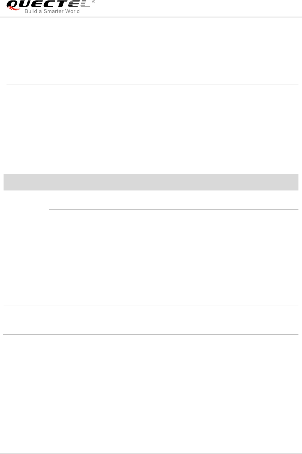
2.3. Functional Diagram
The following figure shows a block diagram of EG95 and illustrates the major functional parts.
Power management
Baseband
DDR+NAND flash
Radio frequency
Peripheral interfaces
NOTES
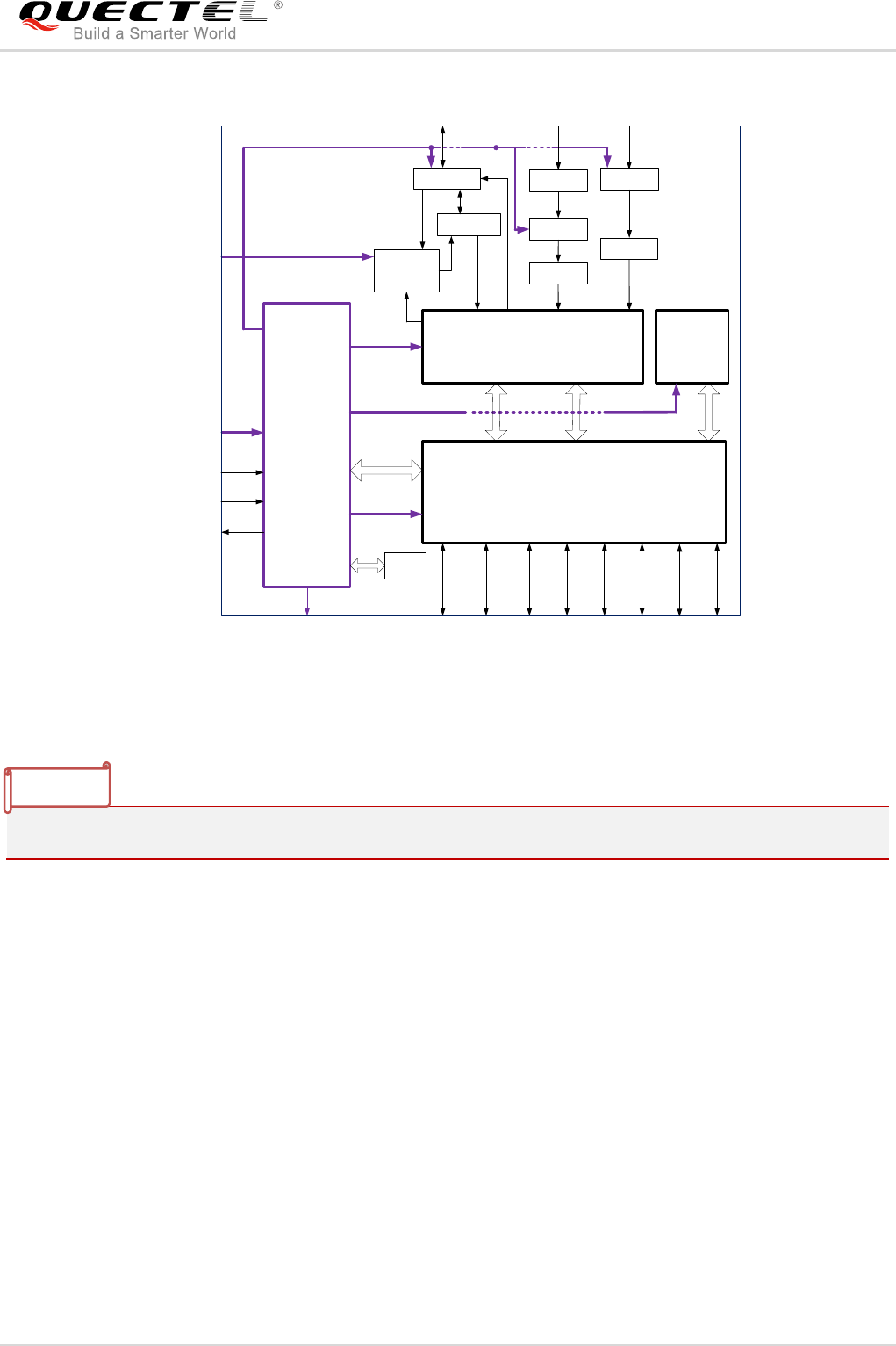
LTE Module Series
EG95 Hardware Design
EG95_Hardware_Design 15 / 81
Baseband
PMIC
Transceiver NAND
DDR2
SDRAM
PA
PAM Switch
ANT_MAIN ANT_DIV
VBAT_BB
VBAT_RF
PWRKEY
VDD_EXT USB PCM UARTI2C
RESET_N
19.2M
XO
STATUS
GPIOs
Control
IQ Control
Duplexer
SAW
Tx
PRx DRx
(U)SIM2 SPI
(U)SIM1
SAW
LNA
ANT_GNSS1)
SAW
GPS
Figure 1: Functional Diagram
1) GNSS antenna interface is only supported on EG95-NA.
2.4. Evaluation Board
In order to help customers develop applications conveniently with EG95, Quectel supplies an evaluation
board (EVB), USB data cable, earphone, antenna and other peripherals to control or test the module.
NOTE

LTE Module Series
EG95 Hardware Design
EG95_Hardware_Design 16 / 81
3 Application Interfaces
3.1. General Description
EG95 is equipped with 62-pin 1.1mm pitch SMT pads plus 44-pin ground/reserved pads that can be
connected to customers’ cellular application platforms. Sub-interfaces included in these pads are
described in detail in the following chapters:
Power supply
(U)SIM interfaces
USB interface
UART interfaces
PCM and I2C interfaces
SPI interface
Status indication
LTE Module Series
EG95 Hardware Design
EG95_Hardware_Design 17 / 81
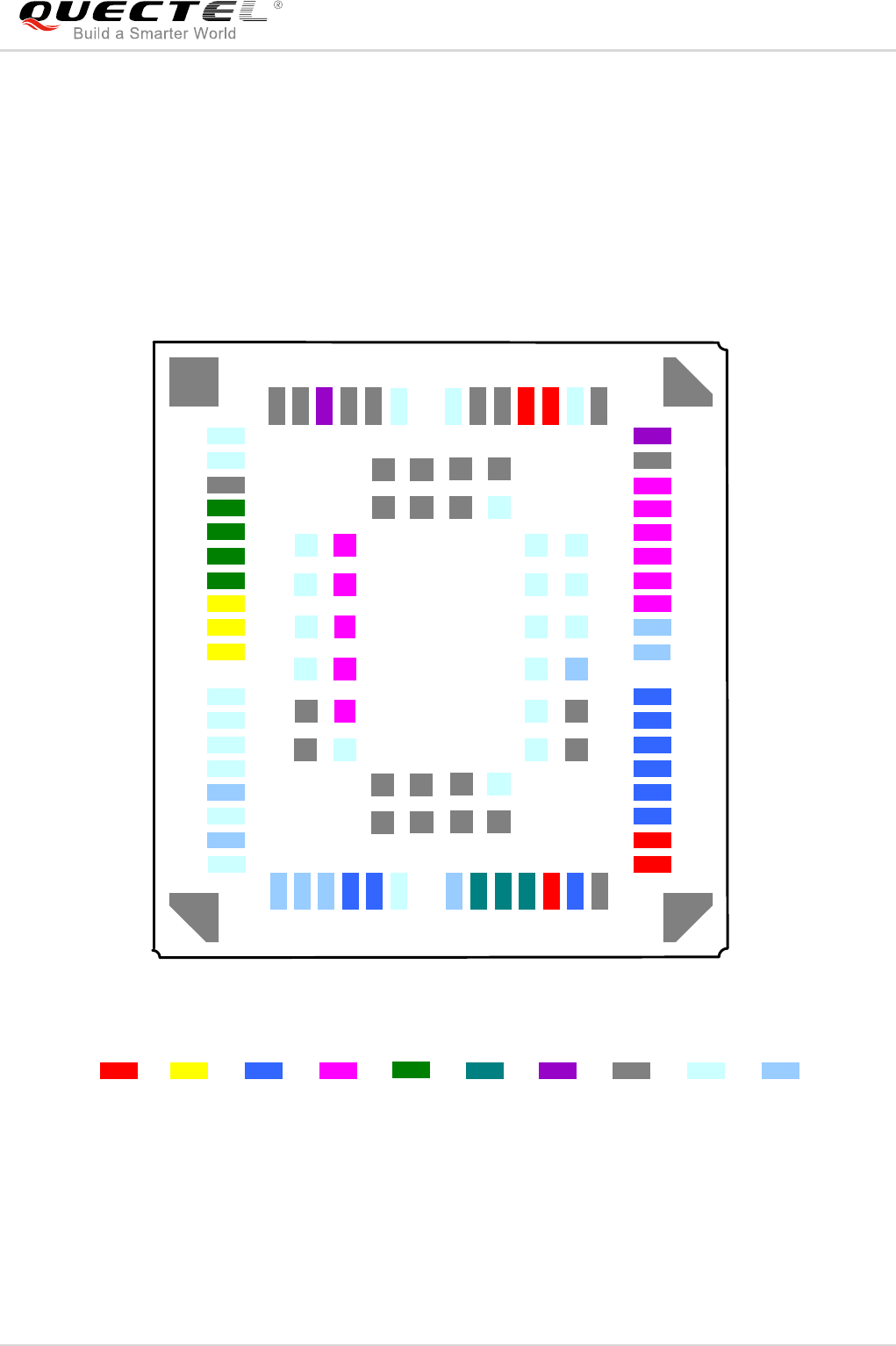
3.2. Pin Assignment
The following figure shows the pin assignment of EG95 module.
RESERVED
PCM_SYNC
PCM_CLK
PCM_DIN
PCM_DOUT
RESERVED
RESERVED
PWRKEY1)
RESERVED
RESET_N
RESERVED
1
2
3
4
5
6
7
11
12
13
14
15
16
17
18
50
51
52
53
54
55
58
59
60
61
62
USB_DM
AP_READY
STATUS
NETLIGHT
DBG_RXD
DBG_TXD
RESERVED
CLK_OUT
SPI_CLK
SPI_MOSI
SPI_MISO
VDD_EXT
DTR
GND
USIM1_CLK
USIM1_DATA
USIM1_RST
USIM1_VDD
RI
DCD
CTS
TXD
RXD
VBAT_BB
VBAT_BB
USIM_GND
GND
RESERVED (EG95-E)
31
30
29
28
27
26
23
22
21
20
19
10
9
USB_DP
USB_VBUS
RESERVED
GND
RESERVED
RESERVED
RTS
I2C_SCL
I2C_SDA
8
49
48
47
46
45
44
43
40
41
42
39
38
37
36
35
34
33
32
24
57
56
GND
GND
ANT_MAIN
GND
GND
RESERVED
VBAT_RF
VBAT_RF
GND
GND
ANT_DIV (EG95-E)
RESERVED
GND
USIM1_PRESENCE
63
64
65
66
67
68
83
84
85
86
87
88
98
97
96
95
94
93
78
77
76
75
74
73
91 92
89 90
71 72
69 70
80 79
82 81
100 99
102 101
POWER USB UART (U)SIM OTHERS
GND RESERVED
PCM ANT
25
USIM2_PRESENCE
USIM2_CLK
USIM2_RST
USIM2_DATA
USIM2_VDD
SPI
USB_BOOT
103
104 105
106
ANT_GNSS (EG95-NA)/
ANT_DIV (EG95-NA)/
Figure 2: Pin Assignment (Top View)
LTE Module Series
EG95 Hardware Design
EG95_Hardware_Design 18 / 81
1. 1) PWRKEY output voltage is 0.8V because of the diode drop in the Qualcomm chipset.
2. Keep all RESERVED pins and unused pins unconnected.
3. GND pads should be connected to ground in the design.
4. Please note that the definition of pin 49 and 56 are different between EG95-E and EG95-NA.
3.3. Pin Description
The following tables show the pin definition and description of EG95.
Table 3: IO Parameters Definition
Type
Description
IO
Bidirectional
DI
Digital input
DO
Digital output
PI
Power input
PO
Power output
AI
Analog input
AO
Analog output
OD
Open drain
Table 4: Pin Description
Power Supply
Pin Name
Pin No.
I/O
Description
DC Characteristics
Comment
VBAT_BB
32, 33
PI
Power supply for
module’s baseband
part
Vmax=4.3V
Vmin=3.3V
Vnorm=3.8V
It must be able to
provide sufficient
current up to 0.8A.
VBAT_RF
52, 53
PI
Power supply for
module’s RF part
Vmax=4.3V
Vmin=3.3V
Vnorm=3.8V
It must be able to
provide sufficient
current up to 1.8A in a
NOTES
LTE Module Series
EG95 Hardware Design
EG95_Hardware_Design 19 / 81
transmitting burst.
VDD_EXT
29
PO
Provide 1.8V for
external circuit
Vnorm=1.8V
IOmax=50mA
Power supply for
external GPIO’s pull up
circuits.
GND
3, 31, 48,
50, 54, 55,
58, 59, 61,
62, 67~74,
79~82,
89~91,
100~106
Ground
Turn on/off
Pin Name
Pin No.
I/O
Description
DC Characteristics
Comment
PWRKEY
15
DI
Turn on/off the
module
VIHmax=2.1V
VIHmin=1.3V
VILmax=0.5V
The output voltage is
0.8V because of the
diode drop in the
Qualcomm chipset.
RESET_N
17
DI
Reset signal of the
module
VIHmax=2.1V
VIHmin=1.3V
VILmax=0.5V
Status Indication
Pin Name
Pin No.
I/O
Description
DC Characteristics
Comment
STATUS
20
DO
Indicate the
module’s operation
status
VOin=1.35V
VOLmax=0.45V
1.8V power domain.
If unused, keep this
pin open.
NETLIGHT
21
DO
Indicate the
module’d network
activity status
VOin=1.35V
VOLmax=0.45V
1.8V power domain.
If unused, keep it
open.
USB Interface
Pin Name
Pin No.
I/O
Description
DC Characteristics
Comment
USB_VBUS
8
PI
USB detection
Vnorm=5.0V
USB_DP
9
IO
USB differential data
bus (+)
Compliant with USB
2.0 standard
specification.
Require differential
impedance of 90Ω.
USB_DM
10
IO
USB differential data
bus (-)
Compliant with USB
2.0 standard
specification.
Require differential
impedance of 90Ω.

LTE Module Series
EG95 Hardware Design
EG95_Hardware_Design 20 / 81
(U)SIM Interfaces
Pin Name
Pin No.
I/O
Description
DC Characteristics
Comment
USIM_GND
47
Specified ground for
(U)SIM card
USIM1_VDD
43
PO
Power supply for
(U)SIM card
For 1.8V (U)SIM:
Vmax=1.9V
Vmin=1.7V
For 3.0V (U)SIM:
Vmax=3.05V
Vmin=2.7V
IOmax=50mA
Either 1.8V or 3.0V is
supported by the
module automatically.
USIM2_VDD
87
USIM1_DATA
45
IO
Data signal of
(U)SIM card
For 1.8V (U)SIM:
VILmax=0.6V
VIHmin=1.2V
VOLmax=0.45V
VOin=1.35V
For 3.0V (U)SIM:
VILmax=1.0V
VIHmin=1.95V
VOLmax=0.45V
VOin=2.55V
USIM2_DATA
86
USIM1_CLK
46
DO
Clock signal of
(U)SIM card
For 1.8V (U)SIM:
VOLmax=0.45V
VOin=1.35V
For 3.0V (U)SIM:
VOLmax=0.45V
VOin=2.55V
USIM2_CLK
84
USIM1_RST
44
DO
Reset signal of
(U)SIM card
For 1.8V (U)SIM:
VOLmax=0.45V
VOin=1.35V
For 3.0V (U)SIM:
VOLmax=0.45V
VOin=2.55V
USIM2_RST
85
USIM1_
PRESENCE
42
DI
(U)SIM card
insertion detection
VILmin=-0.3V
VILmax=0.6V
VIHmin=1.2V
VIHmax=2.0V
1.8V power domain.
If unused, keep it
open.
USIM2_
PRESENCE
83
LTE Module Series
EG95 Hardware Design
EG95_Hardware_Design 21 / 81
Main UART Interface
Pin Name
Pin No.
I/O
Description
DC Characteristics
Comment
RI
39
DO
Ring indicator
VOLmax=0.45V
VOin=1.35V
1.8V power domain.
If unused, keep it
open.
DCD
38
DO
Data carrier
detection
VOLmax=0.45V
VOin=1.35V
1.8V power domain.
If unused, keep it
open.
CTS
36
DO
Clear to send
VOLmax=0.45V
VOin=1.35V
1.8V power domain.
If unused, keep it
open.
RTS
37
DI
Request to send
VILmin=-0.3V
VILmax=0.6V
VIHmin=1.2V
VIHmax=2.0V
1.8V power domain.
If unused, keep it
open.
DTR
30
DI
Data terminal ready.
Sleep mode control.
VILmin=-0.3V
VILmax=0.6V
VIHmin=1.2V
VIHmax=2.0V
1.8V power domain.
Pull-up by default.
Low level wakes up
the module.
If unused, keep it
open.
TXD
35
DO
Transmit data
VOLmax=0.45V
VOin=1.35V
1.8V power domain.
If unused, keep it
open.
RXD
34
DI
Receive data
VILmin=-0.3V
VILmax=0.6V
VIHmin=1.2V
VIHmax=2.0V
1.8V power domain.
If unused, keep it
open.
Debug UART Interface
Pin Name
Pin No.
I/O
Description
DC Characteristics
Comment
DBG_TXD
23
DO
Transmit data
VOLmax=0.45V
VOin=1.35V
1.8V power domain.
If unused, keep it
open.
DBG_RXD
22
DI
Receive data
VILmin=-0.3V
VILmax=0.6V
VIHmin=1.2V
VIHmax=2.0V
1.8V power domain.
If unused, keep it
open.
PCM Interface
Pin Name
Pin No.
I/O
Description
DC Characteristics
Comment

LTE Module Series
EG95 Hardware Design
EG95_Hardware_Design 22 / 81
PCM_DIN
6
DI
PCM data input
VILmin=-0.3V
VILmax=0.6V
VIHmin=1.2V
VIHmax=2.0V
1.8V power domain.
If unused, keep it
open.
PCM_DOUT
7
DO
PCM data output
VOLmax=0.45V
VOin=1.35V
1.8V power domain.
If unused, keep it
open.
PCM_SYNC
5
IO
PCM data frame
synchronization
signal
VOLmax=0.45V
VOin=1.35V
VILmin=-0.3V
VILmax=0.6V
VIHmin=1.2V
VIHmax=2.0V
1.8V power domain.
In master mode, it is
an output signal. In
slave mode, it is an
input signal.
If unused, keep it
open.
PCM_CLK
4
IO
PCM clock
VOLmax=0.45V
VOin=1.35V
VILmin=-0.3V
VILmax=0.6V
VIHmin=1.2V
VIHmax=2.0V
1.8V power domain.
In master mode, it is
an output signal. In
slave mode, it is an
input signal.
If unused, keep it
open.
I2C Interface
Pin Name
Pin No.
I/O
Description
DC Characteristics
Comment
I2C_SCL
40
OD
I2C serial clock.
Used for external
codec
An external pull-up
resistor is required.
1.8V only.
If unused, keep it
open.
I2C_SDA
41
OD
I2C serial data. Used
for external codec
An external pull-up
resistor is required.
1.8V only.
If unused, keep it
open.
SPI Interface
Pin Name
Pin No.
I/O
Description
DC Characteristics
Comment
SPI_CLK
26
DO
Clock signal of SPI
interface
VOLmax=0.45V
VOin=1.35V
1.8V power domain.
If unused, keep it
open.
SPI_MOSI
27
DO
Master output slave
input of SPI interface
VOLmax=0.45V
VOin=1.35V
1.8V power domain.
If unused, keep it
LTE Module Series
EG95 Hardware Design
EG95_Hardware_Design 23 / 81
open.
SPI_MISO
28
DI
Master input slave
output of SPI
interface
VILmin=-0.3V
VILmax=0.6V
VIHmin=1.2V
VIHmax=2.0V
1.8V power domain.
If unused, keep it
open.
RF Interface
Pin Name
Pin No.
I/O
Description
DC Characteristics
Comment
ANT_GNSS
49
(EG95-
NA)
AI
GNSS antenna pad
50Ω impedance.
If unused, keep it
open.
Pin 49 is defined as
ANT_DIV on EG95-E.
ANT_DIV
49
(EG95-E)
AI
Receive diversity
antenna pad
50Ω impedance.
If unused, keep it
open.
ANT_DIV
56
(EG95-
NA)
AI
Receive diversity
antenna pad
50Ω impedance.
If unused, keep it
open.
Pin 56 is reserved on
EG95-E.
ANT_MAIN
60
IO
Main antenna pad
Other Pins
Pin Name
Pin No.
I/O
Description
DC Characteristics
Comment
CLK_OUT
25
DI
Clock output
Provide a digital clock
output for an external
audio codec.
If unused, keep this
pin open.
AP_READY
19
DI
Application
processor sleep
state detection
VILmin=-0.3V
VILmax=0.6V
VIHmin=1.2V
VIHmax=2.0V
1.8V power domain.
If unused, keep it
open.
USB_BOOT
75
DI
Force the module to
enter into
emergency
download mode
VILmin=-0.3V
VILmax=0.6V
VIHmin=1.2V
VIHmax=2.0V
1.8V power domain.
If unused, keep it
open.
RESERVED Pins
Pin Name
Pin No.
I/O
Description
DC Characteristics
Comment
LTE Module Series
EG95 Hardware Design
EG95_Hardware_Design 24 / 81
3.4. Operating Modes
The table below briefly summarizes the various operating modes referred in the following chapters.
Table 5: Overview of Operating Modes
Mode
Details
Normal
Operation
Idle
Software is active. The module has registered on network, and it is
ready to send and receive data.
Talk/Data
Network connection is ongoing. In this mode, the power consumption is
decided by network setting and data transfer rate.
Minimum
Functionality
Mode
AT+CFUN command can set the module to a minimum functionality mode without
removing the power supply. In this case, both RF function and (U)SIM card will be invalid.
Airplane
Mode
AT+CFUN command or W_DISABLE# pin can set the module to airplane mode. In this
case, RF function will be invalid.
Sleep Mode
In this mode, the current consumption of the module will be reduced to the minimal level.
During this mode, the module can still receive paging message, SMS, voice call and
TCP/UDP data from the network normally.
Power Down
Mode
In this mode, the power management unit shuts down the power supply. Software is not
active. The serial interface is not accessible. Operating voltage (connected to VBAT_RF
and VBAT_BB) remains applied.
3.5. Power Saving
3.5.1. Sleep Mode
EG95 is able to reduce its current consumption to a minimum value during the sleep mode. The following
sections describe the power saving procedures of EG95 module.
RESERVED
1, 2,
11~14, 16,
18, 49, 51,
57, 63~66,
76~78,
88, 92~99
Reserved
Keep these pins
unconnected.
LTE Module Series
EG95 Hardware Design
EG95_Hardware_Design 25 / 81
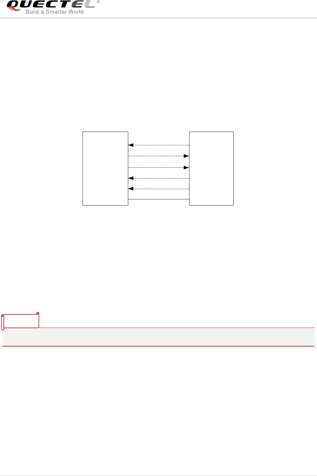
3.5.1.1. UART Application
If the host communicates with the module via UART interface, the following preconditions can let the
module enter into sleep mode.
Execute AT+QSCLK=1 command to enable sleep mode.
Drive DTR to high level.
The following figure shows the connection between the module and the host.
RXD
TXD
RI
DTR
AP_READY
TXD
RXD
EINT
GPIO
GPIO
Module Host
GND GND
Figure 3: Sleep Mode Application via UART
Driving the host DTR to low level will wake up the module.
When EG95 has a URC to report, RI signal will wake up the host. Refer to Chapter 3.16 for details
about RI behavior.
AP_READY will detect the sleep state of host (can be configured to high level or low level detection).
Please refer to AT+QCFG="apready"* command for details.
“*” means under development.
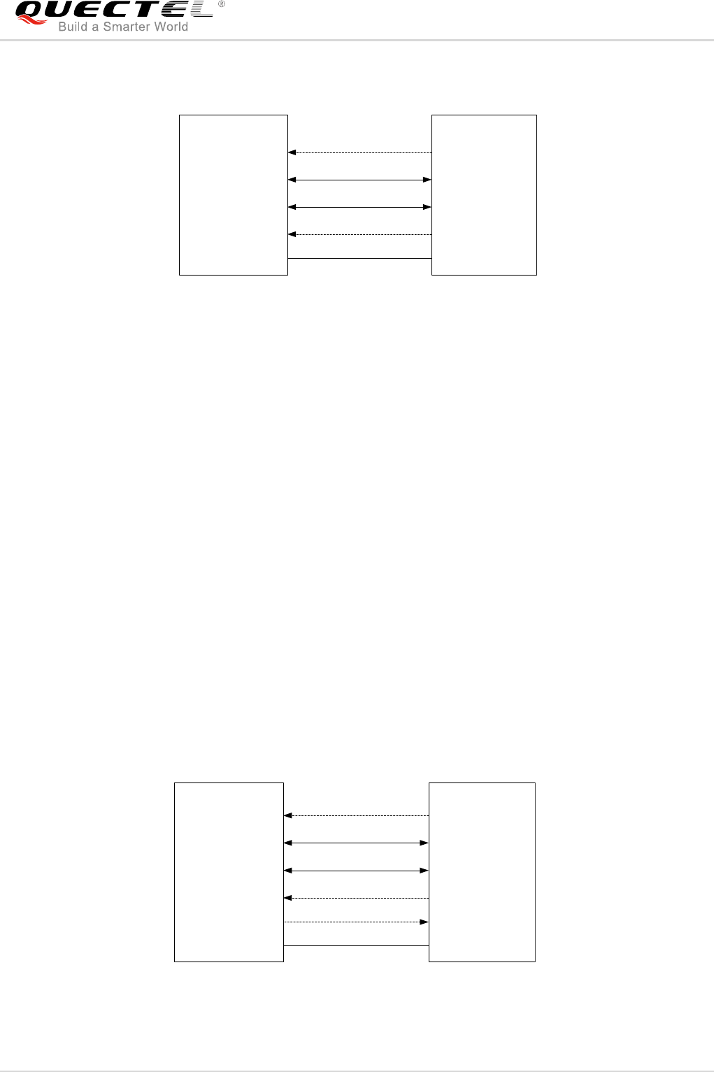
3.5.1.2. USB Application with USB Remote Wakeup Function
If the host supports USB suspend/resume and remote wakeup functions, the following three preconditions
must be met to let the module enter into sleep mode.
Execute AT+QSCLK=1 command to enable the sleep mode.
Ensure the DTR is held at high level or keep it open.
The host’s USB bus, which is connected with the module’s USB interface, enters into suspended
state.
NOTE
LTE Module Series
EG95 Hardware Design
EG95_Hardware_Design 26 / 81
The following figure shows the connection between the module and the host.
USB_VBUS
USB_DP
USB_DM
AP_READY
VDD
USB_DP
USB_DM
GPIO
Module Host
GND GND
Figure 4: Sleep Mode Application with USB Remote Wakeup
Sending data to EG95 through USB will wake up the module.
When EG95 has a URC to report, the module will send remote wake-up signals via USB bus so as to
wake up the host.
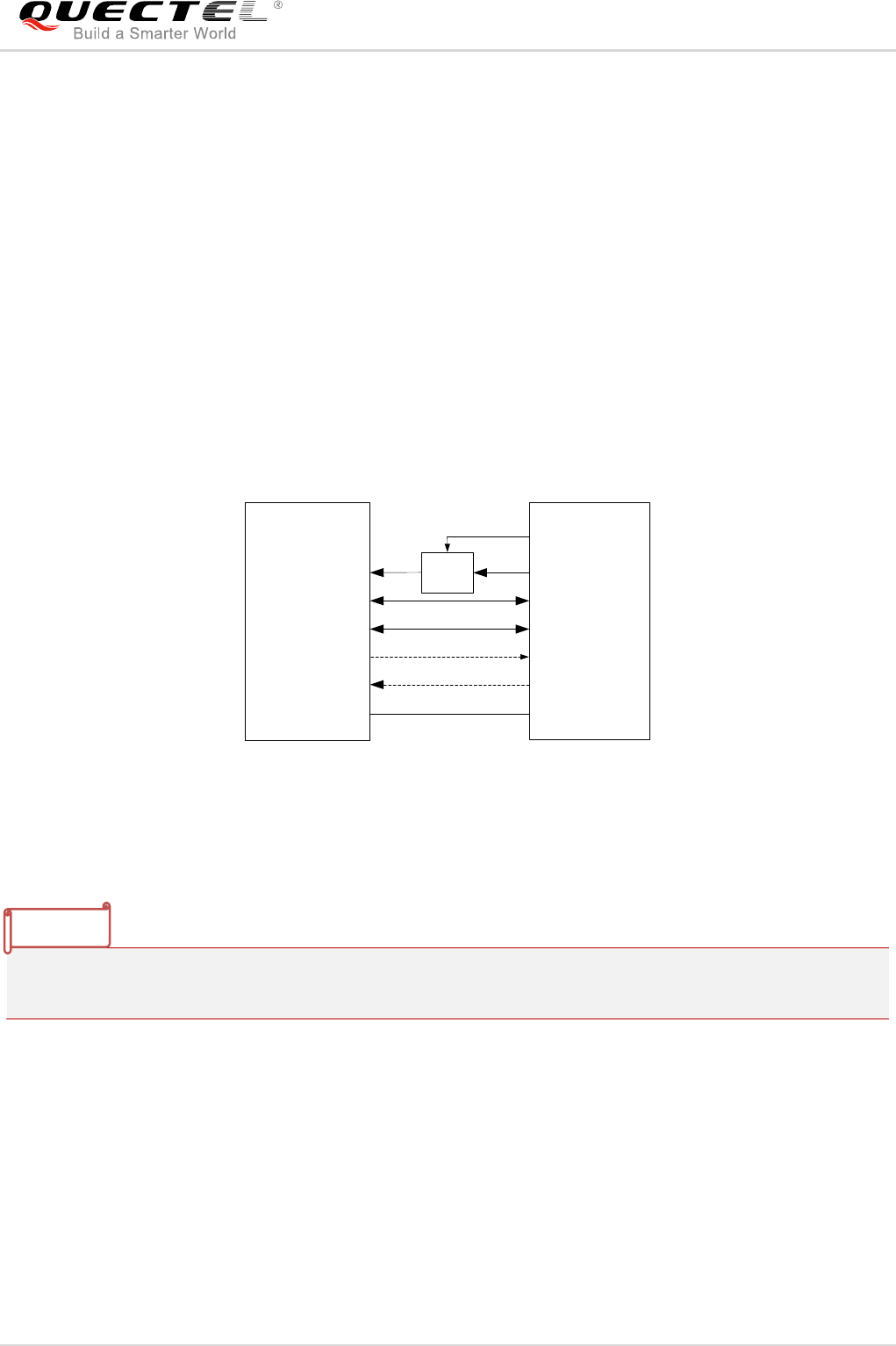
3.5.1.3. USB Application with USB Suspend/Resume and RI Function
If the host supports USB suspend/resume, but does not support remote wake-up function, the RI signal is
needed to wake up the host.
There are three preconditions to let the module enter into the sleep mode.
Execute AT+QSCLK=1 command to enable sleep mode.
Ensure the DTR is held at high level or keep it open.
The host’s USB bus, which is connected with the module’s USB interface, enters into suspended
state.
The following figure shows the connection between the module and the host.
USB_VBUS
USB_DP
USB_DM
AP_READY
VDD
USB_DP
USB_DM
GPIO
Module Host
GND GND
RI EINT
Figure 5: Sleep Mode Application with RI
LTE Module Series
EG95 Hardware Design
EG95_Hardware_Design 27 / 81
Sending data to EG95 through USB will wake up the module.
When EG95 has a URC to report, RI signal will wake up the host.
3.5.1.4. USB Application without USB Suspend Function
If the host does not support USB suspend function, USB_VBUS should be disconnected with an external
control circuit to let the module enter into sleep mode.
Execute AT+QSCLK=1 command to enable the sleep mode.
Ensure the DTR is held at high level or keep it open.
Disconnect USB_VBUS.
The following figure shows the connection between the module and the host.
USB_VBUS
USB_DP
USB_DM
AP_READY
VDD
USB_DP
USB_DM
GPIO
Module Host
RI EINT
Power
Switch
GPIO
GND GND
Figure 6: Sleep Mode Application without Suspend Function
Switching on the power switch to supply power to USB_VBUS will wake up the module.
Please pay attention to the level match shown in dotted line between the module and the host. Refer to
document [1] for more details about EG95 power management application.
3.5.2. Airplane Mode
When the module enters into airplane mode, the RF function does not work, and all AT commands
correlative with RF function will be inaccessible. This mode can be set via the following ways.
Hardware:
The W_DISABLE# pin is pulled up by default. Driving it to low level will let the module enter into airplane
mode.
NOTE
LTE Module Series
EG95 Hardware Design
EG95_Hardware_Design 28 / 81
Software:
AT+CFUN command provides the choice of functionality levels as shown below:
AT+CFUN=0: Minimum functionality mode. Both (U)SIM and RF functions are disabled.
AT+CFUN=1: Full functionality mode (by default).
AT+CFUN=4: Airplane mode. RF function is disabled.
1. Airplane mode control via W_DISABLE# is disabled in firmware by default. It can be enabled by
AT+QCFG="airplanecontrol" command and this command is under development.
2. The execution of AT+CFUN command will not affect GNSS function.
3.6. Power Supply
3.6.1. Power Supply Pins
EG95 provides four VBAT pins for connection with an external power supply. There are two separate
voltage domains for VBAT.
Two VBAT_RF pins for module’s RF part.
Two VBAT_BB pins for module’s baseband part.
The following table shows the details of VBAT pins and ground pins.
Table 6: VBAT and GND Pins
Pin Name
Pin No.
Description
Min.
Typ.
Max.
Unit
VBAT_RF
52, 53
Power supply for module’s
RF part.
3.3
3.8
4.3
V
VBAT_BB
32, 33
Power supply for module’s
baseband part.
3.3
3.8
4.3
V
GND
3, 31, 48, 50,
54, 55, 58, 59,
61, 62, 67~74,
79~82, 89~91,
100~106
Ground
-
0
-
V
NOTES
LTE Module Series
EG95 Hardware Design
EG95_Hardware_Design 29 / 81
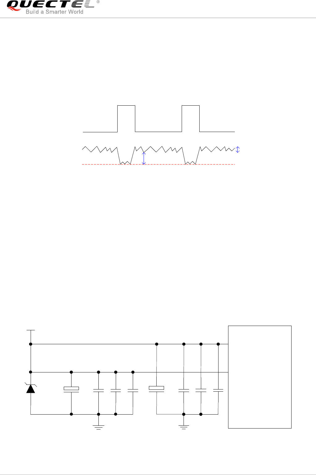
3.6.2. Decrease Voltage Drop
The power supply range of the module is from 3.3V to 4.3V. Please make sure that the input voltage will
never drop below 3.3V. The following figure shows the voltage drop during burst transmission in 2G
network. The voltage drop will be less in 3G and 4G networks.
VBAT
Min.3.3V
Ripple
Drop
Burst
Transmission
Burst
Transmission
Figure 7: Power Supply Limits during Burst Transmission
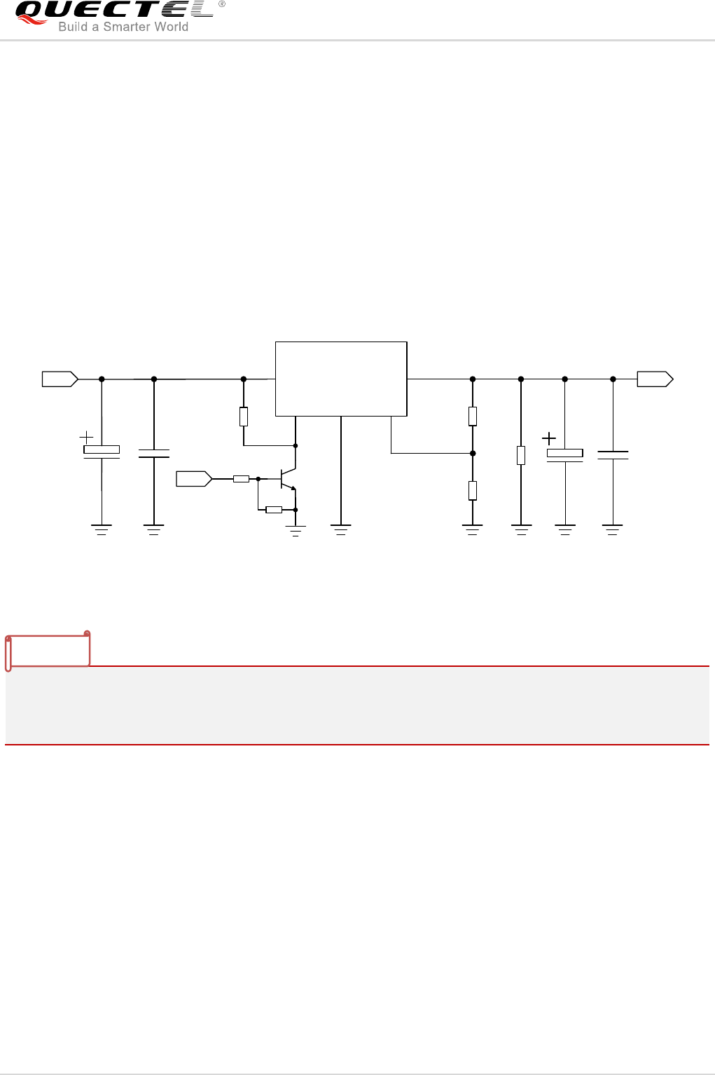
To decrease voltage drop, a bypass capacitor of about 100µF with low ESR (ESR=0.7Ω) should be used,
and a multi-layer ceramic chip (MLCC) capacitor array should also be reserved due to its ultra-low ESR. It
is recommended to use three ceramic capacitors (100nF, 33pF, 10pF) for composing the MLCC array,
and place these capacitors close to VBAT_BB/VBAT_RF pins. The main power supply from an external
application has to be a single voltage source and can be expanded to two sub paths with star structure.
The width of VBAT_BB trace should be no less than 1mm, and the width of VBAT_RF trace should be no
less than 2mm. In principle, the longer the VBAT trace is, the wider it will be.
In addition, in order to get a stable power source, it is suggested that a zener diode whose dissipation
power is more than 0.5W should be used. The following figure shows the star structure of the power
supply.
Module
VBAT_RF
VBAT_BB
VBAT
C1
100uF
C6
100nF
C7
33pF
C8
10pF
+
+
C2
100nF
C5
100uF
C3
33pF
C4
10pF
D1
Figure 8: Star Structure of the Power Supply
LTE Module Series
EG95 Hardware Design
EG95_Hardware_Design 30 / 81
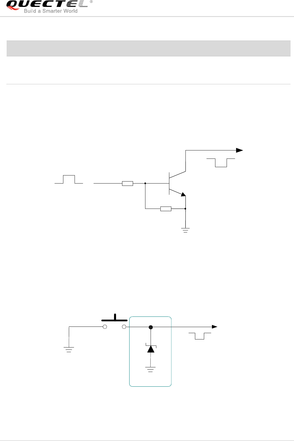
3.6.3. Reference Design for Power Supply
Power design for the module is very important, as the performance of the module largely depends on the
power source. The power supply should be able to provide sufficient current up to 2A at least. If the
voltage drop between the input and output is not too high, it is suggested that an LDO should be used to
supply power for the module. If there is a big voltage difference between the input source and the desired
output (VBAT), a buck converter is preferred to be used as the power supply.
The following figure shows a reference design for +5V input power source. The typical output of the power
supply is about 3.8V and the maximum load current is 3A.
DC_IN
MIC29302WU
IN OUT
EN
GND
ADJ
2 4
1
3
5
VBAT
100nF 470uF 100nF
100K
47K
470uF
470R
51K 1%
1%
4.7K
47K
VBAT_EN
Figure 9: Reference Circuit of Power Supply
In order to avoid damaging internal flash, please do not switch off the power supply when the module
works normally. Only after the module is shut down by PWRKEY or AT command, the power supply can
be cut off.
3.6.4. Monitor the Power Supply
AT+CBC command can be used to monitor the VBAT_BB voltage value. For more details, please refer to
document [2].
3.7. Turn on and off Scenarios
3.7.1. Turn on Module Using the PWRKEY
The following table shows the pin definition of PWRKEY.
NOTE
LTE Module Series
EG95 Hardware Design
EG95_Hardware_Design 31 / 81
Table 7: Pin Definition of PWRKEY
Pin Name
Pin No.
Description
DC Characteristics
Comment
PWRKEY
15
Turn on/off the module
VIHmax=2.1V
VIHmin=1.3V
VILmax=0.5V
The output voltage is 0.8V
because of the diode drop in
the Qualcomm chipset.
When EG95 is in power down mode, it can be turned on to normal mode by driving the PWRKEY pin to a
low level for at least 500ms. It is recommended to use an open drain/collector driver to control the
PWRKEY. After STATUS pin outputting a high level, PWRKEY pin can be released. A simple reference
circuit is illustrated in the following figure.
Turn on pulse
PWRKEY
4.7K
47K
≥ 500ms
Figure 10: Turn on the Module Using Driving Circuit
Another way to control the PWRKEY is using a button directly. When pressing the key, electrostatic strike
may generate from the finger. Therefore, a TVS component is indispensable to be placed nearby the
button for ESD protection. A reference circuit is shown in the following figure.
PWRKEY
S1
Close to S1
TVS
Figure 11: Turn on the Module Using Button
LTE Module Series
EG95 Hardware Design
EG95_Hardware_Design 32 / 81
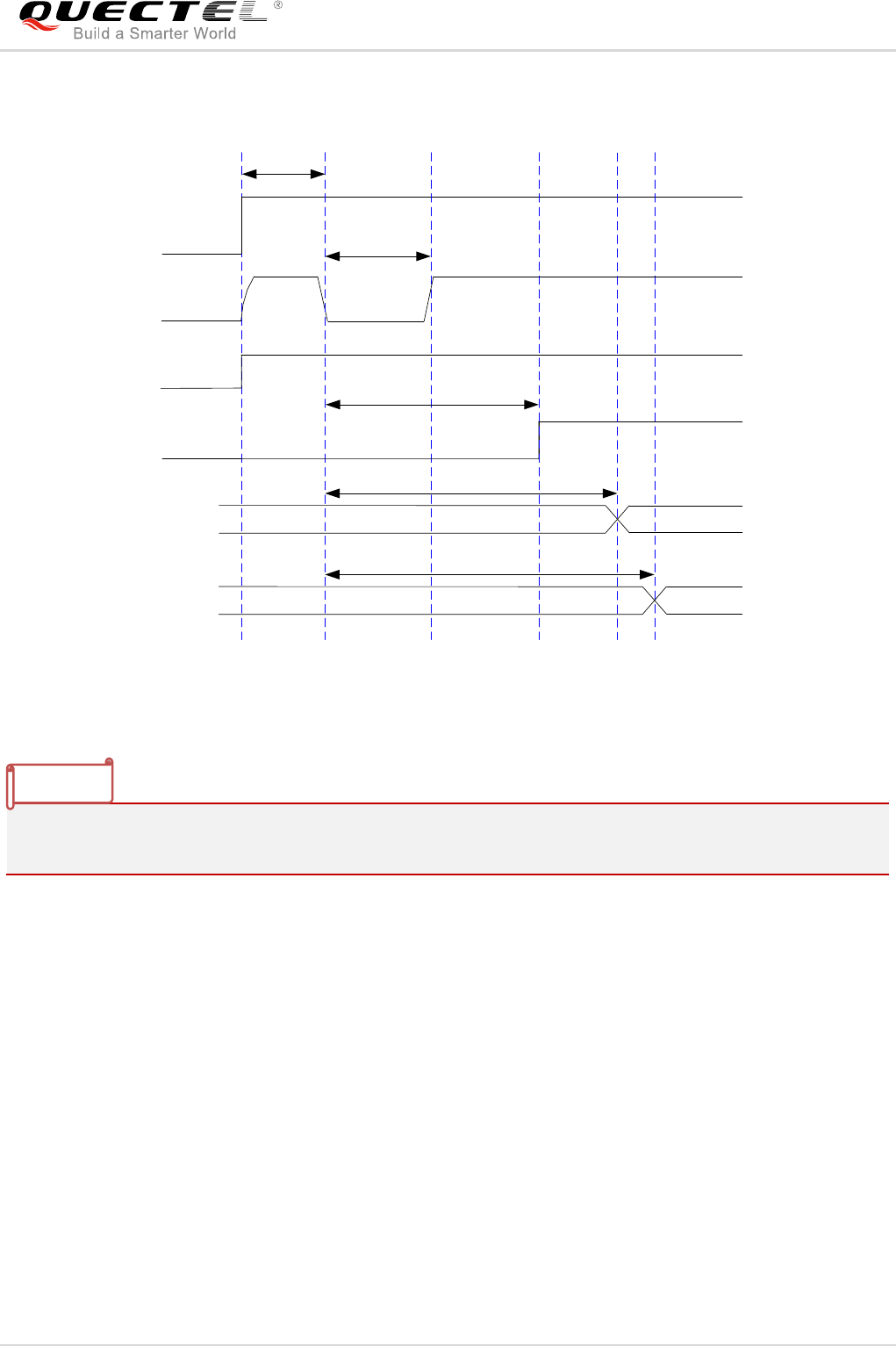
The turn on scenario is illustrated in the following figure.
VIL ≤ 0.5V
VIH ≥ 1.3V
VBAT
PWRKEY
≥ 500ms
RESET_N
STATUS
Inactive ActiveUART
NOTE
Inactive ActiveUSB
≥ 10s
≥ 12s
≥ 13s
Figure 12: Timing of Turning on Module
Please make sure that VBAT is stable before pulling down PWRKEY pin. The time between them is no
less than 30ms.
3.7.2. Turn off Module
Either of the following methods can be used to turn off the module:
Normal power down procedure: Turn off the module using the PWRKEY pin.
Normal power down procedure: Turn off the module using AT+QPOWD command.
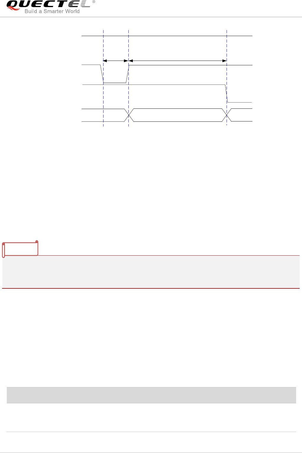
3.7.2.1. Turn off Module Using the PWRKEY Pin
Driving the PWRKEY pin to a low level voltage for at least 650ms, the module will execute power-down
procedure after the PWRKEY is released. The power-down scenario is illustrated in the following figure.
NOTE
LTE Module Series
EG95 Hardware Design
EG95_Hardware_Design 33 / 81
VBAT
PWRKEY
≥ 30s
≥ 650ms
RUNNING Power-down procedure OFF
Module
Status
STATUS
Figure 13: Timing of Turning off Module
3.7.2.2. Turn off Module Using AT Command
It is also a safe way to use AT+QPOWD command to turn off the module, which is similar to turning off the
module via PWRKEY pin.
Please refer to document [2] for details about the AT+QPOWD command.
In order to avoid damaging internal flash, please do not switch off the power supply when the module
works normally. Only after the module is shut down by PWRKEY or AT command, the power supply can
be cut off.
3.8. Reset the Module
The RESET_N pin can be used to reset the module. The module can be reset by driving RESET_N to a
low level voltage for 150ms ~ 460ms.
Table 8: Pin Definition of RESET_N
Pin Name
Pin No.
Description
DC Characteristics
Comment
RESET_N
17
Reset the module
VIHmax=2.1V
VIHmin=1.3V
VILmax=0.5V
NOTE
LTE Module Series
EG95 Hardware Design
EG95_Hardware_Design 34 / 81
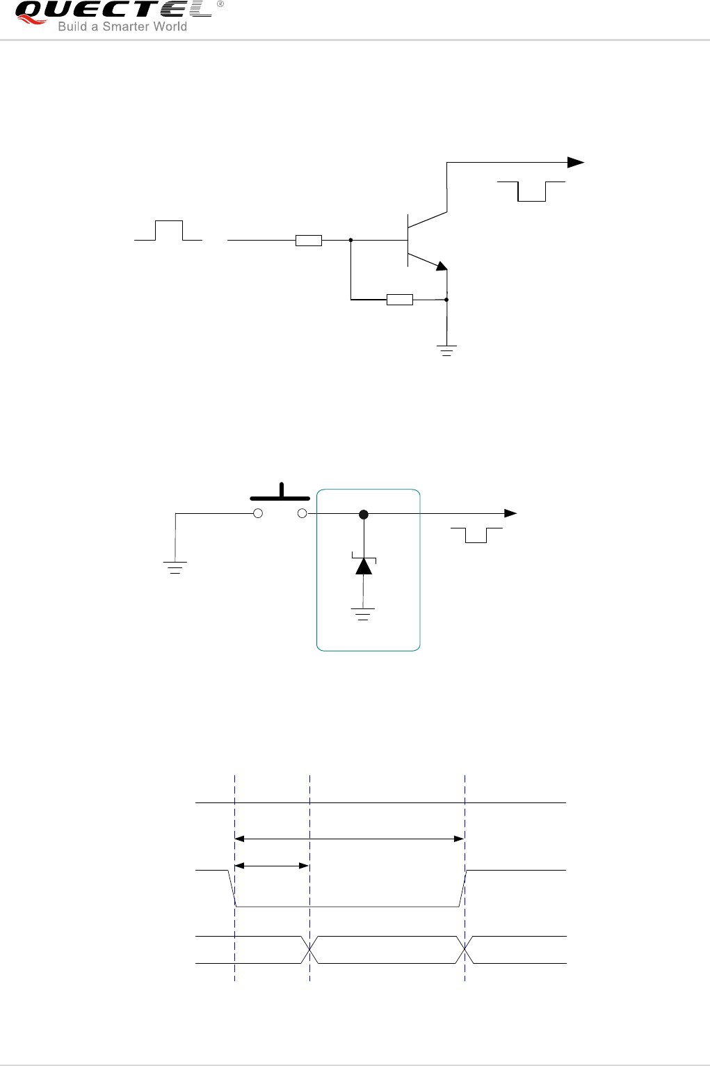
The recommended circuit is similar to the PWRKEY control circuit. An open drain/collector driver or button
can be used to control the RESET_N.
Reset pulse
RESET_N
4.7K
47K
150ms~460ms
Figure 14: Reference Circuit of RESET_N by Using Driving Circuit
RESET_N
S2
Close to S2
TVS
Figure 15: Reference Circuit of RESET_N by Using Button
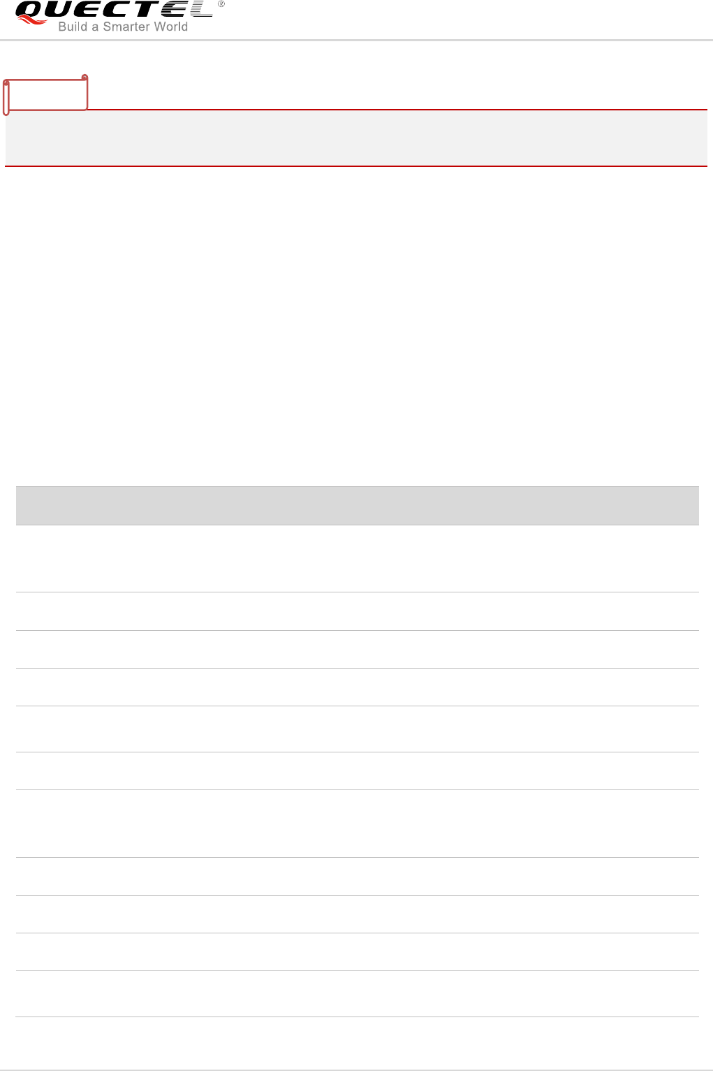
The reset scenario is illustrated in the following figure.
VIL ≤ 0.5V
VIH ≥ 1.3V
VBAT
≥ 150ms
Resetting
Module
Status Running
RESET_N
Restart
≤ 460ms
Figure 16: Timing of Resetting Module
LTE Module Series
EG95 Hardware Design
EG95_Hardware_Design 35 / 81
1. Use RESET_N only when turning off the module by AT+QPOWD command and PWRKEY pin failed.
2. Ensure that there is no large capacitance on PWRKEY and RESET_N pins.
3.9. (U)SIM Interfaces
EG95 provides two (U)SIM interfaces, and only one (U)SIM card can work at a time. The (U)SIM 1 and
(U)SIM 2 cards can be switched by AT+QDSIM command. For more details, please refer to document
[2].
The (U)SIM interfaces circuitry meet ETSI and IMT-2000 requirements. Both 1.8V and 3.0V (U)SIM cards
are supported.
Table 9: Pin Definition of (U)SIM Interfaces
Pin Name
Pin No.
I/O
Description
Comment
USIM1_VDD
43
PO
Power supply for (U)SIM1 card
Either 1.8V or 3.0V is
supported by the module
automatically.
USIM1_DATA
45
IO
Data signal of (U)SIM1 card
USIM1_CLK
46
DO
Clock signal of (U)SIM1 card
USIM1_RST
44
DO
Reset signal of (U)SIM1 card
USIM1_
PRESENCE
42
DI
(U)SIM1 card insertion detection
USIM_GND
47
Specified ground for (U)SIM card
USIM2_VDD
87
PO
Power supply for (U)SIM2 card
Either 1.8V or 3.0V is
supported by the module
automatically.
USIM2_DATA
86
IO
Data signal of (U)SIM2 card
USIM2_CLK
84
DO
Clock signal of (U)SIM2 card
USIM2_RST
85
DO
Reset signal of (U)SIM2 card
USIM2_
PRESENCE
83
DI
(U)SIM2 card insertion detection
NOTES
LTE Module Series
EG95 Hardware Design
EG95_Hardware_Design 36 / 81
EG95 supports (U)SIM card hot-plug via the USIM1_PRESENCE and USIM2_PRESENCE pins. The
function supports low level and high level detections, and is disabled by default. Please refer to
document [2] about AT+QSIMDET command for details.
The following figure shows a reference design for (U)SIM1 interface with an 8-pin (U)SIM card connector.
Module
USIM1_VDD
USIM_GND
USIM1_RST
USIM1_CLK
USIM1_DATA
USIM1_PRESENCE
0R
0R
0R
VDD_EXT
51K
100nF (U)SIM Card Connector
GND
GND
33pF 33pF 33pF
VCC
RST
CLK IO
VPP
GND
GND
USIM1_VDD
15K
Figure 17: Reference Circuit of (U)SIM1 Interface with an 8-Pin (U)SIM Card Connector
If (U)SIM1 card detection function is not needed, please keep USIM1_PRESENCE unconnected. A
reference circuit of (U)SIM1 interface with a 6-pin (U)SIM card connector is illustrated in the following
figure.
Module
USIM1_VDD
USIM_GND
USIM1_RST
USIM1_CLK
USIM1_DATA 0R
0R
0R
100nF (U)SIM Card Connector
GND
33pF 33pF 33pF
VCC
RST
CLK IO
VPP
GND
GND
15K
USIM1_VDD
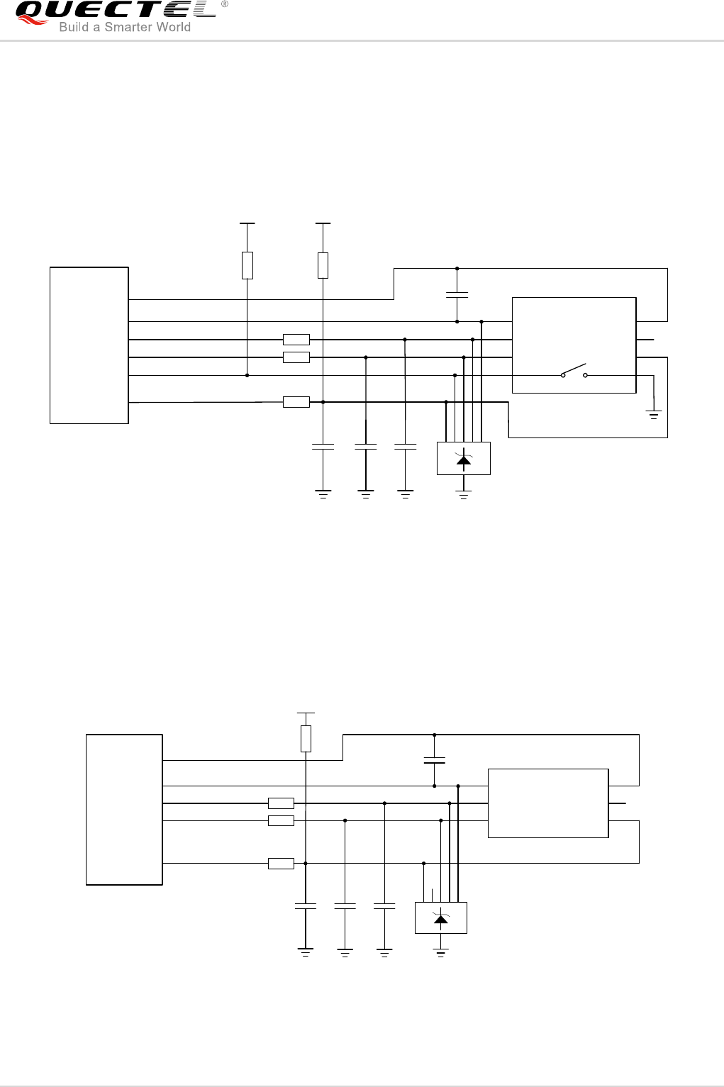
Figure 18: Reference Circuit of (U)SIM1 Interface with a 6-Pin (U)SIM Card Connector
LTE Module Series
EG95 Hardware Design
EG95_Hardware_Design 37 / 81
The following figure shows a reference design of (U)SIM2 interface with an 8-pin (U)SIM card connector.
Module
USIM2_VDD
USIM_GND
USIM2_RST
USIM2_CLK
USIM2_DATA
USIM2_PRESENCE
0R
0R
0R
VDD_EXT
51K
100nF (U)SIM Card Connector
GND
GND
33pF 33pF 33pF
VCC
RST
CLK IO
VPP
GND
GND
USIM2_VDD
15K
Figure 19: Reference Circuit of (U)SIM2 Interface with an 8-Pin (U)SIM Card Connector
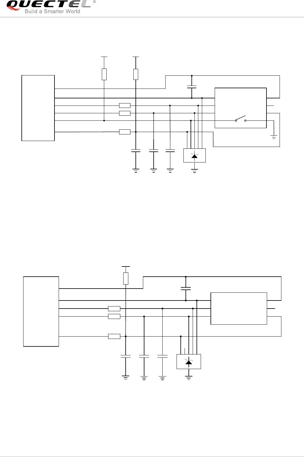
If (U)SIM2 card detection function is not needed, please keep USIM2_PRESENCE unconnected. A
reference circuit of (U)SIM2 interface with a 6-pin (U)SIM card connector is illustrated in the following
figure.
Module
USIM2_VDD
USIM_GND
USIM2_RST
USIM2_CLK
USIM2_DATA 0R
0R
0R
100nF (U)SIM Card Connector
GND
33pF 33pF 33pF
VCC
RST
CLK IO
VPP
GND
GND
15K
USIM2_VDD
Figure 20: Reference Circuit of (U)SIM2 Interface with a 6-Pin (U)SIM Card Connector

LTE Module Series
EG95 Hardware Design
EG95_Hardware_Design 38 / 81
In order to enhance the reliability and availability of the (U)SIM cards in customers’ applications, please
follow the criteria below in the (U)SIM circuit design:
Keep placement of (U)SIM card connector to the module as close as possible. Keep the trace length
as less than 200mm as possible.
Keep (U)SIM card signals away from RF and VBAT traces.
Assure the ground between the module and the (U)SIM card connector short and wide. Keep the
trace width of ground and USIM_VDD no less than 0.5mm to maintain the same electric potential.
To avoid cross-talk between USIM_DATA and USIM_CLK, keep them away from each other and
shield them with surrounded ground.
In order to offer good ESD protection, it is recommended to add a TVS diode array whose parasitic
capacitance should not exceed 15pF. The 0Ω resistors should be added in series between the
module and the (U)SIM card so as to suppress EMI spurious transmission and enhance ESD
protection. The 33pF capacitors are used for filtering interference of EGSM900. Please note that the
(U)SIM peripheral circuit should be close to the (U)SIM card connector.
The pull-up resistor on USIM_DATA line can improve anti-jamming capability when long layout trace
and sensitive occasion are applied, and should be placed close to the (U)SIM card connector.
3.10. USB Interface
EG95 contains one integrated Universal Serial Bus (USB) interface which complies with the USB 2.0
specification and supports high-speed (480Mbps) and full-speed (12Mbps) modes. The USB interface is
used for AT command communication, data transmission, GNSS NMEA sentences output, software
debugging, firmware upgrade and voice over USB*. The following table shows the pin definition of USB
interface.
Table 10: Pin Definition of USB Interface
Pin Name
Pin No.
I/O
Description
Comment
USB_DP
9
IO
USB differential data bus (+)
Require differential
impedance of 90Ω.
USB_DM
10
IO
USB differential data bus (-)
Require differential
impedance of 90Ω.
USB_VBUS
8
PI
USB detection
Typically 5.0V
GND
3
Ground
More details about the USB 2.0 specifications, please visit http://www.usb.org/home.
LTE Module Series
EG95 Hardware Design
EG95_Hardware_Design 39 / 81
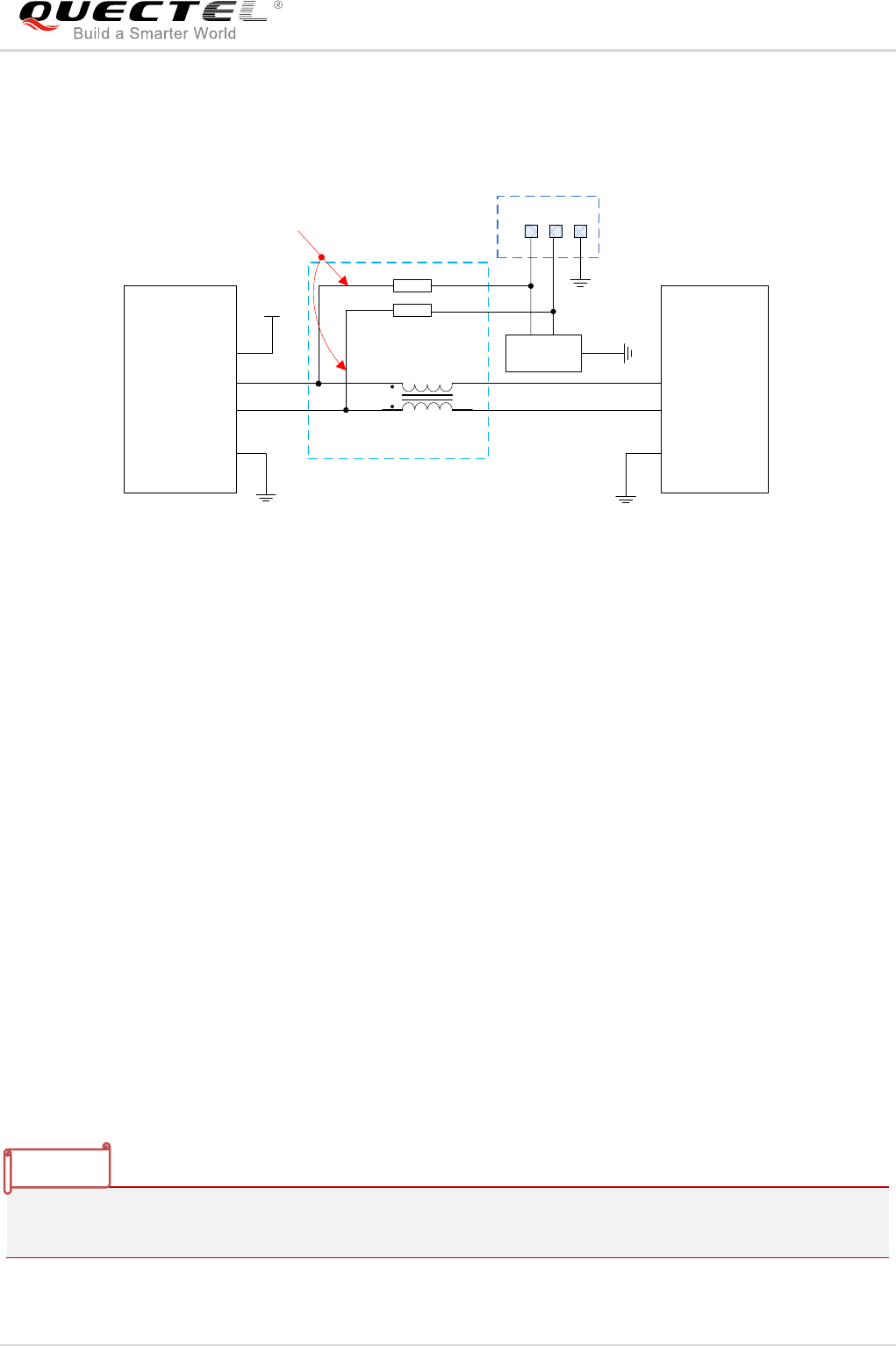
The USB interface is recommended to be reserved for firmware upgrade in customers’ design. The
following figure shows a reference circuit of USB interface.
USB_DP
USB_DM
GND
USB_DP
USB_DM
GND
L1
Close to Module
R3
R4
Test Points
ESD Array
NM_0R
NM_0R
Minimize these stubs
Module MCU
USB_VBUS
VDD
Figure 21: Reference Circuit of USB Interface
A common mode choke L1 is recommended to be added in series between the module and customer’s
MCU in order to suppress EMI spurious transmission. Meanwhile, the 0Ω resistors (R3 and R4) should be
added in series between the module and the test points so as to facilitate debugging, and the resistors are
not mounted by default. In order to ensure the integrity of USB data line signal, L1/R3/R4 components
must be placed close to the module, and also these resistors should be placed close to each other. The
extra stubs of trace must be as short as possible.
The following principles should be complied with when design the USB interface, so as to meet USB 2.0
specification.
It is important to route the USB signal traces as differential pairs with total grounding. The impedance
of USB differential trace is 90Ω.
Do not route signal traces under crystals, oscillators, magnetic devices and RF signal traces. It is
important to route the USB differential traces in inner-layer with ground shielding on not only upper
and lower layers but also right and left sides.
Pay attention to the influence of junction capacitance of ESD protection component on USB data
lines. Typically, the capacitance value should be less than 2pF.
Keep the ESD protection components to the USB connector as close as possible.
1. EG95 module can only be used as a slave device.
2. “*” means under development.
NOTES

LTE Module Series
EG95 Hardware Design
EG95_Hardware_Design 40 / 81
3.11. UART Interfaces
The module provides two UART interfaces: the main UART interface and the debug UART interface. The
following shows their features.
The main UART interface supports 9600bps, 19200bps, 38400bps, 57600bps, 115200bps,
230400bps, 460800bps, 921600bps and 3000000bps baud rates, and the default is 115200bps. The
interface can be used for data transmission and AT command communication.
The debug UART interface supports 115200bps baud rate. It is used for Linux console and log
output.
The following tables show the pin definition of the two UART interfaces.
Table 11: Pin Definition of Main UART Interface
Pin Name
Pin No.
I/O
Description
Comment
RI
39
DO
Ring indicator
1.8V power domain
DCD
38
DO
Data carrier detection
CTS
36
DO
Clear to send
RTS
37
DI
Request to send
DTR
30
DI
Sleep mode control
TXD
35
DO
Transmit data
RXD
34
DI
Receive data
Table 12: Pin Definition of Debug UART Interface
Pin Name
Pin No.
I/O
Description
Comment
DBG_TXD
23
DO
Transmit data
1.8V power domain
DBG_RXD
22
DI
Receive data
1.8V power domain
LTE Module Series
EG95 Hardware Design
EG95_Hardware_Design 41 / 81
The logic levels are described in the following table.
Table 13: Logic Levels of Digital I/O
Parameter
Min.
Max.
Unit
VIL
-0.3
0.6
V
VIH
1.2
2.0
V
VOL
0
0.45
V
VOH
1.35
1.8
V
The module provides 1.8V UART interface. A level translator should be used if customers’ application is
equipped with a 3.3V UART interface. A level translator TXS0108EPWR provided by Texas Instruments is
recommended. The following figure shows a reference design.
VCCA VCCB
OE
A1
A2
A3
A4
A5
A6
A7
A8
GND
B1
B2
B3
B4
B5
B6
B7
B8
VDD_EXT
RI
DCD
RTS
RXD
DTR
CTS
TXD
51K 51K
0.1uF 0.1uF
RI_MCU
DCD_MCU
RTS_MCU
RXD_MCU
DTR_MCU
CTS_MCU
TXD_MCU
VDD_MCU
Translator
Figure 22: Reference Circuit with Translator Chip
Please visit http://www.ti.com for more information.
Another example with transistor translation circuit is shown as below. The circuit design of dotted line
section can refer to the circuit design of solid line section, in terms of both module input and output circuit
design. Please pay attention to the direction of connection.
LTE Module Series
EG95 Hardware Design
EG95_Hardware_Design 42 / 81
MCU/ARM
TXD
RXD
VDD_EXT
10K
VCC_MCU 4.7K
10K
VDD_EXT
TXD
RXD
RTS
CTS
DTR
RI
RTS
CTS
GND
GPIO DCD
Module
GPIO
EINT
VDD_EXT 4.7K
GND
1nF
1nF
Figure 23: Reference Circuit with Transistor Circuit
Transistor circuit solution is not suitable for applications with high baud rates exceeding 460Kbps.
3.12. PCM and I2C Interfaces
EG95 provides one Pulse Code Modulation (PCM) digital interface for audio design, which supports the
following modes and one I2C interface:
Primary mode (short frame synchronization, works as both master and slave)
Auxiliary mode (long frame synchronization, works as master only)
In primary mode, the data is sampled on the falling edge of the PCM_CLK and transmitted on the rising
edge. The PCM_SYNC falling edge represents the MSB. In this mode, the PCM interface supports
256kHz, 512kHz, 1024kHz or 2048kHz PCM_CLK at 8kHz PCM_SYNC, and also supports 4096kHz
PCM_CLK at 16kHz PCM_SYNC.
In auxiliary mode, the data is also sampled on the falling edge of the PCM_CLK and transmitted on the
rising edge. The PCM_SYNC rising edge represents the MSB. In this mode, the PCM interface operates
with a 256kHz, 512kHz, 1024kHz or 2048kHz PCM_CLK and an 8kHz, 50% duty cycle PCM_SYNC.
EG95 supports 16-bit linear data format. The following figures show the primary mode’s timing
relationship with 8KHz PCM_SYNC and 2048KHz PCM_CLK, as well as the auxiliary mode’s timing
relationship with 8KHz PCM_SYNC and 256KHz PCM_CLK.
NOTE
LTE Module Series
EG95 Hardware Design
EG95_Hardware_Design 43 / 81
PCM_CLK
PCM_SYNC
PCM_DOUT
MSB LSB MSB
125us
1 2 256255
PCM_DIN
MSB
LSBMSB
Figure 24: Primary Mode Timing
PCM_CLK
PCM_SYNC
PCM_DOUT
MSB LSB
PCM_DIN
125us
MSB
1 2 3231
LSB
Figure 25: Auxiliary Mode Timing
The following table shows the pin definition of PCM and I2C interfaces which can be applied on audio
codec design.
LTE Module Series
EG95 Hardware Design
EG95_Hardware_Design 44 / 81
Table 14: Pin Definition of PCM and I2C Interfaces
Pin Name
Pin No.
I/O
Description
Comment
PCM_DIN
6
DI
PCM data input
1.8V power domain
PCM_DOUT
7
DO
PCM data output
1.8V power domain
PCM_SYNC
5
IO
PCM data frame
synchronization signal
1.8V power domain
PCM_CLK
4
IO
PCM data bit clock
1.8V power domain
I2C_SCL
40
OD
I2C serial clock
Require an external pull-up to
1.8V
I2C_SDA
41
OD
I2C serial data
Require an external pull-up to
1.8V
Clock and mode can be configured by AT command, and the default configuration is master mode using
short frame synchronization format with 2048KHz PCM_CLK and 8KHz PCM_SYNC. Please refer to
document [2] about AT+QDAI command for details.
The following figure shows a reference design of PCM interface with external codec IC.
PCM_DIN
PCM_DOUT
PCM_SYNC
PCM_CLK
I2C_SCL
I2C_SDA
Module
1.8V
4.7K
4.7K
BCLK
LRCK
DAC
ADC
SCL
SDA
BIAS
MICBIAS
INP
INN
LOUTP
LOUTN
Codec
Figure 26: Reference Circuit of PCM Application with Audio Codec
1. It is recommended to reserve RC (R=22Ω, C=22pF) circuit on the PCM lines, especially for
PCM_CLK.
2. EG95 works as a master device pertaining to I2C interface.
NOTES
LTE Module Series
EG95 Hardware Design
EG95_Hardware_Design 45 / 81
3.13. SPI Interface
SPI interface of EG95 acts as the master only. It provides a duplex, synchronous and serial
communication link with the peripheral devices. It is dedicated to one-to-one connection, without chip
select. Its operation voltage is 1.8V with clock rates up to 50MHz.
The following table shows the pin definition of SPI interface.
Table 15: Pin Definition of SPI Interface
Pin Name
Pin No.
I/O
Description
Comment
SPI_CLK
26
DO
Clock signal of SPI interface
1.8V power domain
SPI_MOSI
27
DO
Master output slave input of SPI
interface
1.8V power domain
SPI_MISO
28
DI
Master input slave output of SPI
interface
1.8V power domain
The following figure shows a reference design of SPI interface with peripherals.
SPI_MISO
SPI_MOSI
SPI_CLK
Module
SPI_CLK
SPI_MISO
SPI_MOSI
Peripherals
Figure 27: Reference Circuit of SPI Interface with Peripherals
3.14. Network Status Indication
The module provides one network indication pin: NETLIGHT. The pin is used to drive a network status
indication LED.
The following tables describe the pin definition and logic level changes of NETLIGHT in different network
status.
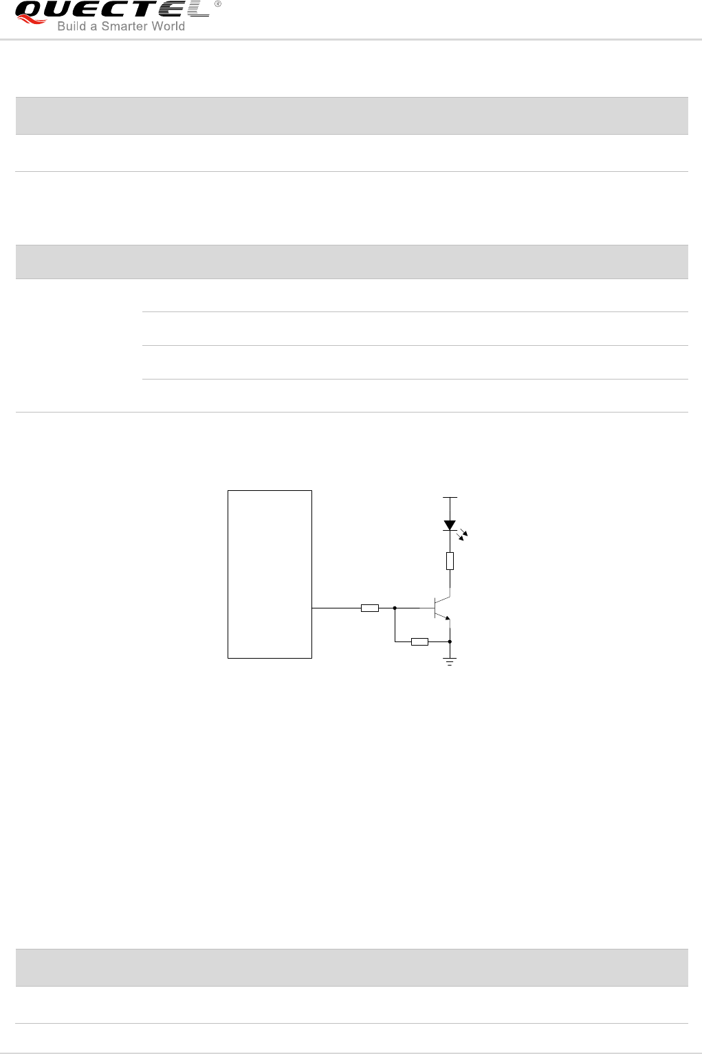
LTE Module Series
EG95 Hardware Design
EG95_Hardware_Design 46 / 81
Table 16: Pin Definition of Network Status Indicator
Pin Name
Pin No.
I/O
Description
Comment
NETLIGHT
21
DO
Indicate the module’s network activity status
1.8V power domain
Table 17: Working State of the Network Status Indicator
Pin Name
Logic Level Changes
Network Status
NETLIGHT
Flicker slowly (200ms High/1800ms Low)
Network searching
Flicker slowly (1800ms High/200ms Low)
Idle
Flicker quickly (125ms High/125ms Low)
Data transfer is ongoing
Always High
Voice calling
A reference circuit is shown in the following figure.
4.7K
47K
VBAT
2.2K
Module
NETLIGHT
Figure 28: Reference Circuit of the Network Status Indicator
3.15. STATUS
The STATUS pin is set as the module status indicator. It will output high level when the module is powered
on. The following table describes the pin definition of STATUS.
Table 18: Pin Definition of STATUS
Pin Name
Pin No.
I/O
Description
Comment
STATUS
20
DO
Indicate the module’s operating status
1.8V power domain
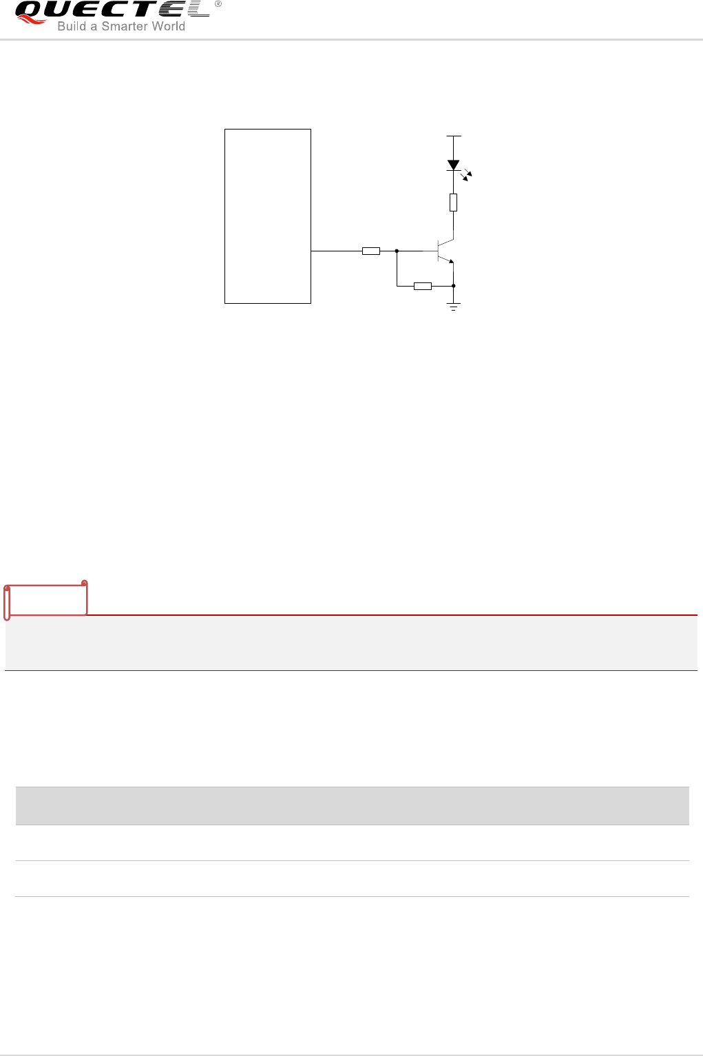
LTE Module Series
EG95 Hardware Design
EG95_Hardware_Design 47 / 81
A reference circuit is shown as below.
4.7K
47K
VBAT
2.2K
Module
STATUS
Figure 29: Reference Circuit of STATUS
3.16. Behaviors of RI
AT+QCFG="risignaltype","physical" command can be used to configure RI behavior.
No matter on which port URC is presented, URC will trigger the behavior of RI pin.
URC can be outputted from UART port, USB AT port and USB modem port through configuration via
AT+QURCCFG command. The default port is USB AT port.
In addition, RI behavior can be configured flexibly. The default behaviors of the RI are shown as below.
Table 19: Default Behaviors of RI
State
Response
Idle
RI keeps at high level
URC
RI outputs 120ms low pulse when a new URC returns
The default RI behaviors can be changed by AT+QCFG="urc/ri/ring" command. Please refer to
document [2] for details.
NOTE

LTE Module Series
EG95 Hardware Design
EG95_Hardware_Design 48 / 81
4 GNSS Receiver
4.1. General Description
EG95 includes a fully integrated global navigation satellite system solution that supports Gen8C-Lite of
Qualcomm (GPS, GLONASS, BeiDou, Galileo and QZSS).
EG95 supports standard NMEA-0183 protocol, and outputs NMEA sentences at 1Hz data update rate via
USB interface by default.
By default, EG95 GNSS engine is switched off. It has to be switched on via AT command. For more
details about GNSS engine technology and configurations, please refer to document [3].
4.2. GNSS Performance
The following table shows GNSS performance of EG95.
Table 20: GNSS Performance
Parameter
Description
Conditions
Typ.
Unit
Sensitivity
(GNSS)
Cold start
Autonomous
TBD
dBm
Reacquisition
Autonomous
TBD
dBm
Tracking
Autonomous
TBD
dBm
TTFF
(GNSS)
Cold start
@open sky
Autonomous
TBD
s
XTRA enabled
TBD
s
Warm start
@open sky
Autonomous
TBD
s
XTRA enabled
TBD
s
Hot start
Autonomous
TBD
s

LTE Module Series
EG95 Hardware Design
EG95_Hardware_Design 49 / 81
@open sky
XTRA enabled
TBD
s
Accuracy
(GNSS)
CEP-50
Autonomous
@open sky
TBD
m
1. Tracking sensitivity: the lowest GNSS signal value at the antenna port on which the module can keep
on positioning for 3 minutes.
2. Reacquisition sensitivity: the lowest GNSS signal value at the antenna port on which the module can
fix position again within 3 minutes after loss of lock.
3. Cold start sensitivity: the lowest GNSS signal value at the antenna port on which the module fixes
position within 3 minutes after executing cold start command.
4.3. Layout Guidelines
The following layout guidelines should be taken into account in customers’ design.
Maximize the distance among GNSS antenna, main antenna and Rx-diversity antenna.
Digital circuits such as (U)SIM card, USB interface, camera module and display connector should be
kept away from the antennas.
Use ground vias around the GNSS trace and sensitive analog signal traces to provide coplanar
isolation and protection.
Keep the characteristic impedance for ANT_GNSS trace as 50Ω.
Please refer to Chapter 5 for GNSS reference design and antenna installation information.
NOTES

LTE Module Series
EG95 Hardware Design
EG95_Hardware_Design 50 / 81
5 Antenna Interfaces
EG95 antenna interfaces include a main antenna interface and an Rx-diversity antenna interface which is
used to resist the fall of signals caused by high speed movement and multipath effect, and a GNSS
antenna interface which is only supported on EG95-NA. The antenna ports have an impedance of 50Ω.
5.1. Main/Rx-diversity Antenna Interfaces
5.1.1. Pin Definition
The pin definition of main antenna and Rx-diversity antenna interfaces is shown below.
Table 21: Pin Definition of RF Antenna
Pin Name
Pin No.
I/O
Description
Comment
ANT_MAIN
60
IO
Main antenna pad
50Ω impedance
ANT_DIV
(EG95-E)
49
AI
Receive diversity antenna pad
50Ω impedance
ANT_DIV
(EG95-NA)
56
AI
Receive diversity antenna pad
50Ω impedance
5.1.2. Operating Frequency
Table 22: Module Operating Frequencies
3GPP Band
Transmit
Receive
Unit
EGSM900
880~915
925~960
MHz
DCS1800
1710~1785
1805~1880
MHz
WCDMA B1
1920~1980
2110~2170
MHz
WCDMA B2
1850~1910
1930~1990
MHz
WCDMA B4
1710~1755
2110~2155
MHz
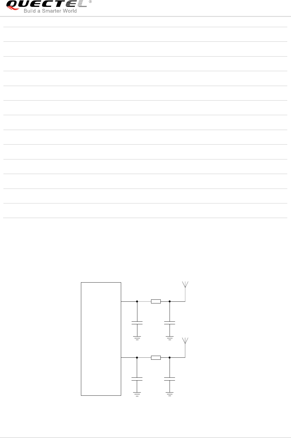
LTE Module Series
EG95 Hardware Design
EG95_Hardware_Design 51 / 81
WCDMA B5
824~849
869~894
MHz
WCDMA B8
880~915
925~960
MHz
LTE-FDD B1
1920~1980
2110~2170
MHz
LTE FDD B2
1850~1910
1930~1990
MHz
LTE-FDD B3
1710~1785
1805~1880
MHz
LTE FDD B4
1710~1755
2110~2155
MHz
LTE FDD B5
824~849
869~894
MHz
LTE-FDD B7
2500~2570
2620~2690
MHz
LTE-FDD B8
880~915
925~960
MHz
LTE FDD B12
699~716
729~746
MHz
LTE FDD B13
777~787
746~756
MHz
LTE-FDD B20
832~862
791~821
MHz
LTE-FDD B28A
703~733
758~788
MHz
5.1.3. Reference Design of RF Antenna Interface
A reference design of ANT_MAIN and ANT_DIV antenna pads is shown as below. A π-type matching
circuit should be reserved for better RF performance. The capacitors are not mounted by default.
ANT_MAIN
R1 0R
C1
Module Main
antenna
NM
C2
NM
R2 0R
C3
Diversity
antenna
NM
C4
NM
ANT_DIV
Figure 30: Reference Circuit of RF Antenna Interface
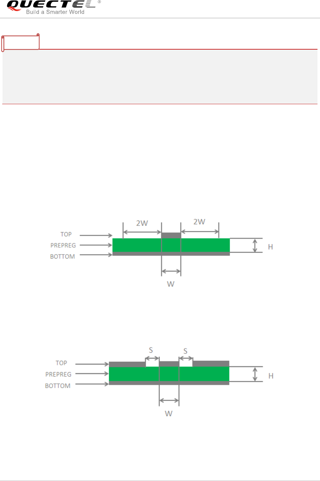
LTE Module Series
EG95 Hardware Design
EG95_Hardware_Design 52 / 81
1. Keep a proper distance between the main antenna and the Rx-diversity antenna to improve the
receiving sensitivity.
2. ANT_DIV function is enabled by default. AT+QCFG="diversity",0 command can be used to disable
receive diversity.
3. Place the π-type matching components (R1/C1/C2, R2/C3/C4) as close to the antenna as possible.
5.1.4. Reference Design of RF Layout
For user’s PCB, the characteristic impedance of all RF traces should be controlled as 50Ω. The
impedance of the RF traces is usually determined by the trace width (W), the materials’ dielectric constant,
the distance between signal layer and reference ground (H), and the clearance between RF trace and
ground (S). Microstrip line or coplanar waveguide line is typically used in RF layout for characteristic
impedance control. The following are reference designs of microstrip line or coplanar waveguide line with
different PCB structures.
.
Figure 31: Microstrip Line Design on a 2-layer PCB
Figure 32: Coplanar Waveguide Line Design on a 2-layer PCB
NOTES
LTE Module Series
EG95 Hardware Design
EG95_Hardware_Design 53 / 81
Figure 33: Coplanar Waveguide Line Design on a 4-layer PCB (Layer 3 as Reference Ground)
Figure 34: Coplanar Waveguide Line Design on a 4-layer PCB (Layer 4 as Reference Ground)
In order to ensure RF performance and reliability, the following principles should be complied with in RF
layout design:
Use impedance simulation tool to control the characteristic impedance of RF traces as 50Ω.
The GND pins adjacent to RF pins should not be designed as thermal relief pads, and should be fully
connected to ground.
The distance between the RF pins and the RF connector should be as short as possible, and all the
right angle traces should be changed to curved ones.
There should be clearance area under the signal pin of the antenna connector or solder joint.
The reference ground of RF traces should be complete. Meanwhile, adding some ground vias around
RF traces and the reference ground could help to improve RF performance. The distance between
the ground vias and RF traces should be no less than two times the width of RF signal traces (2*W).
For more details about RF layout, please refer to document [4].
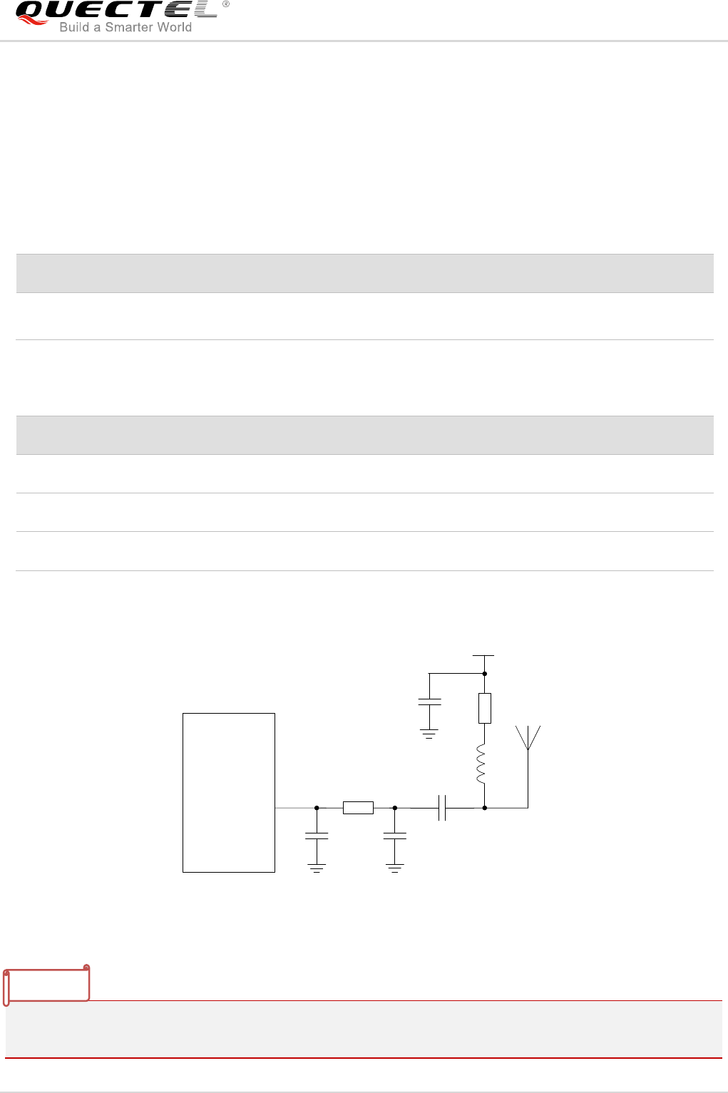
LTE Module Series
EG95 Hardware Design
EG95_Hardware_Design 54 / 81
5.2. GNSS Antenna Interface
The GNSS antenna interface is only supported on EG95-NA.The following tables show pin definition and
frequency specification of GNSS antenna interface.
Table 23: Pin Definition of GNSS Antenna Interface
Pin Name
Pin No.
I/O
Description
Comment
ANT_GNSS
(EG95-NA)
49
AI
GNSS antenna
50Ω impedance
Table 24: GNSS Frequency
Type
Frequency
Unit
GPS/Galileo/QZSS
1575.42±1.023
MHz
GLONASS
1597.5~1605.8
MHz
BeiDou
1561.098±2.046
MHz
A reference design of GNSS antenna is shown as below.
GNSS
Antenna
VDD
Module
ANT_GNSS
47nH
10R
0.1uF
0R
NM NM
100pF
Figure 35: Reference Circuit of GNSS Antenna
1. An external LDO can be selected to supply power according to the active antenna requirement.
2. If the module is designed with a passive antenna, then the VDD circuit is not needed.
NOTES
LTE Module Series
EG95 Hardware Design
EG95_Hardware_Design 55 / 81
5.3. Antenna Installation
5.3.1. Antenna Requirement
The following table shows the requirements on main antenna, Rx-diversity antenna and GNSS antenna.
Table 25: Antenna Requirements
Type
Requirements
GNSS1)
Frequency range: 1561MHz ~ 1615MHz
Polarization: RHCP or linear
VSWR: < 2 (Typ.)
Passive antenna gain: > 0dBi
Active antenna noise figure: < 1.5dB
Active antenna gain: > 0dBi
Active antenna embedded LNA gain: < 17dB
GSM/WCDMA/LTE
VSWR: ≤ 2
Efficiency : > 30%
Max Input Power: 50 W
Input Impedance: 50Ω
Cable insertion loss: < 1dB
(EGSM900,WCDMA B5/B8,
LTE B5/B8/B12/B13/B20/B28A)
Cable Insertion Loss: < 1.5dB
(DCS1800, WCDMA B1/B2/B4, LTE B1/B2/B3/B4)
Cable insertion loss: < 2dB
(LTE B7)
1) It is recommended to use a passive GNSS antenna when LTE B13 or B14 is supported, as the use of
active antenna may generate harmonics which will affect the GNSS performance.
NOTE
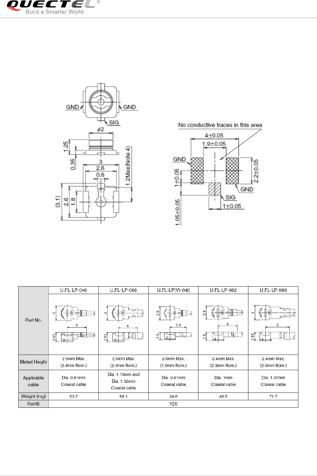
LTE Module Series
EG95 Hardware Design
EG95_Hardware_Design 56 / 81
5.3.2. Recommended RF Connector for Antenna Installation
If RF connector is used for antenna connection, it is recommended to use U.FL-R-SMT connector
provided by HIROSE.
Figure 36: Dimensions of the U.FL-R-SMT Connector (Unit: mm)
U.FL-LP serial connectors listed in the following figure can be used to match the U.FL-R-SMT.
Figure 37: Mechanicals of U.FL-LP Connectors
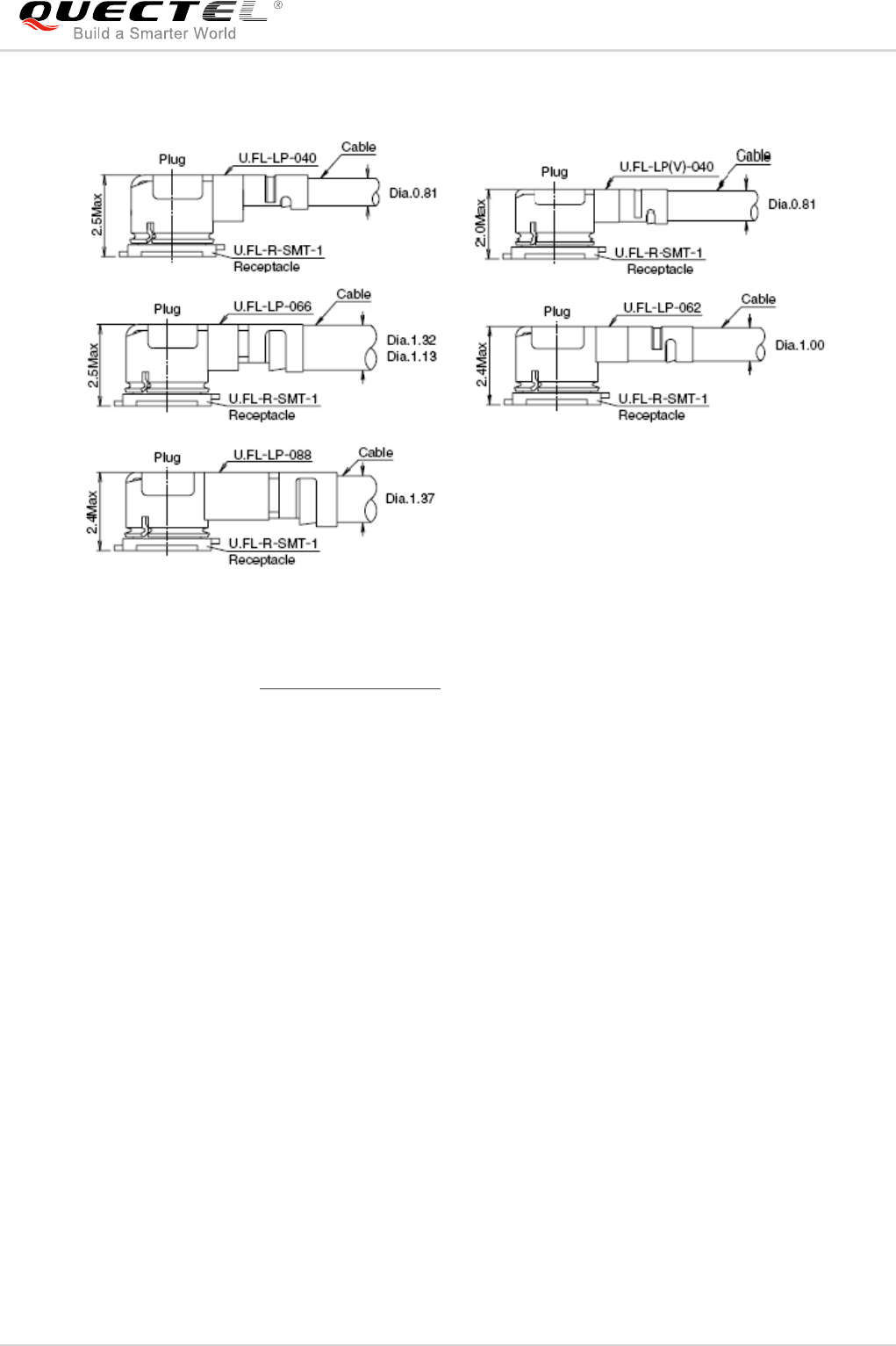

LTE Module Series
EG95 Hardware Design
EG95_Hardware_Design 58 / 81
6 Electrical, Reliability and Radio
Characteristics
6.1. Absolute Maximum Ratings
Absolute maximum ratings for power supply and voltage on digital and analog pins of the module are
listed in the following table.
Table 26: Absolute Maximum Ratings
Parameter
Min.
Max.
Unit
VBAT_RF/VBAT_BB
-0.3
4.7
V
USB_VBUS
-0.3
5.5
V
Peak Current of VBAT_BB
0
0.8
A
Peak Current of VBAT_RF
0
1.8
A
Voltage at Digital Pins
-0.3
2.3
V
6.2. Power Supply Ratings
Table 27: Power Supply Ratings
Parameter
Description
Conditions
Min.
Typ.
Max.
Unit
VBAT
VBAT_BB and
VBAT_RF
The actual input voltages
must stay between the
minimum and maximum
values.
3.3
3.8
4.3
V
LTE Module Series
EG95 Hardware Design
EG95_Hardware_Design 59 / 81
Voltage drop during
burst transmission
Maximum power control
level on EGSM900
400
mV
IVBAT
Peak supply current
(during transmission
slot)
Maximum power control
level on EGSM900
1.8
2.0
A
USB_VBUS
USB connection
detection
3.0
5.0
5.25
V
6.3. Operation and Storage Temperatures
The operation and storage temperatures are listed in the following table.
Table 28: Operation and Storage Temperatures
Parameter
Min.
Typ.
Max.
Unit
Operation Temperature Range 1)
-35
+25
+75
ºC
Extended Temperature Range 2)
-40
+85
ºC
Storage Temperature Range
-40
+90
ºC
1. 1) Within operation temperature range, the module is 3GPP compliant.
2. 2) Within extended temperature range, the module remains the ability to establish and maintain a
voice, SMS, data transmission, emergency call, etc. There is no unrecoverable malfunction. There
are also no effects on radio spectrum and no harm to radio network. Only one or more parameters
like Pout might reduce in their value and exceed the specified tolerances. When the temperature
returns to the normal operating temperature levels, the module will meet 3GPP specifications again.
NOTES

LTE Module Series
EG95 Hardware Design
EG95_Hardware_Design 60 / 81
6.4. Current Consumption
The values of current consumption are shown below.
Table 29: EG95-E Current Consumption
Parameter
Description
Conditions
Typ.
Unit
IVBAT
OFF state
Power down
15
uA
Sleep state
AT+CFUN=0 (USB disconnected)
1.3
mA
GSM DRX=2 (USB disconnected)
2.3
mA
GSM DRX=5 (USB suspend)
2.0
mA
GSM DRX=9 (USB disconnected)
1.6
mA
WCDMA PF=64 (USB disconnected)
1.8
mA
WCDMA PF=64 (USB suspend)
2.1
mA
WCDMA PF=512 (USB disconnected)
1.3
mA
LTE-FDD PF=64 (USB disconnected)
2.3
mA
LTE-FDD PF=64 (USB suspend)
2.6
mA
LTE-FDD PF=256 (USB disconnected)
1.5
mA
Idle state
GSM DRX=5 (USB disconnected)
21.0
mA
GSM DRX=5 (USB connected)
31.0
mA
WCDMA PF=64 (USB disconnected)
21.0
mA
WCDMA PF=64 (USB connected)
31.0
mA
LTE-FDD PF=64 (USB disconnected)
21.0
mA
LTE-FDD PF=64 (USB connected)
31.0
mA
GPRS data
transfer
EGSM900 4DL/1UL @32.35dBm
268
mA
EGSM900 3DL/2UL @32.16dBm
459
mA
EGSM900 2DL/3UL @30.57dBm
547
mA

LTE Module Series
EG95 Hardware Design
EG95_Hardware_Design 61 / 81
EGSM900 1DL/4UL @29.45dBm
631
mA
DCS1800 4DL/1UL @29.14dBm
177
mA
DCS1800 3DL/2UL @29.07dBm
290
mA
DCS1800 2DL/3UL @28.97dBm
406
mA
DCS1800 1DL/4UL @28.88dBm
517
mA
EDGE data
transfer
EGSM900 4DL/1UL PCL=8 @26.88dBm
167
mA
EGSM900 3DL/2UL PCL=8 @26.84dBm
278
mA
EGSM900 2DL/3UL PCL=8 @26.76dBm
385
mA
EGSM900 1DL/4UL PCL=8 @26.54dBm
492
mA
DCS1800 4DL/1UL PCL=2 @25.66dBm
169
mA
DCS1800 3DL/2UL PCL=2 @25.59dBm
256
mA
DCS1800 2DL/3UL PCL=2 @25.51dBm
341
mA
DCS1800 1DL/4UL PCL=2 @25.38dBm
432
mA
WCDMA data
transfer
WCDMA B1 HSDPA @22.48dBm
586
mA
WCDMA B1 HSUPA @22.29dBm
591
mA
WCDMA B8 HSDPA @22.24dBm
498
mA
WCDMA B8 HSUPA @21.99dBm
511
mA
LTE data
transfer
LTE-FDD B1 @23.37dBm
736
mA
LTE-FDD B3 @22.97dBm
710
mA
LTE-FDD B7 @23.17dBm
775
mA
LTE-FDD B8 @23.04dBm
651
mA
LTE-FDD B20 @23.21dBm
699
mA
LTE-FDD B28A @22.76dBm
714
mA
GSM
voice call
EGSM900 PCL=5 @32.36dBm
271
mA
DCS1800 PCL=0 @29.19dBm
181
mA

LTE Module Series
EG95 Hardware Design
EG95_Hardware_Design 62 / 81
WCDMA
voice call
WCDMA B1 @22.91dBm
632
mA
WCDMA B8 @23.14dBm
546
mA
Table 30: EG95-NA Current Consumption
Parameter
Description
Conditions
Typ.
Unit
IVBAT
OFF state
Power down
TBD
uA
Sleep state
AT+CFUN=0 (USB disconnected)
TBD
mA
WCDMA PF=64 (USB disconnected)
TBD
mA
WCDMA PF=64 (USB suspend)
TBD
mA
WCDMA PF=512 (USB disconnected)
TBD
mA
LTE-FDD PF=64 (USB disconnected)
TBD
mA
LTE-FDD PF=64 (USB suspend)
TBD
mA
LTE-FDD PF=256 (USB disconnected)
TBD
mA
Idle state
WCDMA PF=64 (USB disconnected)
TBD
mA
WCDMA PF=64 (USB connected)
TBD
mA
LTE-FDD PF=64 (USB disconnected)
TBD
mA
LTE-FDD PF=64 (USB connected)
TBD
mA
WCDMA data
transfer
WCDMA B2 HSDPA @ TBD dBm
TBD
mA
WCDMA B2 HSUPA @ TBD dBm
TBD
mA
WCDMA B4 HSDPA @ TBD dBm
TBD
mA
WCDMA B4 HSUPA @ TBD dBm
TBD
mA
WCDMA B5 HSDPA @ TBD dBm
TBD
mA
WCDMA B5 HSUPA @ TBD dBm
TBD
mA
LTE data
transfer
LTE-FDD B2 @ TBD dBm
TBD
mA
LTE-FDD B4 @ TBD dBm
TBD
mA
LTE Module Series
EG95 Hardware Design
EG95_Hardware_Design 63 / 81
LTE-FDD B5 @ TBD dBm
TBD
mA
LTE-FDD B12 @ TBD dBm
TBD
mA
LTE-FDD B13 @ TBD dBm
TBD
mA
WCDMA
voice call
WCDMA B2 @ TBD dBm
TBD
mA
WCDMA B4 @ TBD dBm
TBD
mA
WCDMA B5 @ TBD dBm
TBD
mA
Table 31: GNSS Current Consumption of EG95-NA
6.5. RF Output Power
The following table shows the RF output power of EG95 module.
Table 32: RF Output Power
Frequency
Max.
Min.
EGSM900
33dBm±2dB
5dBm±5dB
DCS1800
30dBm±2dB
0dBm±5dB
EGSM900 (8-PSK)
27dBm±3dB
5dBm±5dB
DCS1800 (8-PSK)
26dBm±3dB
0dBm±5dB
WCDMA B1/B2/B4/B5/B8
24dBm+1/-3dB
<-49dBm
Parameter
Description
Conditions
Typ.
Unit
IVBAT
(GNSS)
Searching
(AT+CFUN=0)
Cold start @Passive Antenna
TBD
mA
Lost state @Passive Antenna
TBD
mA
Tracking
(AT+CFUN=0)
Instrument Environment
TBD
mA
Open Sky @Passive Antenna
TBD
mA
Open Sky @Active Antenna
TBD
mA
LTE Module Series
EG95 Hardware Design
EG95_Hardware_Design 64 / 81
LTE-FDD B1/B2/B3/B4/B5/B7/
B8/B12/B13/B20/B28A
23dBm±2dB
<-39dBm
In GPRS 4 slots TX mode, the maximum output power is reduced by 3.0dB. The design conforms to the
GSM specification as described in Chapter 13.16 of 3GPP TS 51.010-1.
6.6. RF Receiving Sensitivity
The following tables show the conducted RF receiving sensitivity of EG95 module.
Table 33: EG95-E Conducted RF Receiving Sensitivity
Frequency
Primary
Diversity
SIMO
3GPP
EGSM900
-108.6dBm
NA
NA
-102dBm
DCS1800
-109.4 dBm
NA
NA
-102dbm
WCDMA B1
-109.5dBm
-110dBm
-112.5dBm
-106.7dBm
WCDMA B8
-109.5dBm
-110dBm
-112.5dBm
-103.7dBm
LTE-FDD B1 (10M)
-97.5dBm
-98.3dBm
-101.4dBm
-96.3dBm
LTE-FDD B3 (10M)
-98.3dBm
-98.5dBm
-101.5dBm
-93.3dBm
LTE-FDD B7 (10M)
-96.3dBm
-98.4dBm
-101.3dBm
-94.3dBm
LTE-FDD B8 (10M)
-97.1dBm
-99.1dBm
-101.2dBm
-93.3dBm
LTE-FDD B20 (10M)
-97dBm
-99dBm
-101.3dBm
-93.3dBm
LTE-FDD B28A (10M)
-98.3dBm
-99dBm
-101.4dBm
-94.8dBm
NOTE

LTE Module Series
EG95 Hardware Design
EG95_Hardware_Design 65 / 81
Table 34: EG95-NA Conducted RF Receiving Sensitivity
Frequency
Primary
Diversity
SIMO
3GPP
WCDMA B2
TBD
TBD
TBD
-104.7dBm
WCDMA B4
TBD
TBD
TBD
-106.7dBm
WCDMA B5
TBD
TBD
TBD
-104.7dBm
LTE-FDD B2 (10M)
TBD
TBD
TBD
-94.3dBm
LTE-FDD B4 (10M)
TBD
TBD
TBD
-96.3dBm
LTE-FDD B5 (10M)
TBD
TBD
TBD
-94.3dBm
LTE-FDD B12 (10M)
TBD
TBD
TBD
-93.3dBm
LTE-FDD B13 (10M)
TBD
TBD
TBD
-93.3dBm
6.7. Electrostatic Discharge
The module is not protected against electrostatic discharge (ESD) in general. Consequently, it is subject
to ESD handling precautions that typically apply to ESD sensitive components. Proper ESD handling and
packaging procedures must be applied throughout the processing, handling and operation of any
application that incorporates the module.
The following table shows the module’s electrostatic discharge characteristics.
Table 35: Electrostatic Discharge Characteristics
Tested Points
Contact Discharge
Air Discharge
Unit
VBAT, GND
±5
±10
KV
All Antenna Interfaces
±4
±8
KV
Other Interfaces
±0.5
±1
KV
LTE Module Series
EG95 Hardware Design
EG95_Hardware_Design 66 / 81
6.8. Thermal Consideration
In order to achieve better performance of the module, it is recommended to comply with the following
principles for thermal consideration:
On customers’ PCB design, please keep placement of the module away from heating sources,
especially high power components such as ARM processor, audio power amplifier, power supply, etc.
Do not place components on the opposite side of the PCB area where the module is mounted, in
order to facilitate adding of heatsink when necessary.
Do not apply solder mask on the opposite side of the PCB area where the module is mounted, so as
to ensure better heat dissipation performance.
The reference ground of the area where the module is mounted should be complete, and add ground
vias as many as possible for better heat dissipation.
Make sure the ground pads of the module and PCB are fully connected.
According to customers’ application demands, the heatsink can be mounted on the top of the module,
or the opposite side of the PCB area where the module is mounted, or both of them.
The heatsink should be designed with as many fins as possible to increase heat dissipation area.
Meanwhile, a thermal pad with high thermal conductivity should be used between the heatsink and
module/PCB.
The size of the heatsink should be larger than that of the module’s shielding cover to avoid the
deformation of the shielding cover.
The following shows two kinds of heatsink designs for reference and customers can choose one or both
of them according to their application structure.
Heatsink
EG95 Module
Application Board Application Board
Heatsink
Thermal Pad
Shielding Cover
Figure 39: Referenced Heatsink Design (Heatsink at the Top of the Module)
LTE Module Series
EG95 Hardware Design
EG95_Hardware_Design 67 / 81
Thermal Pad
Heatsink
Application Board Application Board
Heatsink
Thermal Pad
EG95 Module
Shielding Cover
Figure 40: Referenced Heatsink Design (Heatsink at the Bottom of Customers’ PCB)
The module offers the best performance when the internal BB chip stays below 105°C. When the
maximum temperature of the BB chip reaches or exceeds 105°C, the module works normal but provides
reduced performance (such as RF output power, data rate, etc.). When the maximum BB chip
temperature reaches or exceeds 115°C, the module will disconnect from the network, and it will recover to
network connected state after the maximum temperature falls below 115°C. Therefore, the thermal design
should be maximally optimized to make sure the maximum BB chip temperature always maintains below
105°C. Customers can execute AT+QTEMP command and get the maximum BB chip temperature from
the first returned value.
NOTE
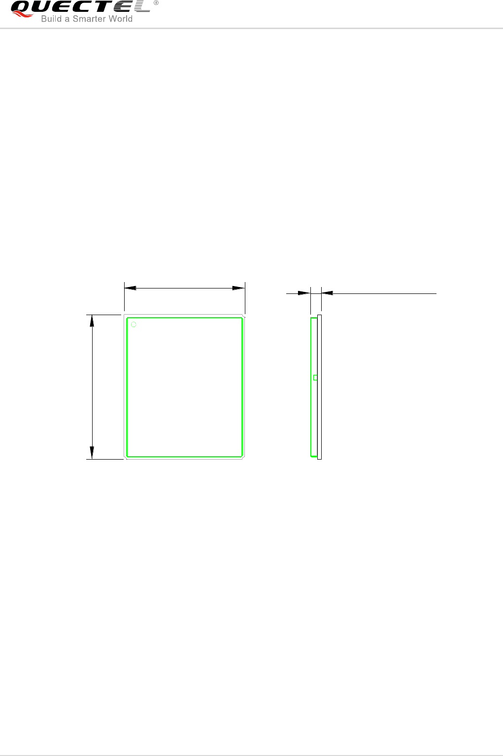
LTE Module Series
EG95 Hardware Design
EG95_Hardware_Design 68 / 81
7 Mechanical Dimensions
This chapter describes the mechanical dimensions of the module. All dimensions are measured in mm.
The tolerances for dimensions without tolerance values are ±0.05mm.
7.1. Mechanical Dimensions of the Module
25±0.15
29±0.15
2.25±0.2
Figure 41: Module Top and Side Dimensions
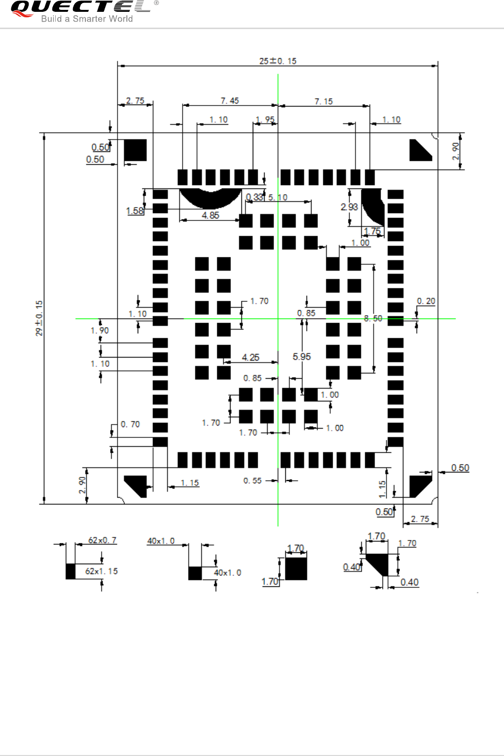
LTE Module Series
EG95 Hardware Design
EG95_Hardware_Design 69 / 81
Figure 42: Module Bottom Dimensions (Top View)
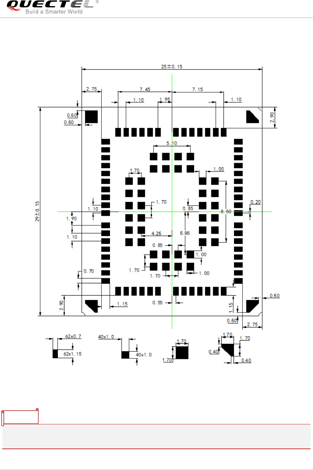
LTE Module Series
EG95 Hardware Design
EG95_Hardware_Design 70 / 81
7.2. Recommended Footprint
Figure 43: Recommended Footprint (Top View)
For easy maintenance of the module, please keep about 3mm between the module and other
components in the host PCB.
NOTE
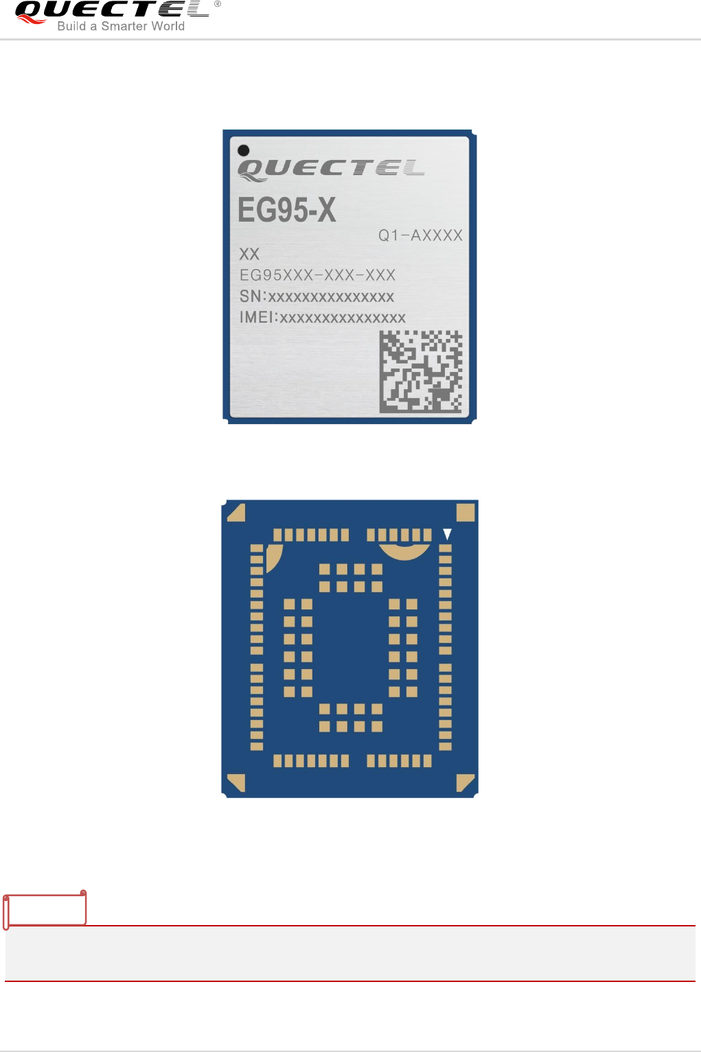
LTE Module Series
EG95 Hardware Design
EG95_Hardware_Design 71 / 81
7.3. Design Effect Drawings of the Module
Figure 44: Top View of the Module
Figure 45: Bottom View of the Module
These are design effect drawings of EG95 module. For more accurate pictures, please refer to the
module that you get from Quectel.
NOTE
LTE Module Series
EG95 Hardware Design
EG95_Hardware_Design 72 / 81
8 Storage, Manufacturing and
Packaging
8.1. Storage
EG95 is stored in a vacuum-sealed bag. The storage restrictions are shown as below.
1. Shelf life in the vacuum-sealed bag: 12 months at <40ºC/90%RH.
2. After the vacuum-sealed bag is opened, devices that will be subjected to reflow soldering or other
high temperature processes must be:
Mounted within 168 hours at the factory environment of ≤30ºC/60%RH.
Stored at <10%RH.
3. Devices require baking before mounting, if any circumstance below occurs.
When the ambient temperature is 23ºC±5ºC and the humidity indication card shows the humidity
is >10% before opening the vacuum-sealed bag.
Device mounting cannot be finished within 168 hours at factory conditions of ≤30ºC/60%RH.
4. If baking is required, devices may be baked for 8 hours at 120ºC±5ºC.
As the plastic package cannot be subjected to high temperature, it should be removed from devices
before high temperature (120ºC ) baking. If shorter baking time is desired, please refer to
IPC/JEDECJ-STD-033 for baking procedure.
NOTE
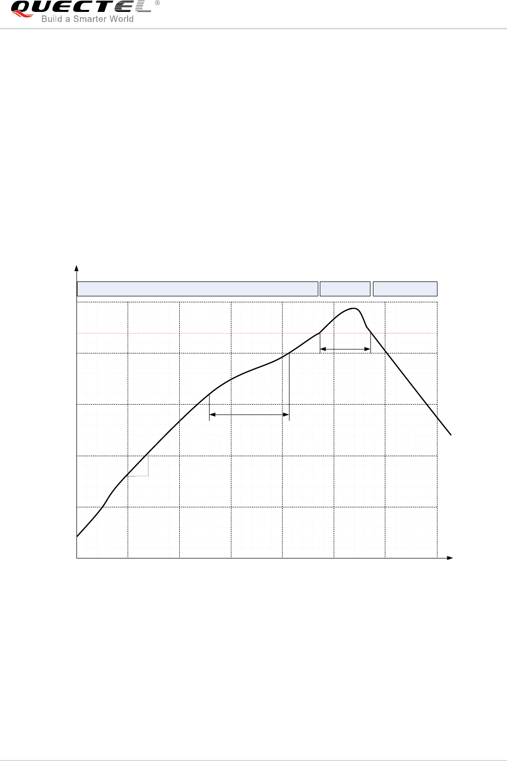
LTE Module Series
EG95 Hardware Design
EG95_Hardware_Design 73 / 81
8.2. Manufacturing and Soldering
Push the squeegee to apply the solder paste on the surface of stencil, thus making the paste fill the
stencil openings and then penetrate to the PCB. The force on the squeegee should be adjusted properly
so as to produce a clean stencil surface on a single pass. To ensure the module soldering quality, the
thickness of stencil for the module is recommended to be 0.18mm. For more details, please refer to
document [3].
It is suggested that the peak reflow temperature is 235ºC~245ºC (for SnAg3.0Cu0.5 alloy). The absolute
maximum reflow temperature is 260ºC. To avoid damage to the module caused by repeated heating, it is
suggested that the module should be mounted after reflow soldering for the other side of PCB has been
completed. Recommended reflow soldering thermal profile is shown below:
Time
50 100 150 200 250 300
50
100
150
200
250
160 ºC
200 ºC
217
0
70s~120s
40s~60s
Between 1~3 ºC/s
Preheat Heating Cooling
ºC
s
Liquids Temperature
Temperature
Figure 46: Reflow Soldering Thermal Profile
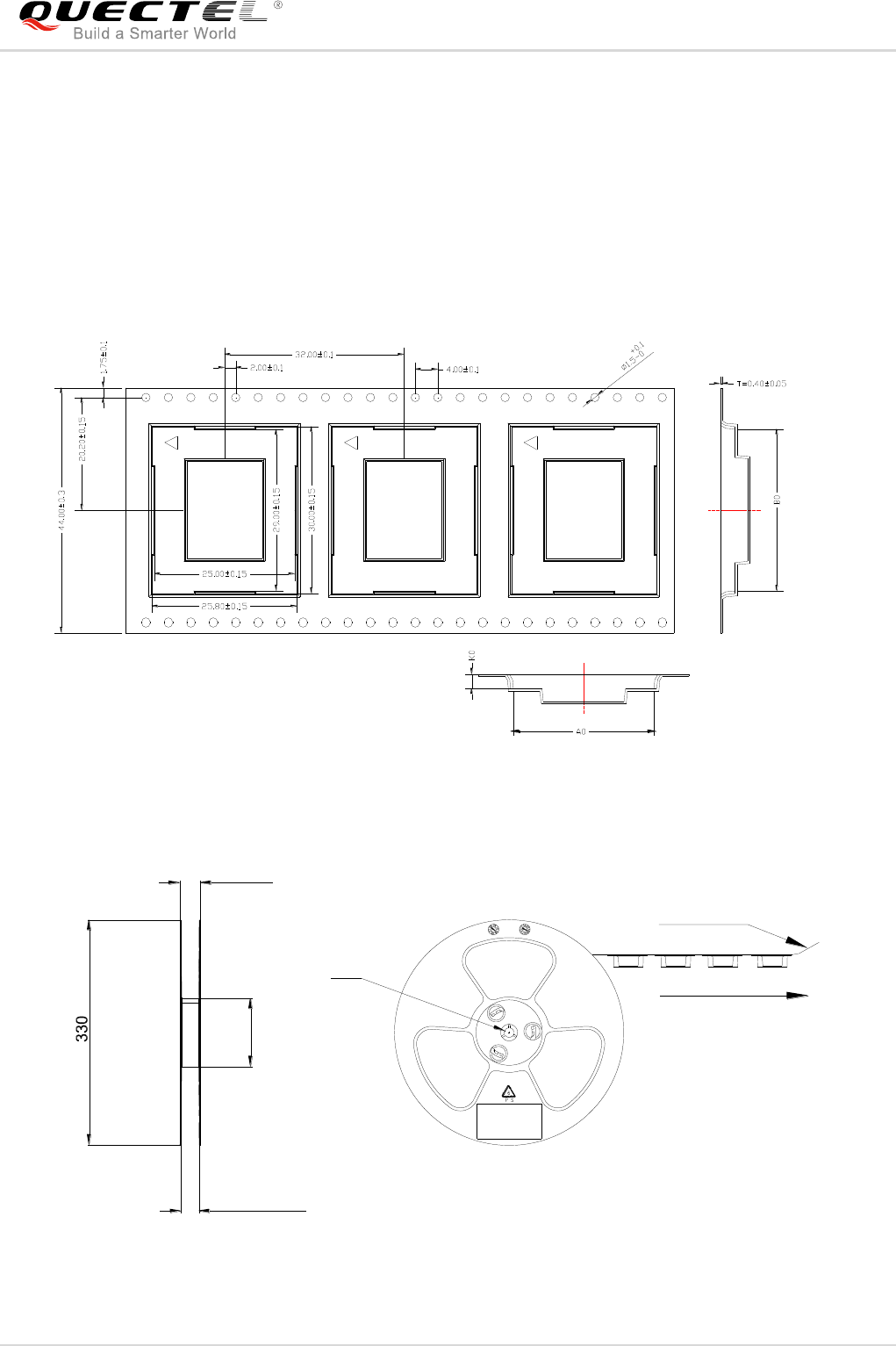
LTE Module Series
EG95 Hardware Design
EG95_Hardware_Design 74 / 81
8.3. Packaging
EG95 is packaged in a vacuum-sealed bag which is ESD protected. The bag should not be opened until
the devices are ready to be soldered onto the application.
The reel is 330mm in diameter and each reel contains 250pcs modules. The following figures show the
packaging details, measured in mm.
Figure 47: Tape Dimensions
Direction of feed
Cover tape
13
100
44.5+0.20
-0.00
48.5
Figure 48: Reel Dimensions
LTE Module Series
EG95 Hardware Design
EG95_Hardware_Design 75 / 81
9 Appendix A References
Table 36: Related Documents
SN
Document Name
Remark
[1]
Quectel_EC2x&EG9x&EM05_Power_Management_
Application_Note
Power Management Application Note
for EC25, EC21, EC20 R2.0, EC20
R2.1, EG95, EG91 and EM05
[2]
Quectel_EG9x_AT_Commands_Manual
AT Commands Manual for EG95 and
EG91
[3]
Quectel_Module_Secondary_SMT_User_Guide
Module Secondary SMT User Guide
[4]
Quectel_RF_Layout_Application_Note
RF Layout Application Note
Table 37: Terms and Abbreviations
Abbreviation
Description
AMR
Adaptive Multi-rate
bps
Bits Per Second
CHAP
Challenge Handshake Authentication Protocol
CS
Coding Scheme
CSD
Circuit Switched Data
CTS
Clear To Send
DC-HSPA+
Dual-carrier High Speed Packet Access
DFOTA
Delta Firmware Upgrade Over The Air
DL
Downlink
DTR
Data Terminal Ready
DTX
Discontinuous Transmission

LTE Module Series
EG95 Hardware Design
EG95_Hardware_Design 76 / 81
EFR
Enhanced Full Rate
ESD
Electrostatic Discharge
FDD
Frequency Division Duplex
FR
Full Rate
GMSK
Gaussian Minimum Shift Keying
GSM
Global System for Mobile Communications
HR
Half Rate
HSPA
High Speed Packet Access
HSDPA
High Speed Downlink Packet Access
HSUPA
High Speed Uplink Packet Access
I/O
Input/Output
Inorm
Normal Current
LED
Light Emitting Diode
LNA
Low Noise Amplifier
LTE
Long Term Evolution
MIMO
Multiple Input Multiple Output
MO
Mobile Originated
MS
Mobile Station (GSM engine)
MT
Mobile Terminated
PAP
Password Authentication Protocol
PCB
Printed Circuit Board
PDU
Protocol Data Unit
PPP
Point-to-Point Protocol
QAM
Quadrature Amplitude Modulation
QPSK
Quadrature Phase Shift Keying

LTE Module Series
EG95 Hardware Design
EG95_Hardware_Design 77 / 81
RF
Radio Frequency
RHCP
Right Hand Circularly Polarized
Rx
Receive
SMS
Short Message Service
TDD
Time Division Duplexing
TX
Transmitting Direction
UL
Uplink
UMTS
Universal Mobile Telecommunications System
URC
Unsolicited Result Code
(U)SIM
(Universal) Subscriber Identity Module
Vmax
Maximum Voltage Value
Vnorm
Normal Voltage Value
Vmin
Minimum Voltage Value
VIHmax
Maximum Input High Level Voltage Value
VIHmin
Minimum Input High Level Voltage Value
VILmax
Maximum Input Low Level Voltage Value
VILmin
Minimum Input Low Level Voltage Value
VImax
Absolute Maximum Input Voltage Value
VImin
Absolute Minimum Input Voltage Value
VOax
Maximum Output High Level Voltage Value
VOin
Minimum Output High Level Voltage Value
VOLmax
Maximum Output Low Level Voltage Value
VOLmin
Minimum Output Low Level Voltage Value
VSWR
Voltage Standing Wave Ratio
WCDMA
Wideband Code Division Multiple Access
LTE Module Series
EG95 Hardware Design
EG95_Hardware_Design 78 / 81
10 Appendix B GPRS Coding Schemes
Table 38: Description of Different Coding Schemes
Scheme
CS-1
CS-2
CS-3
CS-4
Code Rate
1/2
2/3
3/4
1
USF
3
3
3
3
Pre-coded USF
3
6
6
12
Radio Block excl.USF and BCS
181
268
312
428
BCS
40
16
16
16
Tail
4
4
4
-
Coded Bits
456
588
676
456
Punctured Bits
0
132
220
-
Data Rate Kb/s
9.05
13.4
15.6
21.4

LTE Module Series
EG95 Hardware Design
EG95_Hardware_Design 79 / 81
11 Appendix C GPRS Multi-slot Classes
Twenty-nine classes of GPRS multi-slot modes are defined for MS in GPRS specification. Multi-slot
classes are product dependent, and determine the maximum achievable data rates in both the uplink and
downlink directions. Written as 3+1 or 2+2, the first number indicates the amount of downlink timeslots,
while the second number indicates the amount of uplink timeslots. The active slots determine the total
number of slots the GPRS device can use simultaneously for both uplink and downlink communications.
The description of different multi-slot classes is shown in the following table.
Table 39: GPRS Multi-slot Classes
Multislot Class
Downlink Slots
Uplink Slots
Active Slots
1
1
1
2
2
2
1
3
3
2
2
3
4
3
1
4
5
2
2
4
6
3
2
4
7
3
3
4
8
4
1
5
9
3
2
5
10
4
2
5
11
4
3
5
12
4
4
5
13
3
3
NA
14
4
4
NA

LTE Module Series
EG95 Hardware Design
EG95_Hardware_Design 80 / 81
15
5
5
NA
16
6
6
NA
17
7
7
NA
18
8
8
NA
19
6
2
NA
20
6
3
NA
21
6
4
NA
22
6
4
NA
23
6
6
NA
24
8
2
NA
25
8
3
NA
26
8
4
NA
27
8
4
NA
28
8
6
NA
29
8
8
NA
30
5
1
6
31
5
2
6
32
5
3
6
33
5
4
6

LTE Module Series
EG95 Hardware Design
EG95_Hardware_Design 81 / 81
12 Appendix D EDGE Modulation and
Coding Schemes
Table 40: EDGE Modulation and Coding Schemes
Coding Scheme
Modulation
Coding Family
1 Timeslot
2 Timeslot
4 Timeslot
CS-1:
GMSK
/
9.05kbps
18.1kbps
36.2kbps
CS-2:
GMSK
/
13.4kbps
26.8kbps
53.6kbps
CS-3:
GMSK
/
15.6kbps
31.2kbps
62.4kbps
CS-4:
GMSK
/
21.4kbps
42.8kbps
85.6kbps
MCS-1
GMSK
C
8.80kbps
17.60kbps
35.20kbps
MCS-2
GMSK
B
11.2kbps
22.4kbps
44.8kbps
MCS-3
GMSK
A
14.8kbps
29.6kbps
59.2kbps
MCS-4
GMSK
C
17.6kbps
35.2kbps
70.4kbps
MCS-5
8-PSK
B
22.4kbps
44.8kbps
89.6kbps
MCS-6
8-PSK
A
29.6kbps
59.2kbps
118.4kbps
MCS-7
8-PSK
B
44.8kbps
89.6kbps
179.2kbps
MCS-8
8-PSK
A
54.4kbps
108.8kbps
217.6kbps
MCS-9
8-PSK
A
59.2kbps
118.4kbps
236.8kbps
FCC Certification Requirements.
According to the definition of mobile and fixed device is described in Part 2.1091(b), this
device is a mobile device.
And the following conditions must be met:
1. This Modular Approval is limited to OEM installation for mobile and fixed applications
only. The antenna installation and operating configurations of this transmitter, including
any applicable source-based time- averaging duty factor, antenna gain and cable loss
must satisfy MPE categorical Exclusion Requirements of 2.1091.
2. The EUT is a mobile device; maintain at least a 20 cm separation between the EUT and
the user’s body and must not transmit simultaneously with any other antenna or
transmitter.
3.A label with the following statements must be attached to the host end product: This
device contains FCC ID: XMR2010E*1A.
4.To comply with FCC regulations limiting both maximum RF output power and human
exposure to RF radiation, maximum antenna gain (including cable loss) must not
exceed:
WCDMA/LTE: <4dBi
5. This module must not transmit simultaneously with any other antenna or
transmitter
6. The host end product must include a user manual that clearly defines operating
requirements and conditions that must be observed to ensure compliance with current
FCC RF exposure guidelines.
For portable devices, in addition to the conditions 3 through 6 described above, a
separate approval is required to satisfy the SAR requirements of FCC Part 2.1093
If the device is used for other equipment that separate approval is required for all other
operating configurations, including portable configurations with respect to 2.1093 and
different antenna configurations.
For this device, OEM integrators must be provided with labeling instructions of finished
products. Please refer to KDB784748 D01 v07, section 8. Page 6/7 last two
paragraphs:
A certified modular has the option to use a permanently affixed label, or an electronic
label. For a permanently affixed label, the module must be labelled withan FCC ID -
Section 2.926 (see 2.2 Certification (labelling requirements) above). The OEM manual
must provide clear instructions explaining to the OEM the labelling
requirements,options and OEM user manual instructions that are required (see next
paragraph).
For a host using a certified modular with a standard fixed label, if (1) the module’s FCC
ID is notvisible when installed in the host, or (2) if the host is marketed so that end users
do not havestraightforward commonly used methods for access to remove the module
so that the FCC ID ofthe module is visible; then an additional permanent label referring
to the enclosed module:“Contains Transmitter Module FCC ID:;05(*1$” or
“Contains FCC ID: XMR201807EG95NA” mustbe used. The host OEM user manual must
also contain clear instructions on how end users can find and/or access the module and
the FCC ID.
The final host / module combination may also need to be evaluated against the FCC
Part 15B criteria for unintentional radiators in order to be properly authorized for
operation as a Part 15 digital device.
The user’s manual or instruction manual for an intentional or unintentional radiator shall
caution the user that changes or modifications not expressly approved by the party
responsible for compliance could void the user's authority to operate the equipment. In
cases where the manual is provided only in a form other than paper, such as on a
computer disk or over the Internet, the information required by this section may be
included in the manual in that alternative form, provided the user can reasonably be
expected to have the capability to access information in that form.
This device complies with part 15 of the FCC Rules. Operation is subject to the
following two conditions: (1) This device may not cause harmful interference, and (2)
this device must accept any interference received, including interference that may
cause undesired operation.
Changes or modifications not expressly approved by the manufacturer could void the
user’s authority to operate the equipment.
To ensure compliance with all non-transmitter functions the host manufacturer is
responsible for ensuring compliance with the module(s) installed and fully operational. For
example, if a host was previously authorized as an unintentional radiator under the
Declaration of Conformity procedure without a transmitter certified module and a module
is added, the host manufacturer is responsible for ensuring that the after the module is
installed and operational the host continues to be compliant with the Part 15B
unintentional radiator requirements.
The host product shall be properly labelled to identify the modules within the host
product.
The Innovation, Science and Economic Development Canada certification label of a
module shall be clearly visible at all times when installed in the host product; otherwise,
the host product must be labelled to display the Innovation, Science and Economic
Development Canada certification number for the module, preceded by the word
“Contains” or similar wording expressing the same meaning, as follows:
“Contains IC: 10224A-2018EG95NA” or “where: 10224A-2018EG95NA is the module’s
certification number”.
Le produit hôte doit être correctement étiqueté pour identifier les modules dans le produit hôte.
L'étiquette de certification d'Innovation, Sciences et Développement économique Canada d'un
module doit être clairement visible en tout temps lorsqu'il est installé dans le produit hôte; sinon,
le produit hôte doit porter une étiquette indiquant le numéro de certification d'Innovation,
Sciences et Développement économique Canada pour le module, précédé du mot «Contient» ou
d'un libellé semblable exprimant la même signification, comme suit:
"Contient IC: 10224A-2018EG95NA" ou "où: 10224A-2018EG95NA est le numéro de certification
du module".
A label with the following statements must be attached to the host end product: This device
contains IC:10224A-2018EG95NA.
The manual provides guidance to the host manufacturer will be included in the documentation
that will be provided to the OEM.
The module is limited to installation in mobile or fixed applications.
The separate approval is required for all other operating configurations, including portable
configurations and different antenna configurations.
The OEM integrators are responsible for ensuring that the end-user has no manual or instructions
to remove or install module.
The module is limited to OEM installation ONLY.
Une étiquette avec les instructions suivantes doit être attachée au produit final hôte:
Cet appareil contient IC: 10224A-2018EG95NA.
Le manuel fournit des conseils au fabricant hôte sera inclus dans la documentation qui sera
fournie à l'OEM.
Le module est limité à l'installation dans des applications mobiles ou fixes.
L'approbation distincte est requise pour toutes les autres configurations de fonctionnement, y
compris les configurations portables et différentes configurations d'antenne.
Les intégrateurs OEM sont responsables de s'assurer que l'utilisateur n'a pas de manuel ou
d'instructions pour retirer ou installer le module.
Le module est limité à l'installation OEM SEULEMENT.