RF Technology 1UTR800CN UHF BASE STATION User Manual R800 Manual
RF Technology Pty Ltd UHF BASE STATION R800 Manual
UserManual.wiki
>
RF Technology
>
1UTR800CN User Manual
Users Manual
Navigation menu
Upload a User Manual
Namespaces
Wiki Guide
HTML
PDF
Info
Views
User Manual
Discussion / Help
Navigation
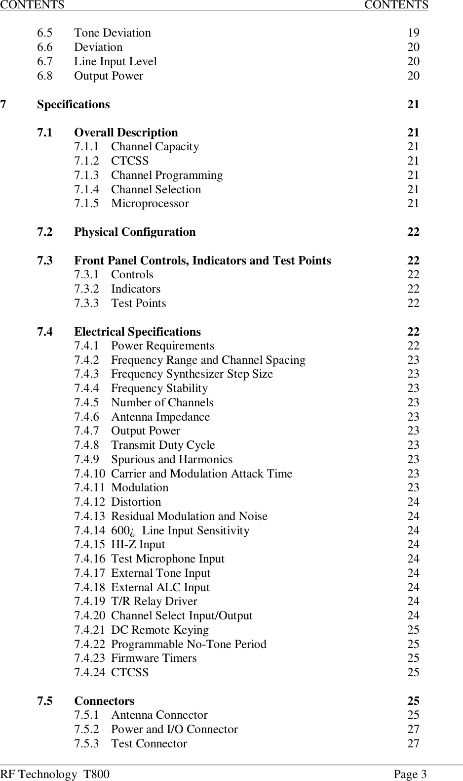
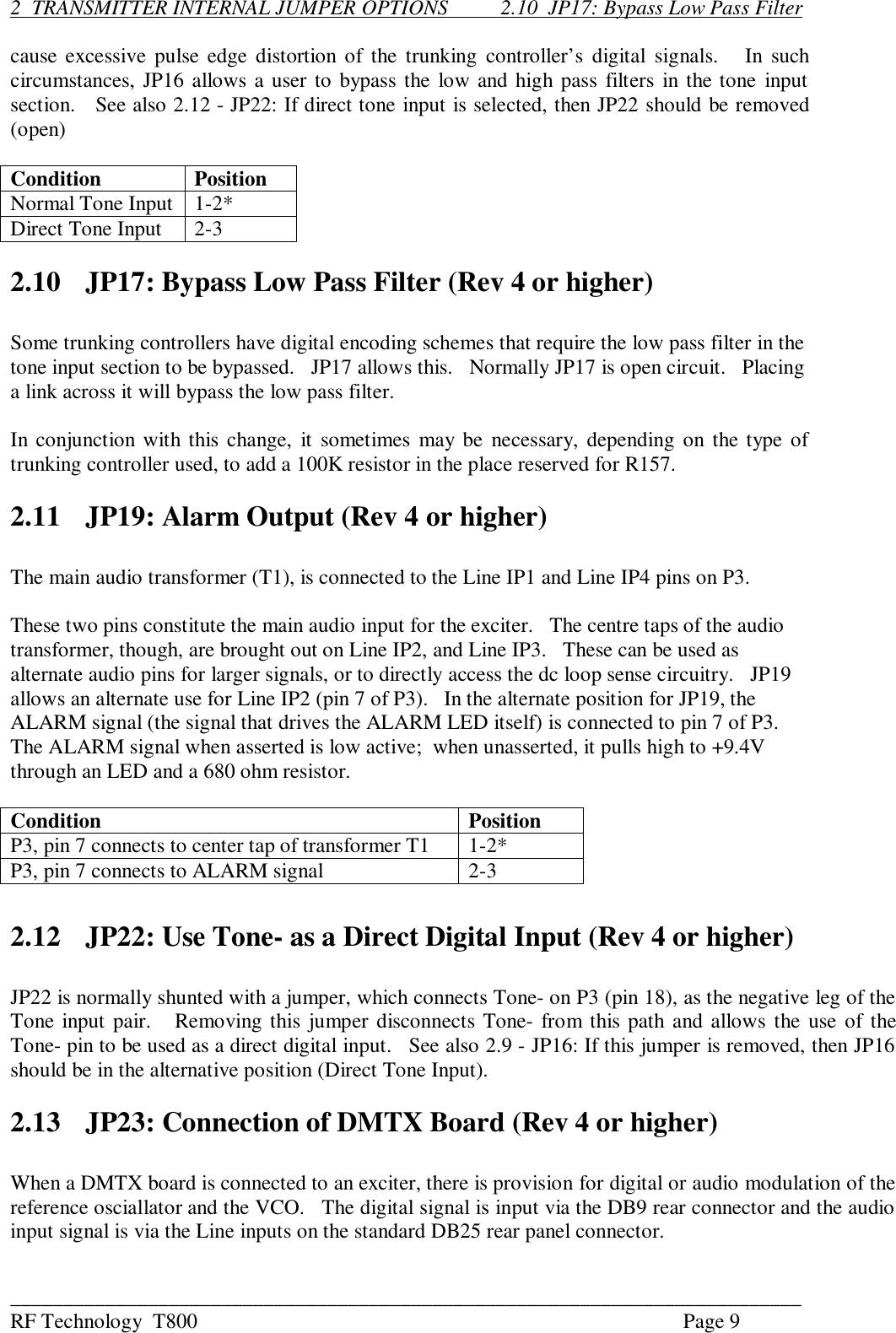
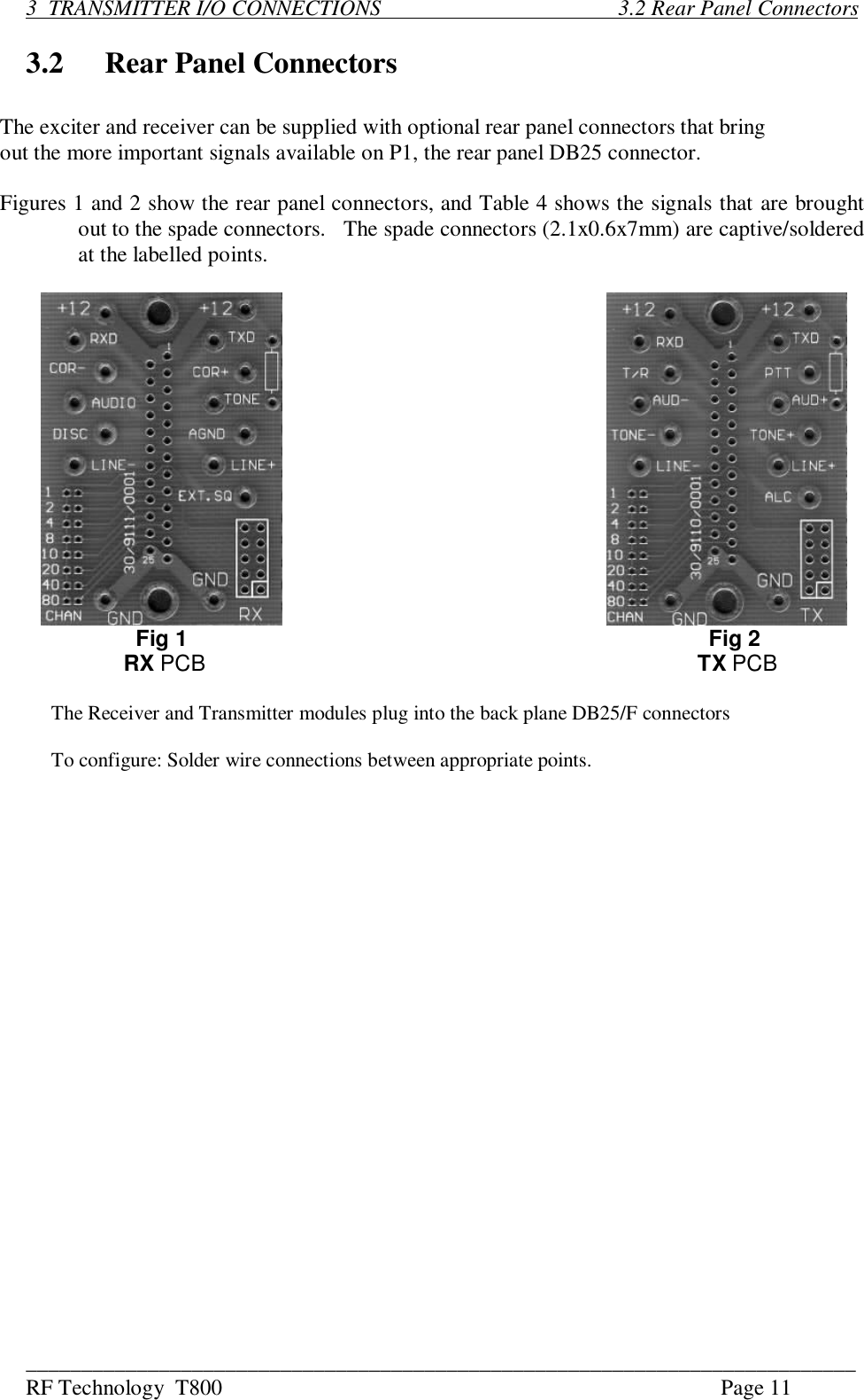
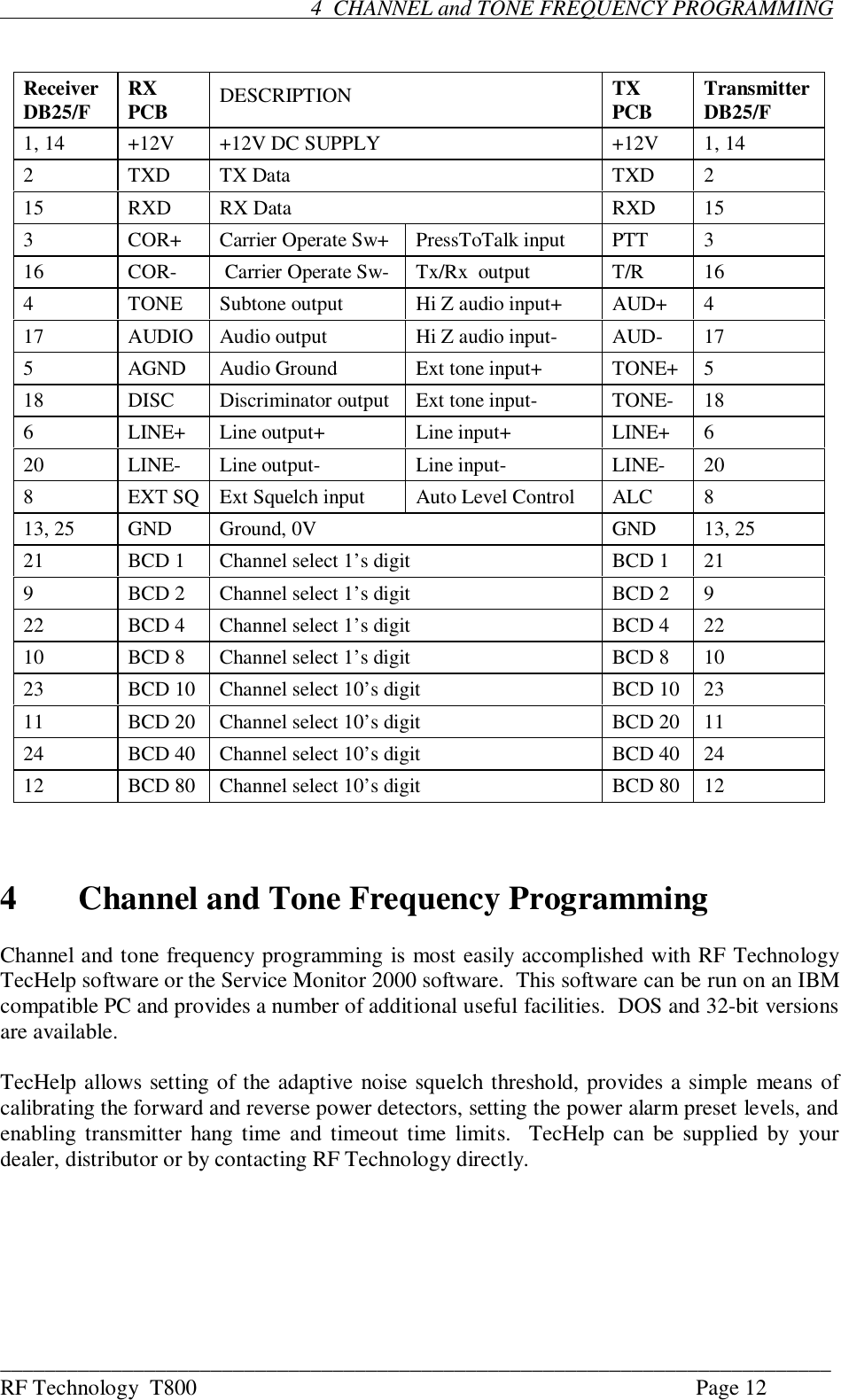
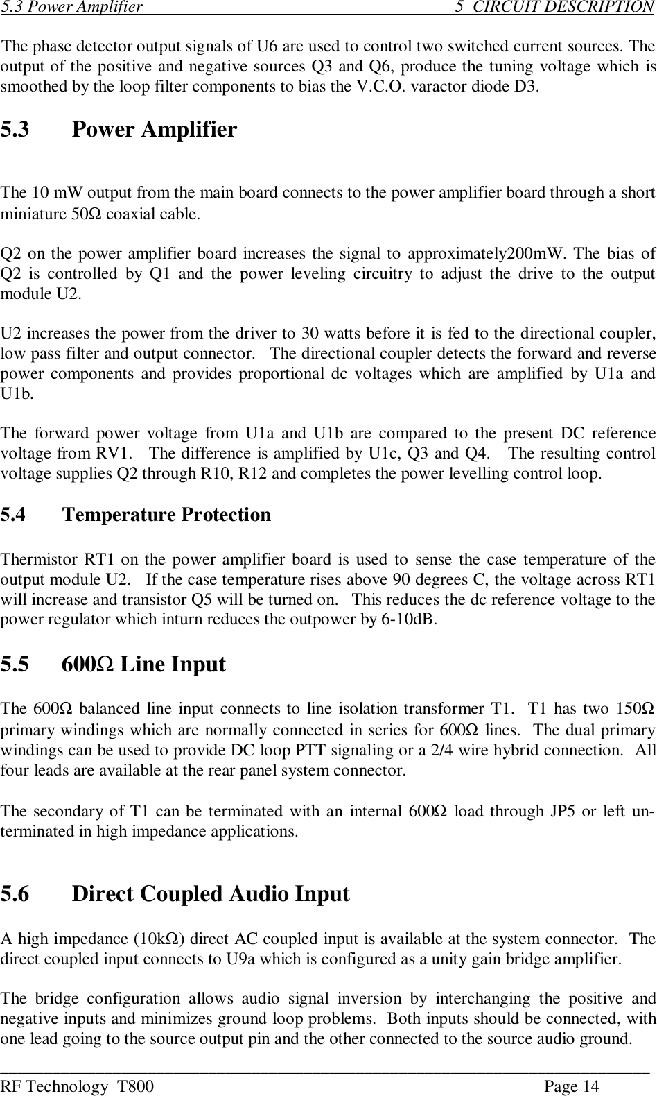
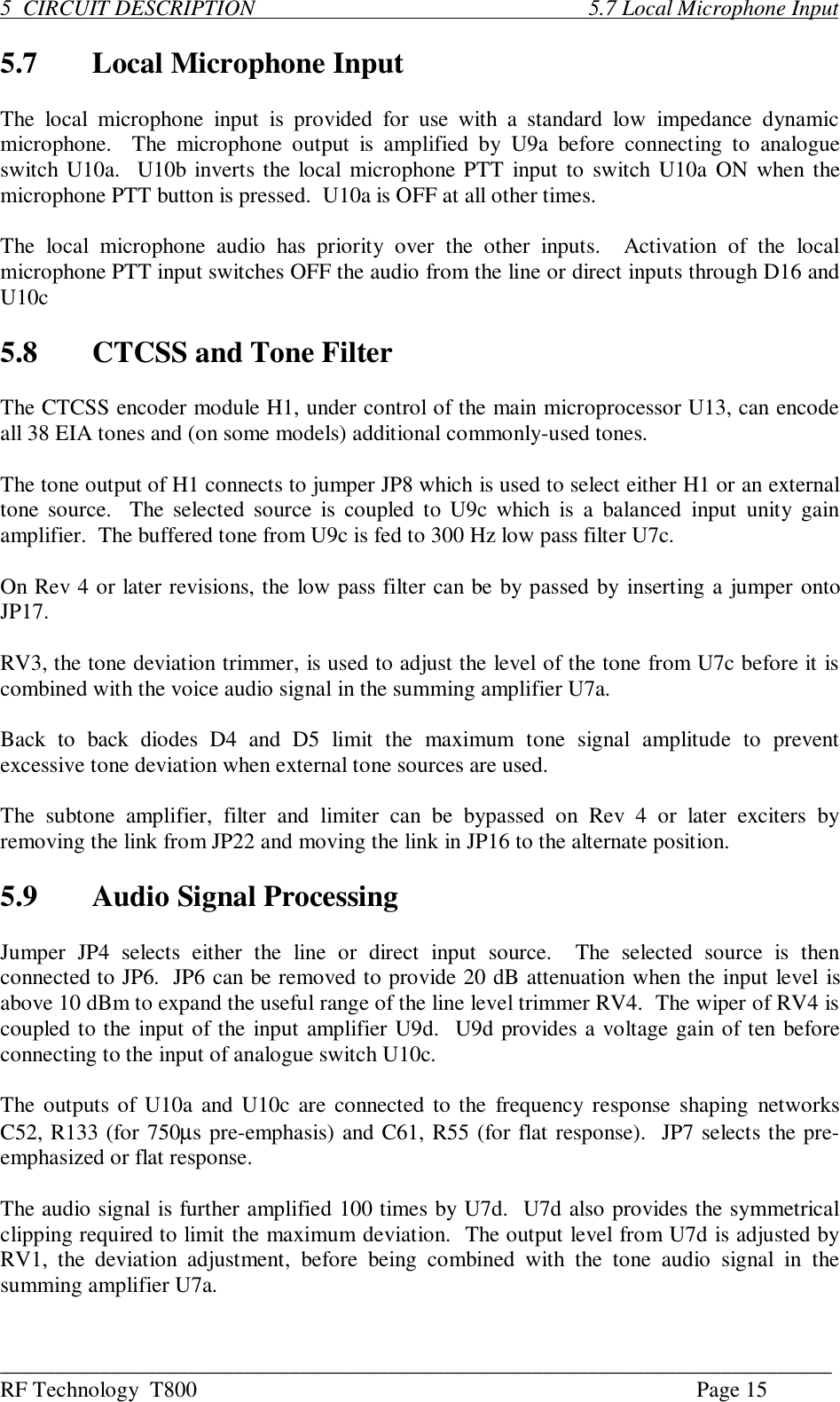
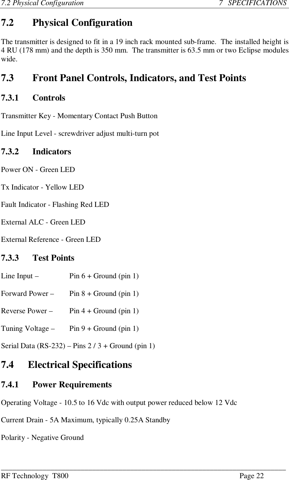
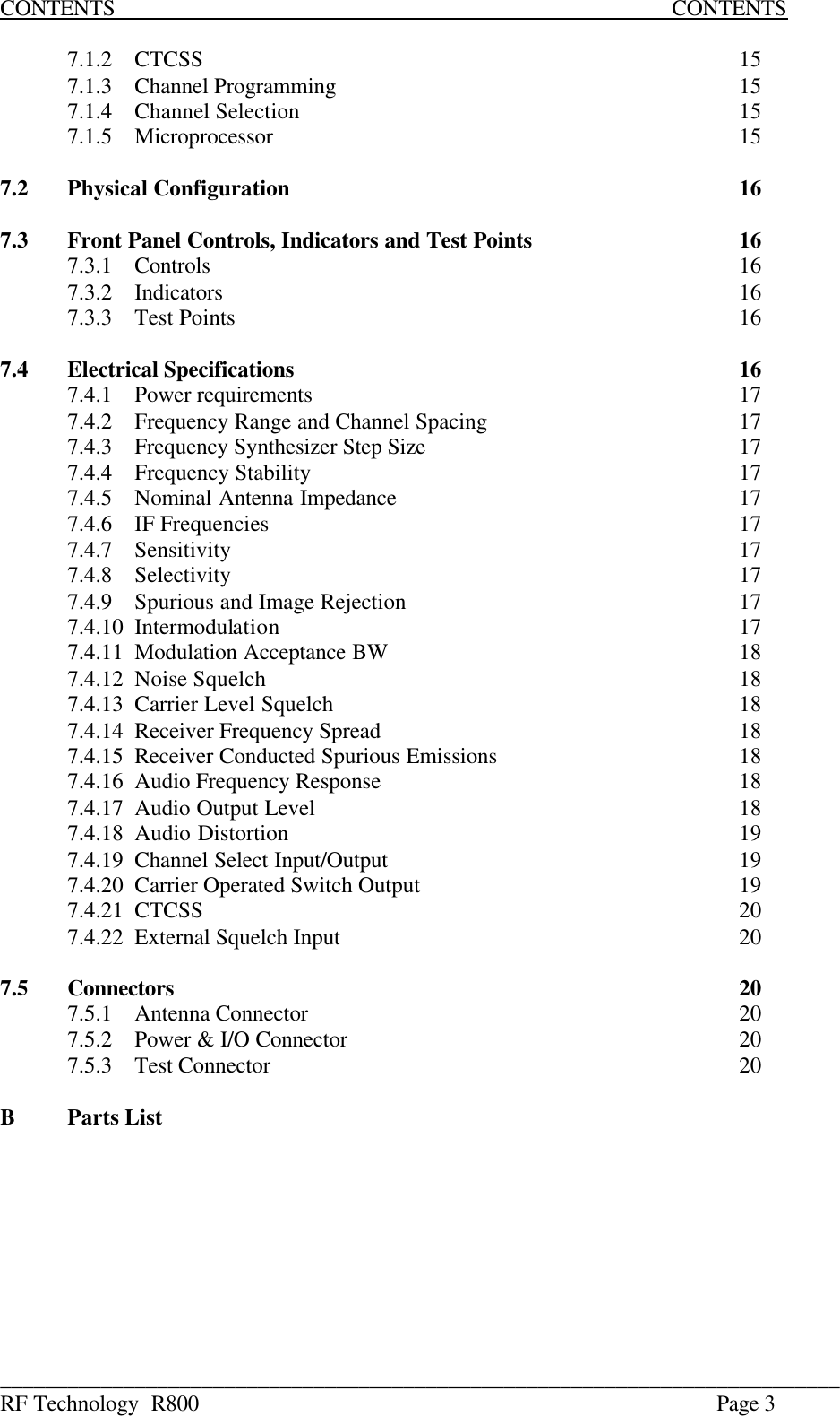
![___________________________________________________________________________RF Technology T800 Page 103.1 25 Pin Connector 3 TRANSMITTER I/O CONNECTIONSCondition PositionNo DMTX board 1-2, 5-6*DMTX board connected 2-3, 4-5In addition to the jumper changes, a wire link or zero ohm resistor must be connected in theplace marked for R159.3Transmitter I/O Connections3.1 25 Pin ConnectorThe D-shell 25 pin connector is the main interface to the transmitter. The pin connections aredescribed in table 3.Function Signal Pins SpecificationDC power +12 Vdc 0 Vdc 1, 1413, 25 +11.4 to 16 Vdc GroundChannel Select 124810204080219221023112412BCD Coded0 = Open Circuitor 0 Vdc1 = +5 to +16 VdcRS232 Data InOut 152Test and Programming use9600, 8 data 2 stop bits600Ω Line HighLow 206Transformer IsolatedBalanced 0dBm Output150Ω / Hybrid 719Direct PTT input 3Ground to key PTTT/R Relay driver output 16 Open collector,250mA/30VSub-Audible Tone Input [+] 5>10kΩ, AC coupled[-] 18 (1-250Hz)High-Z Audio Input [+] 4>10kΩ, AC coupled[-] 17 (10Hz-3kHz)External ALC input 8 <0.5V/1mA to obtain>30dB attenuation, O/Cfor maximum powerTable 3: Pin connections and explanations for the main 25-pin, D connector.](https://usermanual.wiki/RF-Technology/1UTR800CN/User-Guide-1512886-Page-10.png)