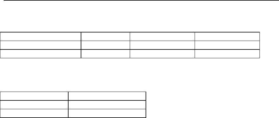
RF Technology 1UTR800CN UHF BASE STATION User Manual R800 Manual
RF Technology Pty Ltd UHF BASE STATION R800 Manual
Users Manual

Eclipse Series
RF Technology
rfinfo@rftechnology.com.au
September 2003 Revision 2
T800 Transmitter
Operation and Maintainance Manual
This manual is produced by RF Technology Pty Ltd
10/8 Leighton Place, Hornsby NSW 2077 Australia
Copyright © 1997, 1998, 2003 RF Technology

___________________________________________________________________________
RF Technology T800 Page 2
CONTENTS CONTENTS
1. Operating Instructions 5
1.1 Front Panel controls and Indicators 5
1.1.1 PTT 5
1.1.2 Line 5
1.1.3 PWR LED 5
1.1.4 TX LED 5
1.1.5 ALARM LED 6
1.1.6 ALC LED 6
1.1.7 REF LED 6
1.1.8 TEST MIC 6
2. Transmitter Internal Jumper Options 7
2.1 JP2: EPROM Type 7
2.2 JP3: Dc Loop PTT 7
2.3 JP4: Audio Input source 7
2.4 JP5: 600 ¿ Termination 7
2.5 JP6: Input Level Attenuation8
2.6 JP7: Audio Frequency Response 8
2.7 JP8:
Subaudible Tone Source
8
2.8 JP9, JP10, JP11 dc Loop PTT Input Configuration JP3 (1-2) 8
2.9 JP16: Direct Digital Input (Rev 4 or Higher) 8
2.10 JP17:
Bypass Low Pass Filter (Rev 4 or Higher)
9
2.11 JP19: Alarm Output (Rev 4 or Higher) 9
2.12 JP22: Use Tone- as a Direct Digital Input (Rev 4 or Higher) 9
2.13 JP23: Connection of DMTX Board (Rev 4 or Higher) 9
3. Transmitter Internal Jumper Options
3.1 25 Pin Connector 10
3.2 Rear Panel Connectors 11
4. Channel and Tone Frequency Programming 12
5. Circuit Description 13
5.1 VCO Section 13
5.2 PLL Section 13
5.3 Power Amplifier 14
5.4 Temperature Protection 14
5.5 600 ¿ Line Input 14
5.6 Direct coupled Audio Input 14
5.7 Local Microphone Input 15
5.8 CTCSS and Tone Filter 15
5.9 Audio Signal Processing 15
5.10 PTT and DC Remote Control 16
5.11 Microprocessor Controller 16
5.12 Voltage Regulator 17
6. Field Alignment Procedure 17
6.1 Standard Test Conditions 18
6.2
VCO Alignment
18
6.3 TCXO Calibration 18
6.4 Modulation Balance 19

___________________________________________________________________________
RF Technology T800 Page 3
CONTENTS CONTENTS
6.5 Tone Deviation 19
6.6 Deviation 20
6.7 Line Input Level 20
6.8 Output Power 20
7Specifications 21
7.1 Overall Description 21
7.1.1 Channel Capacity 21
7.1.2 CTCSS 21
7.1.3 Channel Programming 21
7.1.4 Channel Selection 21
7.1.5 Microprocessor 21
7.2 Physical Configuration 22
7.3 Front Panel Controls, Indicators and Test Points 22
7.3.1 Controls 22
7.3.2 Indicators 22
7.3.3 Test Points 22
7.4 Electrical Specifications 22
7.4.1 Power Requirements 22
7.4.2 Frequency Range and Channel Spacing 23
7.4.3 Frequency Synthesizer Step Size 23
7.4.4 Frequency Stability 23
7.4.5 Number of Channels 23
7.4.6 Antenna Impedance 23
7.4.7 Output Power 23
7.4.8
Transmit Duty Cycle
23
7.4.9 Spurious and Harmonics 23
7.4.10 Carrier and Modulation Attack Time 23
7.4.11 Modulation 23
7.4.12 Distortion 24
7.4.13 Residual Modulation and Noise 24
7.4.14
600¿ Line Input Sensitivity
24
7.4.15 HI-Z Input 24
7.4.16 Test Microphone Input 24
7.4.17 External Tone Input 24
7.4.18 External ALC Input 24
7.4.19 T/R Relay Driver 24
7.4.20 Channel Select Input/Output 24
7.4.21 DC Remote Keying 25
7.4.22 Programmable No-Tone Period 25
7.4.23 Firmware Timers 25
7.4.24 CTCSS 25
7.5 Connectors 25
7.5.1 Antenna Connector 25
7.5.2 Power and I/O Connector 27
7.5.3 Test Connector 27

___________________________________________________________________________
RF Technology T800 Page 4
CONTENTS CONTENTS
AEngineering Diagrams
A1 Block Diagram
A2 Circuit Diagram
A3 Component Overlay Diagram
BParts List

___________________________________________________________________________
RF Technology T800 Page 5
1 OPERATING INSTRUCTIONS
WARNING
Changes or modifications not expressly approved by
RF Technology could void your authority to operate this
equipment. Specifications may vary from those given in
this document in accordance with requirements of local
authorities. RF Technology equipment is subject to
continual improvement and RF Technology reserves the
right to change performance and specification without
further notice.
1Operating Instructions
1.1 Front Panel Controls and Indicators
1.1.1 PTT
A front-panel push-to-talk (PTT) button is provided to facilitate bench and field tests and
adjustments. The button is a momentary action type. When keyed, audio from the line input
is disabled so that a carrier with sub-tone is transmitted. The front-panel microphone input is
not enabled in this mode, but it is enabled when the PTT line on that socket is pulled to
ground.
1.1.2 Line
The LINE trimpot is accessible by means of a small screwdriver from the front panel of the
module. It is used to set the correct sensitivity of the line and direct audio inputs. It is
factory preset to give 60% of rated deviation with an input of 0dBm (1mW on 600
Ω
equivalent to 775mV RMS or about 2.2V peak-to-peak) at 1kHz. The nominal 60% deviation
level may be adjusted by measuring between pins 6 and 1 on the test socket, and adjusting the
pot. By this means an input sensitivity from approximately -30dBm to +10dBm may be
established.
An internal jumper provides a coarse adjustment step of 20dB. Between the jumper and the
trimpot, a wide range of input levels may be accommodated.
1.1.3 POWER LED
The PWR LED shows that the dc supply is connected to the receiver.
1.1.4 TX LED
The TX LED illuminates when the transmitter is keyed. It will not illuminate (and an Alarm
cadence will be shown) if the synthesizer becomes unlocked, or the output amplifier supply is
interrupted by the microprocessor.
___________________________________________________________________________
RF Technology T800 Page 6
1.1.5 Alarm LED 1 OPERATING INSTRUCTIONS
1.1.5 ALARM LED
The Alarm LED can indicate several fault conditions if they are detected by the self test
program. The alarm indicator shows the highest priority fault present. Receivers using
software issue 5 and higher use the cadence of the LED flash sequence to indicate the alarm
condition. Refer to table 1. Receivers using software issue 4 and lower use the LED flash
rate to indicate the alarm condition. Refer to table 2.
LED Flash Cadence Fault Condition
5 flashes, pause Synthesizer unlocked
4 flashes, pause Tuning voltage out of range
3 flashes, pause Low forward power
2 flashes, pause High reverse (reflected) power
1 flash, pause Low dc supply voltage
LED ON continuously
Transmitter timed out
Table 1: Interpretations of LED flash cadence
Indication Fault Condition
Flashing, 8 per second Synthesizer unlocked
Flashing, 4 per second Tuning voltage outside correct range
Flashing, 2 per second Low forward power
Flashing, 1 per second High reverse power
Continuous dc supply voltage low or high
Table 2: Interpretations of LED flash speed, for early models
1.1.6 ALC LED
The ALC LED indicates that
the transmitter output power is being controlled by an external
amplifier through the external ALC input.
1.1.7 REF LED
The REF LED indicates that the synthesizer frequency reference is locked to an external
reference.
1.1.8 TEST MIC.
The TEST MIC. DIN socket is provided for use with a standard mobile or handset 200 Ohm
dynamic microphone. The external audio inputs are disabled when the TEST MIC’S PTT is
on.
___________________________________________________________________________
RF Technology T800 Page 7
2TRANSMITTER INTERNAL JUMPER OPTIONS
2Transmitter Internal Jumper Options
In the following subsections
an asterisk (*) signifies the standard (Ex-Factory) configuration
of a jumper.
2.1 JP2: EPROM Type
Condition Position
27C256 2-3 *
27C64 1-2
2.2 JP3: 600 Ohm Line Dc Loop PTT Input
By default, Eclipse exciters can be keyed up by pulling the PTT signal low, or by dc loop
signalling on the audio pair.
This jumper enables or disables this second method.
Condition Position
dc loop connected (enabled) 1-2 *
dc loop not connected (bypassed) 2-3
2.3 JP4: Audio Input Source Selection
Either the 600Ω or the high-Z balanced inputs may be selected.
Condition Position
600Ω Input 2-3 *
High-impedance Input 1-2
2.4 JP5: 600 ¿ Termination
Normally the Line Input is terminated in 600 ¿ . The 600 ohm termination can be removed
by choosing the alternate position.
Condition Position
600¿ Termination 1-2*
No Termination 2-3
___________________________________________________________________________
RF Technology T800 Page 8
2.5 JP6: Input Level Attenuation 2 TRANSMITTER JUMPER OPTIONS
2.5 JP6: Input Level Attenuation
This jumper permits coarse input sensitivity to be set. In the default position, the unit expects
a line level of 0dBm (nominal) at its Line Input. In the alternate position, levels of
+20dBm(nominal) can be accepted.
Condition Position
0dB attenuation 1-2 *
20dB attenuation 2-3
2.6 JP7: Audio Frequency Response
Condition Position
750 uSec. Pre-emphasis 1-2 *
Flat Response 2-3
2.7 JP8: Sub-audible Tone Source
Condition Position
Internal CTCSS 1-2, 4-5 *
External input 2-3, 5-6
2.8 JP9/10/11: dc Loop Configuration
Dc loop current on the audio pair is normally sourced externally. The Eclipse exciters loop
the current through an opto-isolator. When the current flows the exciter keys up.
An alternative arrangement is possible. The exciters can source the current and an external
device can provide the dc loop.
These three jumpers select the appropriate mode.
Condition JP9 JP10 JP11
Current Loop Input ON OFF OFF *
12Vdc Loop source OFF ON ON
2.9 JP16: Direct Digital Input (Rev 4 or Higher)
Some trunking controllers have digital encoding schemes which operate to very low
frequencies. The elliptical filter, used as a 250Hz low pass filter in the tone section, can
___________________________________________________________________________
RF Technology T800 Page 9
2 TRANSMITTER INTERNAL JUMPER OPTIONS 2.10 JP17: Bypass Low Pass Filter
cause excessive pulse edge distortion of the trunking controller’s digital signals. In such
circumstances, JP16 allows a user to bypass the low and high pass filters in the
tone input
section. See also 2.12 - JP22: If direct tone input is selected, then JP22 should be removed
(open)
Condition Position
Normal Tone Input 1-2*
Direct Tone Input 2-3
2.10 JP17: Bypass Low Pass Filter (Rev 4 or higher)
Some trunking controllers have digital encoding schemes that require the low pass filter in the
tone input section to be bypassed. JP17 allows this. Normally JP17 is open circuit. Placing
a link across it will bypass the low pass filter.
In conjunction with this change, it sometimes may be necessary, depending on the type of
trunking controller used, to add a 100K resistor in the place reserved for R157.
2.11 JP19: Alarm Output (Rev 4 or higher)
The main audio transformer (T1), is connected to the Line IP1 and Line IP4 pins on P3.
These two pins constitute the main audio input for the exciter. The centre taps of the audio
transformer, though, are brought out on Line IP2, and Line IP3. These can be used as
alternate audio pins for larger signals, or to directly access the dc loop sense circuitry. JP19
allows an alternate use for Line IP2 (pin 7 of P3). In the alternate position for JP19, the
ALARM signal (the signal that drives the ALARM LED itself) is connected to pin 7 of P3.
The ALARM signal when asserted is low active; when unasserted, it pulls high to +9.4V
through an LED and a 680 ohm resistor.
Condition Position
P3, pin 7 connects to center tap of transformer T1 1-2*
P3, pin 7 connects to ALARM signal 2-3
2.12 JP22: Use Tone- as a Direct Digital Input (Rev 4 or higher)
JP22 is normally shunted with a jumper, which connects Tone- on P3 (pin 18), as the negative leg of the
Tone input pair. Removing this jumper disconnects Tone- from this path and allows the use of the
Tone- pin to be used as a direct digital input. See also 2.9 - JP16: If this jumper is removed, then JP16
should be in the alternative position (Direct Tone Input).
2.13 JP23: Connection of DMTX Board (Rev 4 or higher)
When a DMTX board is connected to an exciter, there is provision for digital or audio modulation of the
reference osciallator and the VCO. The digital signal is input via the DB9 rear connector and the audio
input signal is via the Line inputs on the standard DB25 rear panel connector.
___________________________________________________________________________
RF Technology T800 Page 10
3.1 25 Pin Connector 3 TRANSMITTER I/O CONNECTIONS
Condition Position
No DMTX board 1-2, 5-6*
DMTX board connected 2-3, 4-5
In addition to the jumper changes, a wire link or zero ohm
resistor must be connected in the
place marked for R159.
3Transmitter I/O Connections
3.1 25 Pin Connector
The D-shell
25 pin connector is the main interface to the transmitter. The pin connections are
described in table 3.
Function Signal Pins Specification
DC power +12 Vdc
0 Vdc 1, 14
13, 25 +11.4 to 16 Vdc
Ground
Channel Select 1
2
4
8
10
20
40
80
21
9
22
10
23
11
24
12
BCD Coded
0 = Open Circuit
or 0 Vdc
1 = +5 to +16 Vdc
RS232 Data In
Out 15
2
Test and Programming use
9600, 8 data 2 stop bits
600Ω Line High
Low 20
6Transformer Isolated
Balanced 0dBm Output
150Ω / Hybrid 7
19
Direct PTT input 3Ground to key PTT
T/R Relay driver output 16 Open collector,250mA/30V
Sub-Audible Tone Input [+] 5>10kΩ, AC coupled
[-] 18 (1-250Hz)
High-Z Audio Input [+] 4>10kΩ, AC coupled
[-] 17 (10Hz-3kHz)
External ALC input 8 <0.5V/1mA to obtain
>30dB attenuation, O/C
for maximum power
Table 3: Pin connections and explanations for the main 25-pin, D connector.
___________________________________________________________________________
RF Technology T800 Page 11
3 TRANSMITTER I/O CONNECTIONS 3.2 Rear Panel Connectors
3.2 Rear Panel Connectors
The exciter and receiver can be supplied with optional rear panel connectors that bring
out the more important signals available on P1, the rear panel DB25 connector.
Figures 1 and 2 show the rear panel connectors, and Table 4 shows the signals that are brought
out to the spade connectors. The spade connectors (2.1x0.6x7mm) are captive/soldered
at the labelled points.
Fig 1 Fig 2
RX PCB TX PCB
The Receiver and Transmitter modules plug into the back plane DB25/F connectors
To configure: Solder wire connections between appropriate points.

___________________________________________________________________________
RF Technology T800 Page 12
4 CHANNEL and TONE FREQUENCY PROGRAMMING
Receiver
DB25/F RX
PCB DESCRIPTION TX
PCB Transmitter
DB25/F
1, 14 +12V +12V DC SUPPLY +12V 1, 14
2TXD TX Data TXD 2
15 RXD RX Data RXD 15
3COR+ Carrier Operate Sw+ PressToTalk input PTT 3
16 COR- Carrier Operate Sw- Tx/Rx output T/R 16
4TONE Subtone output Hi Z audio input+ AUD+ 4
17 AUDIO Audio output Hi Z audio input- AUD- 17
5AGND Audio Ground Ext tone input+ TONE+ 5
18 DISC Discriminator output Ext tone input- TONE- 18
6LINE+ Line output+ Line input+ LINE+ 6
20 LINE- Line output- Line input- LINE- 20
8EXT SQ Ext Squelch input Auto Level Control ALC 8
13, 25 GND Ground, 0V GND 13, 25
21 BCD 1 Channel select 1’s digit BCD 1 21
9BCD 2 Channel select 1’s digit BCD 2 9
22 BCD 4 Channel select 1’s digit BCD 4 22
10 BCD 8 Channel select 1’s digit BCD 8 10
23 BCD 10 Channel select 10’s digit BCD 10 23
11 BCD 20 Channel select 10’s digit BCD 20 11
24 BCD 40 Channel select 10’s digit BCD 40 24
12 BCD 80 Channel select 10’s digit BCD 80 12
4
Channel and Tone Frequency Programming
Channel and tone frequency programming is most easily accomplished with RF Technology
TecHelp software or the Service Monitor 2000 software. This software can be run on an IBM
compatible PC and provides a number of additional useful facilities. DOS and 32-bit versions
are available.
TecHelp allows setting of the adaptive noise squelch threshold, provides a simple means of
calibrating the forward and reverse power detectors, setting the power alarm preset levels, and
enabling transmitter hang time and timeout time limits. TecHelp can be supplied by your
dealer, distributor or by contacting RF Technology directly.

___________________________________________________________________________
RF Technology T800 Page 13
5 CIRCUIT DESCRIPTION 5.1 VCO Section
5Circuit Description
The following descriptions should be read as an aid to understanding the block and schematic
diagrams given in the appendix of this manual.
5.1 VCO Section
The Voltage Controlled Oscillator uses a bipolar junction FET Q19
which oscillates at the
required transmitter output frequency. Varactor diodes D25 and D26 are used by the PLL
circuit to keep the oscillator on the desired frequency. A second varactor diode D3 is used to
frequency
modulate the VCO. Transistor Q20 is used as an active filter to reduce the noise
on the oscillator supply voltage.
The VCO is keyed ON by the microcontroller through Q10. It is keyed ON when any of the
PTT inputs are active and OFF at all other times.
The VCO output is amplified and buffered by monolithic amplifiers MA2 and MA3 before
being fed to the PLL IC U6.
Amplifiers MA1, MA4 and MA5 increase the VCO output to approximately 10 mW to drive
the power amplifier. MA1 is not switched on until the PLL has locked and had time to settle.
This prevents any momentary off channel transmission when the transmitter is keyed.
5.2 PLL Section
The frequency reference for the synthesiser is a crystal oscillator using transistors Q26 and
Q27 and crystal Y3. The temperature stability is better than 5 ppm and it can be synchronised
to an external reference for improved stability. External reference option board 11/9119 is
required when using an external reference.
A positive temperature coefficient thermistor, XH1, is used in versions intended for operation
down to -30 degrees Celsius. The thermistor heats the crystal's case to maintain its
temperature above -10 degrees thus extending the oscillator stability of 5 ppm down to -30
degrees ambient.
Varactor diodes D27-30
are used to frequency modulate the oscillator. The processed transmit
audio signal from U7b varies the diodes bias voltage to modulate the reference frequency.
This extends the modulation capability down to a few Hz for sub-audible tones and digital
squelch codes. A
two point modulation scheme is used with the audio also being fed to the
VCO to modulate the higher audio frequencies.
The 12.8 MHz output of Q27 is amplified by Q28 and Q29 to drive the reference input of the
PLL synthesiser IC U6. This IC is a single chip synthesiser which includes a 1.1 GHz pre-
scaler, programmable divider, reference divider and phase/frequency detector. The frequency
data for U6 is supplied via a serial data link by the microcontroller.

___________________________________________________________________________
RF Technology T800 Page 14
5.3 Power Amplifier 5 CIRCUIT DESCRIPTION
The phase detector output signals of U6 are used to control two switched current sources. The
output of the positive and negative sources Q3 and Q6, produce the tuning voltage which is
smoothed by the loop filter components to bias the V.C.O. varactor diode D3.
5.3 Power Amplifier
The 10 mW output from the main board connects to the power amplifier board through a short
miniature 50Ω coaxial cable.
Q2 on the power amplifier board increases the signal to approximately200mW.
The bias of
Q2 is controlled by Q1 and the power leveling circuitry to adjust the drive to the output
module U2.
U2 increases the power from the driver to 30 watts before it is fed to the directional coupler,
low pass filter and output connector. The directional coupler detects the forward and reverse
power components and provides proportional dc voltages which are amplified by U1a and
U1b.
The forward power voltage from U1a and U1b are compared to the present DC reference
voltage from RV1.
The difference is amplified by U1c, Q3 and Q4. The resulting control
voltage supplies Q2 through R10, R12 and completes the power levelling control loop.
5.4 Temperature Protection
Thermistor RT1 on the power amplifier board is used to sense the case temperature of the
output module U2. If the case temperature rises above 90 degrees C, the voltage across RT1
will increase and transistor Q5 will be turned on. This reduces the dc reference voltage to the
power regulator which inturn reduces the outpower by 6-10dB.
5.5 600Ω Line Input
The 600Ω balanced line input connects to line isolation transformer T1. T1 has two 150Ω
primary windings which are normally connected in series for 600Ω
lines. The dual primary
windings can be used to provide DC loop PTT signaling or a 2/4 wire hybrid connection. All
four leads are available at the rear panel system connector.
The secondary of T1 can be terminated with an internal 600Ω
load through JP5 or left un-
terminated in high impedance applications.
5.6 Direct Coupled Audio Input
A high impedance (10k
Ω) direct AC coupled input is available at the system connector. The
direct coupled input connects to U9a which is configured as a unity gain bridge amplifier.
The bridge configuration allows audio signal inversion by interchanging the positive and
negative inputs and minimizes ground loop problems. Both inputs should be connected, with
one lead going to the source output pin and the other connected to the source audio ground.

___________________________________________________________________________
RF Technology T800 Page 15
5 CIRCUIT DESCRIPTION 5.7 Local Microphone Input
5.7 Local Microphone Input
The local microphone input is provided for use with a
standard low impedance dynamic
microphone. The microphone output is amplified by U9a before connecting to analogue
switch U10a. U10b inverts the local microphone PTT input to switch U10a ON when the
microphone PTT button is pressed. U10a is OFF at all other times.
The local microphone audio has priority over the other inputs. Activation of the local
microphone PTT input switches OFF the audio from the line or direct inputs through D16 and
U10c
5.8 CTCSS and Tone Filter
The CTCSS encoder module H1, under control of the main microprocessor U13, can encode
all 38 EIA tones and (on some models) additional commonly-used tones.
The tone output of H1 connects to jumper JP8
which is used to select either H1 or an external
tone source. The selected source is coupled to U9c which is a balanced input unity gain
amplifier. The buffered tone from U9c is fed to 300 Hz low pass filter U7c.
On Rev 4 or later revisions, the low pass filter can be by passed by inserting a jumper onto
JP17.
RV3, the tone deviation trimmer, is used to adjust the level of the tone from U7c before it is
combined with the voice audio signal in the summing amplifier U7a.
Back to back diodes D4 and D5 limit the maximum tone signal amplitude to prevent
excessive tone deviation when external tone sources are used.
The subtone amplifier, filter and limiter can be bypassed on Rev 4 or later exciters by
removing the link from JP22 and moving the link in JP16 to the alternate position.
5.9 Audio Signal Processing
Jumper JP4 selects either the line or direct input source. The selected source is then
connected to JP6. JP6 can be removed to provide 20 dB attenuation when the input level is
above 10 dBm to expand the useful range of the line level trimmer RV4. The wiper of RV4 is
coupled to the input of the input amplifier U9d. U9d provides a voltage gain of ten before
connecting to the input of analogue switch U10c.
The outputs of U10a and U10c are connected to the frequency response shaping networks
C52, R133 (for 750
µs pre-emphasis) and C61, R55 (for flat response). JP7 selects the pre-
emphasized or flat response.
The audio signal is further amplified 100 times by U7d. U7d also provides the symmetrical
clipping required
to limit the maximum deviation. The output level from U7d is adjusted by
RV1, the deviation adjustment, before being combined with the tone audio signal in the
summing amplifier U7a.

___________________________________________________________________________
RF Technology T800 Page 16
5.10 PTT and DC Remote Control 5 CIRCUIT DESCRIPTION
The composite audio from U7a is fed through the 3Khz low pass filter U7b. When the links
on JP23 are in their default state, the filtered audio is coupled to the TCXO voltage tuning
input and the modulation balance trimmer RV2. RV2, R99 and R98 attenuate the modulation
signal before applying it to the VCO via varactor D3.
When DMTX board option is required, Jumper JP23 allows the audio paths to be re-routed.
The DMTX board provides for an external digital modulation input signal.
When the two
links on JP23 are positioned in the middle of the 6 pin header, the audio from the exciter is
passed to the DMTX board via pin 5 of JP15, where the signal is conditioned and then
returned from the DMTX board via pin 2 of JP15, and passed to the two modulation points.
RV2 adjusts level of the audio used to modulate the VCO. This primarily effects the deviation
of audio frequencies above 500 Hz. RV2 is used to balance the high and low frequency
deviation to obtain a flat frequency response relative to the desired characteristic.
5.10 PTT and DC Remote Control
Two main PTT inputs are provided. The first, a direct logic level input, is connected to pin 3
of the system connector. The transmitter can be keyed by applying
a logic low or ground on
pin 3. Pin 3 connects to the PTT logic and microprocessor through D10.
DC current loop control can be used for remote PTT operation.
The current loop can be
configured by JP9, JP10 and JP11 for use with either a remote free switch or a remote
switched source.
Opto-isolator ISO1 is used to isolate the loop current signal from the transmitter PTT logic.
The loop current passes through the input of ISO1 and the output of ISO1 connects to the PTT
logic.
A bridge consisting of diodes D6, D8, D9 and D14 ensures correct operation regardless of the
current polarity. Q17 limits the current and D7 limits the voltage input of ISO1. Any low
voltage current source capable of providing 2mA at 4V or switching circuit with less than
4.8k¿ loop resistance can be used to switch the DC loop.
The test PTT button on the front panel and the local microphone PTT button will also key the
transmitter. Both of these also mute the line audio input. The microphone line also enables
that audio input.
A DMTX board can also cause the exciter to key up. When TX (or TTL_TX) signal is
received by the DMTX board, it pulls pin 6 of JP15 low, which in turn asserts the
PTT_WIRE-OR signal, causing the microprocessor (U13) to key the exciter up.
5.11 Microprocessor Controller
The microprocessor controller circuit uses a single-chip eight bit processor and several
support chips. The processor U13 includes non-volatile EE memory for channel frequencies,
tones, and other information. It also has an asynchronous serial port, a synchronous serial
port and an eight bit analogue to digital converter.

___________________________________________________________________________
RF Technology T800 Page 17
5 CIRCUIT DESCRIPTION 5.12 Voltage Regulator
The program is stored in U5, a CMOS EPROM. U4 is an address latch for the low order
address bits. U2 is used to read the channel select lines onto the data bus. U11 is an address
decoder for U5 and U2. U3 is a supervisory chip which keeps the processor reset unless the
+5 Volt supply is within operating limits. U1 translates the asynchronous serial port data to
standard RS232 levels.
The analogue to digital converter is used to measure the forward and reverse power, tuning
voltage and dc supply voltage.
If the processor detects that the PTT_WIRE_OR signal is asserted low, it will
attempts to key
the exciter up. If will first attempt to key the VCO through Q10, and if the LD pin goes high,
it will switch the 9.2 Volt transmit line through Q14 and Q16.
asserting Q16 has the effect of
also asserting the yellow Tx LED (D12) on the front panel, enabling the local 25W power
amplifier, and causing the T/R Relay output to be pulled low. D24 is
30 volt zener which
protects Q25 from both excessive voltages or reverse voltages.
Should there be a problem with either the tuning volts, or the battery voltage, the VCO
locking, the forward power, or the reverse power, the microprocessor will assert the ALARM
LED, through Q1. Depending on the setting of Jumper JP19, the ALARM signal can be
brought out on pin 7 of P3.
5.12 Voltage Regulator
The
dc input voltage is regulated down to 9.4 Vdc by a discrete regulator circuit. The series
pass transistor Q23 is driven by error amplifiers Q8 and Q18. Q9 is used to start up the
regulator and once the circuit turns on, it plays no further part in the operation.
The +5 Volt supply for the logic circuits is provided by an integrated circuit regulator U14
which is run from the regulated 9.4 Volt supply.
Jumper JP18 is not normally fitted to the board, and is bridged with a 12mil track on the
component side of the board. It is provided so that the 9.4V load can be isolated from the
supply by the service department to aid in fault finding.
Jumpers JP20 and JP21 are also not normally fitted on the board, and are usually bridged with
a 12mil track on the component side. They allow U14 to be isolated from its input, or its
output or both.
6Field Alignment Procedure
The procedures given below may be used to align the transmitter in the field. Normally,
alignment is only required when changing operating frequencies, or after component
replacement.
The procedures below do not constitute an exhaustive test or a complete alignment of the
module, but if successfully carried out are adequate in most circumstances.
___________________________________________________________________________
RF Technology T800 Page 18
6.1 Standard Test Condition 6 FIELD ALIGNMENT PROCEDURE
TCXO calibration may be periodically required owing to normal quartz crystal aging. A drift
of 1ppm/year is to be expected.
Each alignment phase assumes that the preceding phase has been successfully carried
out, or
at least that the module is already in properly aligned state with respect to preceding
conditions.
6.1 Standard Test Condition
The following equipment and conditions are assumed unless stated otherwise:
•AF signal generator with 600Ω impedance, 50-3000Hz frequency range, with level set to
387mV RMS.
•Power supply set to 13.8Vdc, with a current capable of >5A.
•RF 50Ω load, 30W rated, return loss <-20dB.
•Jumpers set to factory default positions.
Alignment Frequency
Model Range Align F
T800A 806-830 818MHz
T800B 850-870 860MHz
T800C 928-942 935MHz
6.2 VCO Alignment
1. Select a channel at the center frequency (half way between the highest and lowest
frequencies for the model in question).
2. Disconnect the Audio input (no signal input).
3. Key the PTT line.
4. Measure the voltage between pins 9 and 1 of the test socket (TUNE V), and adjust C99 to
obtain 4.5±0.25V, while the TX LED is ON and the ALARM LED is OFF.
6.3 TCXO Calibration
1. Select a channel at the center frequency (half way between the highest and lowest
frequencies for the model in question).
2. Disconnect the Audio input (no signal input).

___________________________________________________________________________
RF Technology T800 Page 19
6 FIELD ALIGNMENT PROCEDURE 6.4 Modulation Balance
3. Key the PTT line.
4. Measure the carrier frequency at the output connector, and adjust XO1 until the correct
carrier frequency is measured, ±50Hz.
6.4 Modulation Balance
1.
Set RV3 fully counter clockwise (CCW) (sub-tone off).
2.
Set RV1 fully clockwise (CW) (maximum deviation)
3. Set RV2 mid-position
4. Set JP7 for flat response
5. Set JP4 for Hi-Z input
6. Key the transmitter on
7. Set the audio input to 150Hz, 0dBm.(387mV)
8.
Measure deviation and adjust RV4 (line Level) for a deviation of 5kHz (2.5kHz for
narrow band transmitters).
9. Set the audio input to 1.5kHz, 0dBm.
10. Adjust RV2 (Mod. Bal.) for a deviation of 5kHz (2.5kHz for narrow band transmitters).
11. Repeat steps 6-9 until balance is achieved.
12. Key the transmitter off.
13. Return JP7 to its correct setting.
14.
Carry out the Deviation (section 6.6) and Tone Deviation (section 6.5) alignment
procedures.
6.5 Tone Deviation
1. Remove the audio input.
2. Key the transmitter on
3. Adjust RV3 for the desired deviation in the range 0-1kHz.1
If sub-tone
(CTCSS) coding is not to be used, adjust RV3 fully CCW.
_________________________
1 The factory default is 500Hz for wide band (5kHz maximum deviation) and 250Hz for narrow band channels.

___________________________________________________________________________
RF Technology T800 Page 20
6.6 Deviation 6 FIELD ALIGNMENT PROCEDURE
6.6 Deviation
1.
Set RV4 (Line Level) fully clockwise (CW).
2. Set the audio to 1kHz, 0dBm, on the line input.
3. Key the transmitter on.
4.
Adjust RV1 (Set Max. Deviation) for a deviation of 5kHz (2.5kHz for narrow band
transmitters).
5. Key the transmitter off.
6.
Carry out the Line Input Level alignment procedure (section 6.7)
6.7 Line Input Level
1.
Set the audio to 1kHz, 0dBm, on the line input, or use the actual signal to be
transmitted.
2. Key the transmitter on.
3.
Adjust RV4 (line level) for 60% of system deviation (3kHz or 1.5kHz for narrow band
systems).
4. If the test signal is varying, RV4 may be adjusted to produce a level of 234mV RMS or
660mVp-p at the audio voltage test connector pin 6 to pin 1.
5. Key the transmitter off.
6.8 Output Power
1. No audio input is required
2. Key the transmitter on.
3. Adjust RV1 on the power amplifier PCB for the desired power level at the output
connector. 2
4. Key the transmitter off.
____________________
2 Be sure to set the power below the rated maximum for the model of transmitter. If in doubt, allow 1.5dB
cable and connector losses, and assume that the maximum rated power is 15W. This means no more than 10W
at the end of a 1m length of test cable. This pessimistic procedure is safe on all models manufactured at the time
of writing.

___________________________________________________________________________
RF Technology T800 Page 21
7SPECIFICATIONS 7.1 Overall Description
7SPECIFICATIONS
7.1 Overall Description
The transmitter is a frequency synthesized, narrow band FM unit, normally used to drive a
50
watt amplifier. It can also be used alone in lower power applications.
Various models allow 2-25W of output power to be set across a number of UHF frequency
bands. All necessary control and 600Ω line interface circuitry is included.
7.1.1 Channel Capacity
Although most applications are single channel, it can be programmed for up to 100 channels,
numbered 0 - 99. This is to provide the capability of programming all channels into all of the
transmitters used at a given site. Where this facility is used in conjunction with
channel-
setting in the rack, exciter modules may be “hot-jockeyed” or used interchangeably. This can
be convenient in maintenance situations.
7.1.2 CTCSS
Full EIA sub-tone capability is built into the modules. The CTCSS tone can be programmed
for each channel. This means that each channel number can represent a unique RF and tone
frequency combination.
7.1.3 Channel Programming
The channel information is stored in non-volatile memory and can be programmed via the
front panel test connector using a PC and RF Technology software.
7.1.4 Channel Selection
Channel selection is by eight
channel select lines. These are available through the rear panel
connector. Internal presetting is also possible. The default (open-circuit) state is to select
channel 00.
A BCD active high code applied to the lines selects the required channel. This can be
supplied by pre-wiring the rack connector so that each rack position is dedicated to a fixed
channel. Alternatively, thumb-wheel switch panels are available.
7.1.5. Microprocessor
A microprocessor is used to control the synthesizer, tone squelch,
PTT function and facilitate
channel frequency programming. With the standard software, RF Technology modules also
provide fault monitoring and reporting.

___________________________________________________________________________
RF Technology T800 Page 22
7.2 Physical Configuration 7 SPECIFICATIONS
7.2 Physical Configuration
The transmitter is designed to fit in a
19 inch rack mounted sub-frame. The installed height is
4 RU (178 mm) and the depth is 350 mm. The transmitter is 63.5 mm or two Eclipse modules
wide.
7.3 Front Panel Controls, Indicators, and Test Points
7.3.1 Controls
Transmitter Key - Momentary Contact Push Button
Line Input Level - screwdriver adjust multi-turn pot
7.3.2 Indicators
Power ON - Green LED
Tx Indicator - Yellow LED
Fault Indicator - Flashing Red LED
External ALC - Green LED
External Reference - Green LED
7.3.3 Test Points
Line Input – Pin 6 + Ground (pin 1)
Forward Power – Pin 8 + Ground (pin 1)
Reverse Power – Pin 4 + Ground (pin 1)
Tuning Voltage – Pin 9 + Ground (pin 1)
Serial Data (RS-232) – Pins 2 / 3 + Ground (pin 1)
7.4 Electrical Specifications
7.4.1 Power Requirements
Operating Voltage - 10.5 to 16 Vdc with output power reduced below 12 Vdc
Current Drain - 5A
Maximum, typically 0.25A Standby
Polarity - Negative Ground

___________________________________________________________________________
RF Technology T800 Page 23
7 SPECIFICATIONS 7.4.2 Frequency Range and Channel Spacing
7.4.2 Frequency Range and Channel Spacing
Frequency 25 kHz 12.5 kHz
806-830 MHz T800A T800AN
850-870 MHz T800B T800BN
928-942 MHz T800C T800CN
7.4.3 Frequency Synthesizer Step Size
Step size is 10 / 12.5kHz or 5 / 6.25kHz, fixed, depending upon model
7.4.4 Frequency Stability
±1 ppm over 0 to +60 C, standard
±1ppm over -20 to +60 C, optional
7.4.5 Number of Channels
100, numbered 00 - 99
7.4.6 Antenna Impedance
50Ω
7.4.7 Output power
Preset for 2-15 or 2-25W depending upon model
7.4.8 Transmit Duty Cycle
100% to 40C, de-rating to zero at 60C.
100% to 5000ft altitude, de-rating to zero at 15,000ft.
7.4.9 Spurious and Harmonics
Less than 0.25µW
7.4.10 Carrier and Modulation Attack Time
Less than 20ms. Certain models have RF envelope attack and decay times controlled in the
range 200µs< tr/f <2ms according to regulatory requirements.
7.4.11 Modulation
Type - Two point direct FM with optional pre-emphasis
Frequency Response - ±1 dB of the selected characteristic from 300 - 3000 Hz

___________________________________________________________________________
RF Technology T800 Page 24
7.4.12 Distortion 7 SPECIFICATIONS
Maximum Deviation - Maximum deviation preset to 2.5 or 5 kHz
7.4.12 Distortion
Modulation distortion is less than 3% at 1 kHz and 60% of rated system deviation.
7.4.13 Residual Modulation and Noise
The residual modulation and noise in the range 300 - 3000 Hz is typically less than -50dB
referenced to rated system deviation.
7.4.14 600Ω Line Input Sensitivity
Adjustable from -30 to +10 dBm for rated deviation
7.4.15 HI-Z Input
Impedance - 10KΩ Nominal, balanced input
Input Level - 25mV to 1V RMS
7.4.16 Test Microphone Input
200Ω
dynamic, with PTT
7.4.17 External Tone Input
Compatible with R500 tone output
7.4.18 External ALC Input
Output will be reduced 20dB by pulling the input down to below 1V. (Typically more than
40dB attenuation is available.) The input impedance is
≅10kΩ
, internally pulled up to rail.
The external ALC input can be connected to the power control circuit in Eclipse external
power amplifiers.
7.4.19 T/R Relay Driver
An open collector transistor output is provided to operate an antenna change over relay or
solid state switch. The transistor can sink up to 250mA.
7.4.20 Channel Select Input / Output
Coding - 8 lines, BCD coded 00 - 99
Logic Input Levels - Low for <1.5V, High for >3.5V
Internal 10K pull down resistors select channel 00 when all inputs are O/C.

___________________________________________________________________________
RF Technology T800 Page 25
7 SPECIFICATIONS 7.4.21 DC Remote Keying
7.4.21 DC Remote Keying
An opto-coupler input is provided to enable dc loop keying over balanced lines or local
connections. The circuit can be connected to operate through the 600Ω
line or through a
separate isolated pair.
7.4.22 Programmable No-Tone Period
A No-Tone period can be appended to the end of each transmission to aid in eliminating
squelch tail noise which may be heard in mobiles with slow turn off decoders. The No-Tone
period can be set from 0--5 seconds in 0.1 second increments. The No Tone period operates
in addition to the reverse phase burst at the end of each transmission.3
7.4.23 Firmware Timers
The controller firmware includes some programmable timer functions.
Repeater Hang Time - A short delay or ``Hang Time''
can be programmed to be added to the
end of transmissions. This is usually used in talk through repeater applications to prevent the
repeater from dropping out between mobile transmissions. The Hang Time can be
individually set on each channel for 0 - 15 seconds.
Time Out Timer - A time-out or transmission time limit can be programmed to automatically
turn the transmitter off. The time limit can be set from 0-254 minutes in increments of one
minute. The timer is automatically reset when the PTT input is released.
7.4.24 CTCSS
CTCSS tones can be provided by an internal encoder or by an external source connected to
the external tone input. The internal CTCSS encoding is provided by a subassembly PCB
module. This provides programmable encoding of all EIA tones.
Some models encode certain extra tones.
Tone frequencies are given in table 4.
7.5 Connectors
7.5.1 Antenna Connector
Type N Female Mounted on the module rear panel
_______________________
3 The reverse phase burst is usually sufficient to eliminate squelch tail noise in higher-quality mobiles

___________________________________________________________________________
RF Technology T800 Page 26
7.4.22 Programmable No-Tone Period 7 SPECIFICATIONS
Frequency EIA Number
No Tone
67.0 A1
69.4
71.9 B1
74.4 C1
77.0 A2
79.7 C2
82.5 B2
85.4 C3
88.5 A3
91.5 C4
94.8 B3
97.4
100.0 A4
103.5 B4
107.2 A5
110.9 B5
114.8 A6
118.8 B6
123.0 A7
127.3 B7
131.8 A8
136.5 B8
141.3 A9
146.2 B9
151.4 A10
156.7 B10
159.8
162.2 A11
165.5
167.9 B11
171.3
173.8 A12
177.3
179.9 B12
183.5
186.2 A13
189.9
192.8 B13
196.6
199.5
203.5 A14
206.5
210.7 B14
218.1 A15
225.7 B15
229.1
233.6 A16
241.8 B16
250.3 A17
254.1
Table 4: Tone Squelch Frequencies

___________________________________________________________________________
RF Technology T800 Page 27
7 SPECIFICATIONS 7.5.2 Power & I/O Connector
7.5.2 Power & I/O Connector
25-pin “D” Male Mounted on the rear panel
7.5.3 Test Connector
9-pin “D” Female mounted on the front panel

Eclipse Series
RF Technology
rfinfo@rftechnology.com.au
February 2005 Revision 2
R800 Receiver
Operation and Maintainance Manual
This Manual is produced by RF Technology Pty Ltd
10/8 Leighton Place, Hornsby NSW 2077 Australia
Copyright © 2003 RF Technology

___________________________________________________________________________
RF Technology R800 Page 2
CONTENTS CONTENTS
1 Operating Instructions 4
1.1 Front Panel Controls and Indicators 4
1.1.1 Mon Volume 4
1.1.2 Mon. Sq 4
1.1.3 N. Sq 4
1.1.4 C. Sq 5
1.1.5 Line 5
1.1.6 PWR LED 5
1.1.7 SQ LED 5
1.1.8 Alarm Led 5
2 Receiver Internal Jumper Options 6
2.1 JP1: 240Hz Notch Filter 6
2.2 JP2: Audio Response 6
2.3 JP3: Audio Filter In/Out 6
2.4 JP4: 600 Ohm Line dc Loop COS 6
2.5 JP6: COS Polarity 6
2.6 JP7, JP8, JP9 dc Loop COS Configuration (JP4 1-2) 6
2.7 JP7, JP8, JP9 Direct Output COS (JP4 2-3) 6
2.8 JP11: Eprom Type 7
3 Receiver I/O Connections 8
3.1 25 Pin Connector 8
4 Frequency Programming 8
5 Circuit Description 9
5.1 RF Section 9
5.2 IF Section 9
5.3 VCO Section 10
5.4 P.L.L. Section 10
5.5 Audio Signal Processing 10
5.6 Noise filter, Amplifier and Detector 11
5.7 Subtone Filter and CTCSS 11
5.8 External Squelch 11
5.9 Microprocessor Controller 11
5.10 Carrier Operated Switch 12
5.11 Voltage Regulator 12
5.12 Tuning Voltage Supply 12
6 Alignment Procedure 13
6.1 Standard Input Signal 13
6.2 RF Alignment 13
6.3 IF Alignment 14
6.4 Line Level Adjustment 14
6.5 Reference Oscillator Calibration 14
7 Specifications 15
7.1 General Description 15
7.1.1 Channel Capacity 15

___________________________________________________________________________
RF Technology R800 Page 3
CONTENTS CONTENTS
7.1.2 CTCSS 15
7.1.3 Channel Programming 15
7.1.4 Channel Selection 15
7.1.5 Microprocessor 15
7.2 Physical Configuration 16
7.3 Front Panel Controls, Indicators and Test Points 16
7.3.1 Controls 16
7.3.2 Indicators 16
7.3.3 Test Points 16
7.4 Electrical Specifications 16
7.4.1 Power requirements 17
7.4.2 Frequency Range and Channel Spacing 17
7.4.3 Frequency Synthesizer Step Size 17
7.4.4 Frequency Stability 17
7.4.5 Nominal Antenna Impedance 17
7.4.6 IF Frequencies 17
7.4.7 Sensitivity 17
7.4.8 Selectivity 17
7.4.9 Spurious and Image Rejection 17
7.4.10 Intermodulation 17
7.4.11 Modulation Acceptance BW 18
7.4.12 Noise Squelch 18
7.4.13 Carrier Level Squelch 18
7.4.14 Receiver Frequency Spread 18
7.4.15 Receiver Conducted Spurious Emissions 18
7.4.16 Audio Frequency Response 18
7.4.17 Audio Output Level 18
7.4.18 Audio Distortion 19
7.4.19 Channel Select Input/Output 19
7.4.20 Carrier Operated Switch Output 19
7.4.21 CTCSS 20
7.4.22 External Squelch Input 20
7.5 Connectors 20
7.5.1 Antenna Connector 20
7.5.2 Power & I/O Connector 20
7.5.3 Test Connector 20
B Parts List

___________________________________________________________________________
RF Technology R800 Page 4
1 OPERATING INSTRUCTIONS
WARNING
Changes or modifications not expressly approved
by RF Technology could void your authority to operate this equipment.
Specifications may vary from those given in this document in accordance with
requirements of local authorities. RF Technology equipment is subject to
continual improvement and RF Technology reserves the right to change
performance and specification without further notice.
1 Operating Instructions
1.1 Front Panel Controls and Indicators
1.1.1 Mon Volume
The Mon. Volume control is used to adjust the volume of the internal loudspeaker and any
external speaker connected to the test socket. It does not effect the level of the 600 Ohm line
or direct audio output.
1.1.2 Mon. SQ.
The Mon. SQ. switch allows the normal squelch functions controlling the monitor output to
be disabled. When the switch is in the Mon. SQ. position the audio at the monitor speaker is
controlled by the noise detector. The CTCSS, carrier and external squelch functions are
disabled. This can be useful when you are trying to trace the source of on-channel
interference or when setting the noise squelch threshold. the audio from the 600Ω line and
direct outputs is not effected by the switch position.
1.1.3 N.SQ
The N.SQ trimpot is used to set the noise squelch sensitivity. Use the following procedure
to set the noise squelch to maximum sensitivity.
1. Set the toggle switch to the Mon. Sq. position and set the Mon. Volume control to 9
o’clock.
2. Turn the N.SQ adjustment counter clockwise until the squelch opens and noise is heard
from the speaker. Adjust the volume to a comfortable listening level.
3. In the absence of any on channel signal, turn the NSQ screw clockwise until the noise in
the speaker is muted. Then turn the screw one additional turn in the clockwise direction.

___________________________________________________________________________
RF Technology R800 Page 5
1.1.4 C.SQ 1 OPERATING INSTRUCTIONS
1.1.4 C.SQ
The C.SQ trimpot is used to set the carrier squelch sensitivity. Carrier squelch is useful at
higher signal levels than noise squelch and can be used from 1-200µV input
It is provided mainly for use in fixed link applications where a high minimum signal to noise
ratio is required or where very fast squelch operation is required for data transmission. The
carrier squelch will open and close in less than 2 mSec.
In most base station applications the carrier squelch is disabled by turning the adjustment
counter clockwise until the screw clicks.
The carrier squelch may be set to a predetermined level with the Techelp/ Service Monitor
2000 Software or by using the following procedure.
1. First turn the adjustment fully counter-clockwise. Then set the noise squelch
as above.
2. Connect a source of an on channel signal with the desired threshold level to the
receiver’s RF input.
3. Turn the screw clockwise until the SQ LED goes OFF. Then turn the
screw back until the LED just comes ON.
1.1.5 LINE
The LINE trimpot is used to set the line and direct audio output level. It is normally set to
give 0dBm (775mV) to line with a standard input signal equal to 60% of maximum deviation
at 1 KHz. The level can be measured between test socket pins 6 and 1 and set as desired.
1.1.6 PWR LED
The PWR LED shows that the dc supply is connected to the receiver.
1.1.7 SQ LED
The SQ LED comes on when the audio to the line and direct outputs is un-squelched. The
LED and squelch function are controlled by noise, carrier and tone squelch circuits.
1.1.8 ALARM LED
The ALARM LED can indicate the detection of several different fault conditions by the self-
test circuits. The alarm indicator shows the highest priority fault present. In order of
priority the alarms are.
Indication Cadence Fault Condition
Flashing 5 times, pause Synthesizer unlocked
Flashing 4 times, pause Tuning voltage outside limits
Flashing 3 times, pause Signal level below preset threshold (for fixed links)
___________________________________________________________________________
RF Technology R800 Page 6
2 RECEIVER JUMPER OPTIONS 2.1 JP1 -240Hz Notch Filter
Flashing 1 time, pause dc supply voltage low or high
LED ON continuously External squelch is active
2 Receiver Internal Jumper Options
In the following subsections an asterisk (*) signifies the standard (Ex Factory) configuration
of a jumper.
2.1 JP1 - 240 Hz Notch Filter
Condition Position
Notch filter In 1-2*
Notch Filter Out 2-3
2.2 JP2 Audio Response
Condition Position
750µSec de-emphasis 1-2*
Flat response 2-3
2.3 JP3 Audio Filter In/Out
Condition Position
Hi-pass & Notch In 2-3*
Flat response to 3 KHz 1-2
2.4 JP4 600 Ohm Line dc Loop COS
Condition Position
dc Loop Configured by JP7, JP8, JP9 1-2*
dc Loop Not connected 2-3
2.5 JP6 COS Polarity
Condition Position
Active on Signal 1-2*
Active on No Signal 2-3
2.6 JP7, JP8, JP9 - dc Loop COS Configuration (JP4 1-2)
Condition JP7 JP8 JP9
Source +12 Vdc Loop
2-3 ON 2-3*
Free Switch Output 1-2 ON 1-2
___________________________________________________________________________
RF Technology R800 Page 7
2.7 Direct Output COS 2 RECEIVER INTERNAL JUMPER OPTIONS
2.7 JP7, JP8, JP9 Direct Output COS (JP4 2-3)
Condition JP7 JP8 JP9
+12 Vdc Direct Output 2-3 OFF OFF
Free Switch Output 1-2 OFF OFF
2.8 JP11 EPROM Type
Condition Position
27C256 2-3*
27C64 1-2
*= Standard Ex-Factory Configuration

___________________________________________________________________________
RF Technology R800 Page 8
3 RECEIVER CONNECTIONS 3.1.25 Pin Connector
3 Receiver I/O Connections
3.1 25 Pin Connector
The D-shell 25 pin connector is the main interface to the receiver. The pin connections are
described in table 3.
Function Signal Pins Specification
DC Power +12Vdc
0 Vdc 1,14
13,25 +11.4 to 16Vdc
Channel select 1
2
4
8
10
20
40
80
21
9
22
10
23
11
24
12
BCD Coded
0 = Open Circuit
or 0 Vdc
1 = +5 to +16Vdc
RS232 Data In
Out 15
2 Test and Programming use
9600, 8 data 2 stop
600 Ohm Line High
Low 20
6 Transformer Isolated
Balanced 0 dBm Output
150 Ohm/Hybrid Access 7
19
Discriminator Audio Disc 18 AC coupled, unsquelched
Direct Audio Output Audio 17 Direct AC Coupled Audio
Audio Ground Agnd 5 Direct Audio Ground
Sub-Audible Audio Output Tone 4 Unsquelched, 1-250 Hz
Carrier Operated Switch COS+
COS- 3
16 Opto-coupled Transistor
Switch (10mA)
External Squelch Ext Sq 8 <1 Vdc to Squelch
>2 Vdc or open ckt to
unsquelch
Table 3: Pin connections and explanations for the main, 25-pin D-shell Connector
4 Frequency Programming
Channel and tone frequency programming is most easily accomplished with RF Technology
TecHelp/ Service Monitor 2000 Software. This software can be run on any IBM compatible
PC and provides a number of additional useful facilities.
TecHelp/ Service Monitor 2000 allows setting of the adaptive noise squelch threshold,
provides a simple means of calibrating the signal strength output and minimum signal alarm

___________________________________________________________________________
RF Technology R800 Page 9
5.1 RF Section 5 CIRCUIT DESCRIPTION
.
TecHelp/ Service Monitor 2000 can be supplied by your dealer, distributor or by contacting
RF Technology direct.
5 Circuit Description
The following description should be read as an aid to understanding the block and schematic
diagrams at the rear of this manual.
5.1 RF Section
A two section helical filter FL1 is used to limit the R.F. bandwidth prior to the R.F. amplifier
transistor Q1. The output impedance of FL1 is matched to the input of Q1 by C177, C178
and a microstrip line on the printed circuit board. Q1 is a very low noise device with good
intermodulation performance.
A four section filter consisting of FL2 and FL3 is used between Q1 and the mixer MX1. This
filter provides additional image and spurious frequency rejection.
MX1 is a high level double balanced diode ring mixer with excellent intermodulation
performance. It has a conversion loss of approximately 7dB. The gain between the receiver
input and the mixer input is approximately 10dB so that the total gain between the antenna
input and the I.F. input is 3-4dB.
Monolithic amplifiers MA1, MA2 and transistor Q5 amplify the VCO output to the necessary
L.O. level for MX1 approximately +13dBm.
The network C8, C9, L1-3 and R6 passes the 45MHz I.F. frequency to the I.F. amplifier and
terminates the R.F. and L.O. frequency components.
5.2 I.F. Section
The first I.F. amplifier uses two parallel connected JFET transistors Q2 and Q3 to obtain 8-
10dB gain. The two transistors provide improved dynamic range and input matching over a
single transistor.
A two pole 45MHz crystal filter XF1 is used between the first and second I.F. amplifiers.
The second I.F. amplifier Q4 provides additional gain of 6-10dB. A two pole crystal filter is
used between Q4 and the 2nd oscillator mixer. These two crystal filters provide some adjacent
channel rejection and all of the second I.F. image frequency rejection.
U1 is a monolithic oscillator and mixer I.C. It converts the 45MHz I.F. signal down to
455KHz. The second oscillator frequency or 45.455MHz is controlled by crystal Y1. The
455KHz output of the second mixer is fed through the ceramic filter CF1 to the 2nd I.F.
amplifier transistor Q27. Q27 provides an additional 15dB gain ahead of the limiter and
discriminator I.C. U3.
CF1 provides additional adjacent channel selectivity for 25KHz versions and all of the
adjacent channel selectivity for 12.5KHz versions. CF1 and termination resistors R15 and
R24 are the only component differences between the 12.5 and 25KHz versions.

___________________________________________________________________________
RF Technology R800 Page 10
5 CIRUCIT DESCRIPTION 5.3.0 VCO Section
The limiter/discriminator I.C. U3 further amplifies the signal and passes it through CF2. CF2
does not contribute to the adjacent channel rejection but is used to reduce the wide band noise
input to the limiter section U3.
The limiter section of U3 drives the quadrature detector discriminator. C31 and I.F. tuned
circuit L10 comprise the discriminator phase shift network.
U3 also has a received signal strength indicator output (RSSI). The RSSI voltage connects to
the test socket for alignment use. The RSSI voltage is also used by the microprocessor for
the adaptive noise squelch, carrier squelch and low signal alarm functions.
Dual op-amp U2 is used to amplify and buffer the discriminator audio and RSSI outputs.
5.3 V.C.O Section
The Voltage controlled Oscillator uses a bipolar junction transistor Q6 which oscillates at the
required mixer injection frequency. A fixed tuned ceramic coaxial resonator CR1 is used to
set the tuning range. Varactor diode D18 is used by the P.L.L. circuit to keep the oscillator
locked on the desired frequency. Transistor Q7 is used as a filter to reduce the noise on the
oscillator supply voltage.
5.4 P.L.L. Section
The synthesizer frequency reference is supplied by a temperature compensated crystal
oscillator (XO1). the frequency stability of the TCXO is better than 1ppm over the operating
temperature range.
The 12.8MHz output of XO1 is amplified by Q8 to drive the reference input of the P.L.L.
synthesizer I.C. U4. This I.C. is a single chip synthesizer which includes a
1.1GHz pre-scaler, programmable divider, reference divider and phase/frequency
detector. The frequency data is entered by a serial data link from the microprocessor.
The phase detector output signals from U4 are used to control two switched current sources.
The output of the positive and negative sources Q10 and Q15, produce the tuning voltage
which is smoothed by the loop filter components to bias the V.C.O. varactor diode D18.
5.5 Audio Signal Processing
A 4KHz low pass filter (U27b) is used to remove high frequency noise from the signal. A
300Hz high pass filter (Y26a,b) then removes the sub-audible tones. A 240Hz notch filter
(U26c,d) is used to improve the rejection of tones above 200Hz. The high pass and notch
filters can be bypassed by internal jumpers JP1 and JP3.
The audio frequency response can be set for either a 750uS de-emphasis or flat characteristic
by JP2. JP2 switches the feedback networks of amplifier U27c to achieve the desired
response.
After de-emphasis and filtering, the audio signal is applied to the inputs of two analog
switches (U17a,b). These switches are controlled by the microcontroller and squelch or mute

___________________________________________________________________________
RF Technology R800 Page 11
5.6 Noise Filter, Amplifier and Detector 5 CIRCUIT DESCRIPTION
the audio to the line and monitor output circuits. The monitor output can be set for noise
squelch only operation by S1.
The audio from U17a is adjusted by the volume control before connecting to the monitor
output amplifier U5. U5 drives the internal speaker and can also supply 3-5 watts to an
external loudspeaker.
The audio from U17b is adjusted by RV3 before connecting to the line output I.C. (U22a,b).
U22 is a dual amplifier connected in a bridge configuration to drive the 600 Ohm line output
transformer T1.
5.6 Noise Filter, Amplifier and Detector
The unfiltered audio from the discriminator is fed to trimpot RV4 which is used to set the
noise squelch threshold. From RV4 the audio goes to the noise filter (U27a). This is a
10KHz high pass filter and is used to eliminate voice frequency components.
The noise signal is then amplified by U27d and fed to the noise detector. The noise detector
consists of D6, Q17 and U26c. D6 and Q17 are a charge pump detector and pull the input to
U26c low as the noise increases. U26c has positive feedback and acts like a schmidt trigger.
The output of U26c goes high when noise is detected. It connects to the microcontroller and
to analog switch U17d. U17d varies the gain of the noise amplifier to provide approximately
2dB hysteressis.
5.7 Subtone Filter and C.T.C.S.S.
The discriminator audio is fed through cascaded low pass filters U28a and U28b to filter out
the voice frequency components. The filtered sub-tone audio is supplied to the C.T.C.S.S.
hybrid and the rear panel system connector. The filtered output can be used for re-
transmission of C.T.C.S.S. or D.C.S.
The C.T.C.S.S. decoder module is a microcontroller base hybrid module. Under control of
the main microprocessor U15 it can decode all 38 E.I.A. tones and 12 additional commonly
used tones. The decode bandwidth is set to 1% but may be changed to 2% by a jumper on
the printed circuit board.
5.8 External Squelch
The audio output can be muted through pin 8 of the receiver system connector P1. When pin
8 is pulled to less than 1 Volt above ground, the microcontroller U15 will mute the audio
output.
This facility can be used to mute the audio during transmission, as is required in single
frequency systems, by simply connecting pin 8 of the receiver to the transmitter T/R relay
driver output (pin 16 on Eclipse transmitters).

___________________________________________________________________________
RF Technology R800 Page 12
5 CIRCUIT DESCRIPTION 5.10 Carrier Operated Switch
5.9 Microprocessor Controller
The microprocessor controller circuit uses an advanced eight bit processor and several support
chips. The processor U15 includes EE memory for channel frequencies, tones and other
information. It also has an asynchronous serial port, a synchronous serial port and an analog
to digital convertor.
The program is stored in U12, a CMOS EPROM. U13 is an address latch for the low order
address bits. U11 is used to read the channel select lines onto the data bus. U7 is an address
decoder for U11 and U12. U14 is a supervisory chip which keeps the processor reset unless
the +5 Volt supply is within operating limits. U16 translates the asynchronous serial port
data to standard RS232 levels.
The analog to digital converter is used to measure the received signal strength, tuning voltage,
dc supply voltage and the carrier squelch setting.
5.10 Carrier Operated Switch
The carrier operated switch is an opto-coupled (IS01) output. Internal jumpers (JP4,7,8,9)
can be connected to provide loop source, loop switch, free switch and various other
configurations.
The C.O.S. can be set to active (switch closed) on carrier or active in the absence of carrier.
The generic term “Carrier Operated Switch” may be misleading in this case. If a sub-audible
tone has been programmed for the channel current channel, the C.O.S. will be controlled by
carrier and tone detection.
5.11 Voltage Regulator
The dc input voltage is regulated down to 9.4Vdc by a discrete regulator circuit. The series
pass transistor Q20 is driven by error amplifiers Q21 and Q22. Q23 is used to start up the
regulator and once the circuit turns on it plays no further part in the operation.
This circuit is short circuit and overload protected. It provides much better line isolation and
lower dropout voltage than can be obtained with current integrated circuit regulators.
5.12 Tuning Voltage Supply
U18 is an astable multivibrator. The output from pin 3 of U18 is a rectangular 8 volt
waveform with a frequency of approximately 200KHz. This output is connected to a voltage
tripler circuit consisting of C170-C173, D13 and D14 to produce +20Vdc. This is used by
the frequency synthesizer to provide tuning voltages up to +18Vdc.
6 Alignment Procedure
The following procedures may be used to align the receiver for optimum performance.
Normally alignment should only be necessary after repairs on that part of the circuit.
___________________________________________________________________________
RF Technology R800 Page 13
6.1 Standard Input Signal 6 ALIGNMENT PROCEDURE
TCXO calibration may be required periodically due to crystal aging. The aging should be
less than 1ppm/year.
6.1 Standard Input Signal
RF Signal Generator
50? output impedence
Frequency range 806-950MHz
FM modulation at 1KHz
1.5KHz peak for 12.5KHz channel spacing
3.0KHz peak for 25KHz channel spacing
6.2 RF Alignment
Step Input Measure Adjust
1 Select alignment
frequency channel dc Volts on TP3 (next to
FL4) FL4 for maximum dc
volts
2 Signal generator on
centre frequency
channel to J1.
Modulation off.
dc Volts on test socket
pin 7 to pin 1 Generator level to
read 2-3Vdc
3 As above As above FL1,FL2,FL3 for
maximum reading.
Reduce generator
output to keep below
3Vdc.

___________________________________________________________________________
RF Technology R800 Page 14
6.3 IF Alignment 6 ALIGNMENT PROCEDURE
6.3 IF Alignment
Step Input Measure Adjust
1 Signal generator on
centre frequency
channel to J1.
Modulation OFF.
dc Volts on test
socket pin 7 to pin
1
Generator level to
read 2-3Vdc.
2 As above As above L5,L6,L7,L8 For
max. Reduce
generator output to
keep below 3Vdc
3 Set generator level
to 10uV Frequency U3 pin 9
L9 to read 455KHz
+/- 10Hz
4 Set generator level
to 1 millivolt.
Modulation ON
Audio level test
socket pin 6 to pin
1
Line level (RV3) to
obtain approx.
1Vrms
5 As Above As Above L10 for maximum
6 As above Audio level P1 pin
18 to pin 5 RV1 for .5Vrms
7 Set generator level
to approx 0.25uV SINAD on test
socket pin 6 to pin
1
Reduce generator
level to obtain
12dB SINAD.
Carefully adjust
L5,L6,L7,L8 to
obtain the best
SINAD. Reduce
the generator
output to maintain
12dB SINAD.
6.4 Line Level Adjustment
Step Input Measure Adjust
1 Signal generator on
centre frequency
channel to J1.
Modulation ON.
Level 1 millivolt
Audio level test
socket pin 6 to pin
1
RV3 for 775mV
rms
6.5 Reference Oscillator Calibration
Step Input Measure Calibration
1 None required Frequency Junction of R69
and R26 on the top of the
PCB. (L.O. input to the
mixer)
X01 for L.O. +/-
100Hz
L.O. =Fc+45MHz

___________________________________________________________________________
RF Technology R800 Page 15
7 SPECIFICATIONS
7 Specifications
7.1 General Description
The receiver is a high performance, frequency synthesized, narrow band FM unit which can
be used in conjunction with transmitter and power supply modules as a base station or as a
stand alone receiver. All necessary control and 600 Ohm line interface circuitry is included.
7.1.1 Channel Capacity
Although most applications are single channel, it can be programmed for up to 100 channels
numbered 0-99. This is to provide the capability of programming all channels into all of the
receivers used at a given site.
7.1.2 CTCSS
The CTCSS tone or no tone can also be programmed for each channel. Each channel number
can represent a unique RF and tone frequency combination.
7.1.3 Channel Programming
The channelling information is stored in a non-volatile memory chip and can be programmed
via the front panel test connector using a PC and RF Technology supplied TecHelp/ Service
Monitor 2000 software.
7.1.4 Channel Selection
Channel selection is by eight channel select lines. These are available through the rear panel
connector.
A BCD active high code applied to the lines selects the required channel. This can be
supplied by pre-wiring the rack connector so that each rack position is dedicated to a fixed
channel.
BCD switches inside the receiver can be used to pre-set any desired channel. These
eliminate the need to externally select the channel.
7.1.5 Microprocessor
A microporcessor is used to control the synthesizer and squelch functions and facilitate the
channel frequency programming. With the standard software it also can provide some
rudimentary fault monitoring and reporting.

___________________________________________________________________________
RF Technology R800 Page 16
7.2 Physical Configuration 7 SPECIFICATIONS
7.2 Physical Configuration
The receiver is designed to fit in a 19 inch rack mounted frame. The installed height is 4RU
(178mm) and the depth 350mm. The receiver is 63.5mm or two eclipse modules wide.
7.3 Front Panel Controls, Indicators and Test Points
7.3.1 Controls
Mute Defeat Switch - toggle (Overrides CTCSS and carrier squelch at the monitor output).
Monitor Speaker Volume - Knob
Line Output Level - Screwdriver adjust multiturn pot
Noise Sq. Setting - Screwdriver adjust multiturn pot
Carrier Sq. Setting - Screwdriver adjust multiturn pot
7.3.2 Indicators
Power On - Green LED
Squelch Open - Yellow LED
Fault Indicator - Flashing Red LED
7.3.3 Test Points
Line Output Level - 6 + Gnd (pin 1)
Receive Signal Strength - 7 + Gnd (pin 1)
Tuning Voltage - 9 + Gnd (pin 1)
Serial data (RS232) - 2/3 + Gnd (pin 1)
7.4 Electrical Specifications
7.4.1 Power Requirements
Operating Voltage - 10.5 to 16Vdc
Current Drain - 500mA Max
Polarity - Negative Ground

___________________________________________________________________________
RF Technology R800 Page 17
7 SPECIFICATIONS 7.4.2 Frequency Range and Channel Spacing
7.4.2 Frequency Range and Channel Spacing
Model No.
Frequency 25KHz 12.5KHz
800-830MHz R800A R800AN
850-870MHz R800B R800BN
896-930MHz R800C R800CN
7.4.3 Frequency Synthesizer Step Size
-10.0 or 12.5KHz
7.4.4 Frequency Stability
+/- 1ppm, 0 to +60C, Standard
7.4.5 Nominal Antenna Impedance
50 Ohms
7.4.6 IF Frequencies
1st IF Frequency 45MHz
2nd IF Frequency 455KHz
7.4.7 Sensitivity
0.25uV (-119dBm) for 12dB SINAD
0.35uV (-116dBm) for 20dB Quieting
7.4.8 Selectivity
25KHz spacing - 80dB per EIA-603
12.5KHz spacing - 70dB per EIA-603
7.4.9 Spurious and Image Rejection
90dB
7.4.10 Intermodulation
80dB per RS204C

___________________________________________________________________________
RF Technology R800 Page 18
7.4.11 Modulation Acceptance BW 7 SPECIFICATIONS
7.4.11 Modulation Acceptance BW
25KHz spacing - 7.5KHz per EIA-603
12.5KHz spacing - 3.75KHz per EIA-603
7.4.12 Noise Squelch
Adjustment Range 6-26dB SINAD, 25KHz Versions
6-18dB SINAD, 12.5KHz Versions
Attack Time 20mSec. above 20dB Quieting
Release Time 150mSec. at 20dB quieting decreasing to 20mSec. above 2uV present
threshold
Hysteresis Hysteresis is equal to approximately 2dB change in noise quieting.
7.4.13 Carrier Level Squelch
Carrier level squelch can be used when it is necessary to set the opening point above 26dB
SINAD as may be required in link applications. The minimum adjustment range is 1 to
200uV.
7.4.14 Receiver Frequency Spread
Less than 1dB change in sensitivity over 10MHz
7.4.15 Receiver Conducted Spurious Emissions
Less than -57dBm from 1 to 2900MHz
7.4.15.1 Audio Frequency Response
600 Ohm Line and Direct Output: +1/-3dB 300-3000Hz relative to either a flat
response or 750uSec. de-emphasis with the
high pass and notch filters bypassed.
Sub Audio Output: +1/-3dB 67-250Hz
7.4.15.2 Audio Output Level
600 Ohm Line: Adjustable -10 to +10dBm
Monitor Loudspeaker: 5watts with external speaker. 0.3watt with internal
speaker.

___________________________________________________________________________
RF Technology R800 Page 19
7 SPECIFICATIONS 7.4.18 Audio Distortion
Discriminator and Sub-Audio Level:
Nominally equal to 1 volt peak at rated system deviation.
7.4.16 Audio Distortion
With 750uSec. De-Emphasis: Less than 3% at 1KHz and 60% of rated system
deviation.
With Flat Response: Less than 5% at 1KHz and 60% of rated system deviation.
7.4.17 Channel Select Input/Output
Coding: 8 Lines BCD coded 00-99
Logic Input Levels: 0=<0.4Volts
1=>3.5Volts
Internal 10K pull down resistors selects Ch.00 when all inputs are O/C.
7.4.20 Carrier Operated Switch Output
Floating Opto-Coupler Output: The carrier operated switch output is via an opto-coupler.
Collector and emitter connections are available to allow connection for source or sink.
The opto-coupler can be linked inside the receiver to be on when a carrier is detected or to be
on in the absence of carrier.
Connection to Remote Switch via 600? Line: Internal connections are provided so that the
opto-coupler can be connected to the 600? line for use over a single pair.
Current Source/Sink, Collector Voltage: Ic = 10mA Maximum
Vc = 30Volts Maximum.
___________________________________________________________________________
RF Technology R800 Page 20
7.4.21 CTCSS 7 SPECIFICATIONS
7.4.21 CTCSS
The CTCSS decoding is provided by a hybrid module. This provides programmable
decoding of all 38 EIA and 12 other common tones.
TONE SQUELCH FREQUENCIES
Tone Freq. EIA# Tone Freq. EIA# Tone Freq. EIA#
No Tone 114.8 A6 179.9 B12
67.0 A1 118.8 B6 183.5
69.4 123.0 A7 186.2 A13
71.9 B1 127.3 B7 189.9
74.4 C1 131.8 A8 192.8 B13
77.0 A2 136.5 B8 196.6
79.7 C2 141.3 A9 199.5
82.5 B2 146.2 B9 203.5 A14
85.4 C3 151.4 A10 206.5
88.5 A3 156.7 B10 210.7 B14
91.5 C4 159.8 218.1 A15
94.8 B3 162.2 A11 225.7 B15
97.4 165.5 229.1
100.0 A4 167.9 B11 233.6 A16
103.5 B4 171.3 241.8 B16
107.2 A5 173.8 A12 250.3 A17
110.9 B5 177.3 254.1
7.4.22 External Squelch Input
An external input is provided to squelch or mute the receiver audio output. This may be used
in conjunction with an external decoder or to mute the receiver during transmissions.
The External Squelch Input can be connected to the T/R Relay pin on Eclispe transmitters to
mute the receiver during transmission.
7.5 Connectors
7.5.1 Antenna Connector
Type N Female Mounted on the module rear panel
7.5.2 Power & I/O Connector
25 pin “D” Male Mounted on the rear panel
7.5.3 Test Connector
9 pin “D” Female mounted on the front panel.