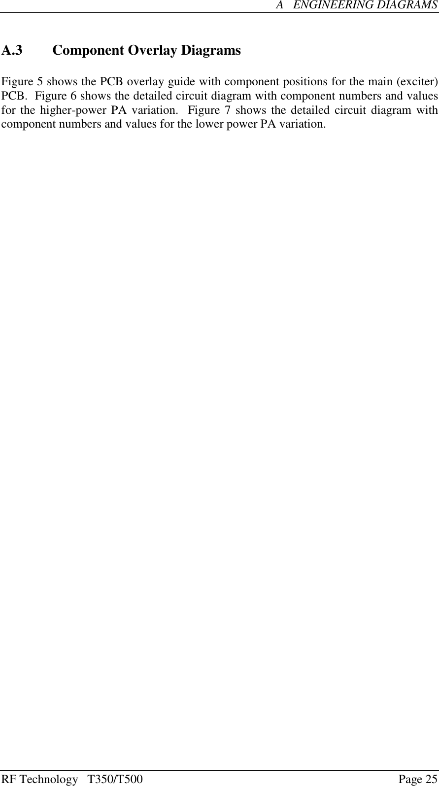
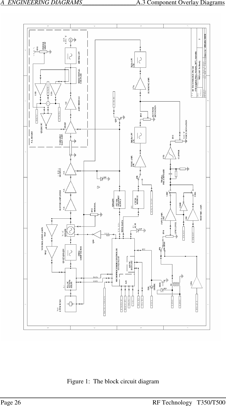
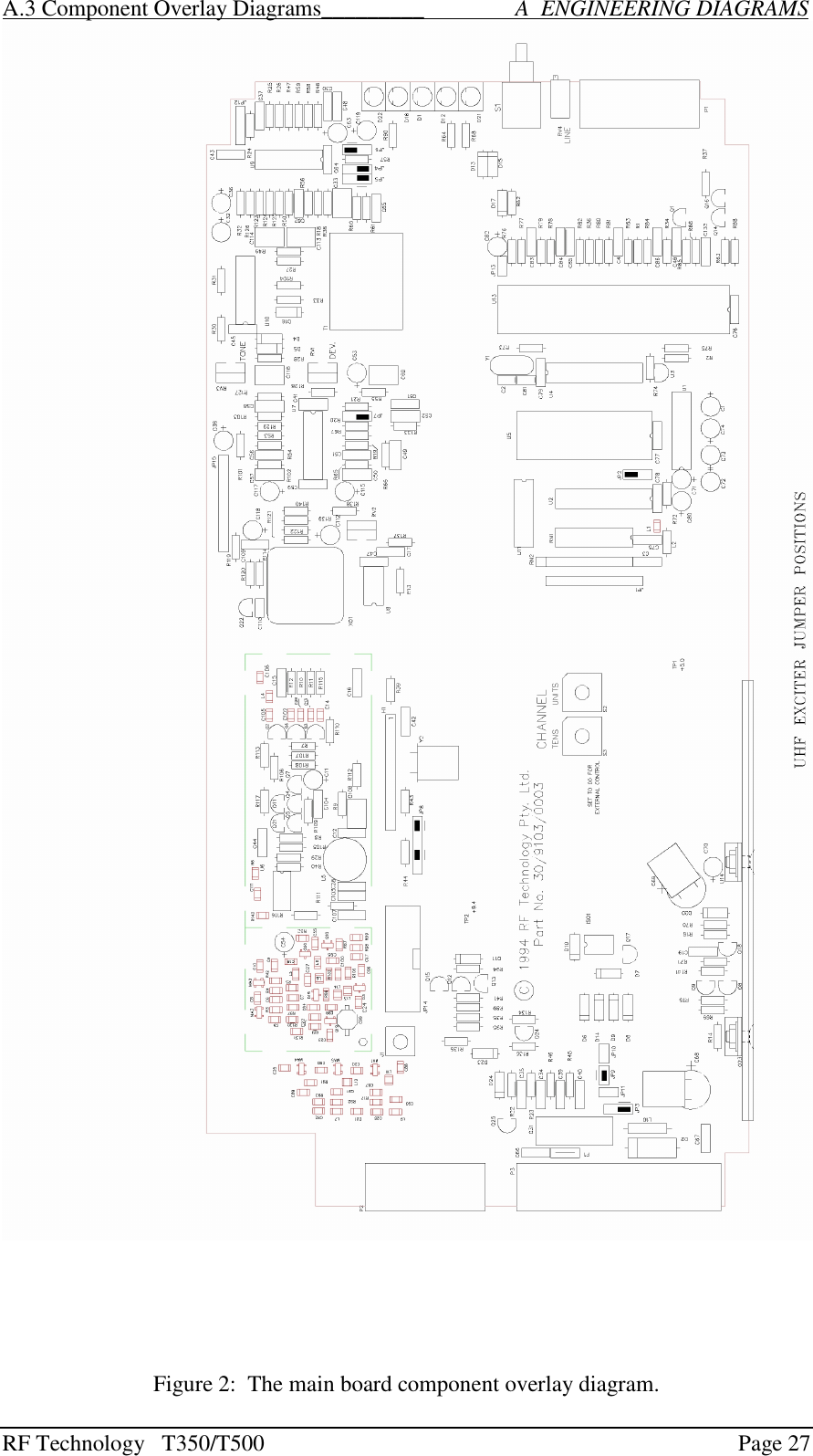
RF Technology T500A Base station transmitter User Manual Manual T350 Completed

RF Technology Pty Ltd Base station transmitter Manual T350 Completed

Equipment manual

Eclipse SeriesRF Technologyrfinfo@rftechnology.com.auAugust, 1998T350 / T500 TransmitterOperation and Maintenance ManualThis manual is produced by RF Technology Pty Ltd10/8 Leighton Place, Hornsby  NSW 2077  AustraliaCopyright © 1998 RF Technology
Page 2 RF Technology   T350/T500 CONTENTS           CONTENTSContents1Operating Instructions 51.1 Front Panel Controls and Indicators 51.1.1 PTT 51.1.2 Line 51.1.3 PWR LED 61.1.4 TX LED 61.1.5 ALARM LED 62Transmitter Internal Jumper Options 72.1 JP2:  EPROM type 72.2 JP3:  Dc Loop PTT 72.3 JP4:  Audio Input Source 72.4 JP6:  Input Level Attenuation 72.5 JP7:  Audio Response 82.6 JP8:  Sub-audible Tone source 82.7 JP9/10/11:  dc Loop Configuration 83Transmitter I/O Connections 83.1 25 Pin Connector 84Channel and Tone Frequency Programming 85Circuit Description 95.1 VCO Section 95.2 PLL Section 105.3 Power Amplifier 105.4 600Ω line Input 115.5 Direct Coupled Audio Input 115.6Local Microphone Input115.7 CTCSS and Tone Filter 115.8 Audio Signal Processing 125.9 PTT and DC Remote Control 125.10 Micro-processor Controller 135.11 Voltage Regulator 136Field Alignment Procedure 136.1 Standard Test Conditions 146.2 VCO Alignment 146.3 TCXO Calibration 146.4 Modulation Balance 156.5 Tone Deviation 156.6 Deviation 166.7Line Input Level166.8 Output Power 16
RF Technology   T350/T500Page 3CONTENTS           CONTENTS7Specifications 177.1 Overall Description 177.1.1 Channel Capacity 177.1.2 CTCSS 177.1.3 Channel Programming 177.1.4 Channel Selection 177.1.5 Micro-processor 187.2 Physical Configuration 187.3 Front Panel Controls, Indicators and Test Points 187.3.1 Controls 187.3.2 Indicators 187.3.3 Test Points 197.4 Electrical Specifications 197.4.1 Power Requirements 197.4.2Frequency Range and Channel Spacing197.4.3Frequency Synthesizer Step Size197.4.4Frequency Stability197.4.5 Number of Channels 197.4.6 Antenna Impedance 197.4.7 Output Power 197.4.8Transmit Duty Cycle207.4.9 Spurious and Harmonics 207.4.10 Carrier and Modulation Attack Time 207.4.11 Modulation 207.4.12 Distortion 207.4.13 Residual Modulation and Noise 207.4.14 600Ω Line Input Sensitivity 207.4.15 HI-Z Input 207.4.16 Test Microphone Input 217.4.17 External Tone Input 217.4.18 External ALC Input 217.4.19 T/R Relay Driver 217.4.20 Channel Select Input / Output 217.4.21 DC Remote Keying217.4.22 Programmable No-Tone Period 227.4.23 Firmware Timers 227.4.24 CTCSS 227.5 Connectors 227.5.1 Antenna Connector 227.5.2 Power and I/O Connector 247.5.3 Test Connector 24
Page 4 RF Technology   T350/T500CONTENTS CONTENTSAEngineering Diagrams 24A.1 Block Diagram 24A.2 Circuit Diagrams 24A.3Component Overlay Diagrams25BParts List 26
RF Technology   T350/T500Page 51OPERATING INSTRUCTIONS1Operating Instructions1.1 Front Panel Controls and Indicators1.1.1 PTTA front-panel push-to-talk (PTT) button is provided to facilitate bench and field testsand adjustments.   The button is a momentary action type.  When keyed, audio from theline  input is disabled so that a carrier with sub-tone is transmitted.  The front-panelmicrophone input is not enabled in this mode, but it is enabled when the PTT line onthat socket is pulled to ground.1.1.2 LineThe LINE trimpot is accessible by means of a small screwdriver from the front panel ofthe module.   It is used to set the correct sensitivity of the line and direct audio inputs.  Itis factory preset to give 60% of rated deviation with an input of 0dBm (1mW on 600Ωequivalent to 775mV RMS or about 2.2V peak-to-peak) at 1kHz. The nominal 60%deviation level may be adjusted by measuring between pins 6 and 1 on the test socket,and adjusting the pot. By this means an input sensitivity from approximately -30dBm to+10dBm may be established.An internal jumper provides a coarse adjustment step of 20dB. Between the jumper andthe trimpot, a wide range of input levels may be accommodated.WARNINGChanges or modifications not expressly approved byRF Technology could void your authority to operate thisequipment.  Specifications may vary from those given inthis document in accordance with requirements of localauthorities.    RF  Technology  equipment  is  subject  tocontinual improvement and RF Technology reserves theright  to  change  performance  and  specification  withoutfurther notice.
Page 6 RF Technology   T350/T5001.1 Front Panel Controls and Indicators                 1   OPERATING INSTRUCTIONSLED Flash Cadence Fault Condition5 flashes, pause Synthesizer unlocked4 flashes, pause Tuning voltage out of range3 flashes, pause Low forward power2 flashes, pause High reverse (reflected) power1 flash, pause Low dc supply voltageLED ON continuously Transmitter timed outTable 1:  Interpretations of LED flash cadenceIndication Fault ConditionFlashing, 8 per second Synthesizer unlockedFlashing, 4 per second Tuning voltage outside correct rangeFlashing, 2 per second Low forward powerFlashing, 1 per second High reverse powerContinuous dc supply voltage low or highTable 2:  Interpretations of LED flash speed, for early models1.1.3 POWER LEDThe PWR LED shows that the dc supply is connected to the receiver.1.1.4  TX LEDThe TX LED illuminates when the transmitter is keyed.   It will not illuminate (and anAlarm  cadence  will  be  shown)  if  the  synthesizer  becomes  unlocked,  or  the  outputamplifier supply is interrupted by the microprocessor.1.1.5 ALARM LEDThe Alarm LED can indicate several fault conditions if they are detected by the self testprogram.   The alarm indicator shows the highest priority fault present.  Receivers usingsoftware issue 5 and higher use the cadence of the LED flash sequence to indicate thealarm condition.  Refer to table 1.   Receivers using software issue 4 and lower use theLED flash rate to indicate the alarm condition.  Refer to table 2.
RF Technology   T350/T500Page 72TRANSMITTER INTERNAL JUMPER OPTIONS2Transmitter Internal Jumper OptionsIn  the  following  subsections an  asterisk  (*)  signifies  the  standard  (Ex-Factory)configuration of a jumper.2.1 JP2: EPROM TypeCondition Position27C256 2-3 *27C64 1-22.2 JP3: Dc Loop PTTThis jumper enables or disables the keying of the PTT function by means of a dc signalpassed down the 600Ω line input pair.  When enabled, JP9-JP11 control how the dcsignal is configured with respect to an internal opto-coupler.Condition Positiondc loop connected (enabled)   1-2 *dc loop not connected (bypassed)  2-32.3 JP4: Audio Input SourceEither the 600Ω or the high-Z balanced inputs may be selected.Condition Position600Ω Input 2-3 *High-impedance Input1-22.4 JP6: Input Level AttenuationThis jumper permits coarse input sensitivity to be set.Condition Position0dB attenuation 1-2 *20dB attenuation 2-3
Page 8 RF Technology   T350/T5002.5 JP7: Audio Response  4 CHANNEL AND TONE FREQUENCY PROGRAMMING2.5 JP7: Audio ResponseCondition Position750 uSec. pre-emphasis 1-2 *Flat response 2-32.6 JP8: Sub-audible Tone SourceCondition PositionInternal CTCSS 1-2, 4-5 *External input 2-3, 5-62.7 JP9/10/11: dc Loop ConfigurationThese settings are only relevant when the PTT signal is to be used across the same wiresas the audio.  Refer to setting of JP3.  They control the levels and connection into theaudio balanced line circuitry.Condition JP9 JP10 JP11Current Loop Input ON OFF OFF *12Vdc Loop source OFF ON ON3Transmitter I/O Connections3.1 25 Pin ConnectorThe  D-shell  25  pin  connector  is  the  main  interface  to  the  transmitter.  The  pinconnections are described in table 3.4Channel and Tone Frequency ProgrammingChannel  and  tone  frequency  programming  is  most  easily  accomplished  with  RFTechnology TecHelp software or the Service Monitor 2000 software.  This software canbe run on an IBM compatible PC and provides a number of additional useful facilities.DOS and 32-bit versions are available.TecHelp allows setting of the adaptive noise squelch threshold, provides a simple meansof calibrating the forward and reverse power detectors, setting the power alarm presetlevels, and enabling transmitter hang time and timeout time limits.  TecHelp can besupplied by your dealer, distributor or by contacting RF Technology directly.
RF Technology   T350/T500Page 94    CHANNEL AND TONE FREQUENCY PROGRAMMINGFunction Signal Pins Specificationdc power +12 Vdc-12 Vdc 1, 1413, 25 +11.4 to 16 VdcChannel Select 124810204080219221023112412BCD Coded0 = Open Circuitor 0 Vdc1 = +5 to +16 VdcRS232 Data InOut 152Test  and  Programming  use9600, 8 data 2 stop bits600Ω Line HighLow 206Transformer IsolatedBalanced 0dBm Output150Ω / Hybrid 719Direct PTT input 3Ground to key PTTT/R Relay driver output 16 Open collector,250mA/30VSub-Audible Tone Input + 5 >10kΩ, AC coupled- 18 (1-250Hz)High-Z Audio Input + 4 >10kΩ, AC coupled- 17 (10Hz-3kHz)External ALC input 8 <0.5V/1mA to obtain>30dB attenuation, O/Cfor maximum powerTable 3:  Pin connections and explanations for the main 25-pin, D connector.5Circuit DescriptionThe following  descriptions should be  read as an aid to understanding the  block andschematic diagrams given in the appendix of this manual.5.1 VCO SectionThe Voltage Controlled Oscillator uses a junction FET which oscillates at the requiredtransmitter output frequency.  A varactor diode is used by the PLL circuit to keep theoscillator on the desired frequency.  Transistor Q20 is used as an active filter to reducethe  noise  on  the  oscillator  supply  voltage.    The  VCO  is  keyed  ON  by  themicrocontroller through Q10.  It is keyed ON when any of the PTT inputs are active andOFF at all other times.
Page 10 RF Technology   T350/T500     5   CIRCUIT DESCRIPTION                                                  The VCO output is amplified and buffered by monolithic amplifiers MA2 and MA3before being fed to the PLL IC U6.Amplifiers MA1, MA4 and MA5 increase the VCO output to approximately 4 mW todrive the power amplifier.  MA1 is not switched on until the PLL has locked and hadtime  to  settle.    This  prevents  any  momentary  off  channel  transmission  when  thetransmitter is keyed.5.2  PLL SectionTemperature compensated crystal oscillator XO1 is the frequency reference source forthe PLL Synthesizer.  The frequency stability of XO1 is better than 1 ppm and it can besynchronized to an external reference for improved stability.  External reference optionboard 11/9119 is required when using an external reference.XO1 is frequency modulated by the processed transmit audio signal from U7b.  Thisextends the modulation capability down to a few Hz for sub-audible tones and digitalsquelch codes.  A two point modulation scheme is used with the audio also being fed tothe VCO to modulate the higher audio frequencies.The 12.8 MHz output of XO1 is amplified by Q22 to drive the reference input of thePLL synthesizer IC U6.  This IC is a single chip synthesizer which includes a 1.1 GHzpre-scaler, programmable divider, reference divider and phase/frequency detector.  Thefrequency data for U6 is supplied through serial data link by the microprocessor.The  phase  detector  output  signals  of  U6  are  used  to  control  two  switched  currentsources.  The output of the positive and negative sources (Q3 and Q6) produces thetuning  voltage  which  is  smoothed  by  the  loop  filter  components  to  bias  the  VCOvaractor diode D3.5.3 Power AmplifierThe 4 mW output from the main board connects to the power amplifier board through ashort miniature 5Ω coaxial cable.Q2 on the power amplifier board increases the signal to approximately 200 mW. Thebias current of Q2 is controlled by Q1 and the power leveling circuitry to adjust thedrive to the output module U2.U2 increases the power to 10-30 watts (depending upon options) before it is fed to thedirectional coupler, low pass filter and output connector.  The directional couplerdetects  the  forward  and  reverse  power  components  and  provides  proportional  dcvoltages which are amplified by U1a and U1b.  The forward and reverse voltages fromU1a and U1b are compared to the DC reference voltage from RV1.  The difference isamplified by U1c, Q3 and Q4.
RF Technology   T350/T500Page 115    CIRCUIT DESCRIPTION 5.3  Power AmplifierThe resulting control voltage supplies Q2 through R10, R12 and completes the powerleveling control loop.5.4 600Ω Line InputThe 600Ω balanced line input connects to line isolation transformer T1.  T1 has two150Ω primary windings which are normally connected in series for 600Ω lines.  Thedual primary windings can be used to provide DC loop PTT signaling or a 2/4 wirehybrid connection.  All four leads are available at the rear panel system connector.The secondary of T1 can be terminated with an internal 600Ω load through JP5 or leftun-terminated in high impedance applications.5.5 Direct Coupled Audio InputA high impedance (10kΩ) direct AC coupled input is available at the system connector.The direct coupled input connects to U9a which is configured as a unity gain bridgeamplifier.The bridge configuration allows audio signal inversion by interchanging the  positiveand  negative  inputs  and  minimizes  ground  loop  problems.    Both  inputs  should  beconnected, with one lead going to the source output pin and the other connected to thesource audio ground.5.6 Local Microphone InputThe local microphone input is provided for use with a standard low impedance dynamicmicrophone.  The microphone output is amplified by U9a before connecting to analogueswitch U10a.  U10b inverts the local microphone PTT input to switch U10a ON whenthe microphone PTT button is pressed.  U10a is OFF at all other times.The local microphone audio has priority over the other inputs.  Activation of the localmicrophone PTT input switches OFF the audio from the line or direct inputs throughD16 and U10c.5.7 CTCSS and Tone FilterThe CTCSS encoder module H1, under control of the main microprocessor U13, canencode all 38 EIA tones and (on some models) additional commonly-used tones.The tone output of H1 connects to jumper JP8 which is used to select either H1 or anexternal tone source.  The selected source is coupled to U9c which is a balanced inputunity gain amplifier.  The buffered tone from U9c is fed to 300 Hz low pass filter U7c.RV3, the tone deviation trimmer, is used to adjust the level of the tone
Page 12 RF Technology   T350/T5005.8  Audio Signal Processing 5   CIRCUIT DESCRIPTIONfrom U7c before it is combined with the voice audio signal in the summing amplifierU7a.Back to back diodes D4 and D5 limit the maximum tone signal amplitude to preventexcessive tone deviation when external tone sources are used.5.8 Audio Signal ProcessingJumper JP4 selects either the line or direct input source.  The selected source is thenconnected to JP6.  JP6 can be removed to provide 20 dB attenuation when the inputlevel is above 10 dBm to expand the useful range of the line level trimmer RV4.  Thewiper  of  RV4  is coupled  to the  input  of the  input amplifier  U9d.    U9d  provides  avoltage gain of ten before connecting to the input of analogue switch U10c.The  outputs  of  U10a  and  U10c  are  connected  to  the  frequency  response  shapingnetworks C52, R133 (for 750µs pre-emphasis) and C61, R55 (for flat response).  JP7selects the pre-emphasized or flat response.The  audio  signal  is  further  amplified  100  times  by  U7d.    U7d  also  provides  thesymmetrical clipping required to limit the maximum deviation.  The output level fromU7d is adjusted by RV1, the deviation adjustment, before being combined with the toneaudio signal in the summing amplifier U7a.The  composite  audio  from  U7a  is  fed  through  the  3Khz  low  pass  filter  U7b.    Thefiltered audio is coupled to the TCXO voltage tuning input and the modulation balancetrimmer RV2.RV2 adjusts level of the audio used to modulate the VCO. This primarily effects thedeviation of audio frequencies above 500 Hz.  RV2 is used to balance the high and lowfrequency  deviation  to  obtain  a  flat  frequency  response  relative  to  the  desiredcharacteristic.5.9 PTT and DC Remote ControlTwo main PTT inputs are provided.  The first, a direct logic level input, is connected topin 3 of the system connector.  The transmitter can be keyed by applying a logic low orground on pin 3.  Pin 3 connects to the PTT logic and microprocessor through D10.DC current loop control can be used for remote PTT operation.  The current loop can beconfigured by JP9, JP10 and JP11 for use with either a remote free switch or a remoteswitched source.Opto-isolator ISO1 is used to isolate the loop current signal from the transmitter PTTlogic.    The  loop  current  passes  through  the  input  of  ISO1  and  the  output  of  ISO1connects to the PTT logic.
RF Technology   T350/T500Page 135CIRCUIT DESCRIPTION 5.10  Microprocessor ControllerA bridge consisting of diodes D6, D8, D9 and D14 ensures correct operation regardlessof the current polarity.  Q17 limits the current and D7 limits the voltage input to ISO1.Any low voltage current source capable of providing 2 mA at 4 V or switching circuitwith less than 4.8kΩ loop resistance can be used to switch the DC loop.The test PTT button on the front panel and the local microphone PTT button will alsokey the transmitter.  Both of these also mute the line audio input. The microphone linealso enables that audio input.5.10 Microprocessor ControllerThe microprocessor controller circuit uses a single-chip eight bit processor and severalsupport  chips.    The  processor  U13  includes  non-volatile  EE  memory  for  channelfrequencies, tones, and other information.  It also has an asynchronous serial port, asynchronous serial port and an eight bit analogue to digital converter.The program is stored in U5, a CMOS EPROM. U4 is an address latch for the low orderaddress bits.  U2 is used to read the channel select lines onto the data bus.  U11 is anaddress decoder for U5 and U2.  U3 is a supervisory chip which keeps the processorreset  unless  the  +5  Volt  supply  is  within  operating  limits.    U1  translates  theasynchronous serial port data to standard RS232 levels.The analogue to digital converter is used to measure the forward and reverse power,tuning voltage and dc supply voltage.The processor keys the VCO through Q10, switches the 9.2 Volt transmit line throughQ14 and Q16, and the alarm LED D1 through Q1.5.11 Voltage RegulatorThe dc input voltage is regulated down to 9.4 Vdc by a discrete regulator circuit.  Theseries pass transistor Q23 is driven by error amplifiers Q8 and Q18.  Q9 is used to startup the regulator and once the circuit turns on, it plays no further part in the operation.The +5 Volt supply for the logic circuits is provided by an integrated circuit regulatorU14 which is run from the regulated 9.4 Volt supply.6Field Alignment ProcedureThe procedures given below may be used to align the transmitter in the field. Normally,alignment is only  required when changing operating frequencies, or after componentreplacement.
Page 14 RF Technology   T350/T5006FIELD ALIGNMENT PROCEDURE  6.1  Standard Test ConditionThe procedures below do not constitute an exhaustive test or a complete alignment ofthe module, but if successfully carried out are adequate in most circumstances.TCXO calibration may be periodically required owing to normal quartz crystal aging. Adrift of 1ppm/year is to be expected.Each alignment phase assumes that the preceding phase has been successfully carriedout, or  at  least that  the  module  is  already  in  properly  aligned  state  with  respect  topreceding conditions.6.1 Standard Test ConditionThe following equipment and conditions are assumed unless stated otherwise:•AF signal generator with 600Ω impedance, 150-3000Hz frequency range, with levelset to 387mV RMS.•Power supply set to 13.8Vdc, with a current capable of  >5A.•RF 50Ω load, 30W rated, return loss <-20dB.•Jumpers set to factory default positions.6.2 VCO Alignment1.Select a channel at the center frequency (half way between the highest and lowestfrequencies for the model in question).2. Disconnect the Audio input (no signal input).3.Key the PTT line.4.Measure the voltage between pins 9 and 1 of the test socket (TUNE V), and adjustC99 to obtain 4.5±0.25V, while the TX LED is ON and the ALARM LED is OFF.6.3   TCXO Calibration1.Select a channel at the center frequency (half way between the highest and lowestfrequencies for the model in question).2. Disconnect the Audio input (no signal input).3.Key the PTT line.
RF Technology   T350/T500Page 156.4  Modulation Balance 6   FIELD ALIGNMENT PROCEDURE    4.    Measure the carrier frequency at the output connector, and adjust XO1 until thecorrect carrier frequency is measured, ±50Hz.6.4 Modulation Balance1. Set RV3 fully counter clockwise (CCW)  (sub-tone off).2. Set RV1 fully clockwise (CW)  (maximum deviation)3. Set RV2 mid-position4. Set JP7 for flat response5.Key the transmitter on6. Set the audio input to 150Hz, 0dBm.7. Measure deviation and adjust RV4 (line Level) for a deviation of 5kHz (2.5kHzfor narrow band transmitters).8. Set the audio input to 1.5kHz, 0dBm.9. Adjust  RV2  (Mod.  Bal.)  for  a  deviation  of  5kHz  (2.5kHz  for  narrow  bandtransmitters).10. Repeat steps 6-9 until balance is achieved.11.Key the transmitter off.12. Return JP7 to its correct setting.13. Carry out the Deviation (section 6.6) and Tone Deviation (section 6.5) alignmentprocedures.6.5 Tone Deviation1. Remove the audio input.2.Key the transmitter on.3. Adjust  RV3  for  the  desired  deviation  in  the  range  0-1kHz.1   If  sub-tone(CTCSS) coding is not to be used, adjust RV3 fully CCW.____________________1   The factory default is 500Hz for wide band (5kHz maximum deviation) and 250Hz for narrow bandchannels.
Page 16 RF Technology   T350/T5006FIELD ALIGNMENT PROCEDURE  6.6   Deviation6.6 Deviation1. Set RV4 (Line Level) fully clockwise (CW).2. Set the audio to 1kHz, 0dBm, on the line input.3.Key the transmitter on..4. Adjust RV1 (Set Max. Deviation) for a deviation of 5kHz (2.5kHz for narrowband transmitters).5.Key the transmitter off.6.Carry out the Line Input Level alignment procedure (section 6.7)6.7 Line Input Level1. Set the audio to 1kHz, 0dBm, on the line input, or use the actual signal to betransmitted.2.Key the transmitter on.3. Adjust RV4 (line level) for 60% of system deviation (3kHz or 1.5kHz for narrowband systems).4. If the test signal is varying, RV4 may be adjusted to produce a level of 234mVRMS or 660mVp-p at the  audio voltage test connector pin 6 to pin 1.5.Key the transmitter off.6.8 Output Power1. No audio input is required2.Key the transmitter on.3.Adjust RV1 on the power amplifier PCB for the desired power level at the outputconnector. 24.Key the transmitter off.____________________2   Be sure to set the power below the rated maximum for the model of transmitter.  If in doubt, allow1.5dB cable and connector losses, and assume that the maximum rated power is 15W.  This means nomore than 10W at the end of a 1m length of test cable.  This pessimistic procedure is safe on all modelsmanufactured at the time of writing.
RF Technology   T350/T500Page 177  SPECIFICATIONS7SPECIFICATIONS7.1 Overall DescriptionThe  transmitter is  a frequency synthesized,  narrow band  FM  unit,  normally  used  todrive a 50 watt amplifier.  It can also be used alone in lower power applications.Various  models  allow  2-25W  of  output  power  to  be  set  across  a  number  of  UHFfrequency bands.  All necessary control and 600Ω line interface circuitry is included.7.1.1 Channel CapacityAlthough most applications are single channel, it can be programmed for up to  100channels,  numbered  0  -  99.    This  is  to  provide  the  capability  of  programming  allchannels into all of the transmitters used at a given site. Where this facility is used inconjunction with channel-setting in the rack, exciter modules may be “hot-jockeyed” orused interchangeably. This can be convenient in maintenance situations.7.1.2 CTCSSFull  EIA  sub-tone  capability  is  built  into  the  modules.      The  CTCSS  tone  can  beprogrammed for each channel.  This means that each channel number can represent aunique RF and tone frequency combination.7.1.3 Channel ProgrammingThe channel information is stored in non-volatile memory and can be programmed viathe front panel test connector using a PC and RF Technology software.7.1.4 Channel SelectionChannel selection is by eight channel select lines.  These are available through the rearpanel connector. Internal presetting is also possible. The default (open-circuit) state is toselect channel 00.A BCD active high code applied to the lines selects the required channel.  This can besupplied by pre-wiring the rack connector so that each rack position is dedicated to afixed channel.  Alternatively, thumb-wheel switch panels are available.
Page 18 RF Technology   T350/T5007SPECIFICATIONS 7.1.5  Microprocessor7.1.5. MicroprocessorA microprocessor is used to control the synthesizer, tone squelch, PTT function andfacilitate channel frequency programming.  With the standard software, RF Technologymodules also provide fault monitoring and reporting.7.2 Physical ConfigurationThe transmitter is designed to fit in a 19 inch rack mounted sub-frame.  The installedheight is 4 RU (178 mm) and the depth is 350 mm.  The transmitter is 63.5 mm or twoEclipse modules wide.7.3 Front Panel Controls, Indicators, and Test Points7.3.1 ControlsTransmitter Key - Momentary Contact Push ButtonLine Input Level - screwdriver adjust multi-turn pot7.3.2 IndicatorsPower ON - Green LEDTx Indicator - Yellow LEDFault Indicator - Flashing Red LEDExternal ALC - Green LEDExternal Reference - Green LED7.3.3 Test PointsLine Input - 6 + Ground (pin 1)Forward Power - 8 + Ground (pin 1)Reverse Power - 4 + Ground (pin 1)Tuning Voltage - 9 + Ground (pin 1)Serial Data (RS-232) – 2 / 3 + Ground (pin 1)
RF Technology   T350/T500Page 197.4  Electrical Specifications   7   SPECIFICATIONS7.4 Electrical Specifications7.4.1 Power RequirementsOperating Voltage - 10.5 to 16 Vdc with output power reduced below 12 VdcCurrent Drain - 5A Maximum, typically 0.25A StandbyPolarity - Negative Ground7.4.2 Frequency Range and Channel SpacingFrequency 25 kHz 12.5 kHz330-365 MHz T350C T350CN360-380 MHz T350A T350AN375-400 MHz T350B T350BN403-420 MHz T500A T500AN430-450 MHz T500D T500DN450-520 MHz T500B T500BN7.4.3 Frequency Synthesizer Step SizeStep size is 10 / 12.5kHz or 5 / 6.25kHz, fixed, depending upon model7.4.4 Frequency Stability±1 ppm over 0 to +60 C, standard±1ppm over -20 to +60 C, optional7.4.5 Number of  Channels100, numbered 00 - 997.4.6 Antenna Impedance50Ω7.4.7 Output powerPreset for 2-15 or 2-25W depending upon model
Page 20 RF Technology   T350/T5007SPECIFICATIONS 7.4.8  Transmit Duty Cycle7.4.8 Transmit Duty Cycle100% to 40C, de-rating to zero at 60C.100% to 5000ft altitude, de-rating to zero at 15,000ft.7.4.9 Spurious and HarmonicsLess than 0.25µW7.4.10   Carrier and Modulation Attack TimeLess than 20ms. Certain models have RF envelope attack and decay times controlled inthe range 200µs< tr/f <2ms according to regulatory requirements.7.4.11  ModulationType - Two point direct FM with optional pre-emphasisFrequency Response - ±1 dB of the selected characteristic from 300 - 3000 HzMaximum Deviation - Maximum deviation preset to 2.5 or 5 kHz7.4.12   DistortionModulation distortion is less than 3% at 1 kHz and 60% of rated system deviation.7.4.13   Residual Modulation and NoiseThe residual modulation and noise in the range 300 - 3000 Hz is typically less than -50dB referenced to rated system deviation.7.4.14  600Ω Line Input SensitivityAdjustable from -30 to +10 dBm for rated deviation7.4.15 HI-Z InputImpedance  - 10KΩ Nominal, balanced inputInput Level  -  25mV to 1V RMS
RF Technology   T350/T500Page 217.4.16  Test Microphone Input 7  SPECIFICATIONS7.4.16   Test Microphone Input200Ω dynamic, with PTT7.4.17   External Tone InputCompatible with R500 tone output7.4.18   External ALC InputOutput will be reduced 20dB by pulling the input down to below 1V.  (Typically morethan 40dB attenuation is available.)  The input impedance is ≅10kΩ, internally pulledup to rail.The  external  ALC  input  can  be  connected  to  the  power  control  circuit  in  Eclipseexternal power amplifiers.7.4.19   T/R Relay DriverAn open collector transistor output is provided to operate an antenna change over relayor solid state switch.  The transistor can sink up to 250mA.7.4.20 Channel Select Input / OutputCoding - 8 lines, BCD coded 00 - 99Logic Input Levels - Low for <1.5V, High for >3.5VInternal 10K pull down resistors select channel 00 when all inputs are O/C.7.4.21   DC Remote KeyingAn opto-coupler input is provided to enable dc loop keying over balanced lines or localconnections.  The circuit can be connected to operate through the 600Ω line or througha separate isolated pair.
Page 22 RF Technology   T350/T5007SPECIFICATIONS 7.4.22  Programmable No-Tone Period7.4.22 Programmable No-Tone PeriodA No-Tone period can be appended to the end of each transmission to aid in eliminatingsquelch tail noise which may be heard in mobiles with slow turn off decoders.  The No-Tone period can be set  from 0--5  seconds in 0.1 second  increments.   The No Toneperiod operates in addition to the reverse phase burst at the end of each transmission.37.4.23 Firmware TimersThe controller firmware includes some programmable timer functions.Repeater Hang Time - A short delay or ``Hang Time'' can be programmed to be addedto the end of transmissions.  This is usually used in talk through repeater applications toprevent the repeater from dropping out between mobile transmissions.  The Hang Timecan be individually set on each channel for 0 - 15 seconds.Time Out Timer  -  A  time-out  or  transmission  time  limit  can  be  programmed  toautomatically turn the transmitter off.  The time limit can be set from 0-254 minutesin increments of one minute.  The timer is automatically reset when the PTT input isreleased.7.4.24 CTCSSCTCSS tones can be provided by an internal encoder or by an external source connectedto the external tone input.  The internal CTCSS encoding is provided by a subassemblyPCB module.  This provides programmable encoding of all EIA tones.Some models encode certain extra tones.Tone frequencies are given in table 4.7.5 Connectors7.5.1 Antenna ConnectorType N Female Mounted on the module rear panel3  The reverse phase burst is usually sufficient to eliminate squelch tail noise in higher-quality mobiles.
RF Technology   T350/T500Page 237   SPECIFICATIONSFrequency EIA NumberNo Tone67.0 A169.471.9 B174.4 C177.0 A279.7 C282.5 B285.4 C388.5 A391.5 C494.8 B397.4100.0 A4103.5 B4107.2 A5110.9 B5114.8 A6118.8 B6123.0 A7127.3 B7131.8 A8136.5 B8141.3 A9146.2 B9151.4 A10156.7 B10159.8162.2 A11165.5167.9 B11171.3173.8 A12177.3179.9 B12183.5186.2 A13189.9192.8 B13196.6199.5203.5 A14206.5210.7 B14218.1 A15225.7 B15229.1233.6 A16241.8 B16250.3 A17254.1Table 4:  Tone Squelch Frequencies
Page 24 RF Technology   T350/T500AENGINEERING DIAGRAMS7.5.2 Power & I/O Connector25-pin “D” Male Mounted on the rear panel7.5.3 Test Connector9-pin  “D” Female mounted on the front panelAEngineering DiagramsMost Eclipse transmitter modules contain two PCBs, a motherboard with the controland signal generation circuitry (the exciter board), and an RF Power Amplifier board.Certain  models  are  equipped  with  optional  functions  on  piggyback  PCBs  atop  theexciter motherboard.  The exciter PCB typically has a few components whose valuesvary from model to model depending upon operating frequency and local regulatoryconstraints. The RF PA PCB varies from model to model but to a greater extent.  Atleast two different PCB layouts, and numerous variations, exist.  This manual presentsthe circuits and parts lists for two representative variants. When ordering spare parts besure to specify the model exactly, in case the part you require is different in value fromthat specified in this manual.Older models (predating this manual) may not be covered by this manual.  However,advances are evolutionary, and the information in this manual will be sufficient in mostcases to permit understanding and servicing of all models, past and present.Versions of more detailed circuit schematics, printed on A3 paper, may be inserted orbound with this manual towards the end.  It is sometimes easier to work with these fold-out diagrams because of their larger format.  In case the inserts / fold-outs are missingor damaged, the reader is advised that information in the figures included with the textshould be identical.A.1 Block DiagramFigure 1 shows the block signal flow diagram.A.2 Circuit DiagramsFigure 2 shows the detailed circuit diagram with component numbers and values for themain  (exciter)  PCB.    Figure  3  shows  the  detailed  circuit  diagram  with  componentnumbers and values for the higher-power PA variation.  Figure 4 shows the detailedcircuit diagram with component numbers and values for the lower-power PA variation.
RF Technology   T350/T500Page 25A   ENGINEERING DIAGRAMSA.3 Component Overlay DiagramsFigure 5 shows the PCB overlay guide with component positions for the main (exciter)PCB.  Figure 6 shows the detailed circuit diagram with component numbers and valuesfor the higher-power PA variation.  Figure 7 shows the detailed circuit diagram withcomponent numbers and values for the lower power PA variation.
Page 26 RF Technology   T350/T500A  ENGINEERING DIAGRAMS_________________A.3 Component Overlay DiagramsFigure 1:  The block circuit diagram
RF Technology   T350/T500Page 27A.3 Component Overlay Diagrams_________                A  ENGINEERING DIAGRAMSFigure 2:  The main board component overlay diagram.
Page 28 RF Technology   T350/T500A  ENGINEEERING DIAGRAMS                               A.3 Component Overlay DiagramsFigure 3: The component circuit diagram of the 9103 UHF Transmitter.
RF Technology   T350/T500Page 29This Page Is Blank Intentionally
Page 30 RF Technology   T350/T500A  ENGINEEERING DIAGRAMS                               A.3 Component Overlay DiagramsFigure 4:  The component circuit diagram of the 9102 UHF PA.
RF Technology   T350/T500Page 31A.3 Component Overlay Diagrams                                  A  ENGINEERING DIAGRAMSFigure 5:  The component circuit diagram of the 9128/9149 UHF PA.
Page 32 RF Technology   T350/T500A  ENGINEERING DIAGRAMS                                 A.3  Component Overlay DiagramsFigure 6:  The component overlay diagram for the higher-power PA board.
RF Technology   T350/T500Page 33A.3 Component Overlay Diagrams                                  A  ENGINEERING DIAGRAMSFigure 7:  The component overlay diagram for the lower-power PA board
Page 34 RF Technology   T350/T500B  PARTS LIST                                                                                T350/T500 Parts ListB     T350/T500 Parts List (for PCB-30/9103/xxxx)Main PCB Assembly PartsRef. Description Part NumberC1       Capacitor 10U 35V Rad Electro      41/2001/010UC2       Capacitor 18P 2% 100V NPO Rad.1    45/2680/018PC3       Capacitor 100N 10% 50V X7R Rad.2    46/2001/100NC4       Capacitor 10N 10% 50V X7R Rad.2    46/2001/010NC5       Capacitor 1N0 5% 63V NPO SM1206  46/3300/01N0C6       Capacitor 1N0 5% 63V NPO SM1206  46/3300/01N0C7       Capacitor 1N0 5% 63V NPO SM1206  46/3300/01N0C8       Capacitor 1N0 5% 63V NPO SM1206  46/3300/01N0C9       Capacitor 1N0 5% 63V NPO SM1206  46/3300/01N0C10      Capacitor 1N0 5% 63V NPO SM1206   46/3300/01N0C11      Capacitor 10U 35V Rad Electro      41/2001/010UC12      Capacitor 47N 20% 50V X7R Rad.2     46/2001/047NC13      Capacitor 1N0 5% 63V NPO SM1206   46/3300/01N0C14      Capacitor 1N0 5% 63V NPO SM1206   46/3300/01N0C15      Capacitor 10N 10% 50V X7R Rad.2    46/2001/010NC16      Capacitor 10N 10% 50V X7R Rad.2    46/2001/010NC17      Capacitor 10N 10% 50V X7R Rad.2    46/2001/010NC18      Capacitor 1N0 5% 63V NPO SM1206   46/3300/01N0C19      Capacitor 100N 10% 50V X7R Rad.2    46/2001/100NC20      Capacitor 1N0 5% 63V NPO SM1206   46/3300/01N0C21      Capacitor 100N 10% 63V X7R 1206    46/3310/100NC22      Capacitor 3P3 5% 63V NPO SM1206    46/3300/03P3C23      Capacitor 1N0 5% 63V NPO SM1206   46/3300/01N0C24      Capacitor 2P7 5% 63V NP0 SM1206    46/3300/02P7C25      Capacitor 1N0 5% 63V NPO SM1206   46/3300/01N0C26      Capacitor, 6.8U SMD Tantalum  42/3009/06U8C27      Capacitor 1N0 5% 63V NPO SM1206   46/3300/01N0C28      Capacitor 1N0 5% 100V NPO Rad.2    46/2000/01N0C29      Capacitor 1N0 5% 63V NPO SM1206   46/3300/01N0C30      Capacitor 100N 10% 50V X7R Rad.2    46/2001/100NC31      Capacitor 2U2 10% 100V MKT Rad.2    47/2010/02U2C32      Capacitor 10U 35V Rad Electro      41/2001/010UC33      Capacitor 1UO 10% 63V MKT Rad.2    47/2007/01U0C34      Capacitor 1N0 5% 100V NPO Rad.2    46/2000/01N0C35      Capacitor 1N0 5% 100V NPO Rad.2    46/2000/01N0C36      Capacitor 10U 35V Rad Electro      41/2001/010UC37      Capacitor 1N0 5% 100V NPO Rad.2    46/2000/01N0C38      Capacitor 10U 35V Rad Electro      41/2001/010UC39      Capacitor 1N0 5% 100V NPO Rad.2    46/2000/01N0C40      Capacitor 1N0 5% 100V NPO Rad.2    46/2000/01N0C41      Capacitor 100N 5% 50V MKT Rad.2     47/2007/100NC42      Capacitor 100N 10% 50V X7R Rad.2    46/2001/100NC43      Capacitor 1N0 5% 100V NPO Rad.2    46/2000/01N0C44      Capacitor 10N 10% 50V X7R Rad.2    46/2001/010NC45      Capacitor 1N0 5% 100V NPO Rad.2    46/2000/01N0C46      Capacitor 10N 10% 50V X7R Rad.2    46/2001/010NC47s      Capacitor 1N0 5% 63V NPO SM1206 46/3300/01N0C48      Capacitor 100N 10% 50V X7R Rad.2    46/2001/100NC49      Capacitor 22N 5% 63V MKT Rad.2     47/2010/022NC50      Capacitor 100N 5% 50V MKT Rad.2     47/2007/100NC51      Capacitor 1N2 5% NPO Rad.2        46/2000/01N2C52      Capacitor 1N5 10% 50V COG Rad.2    46/2000/01N5C53      Capacitor 1U 35V Rad Electro       41/2001/001UC54      Capacitor 10U 35V Rad Electro        41/2001/010UC55      Capacitor 10N 10% 63V X7R SM1206    46/3310/010N
RF Technology   T350/T500Page 35B   T350/T500 PARTS LISTRef. Description Part NumberC56      Capacitor 1N2 5% NPO Rad.2         46/2000/01N2C57      Capacitor 100N 5% 50V MKT Rad.2     47/2007/100NC58      Capacitor 22N 5% 63V MKT Rad.2     47/2010/022NC59s  Capacitor 1N0 5% 63V NPO SM1206  46/3300/01N0C60      Capacitor 1UO 10% 63V MKT Rad.2  47/2007/01U0C61      Capacitor 100N 10% 50V X7R Rad.2    46/2001/100N    C62      Capacitor 100N 10% 50V X7R Rad.2    46/2001/100NC63      Capacitor 10U 35V Rad Electro    41/2001/010UC64s  Capacitor 1N0 5% 63V NPO SM1206  46/3300/01N0 C65      Capacitor 1N0 5% 100V NPO Rad.2  46/2000/01N0C66      Capacitor 100N 10% 50V X7R Rad.2    46/2001/100NC67      Capacitor 100N 10% 50V X7R Rad.2    46/2001/100NC68      Capacitor 470U 25V RB Electro      41/2001/470UC69      Capacitor 470U 25V RB Electro      41/2001/470UC70      Capacitor 10U 35V Rad Electro     41/2001/010UC71      Capacitor 10U 35V Rad Electro    41/2001/010UC72      Capacitor 10U 35V Rad Electro     41/2001/010UC73     Capacitor 10U 35V Rad Electro    41/2001/010UC74      Capacitor 10U 35V Rad Electro     41/2001/010UC75      Capacitor 1N0 5% 100V NPO Rad.2  46/2000/01N0C76      Capacitor 1N0 5% 100V NPO Rad.2   46/2000/01N0C77      Capacitor 100N 10% 50V X7R Rad.2    46/2001/100NC78      Capacitor 100N 10% 50V X7R Rad.2    46/2001/100NC79      Capacitor 100N 10% 50V X7R Rad.2    46/2001/100NC80      Capacitor 10U 35V Rad Electro     41/2001/010UC81      Capacitor 18P 2% 100V NPO Rad.1   45/2680/018PC82      Capacitor 10U 35V Rad Electro    41/2001/010UC83      Capacitor 10N 10% 50V X7R Rad.2    46/2001/010NC84      Capacitor 10N 10% 50V X7R Rad.2    46/2001/010NC85      Capacitor 10N 10% 50V X7R Rad.2    46/2001/010N    C86      Capacitor 10N 10% 50V X7R Rad.2    46/2001/010NC87      Capacitor 100N 10% 63V X7R 1206    46/3310/100NC88      Capacitor 10P 5% 63V NPO SM1206  46/3300/010PC89      Capacitor 100N 10% 63V X7R 1206    46/3310/100N      C90      Capacitor 10P 5% 63V NPO SM1206  46/3300/010PC91       Capacitor 100N 10% 63V X7R 1206    46/3310/100NC92      Capacitor 1N0 5% 63V NPO SM1206  46/3300/01N0C93      Capacitor 100N 10% 63V X7R 1206    46/3310/100N       C94      Capacitor 1P8 5% 63V NPO SM1206  46/3300/01P8C95      Capacitor 100N 10% 63V X7R 1206    46/3310/100NC96      Capacitor 1N0 5% 63V NPO SM1206  46/3300/01N0C97      Capacitor 1N0 5% 63V NPO SM1206  46/3300/01N0     C98      Capacitor 1P8 5% 63V NPO SM1206  46/3300/01P8C99      Capacitor Trim 5-25P               49/3002/025PC100     Capacitor 1N0 5% 63V NPO SM1206   46/3300/01N0C101     Capacitor 1N0 5% 63V NPO SM1206   46/3300/01N0C102     Capacitor 10N 10% 63V X7R 1206     46/3310/010NC103     Capacitor 47N 20% 50V X7R Rad.2     46/2001/047NC104     Capacitor 100N 10% 50V X7R Rad.2    46/2001/100NC105     Capacitor 1N0 5% 63V NPO SM1206   46/3300/01N0C106     Capacitor 100N 10% 63V X7R 1206    46/3310/100NC107     Capacitor 47N 20% 50V X7R Rad.2     46/2001/047NC108     Capacitor 1UO 10% 63V MKT Rad.2    47/2007/01U0C109     Capacitor 10N 10% 50V X7R Rad.2    46/2001/010N       C110     Capacitor 47P 2% 100V NPO Rad.1    45/2680/047PC111     Capacitor 100N 10% 63V X7R 1206    46/3310/100NC112     Capacitor 100U 25V RB Electro      41/1025/100UC113 Capacitor 1UO 10% 63V MKT Rad.2    47/2007/01U0
Page 36 RF Technology   T350/T500B    T350/T500 PARTS LISTRef. Description Part NumberC114     Capacitor 1UO 10% 63V MKT Rad.2    47/2007/01U0C115     Capacitor 100U 25V RB Electro      41/1025/100UC116     Capacitor 1UO 10% 63V MKT Rad.2    47/2007/01U0C117     Capacitor 100U 25V RB Electro      41/1025/100UC118     Capacitor 10U 35V Rad Electro      41/2001/010UC119     Capacitor 10U 35V Rad Electro      41/2001/010UC132 Capacitor 10N 10% 50V X7R Rad.2    46/2001/010ND1       Diode LED Red T1 3/4         21/1010/LEDRD2       Diode 3Amplifier 1KV Rectifier  21/1080/5408D3       Diode VCapacitor MMBV105G SOT23   21/3060/105GD4       Diode Silicon 1N4148         21/1010/4148D5 Diode Silicon 1N4148 21/1010/4148D6       Diode Silicon GP                 21/1010/4002D7       Diode Zen 1N4751 30V 1W AXIAL    21/1040/4751D8       Diode Silicon GP                 21/1010/4002D9       Diode Silicon GP                 21/1010/4002     D10      Diode Silicon 1N4148         21/1010/4148D11      Diode Silicon 1N4148         21/1010/4148D12      Diode LED Yellow T1 3/4      21/1010/LEDYD13      Diode Silicon 1N4148         21/1010/4148D14      Diode Silicon GP                 21/1010/4002D15      Diode Silicon 1N4148         21/1010/4148D16      Diode Silicon 1N4148         21/1010/4148D17      Diode Silicon 1N4148         21/1010/4148D18      Diode LED Green T1 3/4       21/1010/LEDGD19      Diode Schottkey BAT17 SOT23        21/3030/0017D20      Diode 8V2 Zener              21/1040/B8V2D21      Diode LED Green T1 3/4       21/1010/LEDGD22      Diode LED Green T1 3/4       21/1010/LEDGD23      Diode Silicon 1N4148         21/1010/4148D24      Diode Zen 1N4751 30V 1W AXIAL   21/1040/4751D25(L9) SMD Diode, 100ma 50v         21/3009/AS85H1       Hybred CTCSS                 13/9150/0002ISO1     IC Opto-Isolator 4N33        25/1010/4N33J1       Connector Coax SKT SMB Vertical PCB  35/2004/0001JP2      Connector 3Way Header              35/2501/0003JP3      Connector 3Way Header              35/2501/0003JP4      Connector 3Way Header              35/2501/0003JP5      Connector 3Way Header              35/2501/0003JP6      Connector 3Way Header              35/2501/0003JP7      Connector 3Way Header              35/2501/0003JP8      Connector 6Way Header              35/2501/0006JP9      Connector 2Way Header              35/2501/0002JP10     Connector 2Way Header              35/2501/0002JP11     Connector 2Way Header              35/2501/0002JP13     Connector 2Way Header              35/2501/0002JP14     Connector 16Way Shr'd Header    35/2502/0016JP15     Connector 10Way Header             35/2501/0010L1       Ferrite Bead SMD             37/3321/LM31L2       Inductor 1uH Axial           37/2021/001UL3       Ferrite Bead SMD             37/3321/LM31L4       Ferrite Bead SMD             37/3321/LM31L5       Inductor 150mH 10RBH         37/2021/1RBHL6       Inductor 220N 10% Choke SM1206  37/3320/220NL7       Ferrite Bead SMD             37/3321/LM31L8       Ferrite Bead SMD             37/3321/LM31L10      Inductor 6 Hole Ferrite RFC       37/1021/0001L11      Inductor 220N 10% Choke SM1206 37/3320/220NL12      Inductor 220N 10% Choke SM1206  37/3320/220NL13      Inductor 220N 10% Choke SM1206  37/3320/220N
RF Technology   T350/T500Page 37B   T350/T500 PARTS LISTRef. Description Part NumberL14      Inductor 220N 10% Choke SM1206  37/3320/220NMA1      Amplifier MMIC MWA0311L SOT143 24/3010/0311MA2      Amplifier MMIC MWA0311L SOT143 24/3010/0311MA3      Amplifier MMIC MWA0311L SOT143 24/3010/0311MA4      Amplifier MMIC VAM-6 SOT143 24/3010/VAM6MA5      Amplifier MMIC MWA0311L SOT143  24/3010/0311P1       Filter D RT AGL 9W F Ferrite    35/5012/009FP3       Filter D RT AGL 25W M Ferrite   35/5012/025MQ1       Transistor GP NPN MMBT3904 SOT23  27/3020/3904Q2       Transistor GP NPN MMBT3904 SOT23  27/3020/3904Q3       Transistor GP PNP MMBT3906 SOT23     27/3010/3906Q4       Fast Switching SMD Transistor         27/3010/5771Q5       Transistor GP NPN MMBT3904 SOT23  27/3020/3904   Q6       Transistor GP NPN MMBT3904 SOT23  27/3020/3904   Q7       Transistor GP PNP MMBT3906 SOT23     27/3010/3906Q8       Transistor GP NPN MMBT3904 SOT23  27/3020/3904   Q9       SMD FET NJ MMBF5459LT1 SOT23          27/3020/5459Q10      Transistor GP NPN MMBT2369 SOT23 27/3020/2369Q11      Transistor GP NPN MMBT2369 SOT23   27/3010/2369Q12      Transistor GP PNP MMBT3906 SOT23     27/3010/3906Q13      Transistor GP NPN MMBT3904 SOT23  27/3020/3904Q14      Transistor GP NPN MMBT3904 SOT23  27/3020/3904Q15      Transistor GP NPN MMBT3904 SOT23  27/3020/3904Q16      Transistor GP PNP MMBT3906 SOT23     27/3010/3906Q17      SMD FET NJ MMBF5459LT1 SOT23          27/3020/5459Q18      Transistor GP NPN MMBT3904 SOT23  27/3020/3904   Q19      FET NJ MMBFJ309 SOT23   27/3030/J309Q20      Transistor GP NPN MMBT3904 SOT23  27/3020/3904Q21      Fast Switching SMD Transistor         27/3010/5771Q22      Transistor GP NPN MMBT2369 SOT23 27/3020/2369Q23      Transistor PNP MJF6107 TO22O      27/2010/6107Q24      Transistor GP PNP MMBT3906 SOT23     27/3010/3906Q25      Transistor NPN GP MPSA06 TO92   27/2010/PA06R1       Resistor 5K11 1% 0.25W Axial      51/1010/5K11R2       Resistor 4K7 5% 0.25W Axial       51/1040/04K7R3       Resistor 100 5% 0.25W SM1206      51/3380/0100R4       Resistor 100 5% 0.25W SM1206      51/3380/0100R5       Resistor 100 5% 0.25W SM1206      51/3380/0100R6       Resistor 15R 5% 0.25W SM1206      51/3380/0015R7       Resistor 68 5% 0.25W Axial        51/1040/0068R8       Resistor 3K3 5% 0.25W Axial       51/1040/03K3R9       Resistor 1K0 5% 0.25W Axial       51/1040/01K0R10      Resistor 1K0 5% 0.25W Axial       51/1040/01K0R11      Resistor 1K0 5% 0.25W Axial       51/1040/01K0R12 Resistor 1K0 5% 0.25W Axial 51/1040/01K0R13      Resistor 1K0 5% 0.25W Axial       51/1040/01K0R14      Resistor 680 5% 0.25W Axial       51/1040/0680R15      Resistor 6K8 5% 0.25W Axial       51/1040/06K8R16      Resistor 680 5% 0.25W Axial       51/1040/0680R17      Resistor 270 5% 0.25W SM1206      51/3380/0270R18      Resistor 10K 5% 0.25W Axial       51/1040/010KR19      Resistor 47K 5% 0.25W Axial       51/1040/047KR20      Resistor 1M0 5% 0.25W Axial       51/1040/01M0R21      Resistor 10K 5% 0.25W Axial       51/1040/010KR22      Resistor 10K 5% 0.25W Axial       51/1040/010KR23      Resistor 10K 5% 0.25W Axial       51/1040/010KR24      Resistor 330 5% 0.25W Axial       51/1040/0330R25      Resistor 330 5% 0.25W Axial       51/1040/0330R26      Resistor 18K 5% 0.25W Axial       51/1040/018KR27      Resistor 10K0 1% 0.25W Axial      51/1010/010K
Page 38 RF Technology   T350/T500B    T350/T500 PARTS LISTRef. Description Part NumberR28      Resistor 10K 5% 0.25W Axial       51/1040/010KR29      Resistor 2K2 5% 0.25W Axial       51/1040/02K2R30      Resistor 470K 5% 0.25W Axial     51/1040/470KR31      Resistor 10K 5% 0.25W Axial       51/1040/010KR32      Resistor 10K 5% 0.25W Axial       51/1040/010KR33      Resistor 10K 5% 0.25W Axial       51/1040/010KR34      Resistor 100K 5% 0.25W Axial      51/1040/100KR35      Resistor 100K 5% 0.25W Axial      51/1040/100KR36      Resistor 5K11 1% 0.25W Axial      51/1010/5K11R37      Resistor 10K 5% 0.25W Axial       51/1040/010KR38     Resistor 91K 5% 0.25W Axial       51/1040/091KR39      Resistor 22 5% 0.25W Axial        51/1040/0022R40      Resistor 4K7 5% 0.25W Axial       51/1040/04K7R41      Resistor 2K2 5% 0.25W Axial       51/1040/02K2R42      Resistor 100 5% 0.25W SM1206      51/3380/0100R43      Resistor 100K 5% 0.25W Axial      51/1040/100KR44      Resistor 6K8 5% 0.25W Axial       51/1040/06K8R45      Resistor 10K 5% 0.25W Axial       51/1040/010KR46      Resistor 10K 5% 0.25W Axial       51/1040/010KR47      Resistor 64K9 1% 0.25W Axial      51/1010/64K9R48      Resistor 64K9 1% 0.25W Axial      51/1010/64K9R49      Resistor 7K50 1% 0.25W Axial      51/1010/07K5R50      Resistor 1M0 5% 0.25W Axial       51/1040/01M0R51      Resistor 10K 5% 0.25W SM1206      51/3380/010KR52      Resistor 10K 5% 0.25W SM1206      51/3380/010KR53      Resistor 7K50 1% 0.25W Axial      51/1010/07K5R54      Resistor 10K0 1% 0.25W Axial      51/1010/010KR55      Resistor 91K 5% 0.25W Axial       51/1040/091KR56      Resistor 100K 5% 0.25W Axial      51/1040/100KR57      Resistor 91K 5% 0.25W Axial       51/1040/091KR58      Resistor 64K9 1% 0.25W Axial      51/1010/64K9R59      Resistor 64K9 1% 0.25W Axial      51/1010/64K9R60      Resistor 1K2 5% 0.25W Axial       51/1040/01K2R61      Resistor 1K2 5% 0.25W Axial       51/1040/01K2R62      Resistor 10K 5% 0.25W Axial       51/1040/010KR63      Resistor 4K7 5% 0.25W Axial       51/1040/04K7R64      Resistor 390 5% 0.25W Axial       51/1040/0390R65      Resistor 47K 5% 0.25W Axial       51/1040/047KR66      Resistor 47K 5% 0.25W Axial       51/1040/047KR67      Resistor 10K 5% 0.25W Axial       51/1040/010KR68      Resistor 680 5% 0.25W Axial       51/1040/0680R69      Resistor 1K 5% 0.25W Axial       51/1040/01K0R70      Resistor 680 5% 0.25W Axial       51/1040/0680R71      Resistor 4K7 5% 0.25W Axial       51/1040/04K7R72      Resistor 47 5% 0.25W Axial        51/1040/0047R73      Resistor 10M 5% 0.25W Axial       51/1040/010MR74      Resistor 4K7 5% 0.25W Axial       51/1040/04K7R75      Resistor 4K7 5% 0.25W Axial       51/1040/04K7R76      Resistor 10K 5% 0.25W Axial       51/1040/010KR77      Resistor 1K0 5% 0.25W Axial       51/1040/01K0R78      Resistor 6K49 1% 0.25W Axial      51/1010/6K49R79      Resistor 28K7 1% 0.25W Axial      51/1010/28K7R80      Resistor 5K11 1% 0.25W Axial      51/1010/5K11R81      Resistor 5K11 1% 0.25W Axial      51/1010/5K11R82      Resistor 5K11 1% 0.25W Axial      51/1010/5K11R83      Resistor 5K11 1% 0.25W Axial      51/1010/5K11R84      Resistor 100K 5% 0.25W Axial      51/1040/100KR85      Resistor 2K2 5% 0.25W Axial       51/1040/02K2R86      Resistor 680 5% 0.25W Axial       51/1040/0680
RF Technology   T350/T500Page 39B   T350/T500 PARTS LISTRef. Description Part NumberR87      Resistor 2K2 5% 0.25W SM1206      51/3380/02K2R88      Resistor 1K0 5% 0.25W Axial       51/1040/01K0R89      Resistor 10K 5% 0.25W Axial       51/1040/010K   R90      Resistor 180 5% 0.25W Axial       51/1040/0180R91      Resistor 100 5% 0.25W SM1206     51/3380/0100R92      Resistor 180 5% 0.25W SM1206      51/3380/0180R93      Resistor 270R 5% 0.25W SM1206      51/3380/0270   R94      Resistor 1K8 5% 0.25W Axial       51/1040/01K8R95      Resistor 1K0 5% 0.25W Axial       51/1040/01K0R96      Resistor 15R 5% 0.25W SM1206      51/3380/0015R97      Resistor 470R 5% 0.25W SM1206      51/3380/0470    R98      Resistor 47R 5% 0.25W SM1206      51/3380/0047R99      Resistor 10K 5% 0.25W SM1206      51/3380/010KR100     Resistor 47R 5% 0.25W SM1206      51/3380/0047R101     Resistor 4K32 1% 0.25W Axial      51/1010/4K32    R102     Resistor 4K32 1% 0.25W Axial      51/1010/4K32R103     Resistor 4K32 1% 0.25W Axial      51/1010/4K32R104     Resistor 470K 5% 0.25W Axial      51/1040/470KR105     Resistor 1K0 5% 0.25W Axial       51/1040/01K0    R106     Resistor 560 5% 0.25W Axial       51/1040/0560R107     Resistor 3K3 5% 0.25W Axial       51/1040/03K3R108     Resistor 560 5% 0.25W Axial       51/1040/0560R109     Resistor 1K0 5% 0.25W Axial       51/1040/01K0    R110     Resistor 100 5% 0.25W Axial       51/1040/0100R111     Resistor 2K2 5% 0.25W Axial       51/1040/02K2R112     Resistor 220K 5% 0.25W Axial     51/1040/220KR113     Resistor 68 5% 0.25W Axial        51/1040/0068R114     Resistor 47K 5% 0.25W Axial       51/1040/047KR115     Resistor 1K0 5% 0.25W Axial       51/1040/01K0R116     Resistor 10K 5% 0.25W Axial       51/1040/010KR117     Resistor 1K0 5% 0.25W Axial       51/1040/01K0R119     Resistor 22 5% O.25W Axial        51/1040/0022R120     Resistor 220 5% 0.25W Axial      51/1040/0220R121     Resistor 120K 5% 0.25W Axial      51/1040/120KR123     Resistor 150K 5% 0.25W Axial      51/1040/150KR124     Resistor 150K 5% 0.25W Axial      51/1040/150KR125     Resistor 680K 5% 0.25W Axial      51/1040/680KR126     Resistor 680K 5% 0.25W Axial      51/1040/680KR127     Resistor 470K 5% 0.25W Axial      51/1040/470KR128     Resistor 560K 5% 0.25W Axial      51/1040/560KR129     Resistor 470K 5% 0.25W Axial      51/1040/470KR130     Resistor 470 5% 0.25W SM1206      51/3380/0470R131     Resistor 47R 5% 0.25W SM1206      51/3380/0047R132     Resistor 47R 5% 0.25W SM1206      51/3380/0047R133     Resistor 510K 5% 0.25W Axial      51/1040/510KR134     Resistor 270 5% 0.25W Axial       51/1040/0270R135     Resistor 470 5% 0.25W Axial       51/1040/0470R136     Resistor 1K0 5% 0.25W Axial       51/1040/01K0R137     Resistor 10K 5% 0.25W Axial       51/1040/010KR138     Resistor 22K 5% 0.25W Axial       51/1040/022KR139     Resistor 4K7 5% 0.25W Axial       51/1040/04K7R140     Resistor 100K 5% 0.25W Axial      51/1040/100KR141     Resistor 10R 5% 0.25W Axial      51/1040/0010R142     Resistor 470K 5% 0.25W SM1206      51/3380/470KRN1      Resistor Pack 100K X8 DIP16       52/2002/100KRN2      Resistor Pack 10K SIP10           52/2002/010KRV1      Trimpot 10K 1 Turn Vertical    53/1020/010KRV2      Trimpot 10K 1 Turn Vertical    53/1020/010KRV3      Trimpot 10K 1 Turn Vertical    53/1020/010KRV4      Trimpot 10K Multi-turn Horizontal 53/2060/010K
Page 40 RF Technology   T350/T500B   T350/T500 PARTS LISTRef. Description Part NumberS1       Switch PSH BTN SPDT & Capacitor  31/0005/E121T1       Transformer Line 600 Ohm  37/2040/5065U1       IC RS232 Inter MAX232C       26/2001/232C    U2       IC 3 State BUF 74HC244N      26/2030/244NU3       IC Micro Super MC34064P-5 26/2000/064PU4       IC 8 Bit Latch 74HC573N      26/2030/C573U5       IC EPROM 27C256              26/2090/C256U6       IC Frequency SYN MB1501 SO16X   26/2000/1501U7       IC Quad OP Amplifier TLC274        25/2050/274CU8       IC Dual FET OP Amplifier DIP8      25/1050/272CU9       IC Quad OP Amplifier TLC274        25/2050/274CU10      IC Analogue Gate MC14066B 26/2040/4066U11      IC Quad NAND 74C00 DIP14    26/2031/4C00U13      IC Micro 68HC11A1P           26/2000/HC11U14      IC Volt Regulator LM7805 25/2040/7805XO1     TCXO 12.8 MHz O91/143-2      32/2030/12.8Y1       Crystal 8.0 MHz               32/2049/08M0Y2       Crystal 4.0 MHz               32/2049/04M0Coaxial Resonator (CR1) Listing for T350 – T500Model Part #T350A 12/0001/T350T350B 12/0001/T350T350C 12/0001/T330T500A 12/0001/T400T500B 12/0001/T450Power Amplifier Assembly (for PCB 30/9149)These parts common to all Amplifiers on T350 / T500Ref. Description Part NumberC1       Capacitor 1N0 5% 63V NPO SM1206   46/3300/01N0C2       Capacitor 56P 5% 63V NPO SM1206    46/3300/056PC4       Capacitor 27P 2% 100V NPO Rad.1    45/2680/027PC5       Capacitor 10N 10% 50V X7R Rad.2    46/2001/010NC6       Capacitor 27P 2% 100V NPO Rad.1    45/2680/027PC7       Capacitor 1N0 5% 100V NPO Rad.2    46/2000/01N0C12      Capacitor 10U 35V Rad Electro      41/2001/010UC13      Capacitor 10U 35V Rad Electro      41/2001/010UC14      Capacitor 22N 5%  63V MKT Rad.2    47/2010/022NC15      Capacitor 1N0 5% 100V NPO Rad.2    46/2000/01N0C16      Capacitor 100P 5% 63V NPO 1206     46/3300/100PC17      Capacitor 100P 5% 63V NPO 1206     46/3300/100PC18      Capacitor 1N0 5% 63V NPO SM1206   46/3300/01N0C20      Capacitor 10U 35V Rad Electro      41/2001/010UC21      Capacitor 27P 2% 100V NPO Rad.1    45/2680/027PC23      Capacitor 1N0 5% 100V NPO Rad.2    46/2000/01N0C24      Capacitor 27P 2% 100V NPO Rad.1    45/2680/027PC25      Capacitor 10P 5% 63V NPO SM1206  46/3300/010PC26      Capacitor 10P 5% 63V NPO SM1206    46/3300/010P
RF Technology   T350/T500Page 41B   T350/T500 PARTS LISTRef. Description Part NumberC27      Capacitor 100N 10% 63V X7R 1206    46/3310/100NC28      Capacitor 100N 10% 63V X7R 1206    46/3310/100NC29      Capacitor 10U 35V Rad Electro      41/2001/010UC30      Capacitor 1N0 5% 63V NPO SM1206  46/3300/01N0C31      Capacitor 100N 10% 50V X7R Rad.2    46/2001/100NC32  Capacitor 100N 10% 63V X7R 1206    46/3310/100NC33  Capacitor 10U 35V Rad Electro      41/2001/010UC34  Capacitor 1N0 5% 100V NPO Rad.2    46/2000/01N0C35  Capacitor 22N 5%  63V MKT Rad.2    47/2010/022NC36  Capacitor 27P 2% 100V NPO Rad.1    45/2680/027PD1       Diode Schottkey BAT17 SOT23        21/3030/0017D2       Diode Schottkey BAT17 SOT23        21/3030/0017D3       Diode Silicon 1N4148         21/1010/4148D4       Diode Silicon 1N4148         21/1010/4148D5  Diode Silicon 1N4148         21/1010/4148J2       Connector Coax SMB PCB Horizontal 35/2001/0001L5       Inductor 1U0 10% Choke SM1008     37/3320/01U0L6      Inductor 6 Hole Ferrite RFC       37/1021/0001L7       Inductor 6 Hole Ferrite RFC       37/1021/0001L8  Inductor 6 Hole Ferrite RFC       37/1021/0001P1       Connector 16 Way Horizontal Shr'd Header 35/2503/0016Q2       Transistor RF NPN MRF5812 SO8  27/3020/5812Q3      Transistor GP PNP MPSW5 11A,A TO92     27/2010/PW51Q4       Transistor GP NPN 2N3904 TO92     27/2020/3904Q5 Transistor ZTX751 ZETEX TO92 27/2010/X751Q6  Transistor GP NPN 2N3904 TO92     27/2020/3904Q7  Transistor GP NPN 2N3904 TO92     27/2020/3904R1       Resistor 220 5% 0.25W SM1206      51/3380/0220R2       Resistor 100K 5% 0.25W Axial      51/1040/100KR3       Resistor 100K 5% 0.25W Axial      51/1040/100KR4       Resistor 100R 5% 0.25W Axial       51/1040/0100R5       Resistor 220 5% 0.25W SM1206      51/3380/0220   R6       Resistor 15K 5% 0.25W Axial       51/1040/015KR7       Resistor 100K 5% 0.25W Axial       51/1040/100KR10      Resistor 4R7 5% 0.25W Axial       51/1040/04R7R11      Resistor 1K 5% 0.25W Axial       51/1040/01K0R12      Resistor 22 5% 0.25W Axial        51/1040/0022R13      Resistor 470 5% 0.25W Axial       51/1040/0470R14      Resistor 10K 5% 0.25W Axial       51/1040/010KR15      Resistor 470 5% 0.25W Axial       51/1040/0470R16      Resistor 470 5% 0.25W SM1206      51/3380/0470R17      Resistor 5K6 5% 0.25W Axial       51/1040/05K6R18      Resistor 1K0 5% 0.25W Axial       51/1040/01K0R19      Resistor 100K 5% 0.25W Axial      51/1040/100KR20      Resistor 100 5% 0.25W Axial       51/1040/0100R21      Resistor 47K 5% 0.25W Axial 51/1040/047KR22      Resistor 1K0 5% 0.25W Axial       51/1040/01K0R23      Resistor 47K 5% 0.25W SM1206      51/3380/047KR24      Resistor 47K 5% 0.25W SM1206      51/3380/047KR25      Resistor 220R 5% 0.25W SM1206      51/3380/0220R26      Resistor 220R 5% 0.25W SM1206      51/3380/0220R27      Resistor 100K 5% 0.25W Axial      51/1040/100KR28      Resistor 1M0 5% 0.25W Axial       51/1040/01M0R29 Resistor 4K7 5% 0.25W Axial       51/1040/04K7R30 Resistor 10K 5% 0.25W Axial       51/1040/010KR31  Resistor 680R 5% 0.25W Axial       51/1040/0680R32  Resistor 10K 5% 0.25W Axial       51/1040/010KR33  Resistor 10K 5% 0.25W Axial       51/1040/010KR34  Resistor 4K7 5% 0.25W Axial       51/1040/04K7R35  Resistor 1M0 5% 0.25W Axial       51/1040/01M0
Page 42 RF Technology   T350/T500B   T350/T500 PARTS LISTRef. Description Part NumberR36  Resistor 47K 5% 0.25W Axial 51/1040/047KR37  Resistor 15K 5% 0.25W Axial       51/1040/015KR38 Resistor 4R7 5% 0.25W Axial       51/1040/04R7R39  Capacitor 2P2 5% 63V NPO 1206    46/3300/02P2RV1      Trimpot 10K 1 Turn Vertical      53/1020/010KRV2  Trimpot 10K 1 Turn Vertical      53/1020/010KU1       IC Quad OP Amplifier MC3403P       25/1050/3403Additional parts for Amplifiers in all T350’sRef. Description Part NumberL1       Inductor Moulded 3.5 Turn          37/2021/0003L2       Inductor Moulded 3.5 Turn          37/2021/0003L3       Inductor Moulded 3.5 Turn          37/2021/0003L4       Inductor Moulded 3.5 Turn          37/2021/0003C3 Capacitor 10P 5% 63V NPO SM1206  46/3300/010PC8       Capacitor 4P5 5% 250V Silver Mica      48/3003/04P5C9       Capacitor 13P 5% 250V Silver Mica      48/3003/013PC10*      Capacitor 13P 5% 250V MC Mica      48/3002/013PC11  Capacitor 4P5 5% 250V Silver Mica      48/3003/04P5C37      Capacitor 22P 5% 63V NPO SM1206      46/3300/022P*C10 is omitted from T350DAdditional parts for Amplifiers in all T500’sRef. Description Part NumberL1       Inductor Moulded 2.5 Turn          37/2021/0002L2       Inductor Moulded 2.5 Turn          37/2021/0002L3       Inductor Moulded 2.5 Turn          37/2021/0002L4       Inductor Moulded 1.5 Turn          37/2021/0001C3  Capacitor 4P7 5% 63V NPO SM1206  46/3300/04P7C8       Capacitor 3P 5% 250V Silver Mica      48/3003/003PC9       Capacitor 10P 5% 250V Silver Mica      48/3003/010PC10      Capacitor 10P 5% 250V MC Mica      48/3002/010PC11      Capacitor 3P 5% 250V Silver Mica      48/3003/003PC37  Capacitor 6P8 5% 63V NPO SM1206  46/3300/06P8RF Power Module Listing for all AmplifiersModel Frequency RF Power ModuleT350A 360 – 380 MHz 18/M577/29SLT350B 375 – 400 MHz 18/M577/29ULT350C 330 – 365 MHz 18/M577/29ELT350D 300 – 330 MHz 18/M577/29GLT500A 400 – 430 MHz 18/M577/088LT500B 430 – 500 MHz 18/M577/88UHT500B          465 – 510 MHz                                  18/M577/88SH

Navigation menu