RF Technology T500A Base station transmitter User Manual Manual T350 Completed
RF Technology Pty Ltd Base station transmitter Manual T350 Completed
Equipment manual

Eclipse Series
RF Technology
rfinfo@rftechnology.com.au
August, 1998
T350 / T500 Transmitter
Operation and Maintenance Manual
This manual is produced by RF Technology Pty Ltd
10/8 Leighton Place, Hornsby NSW 2077 Australia
Copyright © 1998 RF Technology

Page 2 RF
Technology T350/T500
CONTENTS CONTENTS
Contents
1Operating Instructions 5
1.1 Front Panel Controls and Indicators 5
1.1.1 PTT 5
1.1.2 Line 5
1.1.3 PWR LED 6
1.1.4 TX LED 6
1.1.5 ALARM LED 6
2Transmitter Internal Jumper Options 7
2.1 JP2: EPROM type 7
2.2 JP3: Dc Loop PTT 7
2.3 JP4: Audio Input Source 7
2.4 JP6: Input Level Attenuation 7
2.5 JP7: Audio Response 8
2.6 JP8: Sub-audible Tone source 8
2.7 JP9/10/11: dc Loop Configuration 8
3Transmitter I/O Connections 8
3.1 25 Pin Connector 8
4Channel and Tone Frequency Programming 8
5Circuit Description 9
5.1 VCO Section 9
5.2 PLL Section 10
5.3 Power Amplifier 10
5.4 600Ω line Input 11
5.5 Direct Coupled Audio Input 11
5.6
Local Microphone Input
11
5.7 CTCSS and Tone Filter 11
5.8 Audio Signal Processing 12
5.9 PTT and DC Remote Control 12
5.10 Micro-processor Controller 13
5.11 Voltage Regulator 13
6Field Alignment Procedure 13
6.1 Standard Test Conditions 14
6.2 VCO Alignment 14
6.3 TCXO Calibration 14
6.4 Modulation Balance 15
6.5 Tone Deviation 15
6.6 Deviation 16
6.7
Line Input Level
16
6.8 Output Power 16

RF
Technology T350/T500
Page 3
CONTENTS CONTENTS
7Specifications 17
7.1 Overall Description 17
7.1.1 Channel Capacity 17
7.1.2 CTCSS 17
7.1.3 Channel Programming 17
7.1.4 Channel Selection 17
7.1.5 Micro-processor 18
7.2 Physical Configuration 18
7.3 Front Panel Controls, Indicators and Test Points 18
7.3.1 Controls 18
7.3.2 Indicators 18
7.3.3 Test Points 19
7.4 Electrical Specifications 19
7.4.1 Power Requirements 19
7.4.2
Frequency Range and Channel Spacing
19
7.4.3
Frequency Synthesizer Step Size
19
7.4.4
Frequency Stability
19
7.4.5 Number of Channels 19
7.4.6 Antenna Impedance 19
7.4.7 Output Power 19
7.4.8
Transmit Duty Cycle
20
7.4.9 Spurious and Harmonics 20
7.4.10 Carrier and Modulation Attack Time 20
7.4.11 Modulation 20
7.4.12 Distortion 20
7.4.13 Residual Modulation and Noise 20
7.4.14 600Ω Line Input Sensitivity 20
7.4.15 HI-Z Input 20
7.4.16 Test Microphone Input 21
7.4.17 External Tone Input 21
7.4.18 External ALC Input 21
7.4.19 T/R Relay Driver 21
7.4.20 Channel Select Input / Output 21
7.4.21 D
C Remote Keying
21
7.4.22 Programmable No-Tone Period 22
7.4.23 Firmware Timers 22
7.4.24 CTCSS 22
7.5 Connectors 22
7.5.1 Antenna Connector 22
7.5.2 Power and I/O Connector 24
7.5.3 Test Connector 24

Page 4 RF
Technology T350/T500
CONTENTS CONTENTS
AEngineering Diagrams 24
A.1 Block Diagram 24
A.2 Circuit Diagrams 24
A.3
Component Overlay Diagrams
25
BParts List 26

RF
Technology T350/T500
Page 5
1OPERATING INSTRUCTIONS
1Operating Instructions
1.1 Front Panel Controls and Indicators
1.1.1 PTT
A front-panel push-to-talk (PTT) button is provided to facilitate bench and field tests
and adjustments. The button is a momentary action type. When keyed, audio from the
line input is disabled so that a carrier with sub-tone is transmitted. The front-panel
microphone input is not enabled in this mode, but it is enabled when the PTT line on
that socket is pulled to ground.
1.1.2 Line
The LINE trimpot is accessible by means of a small screwdriver from the front panel of
the module. It is used to set the correct sensitivity of the line and direct audio inputs. It
is factory preset to give 60% of rated deviation with an input of 0dBm (1mW on 600
Ω
equivalent to 775mV RMS or about 2.2V peak-to-peak) at 1kHz. The nominal 60%
deviation level may be adjusted by measuring between pins 6 and 1 on the test socket,
and adjusting the pot. By this means an input sensitivity from approximately -30dBm to
+10dBm may be established.
An internal jumper provides a coarse adjustment step of 20dB. Between the jumper and
the trimpot, a wide range of input levels may be accommodated.
WARNING
Changes or modifications not expressly approved by
RF Technology could void your authority to operate this
equipment. Specifications may vary from those given in
this document in accordance with requirements of local
authorities. RF Technology equipment is subject to
continual improvement and RF Technology reserves the
right to change performance and specification without
further notice.

Page 6 RF
Technology T350/T500
1.1 Front Panel Controls and Indicators 1 OPERATING INSTRUCTIONS
LED Flash Cadence Fault Condition
5 flashes, pause Synthesizer unlocked
4 flashes, pause Tuning voltage out of range
3 flashes, pause Low forward power
2 flashes, pause High reverse (reflected) power
1 flash, pause Low dc supply voltage
LED ON continuously Transmitter timed out
Table 1: Interpretations of LED flash cadence
Indication Fault Condition
Flashing, 8 per second Synthesizer unlocked
Flashing, 4 per second Tuning voltage outside correct range
Flashing, 2 per second Low forward power
Flashing, 1 per second High reverse power
Continuous dc supply voltage low or high
Table 2: Interpretations of LED flash speed, for early models
1.1.3 POWER LED
The PWR LED shows that the dc supply is connected to the receiver.
1.1.4 TX LED
The TX LED illuminates when the transmitter is keyed. It will not illuminate (and an
Alarm cadence will be shown) if the synthesizer becomes unlocked, or the output
amplifier supply is interrupted by the microprocessor.
1.1.5 ALARM LED
The Alarm LED can indicate several fault conditions if they are detected by the self test
program. The alarm indicator shows the highest priority fault present. Receivers using
software issue 5 and higher use the cadence of the LED flash sequence to indicate the
alarm condition. Refer to table 1. Receivers using software issue 4 and lower use the
LED flash rate to indicate the alarm condition. Refer to table 2.

RF
Technology T350/T500
Page 7
2TRANSMITTER INTERNAL JUMPER OPTIONS
2Transmitter Internal Jumper Options
In the following subsections
an asterisk (*) signifies the standard (Ex-Factory)
configuration of a jumper.
2.1 JP2: EPROM Type
Condition Position
27C256 2-3 *
27C64 1-2
2.2 JP3: Dc Loop PTT
This jumper enables or disables the keying of the PTT function by means of a dc signal
passed down the 600
Ω line input pair. When enabled, JP9-JP11
control how the dc
signal is configured with respect to an internal opto-coupler.
Condition Position
dc loop connected (enabled) 1-2 *
dc loop not connected (bypassed)
2-3
2.3 JP4: Audio Input Source
Either the 600Ω
or the high-Z balanced inputs may be selected.
Condition Position
600Ω Input 2-3 *
High-impedance Input
1-2
2.4 JP6: Input Level Attenuation
This jumper permits coarse input sensitivity to be set.
Condition Position
0dB attenuation 1-2 *
20dB attenuation 2-3

Page 8 RF
Technology T350/T500
2.5 JP7: Audio Response 4 CHANNEL AND TONE FREQUENCY PROGRAMMING
2.5 JP7: Audio Response
Condition Position
750 uSec. pre-emphasis 1-2 *
Flat response 2-3
2.6 JP8: Sub-audible Tone Source
Condition Position
Internal CTCSS 1-2, 4-5 *
External input 2-3, 5-6
2.7 JP9/10/11: dc Loop Configuration
These settings are only relevant when the PTT signal is to be used across the same wires
as the audio. Refer to setting of JP3. They control the levels and connection into the
audio balanced line circuitry.
Condition JP9 JP10 JP11
Current Loop Input ON OFF OFF *
12Vdc Loop source OFF ON ON
3Transmitter I/O Connections
3.1 25 Pin Connector
The D-shell 25 pin connector is the main interface to the transmitter. The pin
connections are described in table 3.
4Channel and Tone Frequency Programming
Channel and tone frequency programming is most easily accomplished with RF
Technology TecHelp software or the Service Monitor 2000 software. This software can
be run on an IBM compatible PC and provides a number of additional useful facilities.
DOS and 32-bit versions are available.
TecHelp allows setting of the adaptive noise squelch threshold, provides a simple means
of calibrating the forward and reverse power detectors, setting the power alarm preset
levels, and enabling transmitter hang time and timeout time limits. TecHelp can be
supplied by your dealer, distributor or by contacting RF Technology directly.

RF
Technology T350/T500
Page 9
4 CHANNEL AND TONE FREQUENCY PROGRAMMING
Function Signal Pins Specification
dc power +12 Vdc
-12 Vdc 1, 14
13, 25 +11.4 to 16 Vdc
Channel Select 1
2
4
8
10
20
40
80
21
9
22
10
23
11
24
12
BCD Coded
0 = Open Circuit
or 0 Vdc
1 = +5 to +16 Vdc
RS232 Data In
Out 15
2
Test and Programming use
9600, 8 data 2 stop bits
600Ω Line High
Low 20
6Transformer Isolated
Balanced 0dBm Output
150Ω / Hybrid 7
19
Direct PTT input 3
Ground to key PTT
T/R Relay driver output 16 Open collector,250mA/30V
Sub-Audible Tone Input + 5 >10kΩ, AC coupled
- 18 (1-250Hz)
High-Z Audio Input + 4 >10kΩ, AC coupled
- 17 (10Hz-3kHz)
External ALC input 8 <0.5V/1mA to obtain
>30dB attenuation, O/C
for maximum power
Table 3: Pin connections and explanations for the main 25-pin, D connector.
5Circuit Description
The following descriptions should be read as an aid to understanding the block and
schematic diagrams given in the appendix of this manual.
5.1 VCO Section
The Voltage Controlled Oscillator uses a junction FET
which oscillates at the required
transmitter output frequency.
A varactor diode is used by the PLL circuit to keep the
oscillator on the desired frequency. Transistor Q20 is used as an active filter to reduce
the noise on the oscillator supply voltage. The VCO is keyed ON by the
microcontroller through Q10. It is keyed ON when any of the PTT inputs are active and
OFF at all other times.

Page 10 RF
Technology T350/T500
5 CIRCUIT DESCRIPTION
The VCO output is amplified and buffered by monolithic amplifiers MA2 and MA3
before being fed to the PLL IC U6.
Amplifiers MA1, MA4 and MA5 increase the VCO output to approximately 4 mW to
drive the power amplifier. MA1 is not switched on until the PLL has locked and had
time to settle. This prevents any momentary off channel transmission when the
transmitter is keyed.
5.2 PLL Section
Temperature compensated crystal oscillator XO1 is the frequency reference source for
the PLL Synthesizer. The frequency stability of XO1 is better than 1 ppm and it can be
synchronized to an external reference for improved stability. External reference option
board 11/9119 is required when using an external reference.
XO1 is frequency modulated by the processed transmit audio signal from U7b. This
extends the modulation capability down to a few Hz for sub-audible tones and digital
squelch codes. A
two point modulation scheme is used with the audio also being fed to
the VCO to modulate the higher audio frequencies.
The 12.8 MHz output of XO1 is amplified by Q22 to drive the reference input of the
PLL synthesizer IC U6. This IC is a single chip
synthesizer which includes a 1.1 GHz
pre-scaler, programmable divider, reference divider and phase/frequency detector. The
frequency data for U6 is supplied through serial data link by the microprocessor.
The phase detector output signals of U6 are used to control two switched current
sources. The output of the positive and negative sources (Q3 and Q6) produces the
tuning voltage which is smoothed by the loop filter components to bias the VCO
varactor diode D3.
5.3 Power Amplifier
The
4 mW output from the main board connects to the power amplifier board through a
short miniature 5Ω coaxial cable.
Q2 on the power amplifier board increases the signal to approximately 200 mW. The
bias current of Q2 is controlled by Q1 and the power leveling circuitry to adjust the
drive to the output module U2.
U2 increases the power to 10-30 watts (depending upon options) before it is fed to the
directional coupler, low pass filter and output connector. The directional coupler
detects the forward and reverse power components and provides proportional dc
voltages which are amplified by U1a and U1b. The forward and reverse voltages from
U1a and U1b are compared to the DC reference voltage from RV1. The difference is
amplified by U1c, Q3 and Q4.

RF
Technology T350/T500
Page 11
5 CIRCUIT DESCRIPTION 5.3 Power Amplifier
The resulting control voltage supplies Q2 through R10, R12 and completes the power
leveling control loop.
5.4 600Ω Line Input
The 600Ω balanced line input connects to line isolation transformer T1. T1 has two
150Ω
primary windings which are normally connected in series for 600
Ω
lines. The
dual primary windings can be used to provide DC loop PTT signaling or a 2/4 wire
hybrid connection. All four leads are available at the rear panel system connector.
The secondary of T1 can be terminated with an internal 600
Ω
load through JP5 or left
un-terminated in high impedance applications.
5.5 Direct Coupled Audio Input
A high impedance (10k
Ω
) direct AC coupled input is available at the system connector.
The direct coupled input connects to U9a which is configured as a unity gain bridge
amplifier.
The bridge configuration allows audio signal inversion by interchanging the positive
and negative inputs and minimizes ground loop problems. Both inputs should be
connected, with one lead going to the source output pin and the other connected to the
source audio ground.
5.6 Local Microphone Input
The local microphone input is provided for use with a
standard low impedance dynamic
microphone. The microphone output is amplified by U9a before connecting to analogue
switch U10a. U10b inverts the local microphone PTT input to switch U10a ON when
the microphone PTT button is pressed. U10a is OFF at all other times.
The local microphone audio has priority over the other inputs. Activation of the local
microphone PTT input switches OFF the audio from the line or direct inputs through
D16 and U10c.
5.7 CTCSS and Tone Filter
The CTCSS encoder module H1, under control of the main microprocessor U13, can
encode all 38 EIA tones and (on some models) additional
commonly-used tones.
The tone output of H1 connects to jumper JP8 which is used to select either H1 or an
external tone source. The selected source is coupled to
U9c which is a balanced input
unity gain amplifier. The buffered tone from U9c is fed to 300 Hz low pass filter U7c.
RV3, the tone deviation trimmer, is used to adjust the level of the tone

Page 12 RF
Technology T350/T500
5.8 Audio Signal Processing 5 CIRCUIT DESCRIPTION
from U7c before it is combined with the voice audio signal in the summing amplifier
U7a.
Back to back diodes D4 and D5 limit the maximum tone signal amplitude to prevent
excessive tone deviation when external tone sources are used.
5.8 Audio Signal Processing
Jumper JP4 selects either the line or direct input source. The selected source is then
connected to JP6. JP6 can be removed to provide 20 dB attenuation when the input
level is above 10 dBm to expand the useful range of the line level trimmer RV4. The
wiper of RV4 is coupled to the input of the input amplifier U9d. U9d provides a
voltage gain of ten before connecting to the input of analogue switch U10c.
The outputs of U10a and U10c are connected to the frequency response shaping
networks C52, R133 (for 750
µs pre-emphasis) and C61, R55 (for flat response). JP7
selects the pre-emphasized or flat response.
The audio signal is further amplified 100 times by U7d. U7d also provides the
symmetrical clipping required
to limit the maximum deviation. The output level from
U7d is adjusted by RV1, the deviation adjustment, before being combined with the tone
audio signal in the summing amplifier U7a.
The composite audio from U7a is fed through the 3Khz low pass filter U7b. The
filtered audio is coupled to the TCXO voltage tuning input and the modulation balance
trimmer RV2.
RV2 adjusts level of the audio used to modulate the VCO. This primarily effects the
deviation of audio frequencies above 500 Hz. RV2 is used to balance the high and low
frequency deviation to obtain a flat frequency response relative to the desired
characteristic.
5.9 PTT and DC Remote Control
Two main PTT inputs are provided. The first, a direct logic level input, is connected to
pin 3 of the system connector. The transmitter can be keyed by applying
a logic low or
ground on pin 3. Pin 3 connects to the PTT logic and microprocessor through D10.
DC current loop control can be used for remote PTT operation.
The current loop can be
configured by JP9, JP10 and JP11 for use with either a remote free switch or a remote
switched source.
Opto-isolator ISO1 is used to isolate the loop current signal from the transmitter PTT
logic. The loop current passes through the input of ISO1 and the output of ISO1
connects to the PTT logic.

RF
Technology T350/T500
Page 13
5CIRCUIT DESCRIPTION 5.10 Microprocessor Controller
A bridge consisting of diodes D6, D8, D9 and D14 ensures correct operation regardless
of the current polarity. Q17 limits the current and D7 limits the voltage input to ISO1.
Any low voltage current source capable of providing 2 mA at 4 V or switching circuit
with less than 4.8kΩ loop resistance can be used to switch the DC loop.
The test PTT button on the front panel and the local microphone PTT button will also
key the transmitter. Both of these also mute the line audio input. The microphone line
also enables that audio input.
5.10 Microprocessor Controller
The microprocessor controller circuit uses a single-chip eight bit processor and several
support chips. The processor U13 includes non-volatile EE memory for channel
frequencies, tones, and other information. It also has an asynchronous serial port, a
synchronous serial port and an eight bit analogue to digital converter.
The program is stored in U5, a CMOS EPROM. U4 is an address latch for the low order
address bits. U2 is used to read the channel select lines onto the data bus. U11 is an
address decoder for U5 and U2. U3 is a supervisory
chip which keeps the processor
reset unless the +5 Volt supply is within operating limits. U1 translates the
asynchronous serial port data to standard RS232 levels.
The analogue to digital converter is used to measure the forward and reverse power
,
tuning voltage and dc supply voltage.
The processor keys the VCO through Q10, switches the 9.2 Volt transmit line through
Q14 and Q16, and the alarm LED D1 through Q1.
5.11 Voltage Regulator
The
dc input voltage is regulated down to 9.4 Vdc by a discrete regulator circuit. The
series pass transistor Q23 is driven by error amplifiers Q8 and Q18. Q9 is used to start
up the regulator and once the circuit turns on, it plays no further part in the operation.
The +5 Volt supply for the logic circuits is provided by an integrated circuit regulator
U14 which is run from the regulated 9.4 Volt supply.
6Field Alignment Procedure
The procedures given below may be used to align the transmitter in the field. Normally,
alignment is only required when changing operating frequencies, or after component
replacement.

Page 14 RF
Technology T350/T500
6FIELD ALIGNMENT PROCEDURE 6.1 Standard Test Condition
The procedures below do not constitute an exhaustive test or a complete alignment of
the module, but if successfully carried out are adequate in most circumstances.
TCXO calibration may be periodically required owing to normal quartz crystal aging. A
drift of 1ppm/year is to be expected.
Each alignment phase assumes that the preceding phase has been successfully carried
out, or at least that the module is already in properly aligned state with respect to
preceding conditions.
6.1 Standard Test Condition
The following equipment and conditions are assumed unless stated otherwise:
•AF signal generator with 600Ω impedance, 150-3000Hz frequency range, with level
set to 387mV RMS.
•Power supply set to 13.8Vdc, with a current capable of >5A.
•RF 50Ω load, 30W rated, return loss <-20dB.
•Jumpers set to factory default positions.
6.2 VCO Alignment
1.
Select a channel at the center frequency (half way between the highest and lowest
frequencies for the model in question).
2. Disconnect the Audio input (no signal input).
3.
Key the PTT line.
4.
Measure the voltage between pins 9 and 1 of the test socket (TUNE V), and adjust
C99 to obtain 4.5±0.25V, while the TX LED is ON and the ALARM LED is OFF.
6.3 TCXO Calibration
1.
Select a channel at the center frequency (half way between the highest and lowest
frequencies for the model in question).
2. Disconnect the Audio input (no signal input).
3.
Key the PTT line.

RF
Technology T350/T500
Page 15
6.4 Modulation Balance 6 FIELD ALIGNMENT PROCEDURE
4. Measure the carrier frequency at the output connector, and adjust XO1 until the
correct carrier frequency is measured,
±50Hz.
6.4 Modulation Balance
1. Set RV3 fully counter clockwise (CCW) (sub-tone off).
2. Set RV1 fully clockwise (CW) (maximum deviation)
3. Set RV2 mid-position
4. Set JP7 for flat response
5.
Key the transmitter on
6. Set the audio input to 150Hz, 0dBm.
7. Measure deviation and adjust RV4 (line Level) for a deviation of 5kHz (2.5kHz
for narrow band transmitters).
8. Set the audio input to 1.5kHz, 0dBm.
9. Adjust RV2 (Mod. Bal.) for a deviation of 5kHz (2.5kHz for narrow band
transmitters).
10. Repeat steps 6-9 until balance is achieved.
11.
Key the transmitter off.
12. Return JP7 to its correct setting.
13. Carry out the Deviation (section 6.6) and Tone Deviation (section 6.5) alignment
procedures.
6.5 Tone Deviation
1. Remove the audio input.
2.
Key the transmitter on.
3. Adjust RV3 for the desired deviation in the range 0-1kHz.1
If sub-tone
(CTCSS) coding is not to be used, adjust RV3 fully CCW.
____________________
1
The factory default is 500Hz for wide band (5kHz maximum deviation) and 250Hz for narrow band
channels.

Page 16 RF
Technology T350/T500
6FIELD ALIGNMENT PROCEDURE 6.6 Deviation
6.6 Deviation
1. Set RV4 (Line Level) fully clockwise (CW).
2. Set the audio to 1kHz, 0dBm, on the line input.
3.
Key the transmitter on..
4. Adjust RV1 (Set Max. Deviation) for a deviation of 5kHz (2.5kHz for narrow
band transmitters).
5.
Key the transmitter off.
6.
Carry out the Line Input Level alignment procedure (section 6.7)
6.7 Line Input Level
1. Set the audio to 1kHz, 0dBm, on the line input, or use the actual signal to be
transmitted.
2.
Key the transmitter on.
3. Adjust RV4 (line level) for 60% of system deviation (3kHz or 1.5kHz for narrow
band systems).
4. If the test signal is varying, RV4 may be adjusted to produce a level of 234mV
RMS or 660mVp-p at the audio voltage test connector pin 6 to pin 1.
5.
Key the transmitter off.
6.8 Output Power
1. No audio input is required
2.
Key the transmitter on.
3.
Adjust RV1 on the power amplifier PCB for the desired power level at the output
connector. 2
4.
Key the transmitter off.
____________________
2 Be sure to set the power below the rated maximum for the model of transmitter. If in doubt, allow
1.5dB cable and connector losses, and assume that the maximum rated power is 15W. This means no
more than 10W at the end of a 1m length of test cable. This pessimistic procedure is safe on all models
manufactured at the time of writing.

RF
Technology T350/T500
Page 17
7 SPECIFICATIONS
7SPECIFICATIONS
7.1 Overall Description
The transmitter is a frequency synthesized, narrow band FM unit, normally used to
drive a 50 watt amplifier. It can also be used alone in lower power applications.
Various models allow 2-25W of output power to be set across a number of UHF
frequency bands. All necessary control and 600Ω
line interface circuitry is included.
7.1.1 Channel Capacity
Although most applications are single channel, it can be programmed for up to 100
channels, numbered 0 - 99. This is to provide the capability of programming all
channels into all of the transmitters used at a given site. Where this facility is used in
conjunction with
channel-setting in the rack, exciter modules may be “hot-jockeyed” or
used interchangeably. This can be convenient in maintenance situations.
7.1.2 CTCSS
Full EIA sub-tone capability is built into the modules. The CTCSS tone can be
programmed for each channel. This means that each channel number can represent a
unique RF and tone frequency combination.
7.1.3 Channel Programming
The channel information is stored in non-volatile memory and can be programmed via
the front panel test connector using
a PC and RF Technology software.
7.1.4 Channel Selection
Channel selection is by eight channel select lines. These are available through the rear
panel connector. Internal presetting is also possible. The default (open-circuit) state is to
select channel 00.
A BCD active high code applied to the lines selects the required channel. This can be
supplied by pre-wiring the rack connector so that each rack position is dedicated to a
fixed channel. Alternatively, thumb-wheel switch panels are available.

Page 18 RF
Technology T350/T500
7SPECIFICATIONS 7.1.5 Microprocessor
7.1.5. Microprocessor
A microprocessor is used to control the synthesizer, tone squelch, PTT function and
facilitate channel frequency programming. With the standard software, RF Technology
modules also provide fault monitoring and reporting.
7.2 Physical Configuration
The transmitter is designed to fit in a 19 inch rack mounted sub-frame. The installed
height is 4 RU (178 mm) and the depth is 350 mm. The transmitter is 63.5 mm or two
Eclipse modules wide.
7.3 Front Panel Controls, Indicators, and Test Points
7.3.1 Controls
Transmitter Key - Momentary Contact Push Button
Line Input Level - screwdriver adjust multi-turn pot
7.3.2 Indicators
Power ON - Green LED
Tx Indicator - Yellow LED
Fault Indicator - Flashing Red LED
External ALC - Green LED
External Reference - Green LED
7.3.3 Test Points
Line Input - 6 + Ground (pin 1)
Forward Power - 8 + Ground (pin 1)
Reverse Power - 4 + Ground (pin 1)
Tuning Voltage - 9 + Ground (pin 1)
Serial Data (RS-232) – 2 / 3 + Ground (pin 1)

RF
Technology T350/T500
Page 19
7.4 Electrical Specifications 7 SPECIFICATIONS
7.4 Electrical Specifications
7.4.1 Power Requirements
Operating Voltage - 10.5 to 16 Vdc with output power reduced below 12 Vdc
Current Drain - 5A Maximum, typically 0.25A Standby
Polarity - Negative Ground
7.4.2 Frequency Range and Channel Spacing
Frequency 25 kHz 12.5 kHz
330-365 MHz T350C T350CN
360-380 MHz T350A T350AN
375-400 MHz T350B T350BN
403-420 MHz T500A T500AN
430-450 MHz T500D T500DN
450-520 MHz T500B T500BN
7.4.3 Frequency Synthesizer Step Size
Step size is 10 / 12.5kHz or 5 / 6.25kHz, fixed, depending upon model
7.4.4 Frequency Stability
±1 ppm over 0 to +60 C, standard
±1ppm over -20 to +60 C, optional
7.4.5 Number of Channels
100, numbered 00 - 99
7.4.6 Antenna Impedance
50Ω
7.4.7 Output power
Preset for 2-15 or 2-25W depending upon model

Page 20 RF
Technology T350/T500
7SPECIFICATIONS 7.4.8 Transmit Duty Cycle
7.4.8 Transmit Duty Cycle
100% to 40C, de-rating to zero at 60C.
100% to 5000ft altitude, de-rating to zero at 15,000ft.
7.4.9 Spurious and Harmonics
Less than 0.25µW
7.4.10 Carrier and Modulation Attack Time
Less than 20ms. Certain models have RF envelope attack and decay times controlled in
the range 200µs< tr/f
<2ms according to regulatory requirements.
7.4.11 Modulation
Type - Two point direct FM with optional pre-emphasis
Frequency Response -
±1 dB of the selected characteristic from 300 - 3000 Hz
Maximum Deviation - Maximum deviation preset to 2.5 or 5 kHz
7.4.12 Distortion
Modulation distortion is less than 3% at 1 kHz and 60% of rated system deviation.
7.4.13 Residual Modulation and Noise
The residual modulation and noise in the range 300 - 3000 Hz is typically less than -
50dB referenced to rated system deviation.
7.4.14 600Ω Line Input Sensitivity
Adjustable from -30 to +10 dBm for rated deviation
7.4.15 HI-Z Input
Impedance - 10KΩ Nominal, balanced input
Input Level - 25mV to 1V RMS

RF
Technology T350/T500
Page 21
7.4.16 Test Microphone Input 7 SPECIFICATIONS
7.4.16 Test Microphone Input
200Ω dynamic, with PTT
7.4.17 External Tone Input
Compatible with R500 tone output
7.4.18 External ALC Input
Output will be reduced 20dB by pulling the input down to below 1V. (Typically more
than 40dB attenuation is available.) The input impedance is ≅10kΩ, internally pulled
up to rail.
The external ALC input can be connected to the power control circuit in Eclipse
external power amplifiers.
7.4.19 T/R Relay Driver
An open collector transistor output is provided to operate an antenna change over relay
or solid state switch. The transistor can sink up to 250mA.
7.4.20 Channel Select Input / Output
Coding - 8 lines, BCD coded 00 - 99
Logic Input Levels - Low for <1.5V, High for >3.5V
Internal 10K pull down resistors select channel 00 when all inputs are O/C.
7.4.21 DC Remote Keying
An opto-coupler input is provided to enable dc loop keying over balanced lines or local
connections. The circuit can be connected to operate through the 600
Ω
line or through
a separate isolated pair.

Page 22 RF
Technology T350/T500
7SPECIFICATIONS 7.4.22 Programmable No-Tone Period
7.4.22 Programmable No-Tone Period
A No-Tone period can be appended to the end of each transmission to aid in eliminating
squelch tail noise which may be heard in mobiles with slow turn off decoders. The No-
Tone period can be set from 0--5 seconds in 0
.1 second increments. The No Tone
period operates in addition to the reverse phase burst at the end of each transmission.3
7.4.23 Firmware Timers
The controller firmware includes some programmable timer functions.
Repeater Hang Time - A short delay or ``Hang Time'' can be programmed to be added
to the end of transmissions. This is usually used in talk through repeater applications to
prevent the repeater from dropping out between mobile transmissions. The Hang Time
can be individually set on each channel for 0 - 15 seconds.
Time Out Timer - A time-out or transmission time limit can be programmed to
automatically turn the transmitter off. The time limit can be set from 0-254 minutes
in increments of one minute. The timer is automatically reset when the PTT input is
released.
7.4.24 CTCSS
CTCSS tones can be provided by an internal encoder or by an external source connected
to the external tone input. The internal CTCSS encoding is provided by a subassembly
PCB module. This provides programmable encoding of all EIA tones.
Some models encode certain extra tones.
Tone frequencies are given in table 4.
7.5 Connectors
7.5.1 Antenna Connector
Type N Female Mounted on the module rear panel
3 The reverse phase burst is usually sufficient to eliminate squelch tail noise in higher-quality mobiles
.

RF
Technology T350/T500
Page 23
7 SPECIFICATIONS
Frequency EIA Number
No Tone
67.0 A1
69.4
71.9 B1
74.4 C1
77.0 A2
79.7 C2
82.5 B2
85.4 C3
88.5 A3
91.5 C4
94.8 B3
97.4
100.0 A4
103.5 B4
107.2 A5
110.9 B5
114.8 A6
118.8 B6
123.0 A7
127.3 B7
131.8 A8
136.5 B8
141.3 A9
146.2 B9
151.4 A10
156.7 B10
159.8
162.2 A11
165.5
167.9 B11
171.3
173.8 A12
177.3
179.9 B12
183.5
186.2 A13
189.9
192.8 B13
196.6
199.5
203.5 A14
206.5
210.7 B14
218.1 A15
225.7 B15
229.1
233.6 A16
241.8 B16
250.3 A17
254.1
Table 4: Tone Squelch Frequencies

Page 24 RF
Technology T350/T500
AENGINEERING DIAGRAMS
7.5.2 Power & I/O Connector
25-pin “D” Male Mounted on the rear panel
7.5.3 Test Connector
9-pin “D” Female mounted on the front panel
AEngineering Diagrams
Most Eclipse transmitter modules contain two PCBs, a motherboard with the control
and signal generation circuitry (the exciter board), and an RF Power Amplifier board.
Certain models are equipped with optional functions on piggyback PCBs atop the
exciter motherboard. The exciter PCB typically has a few components whose values
vary from model to model depending upon operating frequency and local regulatory
constraints. The RF PA PCB varies from model to model but to a greater extent. At
least two different PCB layouts, and numerous variations, exist. This manual presents
the circuits and parts lists for two representative variants. When ordering spare parts be
sure to specify the model exactly, in case the part you require is different in value from
that specified in this manual.
Older models (predating this manual) may not be covered by this manual. However,
advances are evolutionary, and the information in this manual will be sufficient in most
cases to permit understanding and servicing of all models, past and present.
Versions of more detailed circuit schematics, printed on A3 paper, may be inserted or
bound with this manual towards the end. It is sometimes easier to work with these fold-
out diagrams because of their larger format. In case the inserts / fold-outs are missing
or damaged, the reader is advised that information in the figures included with the text
should be identical.
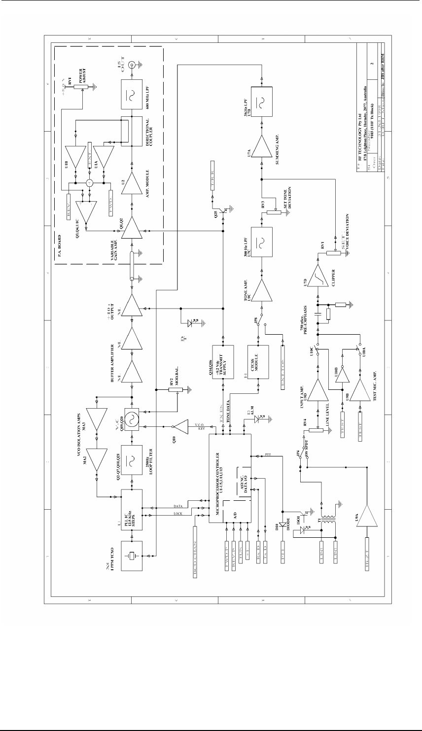
A.1 Block Diagram
Figure 1 shows the block signal flow diagram.
A.2 Circuit Diagrams
Figure 2 shows the detailed circuit diagram with component numbers and values for the
main (exciter) PCB. Figure 3 shows the detailed circuit diagram with component
numbers and values for the higher-power PA variation. Figure 4 shows the detailed
circuit diagram with component numbers and values for the lower-power PA variation.

RF
Technology T350/T500
Page 25
A ENGINEERING DIAGRAMS
A.3 Component Overlay Diagrams
Figure 5 shows the PCB overlay guide with component positions for the main (exciter)
PCB. Figure 6 shows the detailed circuit diagram with component numbers and values
for the higher-power PA variation. Figure 7 shows the detailed circuit diagram with
component numbers and values for the lower power PA variation.
Page 26 RF
Technology T350/T500
A ENGINEERING DIAGRAMS_________________
A.3 Component Overlay Diagrams
Figure 1: The block circuit diagram
RF
Technology T350/T500
Page 27
A.3 Component Overlay Diagrams________
_ A ENGINEERING DIAGRAMS
Figure 2
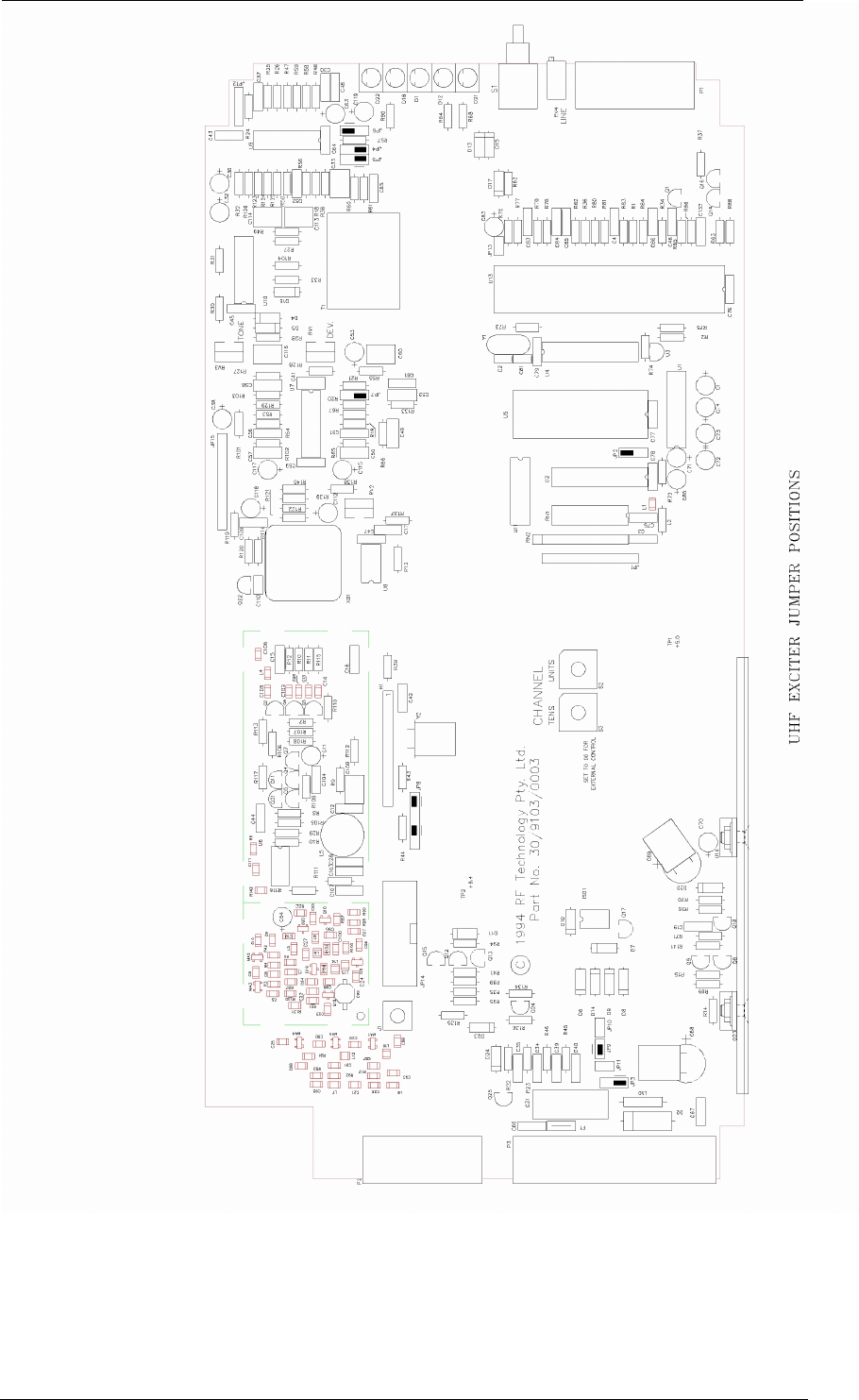
: The main board component overlay diagram.
Page 28 RF
Technology T350/T500
A ENGINEEERING DIAGRAMS
A.3 Component Overlay Diagrams
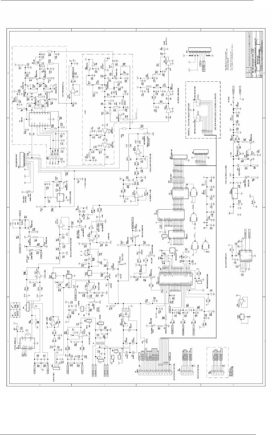
Figure 3: The component circuit diagram of the 9103 UHF Transmitter.

RF
Technology T350/T500
Page 29
This Page Is Blank Intentionally
Page 30 RF
Technology T350/T500
A ENGINEEERING DIAGRAMS
A.3 Component Overlay Diagrams
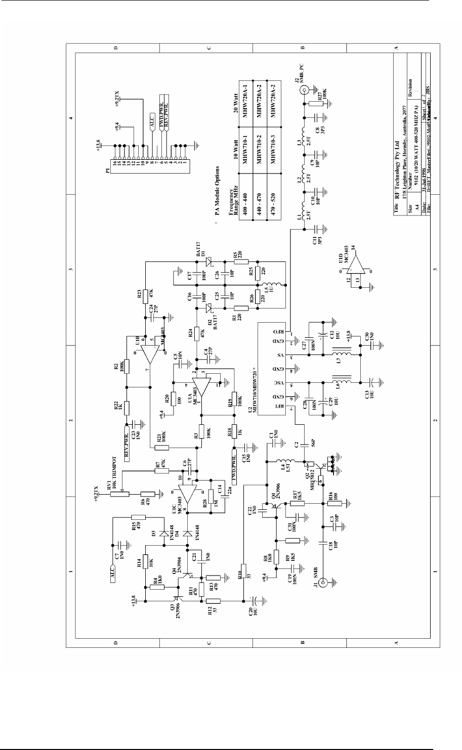
Figure 4: The component circuit diagram of the 9102 UHF PA.
RF
Technology T350/T500
Page 31
A.3 Component Overlay Diagrams A ENGINEERING DIAGRAMS
Figure 5: The component circuit diagram of the 9128/9149 UHF PA.
Page 32 RF
Technology T350/T500
A ENGINEERING DIAGRAMS
A.3 Component Overlay Diagrams
Figure 6
: The component overlay diagram for the higher-power PA board.
RF
Technology T350/T500
Page 33
A.3 Component Overlay Diagrams A ENGINEERING DIAGRAMS
Figure 7
: The component overlay diagram for the lower-power PA board

Page 34 RF
Technology T350/T500
B PARTS LIST T350/T500 Parts List
B T350/T500 Parts List (for PCB-30/9103/xxxx)
Main PCB Assembly Parts
Ref. Description Part Number
C1 Capacitor 10U 35V Rad Electro 41/2001/010U
C2 Capacitor 18P 2% 100V NPO Rad.1 45/2680/018P
C3 Capacitor 100N 10% 50V X7R Rad.2 46/2001/100N
C4 Capacitor 10N 10% 50V X7R Rad.2 46/2001/010N
C5 Capacitor 1N0 5% 63V NPO SM1206 46/3300/01N0
C6 Capacitor 1N0 5% 63V NPO SM1206 46/3300/01N0
C7 Capacitor 1N0 5% 63V NPO SM1206 46/3300/01N0
C8 Capacitor 1N0 5% 63V NPO SM1206 46/3300/01N0
C9 Capacitor 1N0 5% 63V NPO SM1206 46/3300/01N0
C10 Capacitor 1N0 5% 63V NPO SM1206 46/3300/01N0
C11 Capacitor 10U 35V Rad Electro 41/2001/010U
C12 Capacitor 47N 20% 50V X7R Rad.2 46/2001/047N
C13 Capacitor 1N0 5% 63V NPO SM1206 46/3300/01N0
C14 Capacitor 1N0 5% 63V NPO SM1206 46/3300/01N0
C15 Capacitor 10N 10% 50V X7R Rad.2 46/2001/010N
C16 Capacitor 10N 10% 50V X7R Rad.2 46/2001/010N
C17 Capacitor 10N 10% 50V X7R Rad.2 46/2001/010N
C18 Capacitor 1N0 5% 63V NPO SM1206 46/3300/01N0
C19 Capacitor 100N 10% 50V X7R Rad.2 46/2001/100N
C20 Capacitor 1N0 5% 63V NPO SM1206 46/3300/01N0
C21 Capacitor 100N 10% 63V X7R 1206 46/3310/100N
C22 Capacitor 3P3 5% 63V NPO SM1206 46/3300/03P3
C23 Capacitor 1N0 5% 63V NPO SM1206 46/3300/01N0
C24 Capacitor 2P7 5% 63V NP0 SM1206 46/3300/02P7
C25 Capacitor 1N0 5% 63V NPO SM1206 46/3300/01N0
C26 Capacitor, 6.8U SMD Tantalum 42/3009/06U8
C27 Capacitor 1N0 5% 63V NPO SM1206 46/3300/01N0
C28 Capacitor 1N0 5% 100V NPO Rad.2 46/2000/01N0
C29 Capacitor 1N0 5% 63V NPO SM1206 46/3300/01N0
C30 Capacitor 100N 10% 50V X7R Rad.2 46/2001/100N
C31 Capacitor 2U2 10% 100V MKT Rad.2 47/2010/02U2
C32 Capacitor 10U 35V Rad Electro 41/2001/010U
C33 Capacitor 1UO 10% 63V MKT Rad.2 47/2007/01U0
C34 Capacitor 1N0 5% 100V NPO Rad.2 46/2000/01N0
C35 Capacitor 1N0 5% 100V NPO Rad.2 46/2000/01N0
C36 Capacitor 10U 35V Rad Electro 41/2001/010U
C37 Capacitor 1N0 5% 100V NPO Rad.2 46/2000/01N0
C38 Capacitor 10U 35V Rad Electro 41/2001/010U
C39 Capacitor 1N0 5% 100V NPO Rad.2 46/2000/01N0
C40 Capacitor 1N0 5% 100V NPO Rad.2 46/2000/01N0
C41 Capacitor 100N 5% 50V MKT Rad.2 47/2007/100N
C42 Capacitor 100N 10% 50V X7R Rad.2 46/2001/100N
C43 Capacitor 1N0 5% 100V NPO Rad.2 46/2000/01N0
C44 Capacitor 10N 10% 50V X7R Rad.2 46/2001/010N
C45 Capacitor 1N0 5% 100V NPO Rad.2 46/2000/01N0
C46 Capacitor 10N 10% 50V X7R Rad.2 46/2001/010N
C47s Capacitor 1N0 5% 63V NPO SM1206 46/3300/01N0
C48 Capacitor 100N 10% 50V X7R Rad.2 46/2001/100N
C49 Capacitor 22N 5% 63V MKT Rad.2 47/2010/022N
C50 Capacitor 100N 5% 50V MKT Rad.2 47/2007/100N
C51 Capacitor 1N2 5% NPO Rad.2 46/2000/01N2
C52 Capacitor 1N5 10% 50V COG Rad.2 46/2000/01N5
C53 Capacitor 1U 35V Rad Electro 41/2001/001U
C54 Capacitor 10U 35V Rad Electro 41/2001/010U
C55 Capacitor 10N 10% 63V X7R SM1206 46/3310/010N

RF
Technology T350/T500
Page 35
B T350/T500 PARTS LIST
Ref. Description Part Number
C56 Capacitor 1N2 5% NPO Rad.2 46/2000/01N2
C57 Capacitor 100N 5% 50V MKT Rad.2 47/2007/100N
C58 Capacitor 22N 5% 63V MKT Rad.2 47/2010/022N
C59s Capacitor 1N0 5% 63V NPO SM1206 46/3300/01N0
C60 Capacitor 1UO 10% 63V MKT Rad.2 47/2007/01U0
C61 Capacitor 100N 10% 50V X7R Rad.2 46/2001/100N
C62 Capacitor 100N 10% 50V X7R Rad.2 46/2001/100N
C63 Capacitor 10U 35V Rad Electro 41/2001/010U
C64s Capacitor 1N0 5% 63V NPO SM1206 46/3300/01N0
C65 Capacitor 1N0 5% 100V NPO Rad.2 46/2000/01N0
C66 Capacitor 100N 10% 50V X7R Rad.2 46/2001/100N
C67 Capacitor 100N 10% 50V X7R Rad.2 46/2001/100N
C68 Capacitor 470U 25V RB Electro 41/2001/470U
C69 Capacitor 470U 25V RB Electro 41/2001/470U
C70 Capacitor 10U 35V Rad Electro 41/2001/010U
C71 Capacitor 10U 35V Rad Electro 41/2001/010U
C72 Capacitor 10U 35V Rad Electro 41/2001/010U
C73 Capacitor 10U 35V Rad Electro 41/2001/010U
C74 Capacitor 10U 35V Rad Electro 41/2001/010U
C75 Capacitor 1N0 5% 100V NPO Rad.2 46/2000/01N0
C76 Capacitor 1N0 5% 100V NPO Rad.2 46/2000/01N0
C77 Capacitor 100N 10% 50V X7R Rad.2 46/2001/100N
C78 Capacitor 100N 10% 50V X7R Rad.2 46/2001/100N
C79 Capacitor 100N 10% 50V X7R Rad.2 46/2001/100N
C80 Capacitor 10U 35V Rad Electro 41/2001/010U
C81 Capacitor 18P 2% 100V NPO Rad.1 45/2680/018P
C82 Capacitor 10U 35V Rad Electro 41/2001/010U
C83 Capacitor 10N 10% 50V X7R Rad.2 46/2001/010N
C84 Capacitor 10N 10% 50V X7R Rad.2 46/2001/010N
C85 Capacitor 10N 10% 50V X7R Rad.2 46/2001/010N
C86 Capacitor 10N 10% 50V X7R Rad.2 46/2001/010N
C87 Capacitor 100N 10% 63V X7R 1206 46/3310/100N
C88 Capacitor 10P 5% 63V NPO SM1206 46/3300/010P
C89 Capacitor 100N 10% 63V X7R 1206 46/3310/100N
C90 Capacitor 10P 5% 63V NPO SM1206 46/3300/010P
C91 Capacitor 100N 10% 63V X7R 1206 46/3310/100N
C92 Capacitor 1N0 5% 63V NPO SM1206 46/3300/01N0
C93 Capacitor 100N 10% 63V X7R 1206 46/3310/100N
C94 Capacitor 1P8 5% 63V NPO SM1206 46/3300/01P8
C95 Capacitor 100N 10% 63V X7R 1206 46/3310/100N
C96 Capacitor 1N0 5% 63V NPO SM1206 46/3300/01N0
C97 Capacitor 1N0 5% 63V NPO SM1206 46/3300/01N0
C98 Capacitor 1P8 5% 63V NPO SM1206 46/3300/01P8
C99 Capacitor Trim 5-25P 49/3002/025P
C100 Capacitor 1N0 5% 63V NPO SM1206 46/3300/01N0
C101 Capacitor 1N0 5% 63V NPO SM1206 46/3300/01N0
C102 Capacitor 10N 10% 63V X7R 1206 46/3310/010N
C103 Capacitor 47N 20% 50V X7R Rad.2 46/2001/047N
C104 Capacitor 100N 10% 50V X7R Rad.2 46/2001/100N
C105 Capacitor 1N0 5% 63V NPO SM1206 46/3300/01N0
C106 Capacitor 100N 10% 63V X7R 1206 46/3310/100N
C107 Capacitor 47N 20% 50V X7R Rad.2 46/2001/047N
C108 Capacitor 1UO 10% 63V MKT Rad.2 47/2007/01U0
C109 Capacitor 10N 10% 50V X7R Rad.2 46/2001/010N
C110 Capacitor 47P 2% 100V NPO Rad.1 45/2680/047P
C111 Capacitor 100N 10% 63V X7R 1206 46/3310/100N
C112 Capacitor 100U 25V RB Electro 41/1025/100U
C113 Capacitor 1UO 10% 63V MKT Rad.2 47/2007/01U0

Page 36 RF
Technology T350/T500
B T350/T500 PARTS LIST
Ref. Description Part Number
C114 Capacitor 1UO 10% 63V MKT Rad.2 47/2007/01U0
C115 Capacitor 100U 25V RB Electro 41/1025/100U
C116 Capacitor 1UO 10% 63V MKT Rad.2 47/2007/01U0
C117 Capacitor 100U 25V RB Electro 41/1025/100U
C118 Capacitor 10U 35V Rad Electro 41/2001/010U
C119 Capacitor 10U 35V Rad Electro 41/2001/010U
C132 Capacitor 10N 10% 50V X7R Rad.2 46/2001/010N
D1 Diode LED Red T1 3/4 21/1010/LEDR
D2 Diode 3Amplifier 1KV Rectifier 21/1080/5408
D3 Diode VCapacitor MMBV105G SOT23 21/3060/105G
D4 Diode Silicon 1N4148 21/1010/4148
D5 Diode Silicon 1N4148 21/1010/4148
D6 Diode Silicon GP 21/1010/4002
D7 Diode Zen 1N4751 30V 1W AXIAL 21/1040/4751
D8 Diode Silicon GP 21/1010/4002
D9 Diode Silicon GP 21/1010/4002
D10 Diode Silicon 1N4148 21/1010/4148
D11 Diode Silicon 1N4148 21/1010/4148
D12 Diode LED Yellow T1 3/4 21/1010/LEDY
D13 Diode Silicon 1N4148 21/1010/4148
D14 Diode Silicon GP 21/1010/4002
D15 Diode Silicon 1N4148 21/1010/4148
D16 Diode Silicon 1N4148 21/1010/4148
D17 Diode Silicon 1N4148 21/1010/4148
D18 Diode LED Green T1 3/4 21/1010/LEDG
D19 Diode Schottkey BAT17 SOT23 21/3030/0017
D20 Diode 8V2 Zener 21/1040/B8V2
D21 Diode LED Green T1 3/4 21/1010/LEDG
D22 Diode LED Green T1 3/4 21/1010/LEDG
D23 Diode Silicon 1N4148 21/1010/4148
D24 Diode Zen 1N4751 30V 1W AXIAL 21/1040/4751
D25(L9) SMD Diode, 100ma 50v 21/3009/AS85
H1 Hybred CTCSS 13/9150/0002
ISO1 IC Opto-Isolator 4N33 25/1010/4N33
J1 Connector Coax SKT SMB Vertical PCB 35/2004/0001
JP2 Connector 3Way Header 35/2501/0003
JP3 Connector 3Way Header 35/2501/0003
JP4 Connector 3Way Header 35/2501/0003
JP5 Connector 3Way Header 35/2501/0003
JP6 Connector 3Way Header 35/2501/0003
JP7 Connector 3Way Header 35/2501/0003
JP8 Connector 6Way Header 35/2501/0006
JP9 Connector 2Way Header 35/2501/0002
JP10 Connector 2Way Header 35/2501/0002
JP11 Connector 2Way Header 35/2501/0002
JP13 Connector 2Way Header 35/2501/0002
JP14 Connector 16Way Shr'd Header 35/2502/0016
JP15 Connector 10Way Header 35/2501/0010
L1 Ferrite Bead SMD 37/3321/LM31
L2 Inductor 1uH Axial 37/2021/001U
L3 Ferrite Bead SMD 37/3321/LM31
L4 Ferrite Bead SMD 37/3321/LM31
L5 Inductor 150mH 10RBH 37/2021/1RBH
L6 Inductor 220N 10% Choke SM1206 37/3320/220N
L7 Ferrite Bead SMD 37/3321/LM31
L8 Ferrite Bead SMD 37/3321/LM31
L10 Inductor 6 Hole Ferrite RFC 37/1021/0001
L11 Inductor 220N 10% Choke SM1206 37/3320/220N
L12 Inductor 220N 10% Choke SM1206 37/3320/220N
L13 Inductor 220N 10% Choke SM1206 37/3320/220N

RF
Technology T350/T500
Page 37
B T350/T500 PARTS LIST
Ref. Description Part Number
L14 Inductor 220N 10% Choke SM1206 37/3320/220N
MA1 Amplifier MMIC MWA0311L SOT143 24/3010/0311
MA2 Amplifier MMIC MWA0311L SOT143 24/3010/0311
MA3 Amplifier MMIC MWA0311L SOT143 24/3010/0311
MA4 Amplifier MMIC VAM-6 SOT143 24/3010/VAM6
MA5 Amplifier MMIC MWA0311L SOT143 24/3010/0311
P1 Filter D RT AGL 9W F Ferrite 35/5012/009F
P3 Filter D RT AGL 25W M Ferrite 35/5012/025M
Q1 Transistor GP NPN MMBT3904 SOT23 27/3020/3904
Q2 Transistor GP NPN MMBT3904 SOT23 27/3020/3904
Q3 Transistor GP PNP MMBT3906 SOT23 27/3010/3906
Q4 Fast Switching SMD Transistor 27/3010/5771
Q5 Transistor GP NPN MMBT3904 SOT23 27/3020/3904
Q6 Transistor GP NPN MMBT3904 SOT23 27/3020/3904
Q7 Transistor GP PNP MMBT3906 SOT23 27/3010/3906
Q8 Transistor GP NPN MMBT3904 SOT23 27/3020/3904
Q9 SMD FET NJ MMBF5459LT1 SOT23 27/3020/5459
Q10 Transistor GP NPN MMBT2369 SOT23 27/3020/2369
Q11 Transistor GP NPN MMBT2369 SOT23 27/3010/2369
Q12 Transistor GP PNP MMBT3906 SOT23 27/3010/3906
Q13 Transistor GP NPN MMBT3904 SOT23 27/3020/3904
Q14 Transistor GP NPN MMBT3904 SOT23 27/3020/3904
Q15 Transistor GP NPN MMBT3904 SOT23 27/3020/3904
Q16 Transistor GP PNP MMBT3906 SOT23 27/3010/3906
Q17 SMD FET NJ MMBF5459LT1 SOT23 27/3020/5459
Q18 Transistor GP NPN MMBT3904 SOT23 27/3020/3904
Q19 FET NJ MMBFJ309 SOT23 27/3030/J309
Q20 Transistor GP NPN MMBT3904 SOT23 27/3020/3904
Q21 Fast Switching SMD Transistor 27/3010/5771
Q22 Transistor GP NPN MMBT2369 SOT23 27/3020/2369
Q23 Transistor PNP MJF6107 TO22O 27/2010/6107
Q24 Transistor GP PNP MMBT3906 SOT23 27/3010/3906
Q25 Transistor NPN GP MPSA06 TO92 27/2010/PA06
R1 Resistor 5K11 1% 0.25W Axial 51/1010/5K11
R2 Resistor 4K7 5% 0.25W Axial 51/1040/04K7
R3 Resistor 100 5% 0.25W SM1206 51/3380/0100
R4 Resistor 100 5% 0.25W SM1206 51/3380/0100
R5 Resistor 100 5% 0.25W SM1206 51/3380/0100
R6 Resistor 15R 5% 0.25W SM1206 51/3380/0015
R7 Resistor 68 5% 0.25W Axial 51/1040/0068
R8 Resistor 3K3 5% 0.25W Axial 51/1040/03K3
R9 Resistor 1K0 5% 0.25W Axial 51/1040/01K0
R10 Resistor 1K0 5% 0.25W Axial 51/1040/01K0
R11 Resistor 1K0 5% 0.25W Axial 51/1040/01K0
R12 Resistor 1K0 5% 0.25W Axial 51/1040/01K0
R13 Resistor 1K0 5% 0.25W Axial 51/1040/01K0
R14 Resistor 680 5% 0.25W Axial 51/1040/0680
R15 Resistor 6K8 5% 0.25W Axial 51/1040/06K8
R16 Resistor 680 5% 0.25W Axial 51/1040/0680
R17 Resistor 270 5% 0.25W SM1206 51/3380/0270
R18 Resistor 10K 5% 0.25W Axial 51/1040/010K
R19 Resistor 47K 5% 0.25W Axial 51/1040/047K
R20 Resistor 1M0 5% 0.25W Axial 51/1040/01M0
R21 Resistor 10K 5% 0.25W Axial 51/1040/010K
R22 Resistor 10K 5% 0.25W Axial 51/1040/010K
R23 Resistor 10K 5% 0.25W Axial 51/1040/010K
R24 Resistor 330 5% 0.25W Axial 51/1040/0330
R25 Resistor 330 5% 0.25W Axial 51/1040/0330
R26 Resistor 18K 5% 0.25W Axial 51/1040/018K
R27 Resistor 10K0 1% 0.25W Axial 51/1010/010K

Page 38 RF
Technology T350/T500
B T350/T500 PARTS LIST
Ref. Description Part Number
R28 Resistor 10K 5% 0.25W Axial 51/1040/010K
R29 Resistor 2K2 5% 0.25W Axial 51/1040/02K2
R30 Resistor 470K 5% 0.25W Axial 51/1040/470K
R31 Resistor 10K 5% 0.25W Axial 51/1040/010K
R32 Resistor 10K 5% 0.25W Axial 51/1040/010K
R33 Resistor 10K 5% 0.25W Axial 51/1040/010K
R34 Resistor 100K 5% 0.25W Axial 51/1040/100K
R35 Resistor 100K 5% 0.25W Axial 51/1040/100K
R36 Resistor 5K11 1% 0.25W Axial 51/1010/5K11
R37 Resistor 10K 5% 0.25W Axial 51/1040/010K
R38 Resistor 91K 5% 0.25W Axial 51/1040/091K
R39 Resistor 22 5% 0.25W Axial 51/1040/0022
R40 Resistor 4K7 5% 0.25W Axial 51/1040/04K7
R41 Resistor 2K2 5% 0.25W Axial 51/1040/02K2
R42 Resistor 100 5% 0.25W SM1206 51/3380/0100
R43 Resistor 100K 5% 0.25W Axial 51/1040/100K
R44 Resistor 6K8 5% 0.25W Axial 51/1040/06K8
R45 Resistor 10K 5% 0.25W Axial 51/1040/010K
R46 Resistor 10K 5% 0.25W Axial 51/1040/010K
R47 Resistor 64K9 1% 0.25W Axial 51/1010/64K9
R48 Resistor 64K9 1% 0.25W Axial 51/1010/64K9
R49 Resistor 7K50 1% 0.25W Axial 51/1010/07K5
R50 Resistor 1M0 5% 0.25W Axial 51/1040/01M0
R51 Resistor 10K 5% 0.25W SM1206 51/3380/010K
R52 Resistor 10K 5% 0.25W SM1206 51/3380/010K
R53 Resistor 7K50 1% 0.25W Axial 51/1010/07K5
R54 Resistor 10K0 1% 0.25W Axial 51/1010/010K
R55 Resistor 91K 5% 0.25W Axial 51/1040/091K
R56 Resistor 100K 5% 0.25W Axial 51/1040/100K
R57 Resistor 91K 5% 0.25W Axial 51/1040/091K
R58 Resistor 64K9 1% 0.25W Axial 51/1010/64K9
R59 Resistor 64K9 1% 0.25W Axial 51/1010/64K9
R60 Resistor 1K2 5% 0.25W Axial 51/1040/01K2
R61 Resistor 1K2 5% 0.25W Axial 51/1040/01K2
R62 Resistor 10K 5% 0.25W Axial 51/1040/010K
R63 Resistor 4K7 5% 0.25W Axial 51/1040/04K7
R64 Resistor 390 5% 0.25W Axial 51/1040/0390
R65 Resistor 47K 5% 0.25W Axial 51/1040/047K
R66 Resistor 47K 5% 0.25W Axial 51/1040/047K
R67 Resistor 10K 5% 0.25W Axial 51/1040/010K
R68 Resistor 680 5% 0.25W Axial 51/1040/0680
R69 Resistor 1K 5% 0.25W Axial 51/1040/01K0
R70 Resistor 680 5% 0.25W Axial 51/1040/0680
R71 Resistor 4K7 5% 0.25W Axial 51/1040/04K7
R72 Resistor 47 5% 0.25W Axial 51/1040/0047
R73 Resistor 10M 5% 0.25W Axial 51/1040/010M
R74 Resistor 4K7 5% 0.25W Axial 51/1040/04K7
R75 Resistor 4K7 5% 0.25W Axial 51/1040/04K7
R76 Resistor 10K 5% 0.25W Axial 51/1040/010K
R77 Resistor 1K0 5% 0.25W Axial 51/1040/01K0
R78 Resistor 6K49 1% 0.25W Axial 51/1010/6K49
R79 Resistor 28K7 1% 0.25W Axial 51/1010/28K7
R80 Resistor 5K11 1% 0.25W Axial 51/1010/5K11
R81 Resistor 5K11 1% 0.25W Axial 51/1010/5K11
R82 Resistor 5K11 1% 0.25W Axial 51/1010/5K11
R83 Resistor 5K11 1% 0.25W Axial 51/1010/5K11
R84 Resistor 100K 5% 0.25W Axial 51/1040/100K
R85 Resistor 2K2 5% 0.25W Axial 51/1040/02K2
R86 Resistor 680 5% 0.25W Axial 51/1040/0680

RF
Technology T350/T500
Page 39
B T350/T500 PARTS LIST
Ref. Description Part Number
R87 Resistor 2K2 5% 0.25W SM1206 51/3380/02K2
R88 Resistor 1K0 5% 0.25W Axial 51/1040/01K0
R89 Resistor 10K 5% 0.25W Axial 51/1040/010K
R90 Resistor 180 5% 0.25W Axial 51/1040/0180
R91 Resistor 100 5% 0.25W SM1206 51/3380/0100
R92 Resistor 180 5% 0.25W SM1206 51/3380/0180
R93 Resistor 270R 5% 0.25W SM1206 51/3380/0270
R94 Resistor 1K8 5% 0.25W Axial 51/1040/01K8
R95 Resistor 1K0 5% 0.25W Axial 51/1040/01K0
R96 Resistor 15R 5% 0.25W SM1206 51/3380/0015
R97 Resistor 470R 5% 0.25W SM1206 51/3380/0470
R98 Resistor 47R 5% 0.25W SM1206 51/3380/0047
R99 Resistor 10K 5% 0.25W SM1206 51/3380/010K
R100 Resistor 47R 5% 0.25W SM1206 51/3380/0047
R101 Resistor 4K32 1% 0.25W Axial 51/1010/4K32
R102 Resistor 4K32 1% 0.25W Axial 51/1010/4K32
R103 Resistor 4K32 1% 0.25W Axial 51/1010/4K32
R104 Resistor 470K 5% 0.25W Axial 51/1040/470K
R105 Resistor 1K0 5% 0.25W Axial 51/1040/01K0
R106 Resistor 560 5% 0.25W Axial 51/1040/0560
R107 Resistor 3K3 5% 0.25W Axial 51/1040/03K3
R108 Resistor 560 5% 0.25W Axial 51/1040/0560
R109 Resistor 1K0 5% 0.25W Axial 51/1040/01K0
R110 Resistor 100 5% 0.25W Axial 51/1040/0100
R111 Resistor 2K2 5% 0.25W Axial 51/1040/02K2
R112 Resistor 220K 5% 0.25W Axial 51/1040/220K
R113 Resistor 68 5% 0.25W Axial 51/1040/0068
R114 Resistor 47K 5% 0.25W Axial 51/1040/047K
R115 Resistor 1K0 5% 0.25W Axial 51/1040/01K0
R116 Resistor 10K 5% 0.25W Axial 51/1040/010K
R117 Resistor 1K0 5% 0.25W Axial 51/1040/01K0
R119 Resistor 22 5% O.25W Axial 51/1040/0022
R120 Resistor 220 5% 0.25W Axial 51/1040/0220
R121 Resistor 120K 5% 0.25W Axial 51/1040/120K
R123 Resistor 150K 5% 0.25W Axial 51/1040/150K
R124 Resistor 150K 5% 0.25W Axial 51/1040/150K
R125 Resistor 680K 5% 0.25W Axial 51/1040/680K
R126 Resistor 680K 5% 0.25W Axial 51/1040/680K
R127 Resistor 470K 5% 0.25W Axial 51/1040/470K
R128 Resistor 560K 5% 0.25W Axial 51/1040/560K
R129 Resistor 470K 5% 0.25W Axial 51/1040/470K
R130 Resistor 470 5% 0.25W SM1206 51/3380/0470
R131 Resistor 47R 5% 0.25W SM1206 51/3380/0047
R132 Resistor 47R 5% 0.25W SM1206 51/3380/0047
R133 Resistor 510K 5% 0.25W Axial 51/1040/510K
R134 Resistor 270 5% 0.25W Axial 51/1040/0270
R135 Resistor 470 5% 0.25W Axial 51/1040/0470
R136 Resistor 1K0 5% 0.25W Axial 51/1040/01K0
R137 Resistor 10K 5% 0.25W Axial 51/1040/010K
R138 Resistor 22K 5% 0.25W Axial 51/1040/022K
R139 Resistor 4K7 5% 0.25W Axial 51/1040/04K7
R140 Resistor 100K 5% 0.25W Axial 51/1040/100K
R141 Resistor 10R 5% 0.25W Axial 51/1040/0010
R142 Resistor 470K 5% 0.25W SM1206 51/3380/470K
RN1 Resistor Pack 100K X8 DIP16 52/2002/100K
RN2 Resistor Pack 10K SIP10 52/2002/010K
RV1 Trimpot 10K 1 Turn Vertical 53/1020/010K
RV2 Trimpot 10K 1 Turn Vertical 53/1020/010K
RV3 Trimpot 10K 1 Turn Vertical 53/1020/010K
RV4 Trimpot 10K Multi-turn Horizontal 53/2060/010K

Page 40 RF
Technology T350/T500
B T350/T500 PARTS LIST
Ref. Description Part Number
S1 Switch PSH BTN SPDT & Capacitor 31/0005/E121
T1 Transformer Line 600 Ohm 37/2040/5065
U1 IC RS232 Inter MAX232C 26/2001/232C
U2 IC 3 State BUF 74HC244N 26/2030/244N
U3 IC Micro Super MC34064P-5 26/2000/064P
U4 IC 8 Bit Latch 74HC573N 26/2030/C573
U5 IC EPROM 27C256 26/2090/C256
U6 IC Frequency SYN MB1501 SO16X 26/2000/1501
U7 IC Quad OP Amplifier TLC274 25/2050/274C
U8 IC Dual FET OP Amplifier DIP8 25/1050/272C
U9 IC Quad OP Amplifier TLC274 25/2050/274C
U10 IC Analogue Gate MC14066B 26/2040/4066
U11 IC Quad NAND 74C00 DIP14 26/2031/4C00
U13 IC Micro 68HC11A1P 26/2000/HC11
U14 IC Volt Regulator LM7805 25/2040/7805
XO1 TCXO 12.8 MHz O91/143-2 32/2030/12.8
Y1 Crystal 8.0 MHz 32/2049/08M0
Y2 Crystal 4.0 MHz 32/2049/04M0
Coaxial Resonator (CR1) Listing for T350 – T500
Model Part #
T350A 12/0001/T350
T350B 12/0001/T350
T350C 12/0001/T330
T500A 12/0001/T400
T500B 12/0001/T450
Power Amplifier Assembly (for PCB 30/9149)
These parts common to all Amplifiers on T350 / T500
Ref. Description Part Number
C1 Capacitor 1N0 5% 63V NPO SM1206 46/3300/01N0
C2 Capacitor 56P 5% 63V NPO SM1206 46/3300/056P
C4 Capacitor 27P 2% 100V NPO Rad.1 45/2680/027P
C5 Capacitor 10N 10% 50V X7R Rad.2 46/2001/010N
C6 Capacitor 27P 2% 100V NPO Rad.1 45/2680/027P
C7 Capacitor 1N0 5% 100V NPO Rad.2 46/2000/01N0
C12 Capacitor 10U 35V Rad Electro 41/2001/010U
C13 Capacitor 10U 35V Rad Electro 41/2001/010U
C14 Capacitor 22N 5% 63V MKT Rad.2 47/2010/022N
C15 Capacitor 1N0 5% 100V NPO Rad.2 46/2000/01N0
C16 Capacitor 100P 5% 63V NPO 1206 46/3300/100P
C17 Capacitor 100P 5% 63V NPO 1206 46/3300/100P
C18 Capacitor 1N0 5% 63V NPO SM1206 46/3300/01N0
C20 Capacitor 10U 35V Rad Electro 41/2001/010U
C21 Capacitor 27P 2% 100V NPO Rad.1 45/2680/027P
C23 Capacitor 1N0 5% 100V NPO Rad.2 46/2000/01N0
C24 Capacitor 27P 2% 100V NPO Rad.1 45/2680/027P
C25 Capacitor 10P 5% 63V NPO SM1206 46/3300/010P
C26 Capacitor 10P 5% 63V NPO SM1206 46/3300/010P

RF
Technology T350/T500
Page 41
B T350/T500 PARTS LIST
Ref. Description Part Number
C27 Capacitor 100N 10% 63V X7R 1206 46/3310/100N
C28 Capacitor 100N 10% 63V X7R 1206 46/3310/100N
C29 Capacitor 10U 35V Rad Electro 41/2001/010U
C30 Capacitor 1N0 5% 63V NPO SM1206 46/3300/01N0
C31 Capacitor 100N 10% 50V X7R Rad.2 46/2001/100N
C32 Capacitor 100N 10% 63V X7R 1206 46/3310/100N
C33 Capacitor 10U 35V Rad Electro 41/2001/010U
C34 Capacitor 1N0 5% 100V NPO Rad.2 46/2000/01N0
C35 Capacitor 22N 5% 63V MKT Rad.2 47/2010/022N
C36 Capacitor 27P 2% 100V NPO Rad.1 45/2680/027P
D1 Diode Schottkey BAT17 SOT23 21/3030/0017
D2 Diode Schottkey BAT17 SOT23 21/3030/0017
D3 Diode Silicon 1N4148 21/1010/4148
D4 Diode Silicon 1N4148 21/1010/4148
D5 Diode Silicon 1N4148 21/1010/4148
J2 Connector Coax SMB PCB Horizontal 35/2001/0001
L5 Inductor 1U0 10% Choke SM1008 37/3320/01U0
L6 Inductor 6 Hole Ferrite RFC 37/1021/0001
L7 Inductor 6 Hole Ferrite RFC 37/1021/0001
L8 Inductor 6 Hole Ferrite RFC 37/1021/0001
P1 Connector 16 Way Horizontal Shr'd Header 35/2503/0016
Q2 Transistor RF NPN MRF5812 SO8 27/3020/5812
Q3 Transistor GP PNP MPSW5 11A,A TO92 27/2010/PW51
Q4 Transistor GP NPN 2N3904 TO92 27/2020/3904
Q5 Transistor ZTX751 ZETEX TO92 27/2010/X751
Q6 Transistor GP NPN 2N3904 TO92 27/2020/3904
Q7 Transistor GP NPN 2N3904 TO92 27/2020/3904
R1 Resistor 220 5% 0.25W SM1206 51/3380/0220
R2 Resistor 100K 5% 0.25W Axial 51/1040/100K
R3 Resistor 100K 5% 0.25W Axial 51/1040/100K
R4 Resistor 100R 5% 0.25W Axial 51/1040/0100
R5 Resistor 220 5% 0.25W SM1206 51/3380/0220
R6 Resistor 15K 5% 0.25W Axial 51/1040/015K
R7 Resistor 100K 5% 0.25W Axial 51/1040/100K
R10 Resistor 4R7 5% 0.25W Axial 51/1040/04R7
R11 Resistor 1K 5% 0.25W Axial 51/1040/01K0
R12 Resistor 22 5% 0.25W Axial 51/1040/0022
R13 Resistor 470 5% 0.25W Axial 51/1040/0470
R14 Resistor 10K 5% 0.25W Axial 51/1040/010K
R15 Resistor 470 5% 0.25W Axial 51/1040/0470
R16 Resistor 470 5% 0.25W SM1206 51/3380/0470
R17 Resistor 5K6 5% 0.25W Axial 51/1040/05K6
R18 Resistor 1K0 5% 0.25W Axial 51/1040/01K0
R19 Resistor 100K 5% 0.25W Axial 51/1040/100K
R20 Resistor 100 5% 0.25W Axial 51/1040/0100
R21 Resistor 47K 5% 0.25W Axial 51/1040/047K
R22 Resistor 1K0 5% 0.25W Axial 51/1040/01K0
R23 Resistor 47K 5% 0.25W SM1206 51/3380/047K
R24 Resistor 47K 5% 0.25W SM1206 51/3380/047K
R25 Resistor 220R 5% 0.25W SM1206 51/3380/0220
R26 Resistor 220R 5% 0.25W SM1206 51/3380/0220
R27 Resistor 100K 5% 0.25W Axial 51/1040/100K
R28 Resistor 1M0 5% 0.25W Axial 51/1040/01M0
R29 Resistor 4K7 5% 0.25W Axial 51/1040/04K7
R30 Resistor 10K 5% 0.25W Axial 51/1040/010K
R31 Resistor 680R 5% 0.25W Axial 51/1040/0680
R32 Resistor 10K 5% 0.25W Axial 51/1040/010K
R33 Resistor 10K 5% 0.25W Axial 51/1040/010K
R34 Resistor 4K7 5% 0.25W Axial 51/1040/04K7
R35 Resistor 1M0 5% 0.25W Axial 51/1040/01M0

Page 42 RF
Technology T350/T500
B T350/T500 PARTS LIST
Ref. Description Part Number
R36 Resistor 47K 5% 0.25W Axial 51/1040/047K
R37 Resistor 15K 5% 0.25W Axial 51/1040/015K
R38 Resistor 4R7 5% 0.25W Axial 51/1040/04R7
R39 Capacitor 2P2 5% 63V NPO 1206 46/3300/02P2
RV1 Trimpot 10K 1 Turn Vertical 53/1020/010K
RV2 Trimpot 10K 1 Turn Vertical 53/1020/010K
U1 IC Quad OP Amplifier MC3403P 25/1050/3403
Additional parts for Amplifiers in all T350’s
Ref. Description Part Number
L1 Inductor Moulded 3.5 Turn 37/2021/0003
L2 Inductor Moulded 3.5 Turn 37/2021/0003
L3 Inductor Moulded 3.5 Turn 37/2021/0003
L4 Inductor Moulded 3.5 Turn 37/2021/0003
C3 Capacitor 10P 5% 63V NPO SM1206 46/3300/010P
C8 Capacitor 4P5 5% 250V Silver Mica 48/3003/04P5
C9 Capacitor 13P 5% 250V Silver Mica 48/3003/013P
C10* Capacitor 13P 5% 250V MC Mica 48/3002/013P
C11 Capacitor 4P5 5% 250V Silver Mica 48/3003/04P5
C37 Capacitor 22P 5% 63V NPO SM1206 46/3300/022P
*C10 is omitted from T350D
Additional parts for Amplifiers in all T500’s
Ref. Description Part Number
L1 Inductor Moulded 2.5 Turn 37/2021/0002
L2 Inductor Moulded 2.5 Turn 37/2021/0002
L3 Inductor Moulded 2.5 Turn 37/2021/0002
L4 Inductor Moulded 1.5 Turn 37/2021/0001
C3 Capacitor 4P7 5% 63V NPO SM1206 46/3300/04P7
C8 Capacitor 3P 5% 250V Silver Mica 48/3003/003P
C9 Capacitor 10P 5% 250V Silver Mica 48/3003/010P
C10 Capacitor 10P 5% 250V MC Mica 48/3002/010P
C11 Capacitor 3P 5% 250V Silver Mica 48/3003/003P
C37 Capacitor 6P8 5% 63V NPO SM1206 46/3300/06P8
RF Power Module Listing for all Amplifiers
Model Frequency RF Power Module
T350A 360 – 380 MHz 18/M577/29SL
T350B 375 – 400 MHz 18/M577/29UL
T350C 330 – 365 MHz 18/M577/29EL
T350D 300 – 330 MHz 18/M577/29GL
T500A 400 – 430 MHz 18/M577/088L
T500B 430 – 500 MHz 18/M577/88UH
T500B 465 – 510 MHz 18/M577/88SH