RIFO TECHNOLOGY RIFO BLE Module User Manual Manual
RIFO TECHNOLOGY CO., LTD. BLE Module Manual
Manual
____________________________________________________________________________________
2.4-GHz Bluetooth® low energy System-on-Module
Model : 2.4GHz RF Module
Part No : TM41B1412-xxxx
Version : V3.3
Date : 2015.07.23
TM41B1412-Fxxx
2
■ Applications
■ Selection Guide
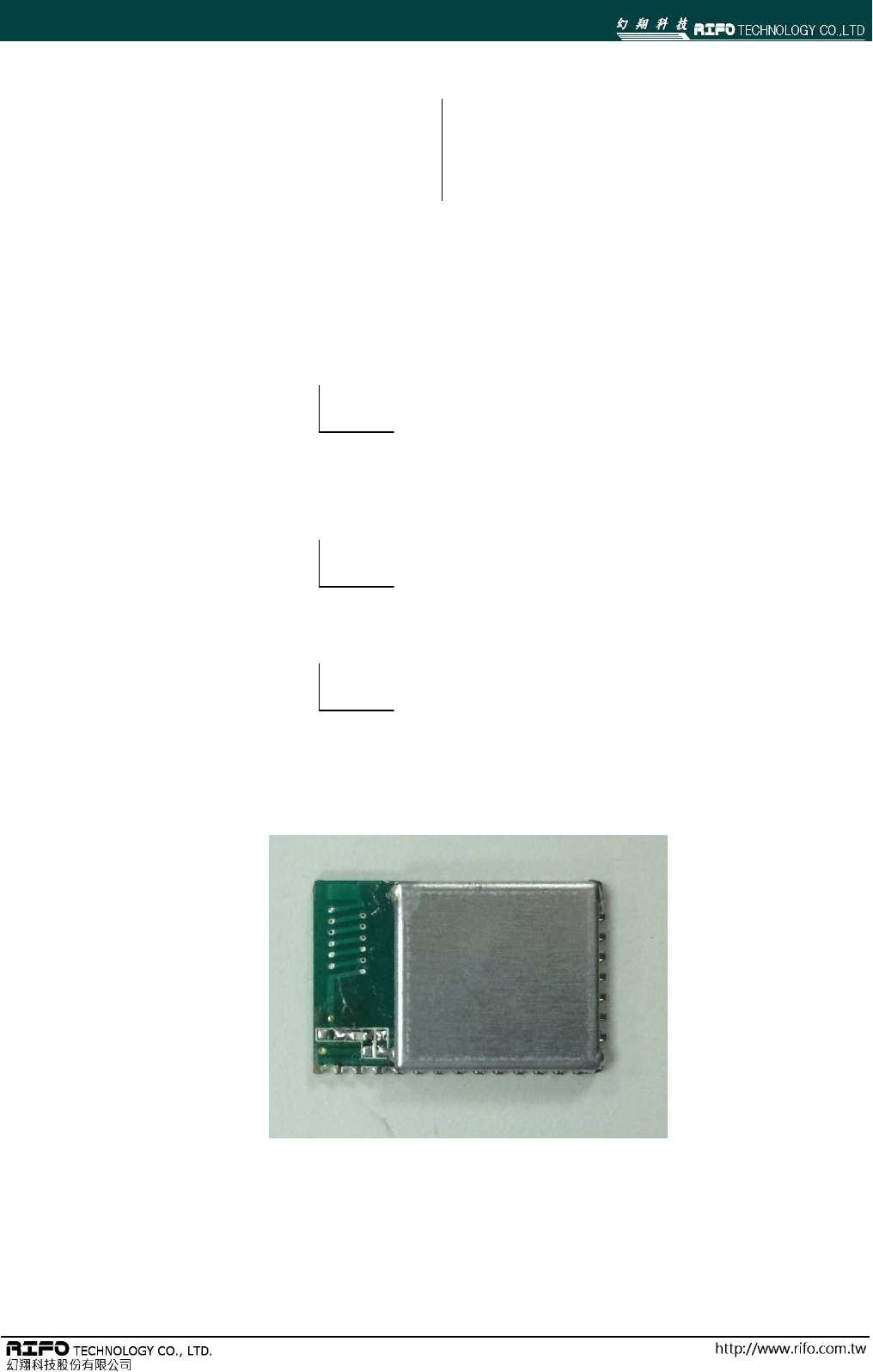
Denomination :2.4GHz Bluetooth RF Module
Part No. :TM41B1412-SFxxx (with Shielding case)
128/256 KB in-system Programmable Flash
TM41B1412-Fxxx (without Shielding case)
128/256 KB in-system Programmable Flash
TM41B1412-Exxxx (External Antenna)
128/256 KB in-system Programmable Flash
˙2.4-GHz Bluetooth low energy Systems
˙Proprietary 2.4-GHz Systems
˙Human-Interface Devices (Keyboard, Mouse
,Remote Control)
˙Sports and Leisure Equipment
˙Mobile Phone Accessories
˙Consumer Electronics
TM41B1412-Fxxx
3
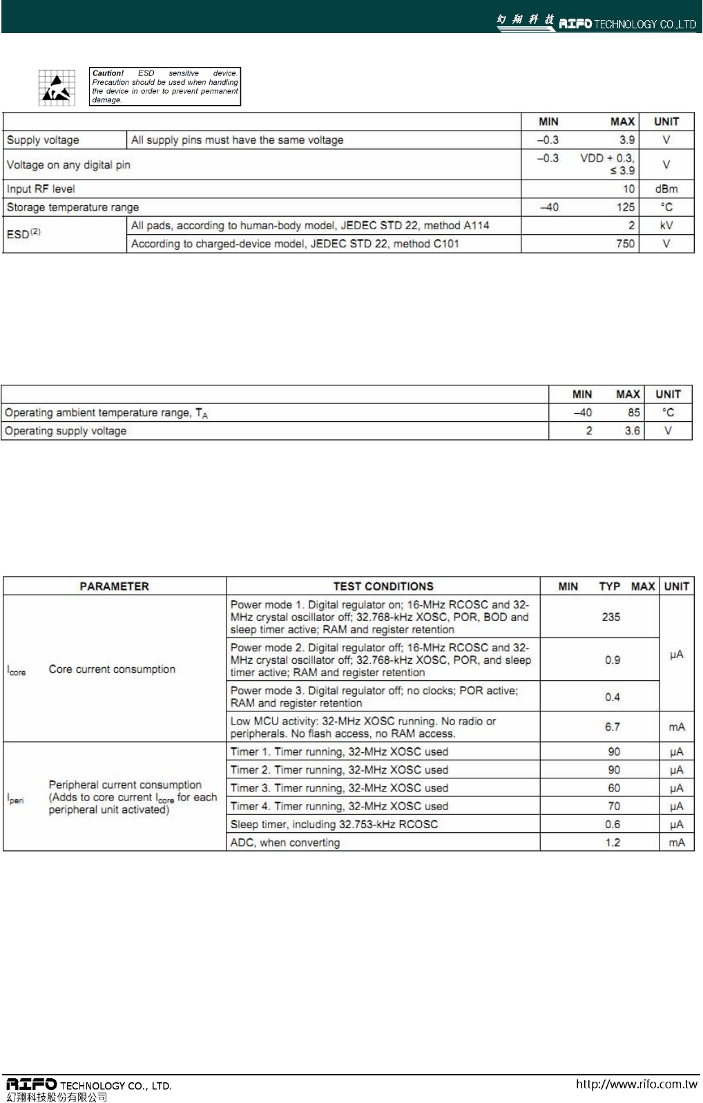
■ Absolute Maximum Ratings
Stresses beyond those listed under Absolute Maximum Ratings may cause permanent damage to the device. These are stress ratings only, and
functional operation of the device at these or any other conditions beyond those indicated under Recommended Operating Conditions is not implied.
Exposure to absolute-maximum-rated conditions for extended periods may affect device reliability.
CAUTION: ESD sensitive device. Precaution should be used when handling the device in order to prevent permanent damage.
■ Recommended Operation Condition
■ Electrical Specifications
● Current Consumption
TA = 25°C and VDD = 3 V
TM41B1412-Fxxx
4
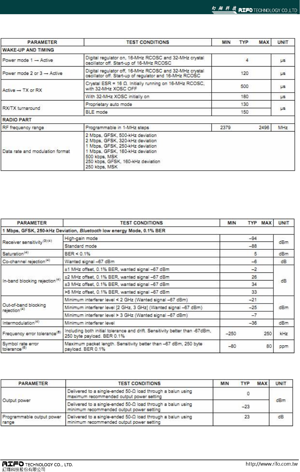
■ General Characteristics
TA = 25°C and VDD = 3 V, unless otherwise noted.
■ RF Characteristics
1Mbps, GFSK, 250-KHz deviation, Bluetooth low energy mode and 1%BER
TM41B1412-Fxxx
5
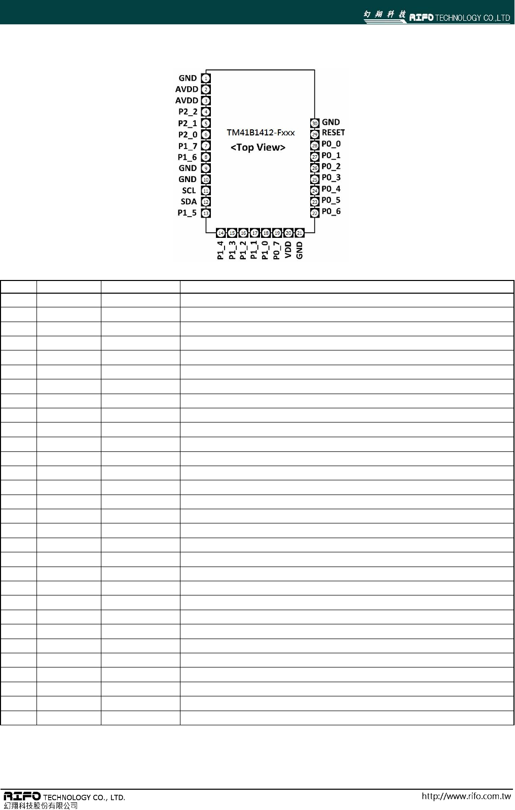
■ TM41B1412-Fxxx RF Module Pin Configuration
Pin #. Pin Name Pin Type Description
1 GND GND Ground
2 AVDD ANALOG POWER 2~3.6V power supply
3 AVDD ANALOG POWER 2~3.6V power supply
4 P2.2 Digital I/O
5 P2.1 Digital I/O
6 P2.0 Digital I/O
7 P1.7 Digital I/O
8 P1.6 Digital I/O
9 GND GND Ground
10 GND GND Ground
11 SCL Digital I/O I2C signal
12 SDA Digital I/O I2C signal
13 P1.5 Digital I/O
14 P1.4 Digital I/O
15 P1.3 Digital I/O
16 P1.2 Digital I/O
17 P1.1 Digital I/O
18 P1.0 Digital I/O
19 P0.7 Digital I/O
20 VDD Digital POWER 2~3.6V power supply
21 GND GND Ground
22 P0.6 Digital I/O
23 P0.5 Digital I/O
24 P0.4 Digital I/O
25 P0.3 Digital I/O
26 P0.2 Digital I/O
27 P0.1 Digital I/O
28 P0.0 Digital I/O
29 RESET RESET Low active
30 GND GND Ground
TM41B1412-Fxxx
6
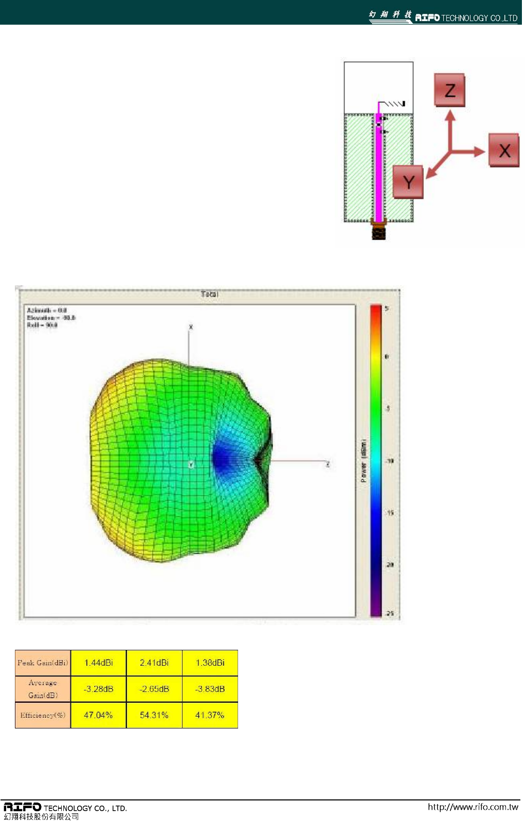
■ Antenna Radiation Pattern
TM41B1412-Fxxx
7
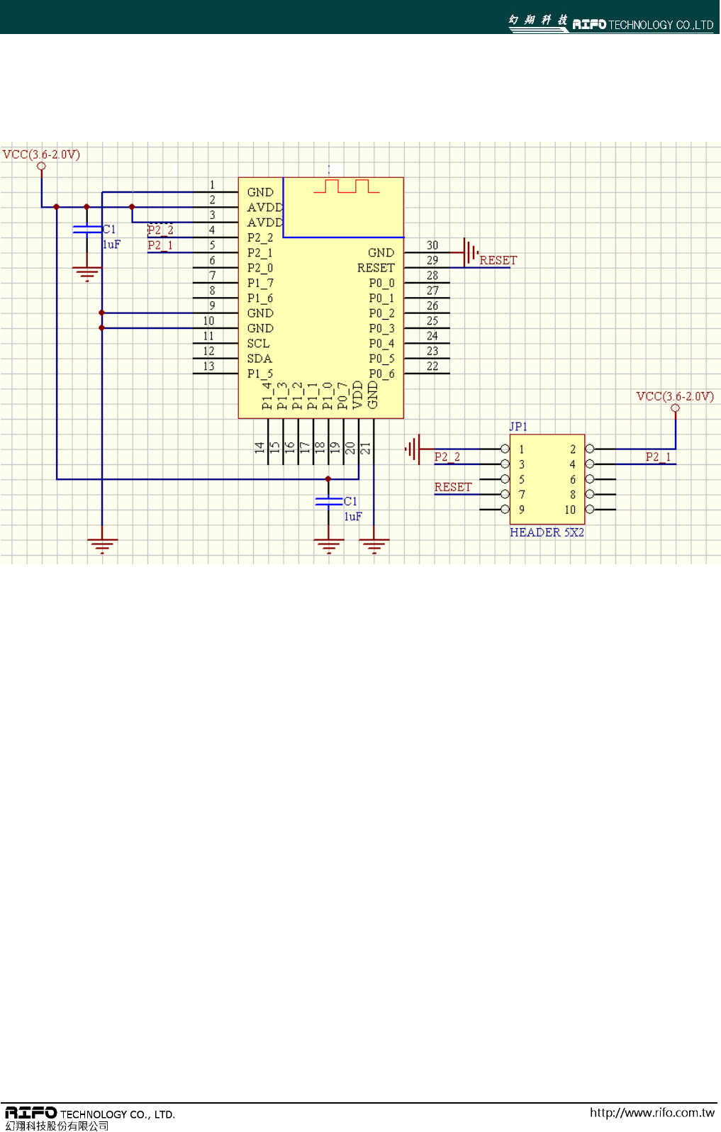
■ TM41B1412-Fxxx RF Module Example Design schematic
Example schematic:
TM41B1412-Fxxx
8
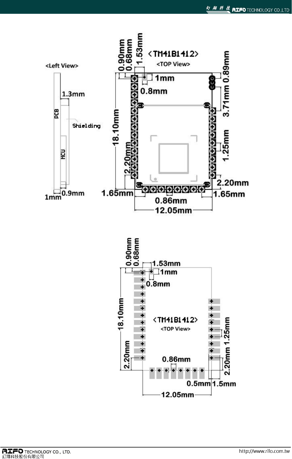
■ TM41B1412-Fxxx RF Module Dimension
■ Recommended PCB layout for Module
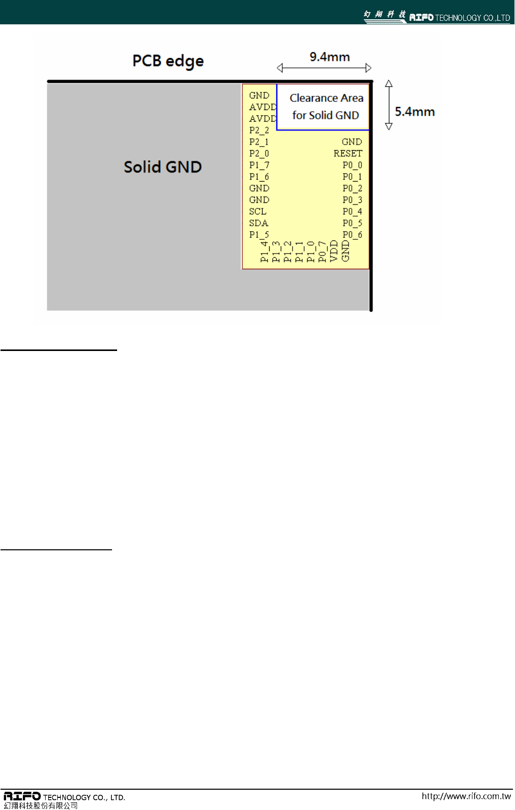
TM41B1412-Fxxx
9
Important FCC notice:
In accordance with FCC Part 15C , this module is listed as a Modular Transmitter device.
Changes or modifications not expressly approved by the manufacturer could void the user’s authority to operate the
equipment.
The antenna of this transmitter must not be co-located or operating in conjunction with any other antenna or
transmitters within a host device, except in accordance with FCC multitransmitter product approval procedures.
FCC Certification only covers the shielded version of the module.
FCC Label Instructions
The outside of final products that contains this module device must display a label
referring to the enclosed module. This exterior label can use wording such as the
following: “Contains Transmitter Module FCC ID: 2AEQ4RIFO
” or “Contains FCC ID: 2AEQ4RIFO
.” Any similar wording that expresses the same meaning may be used.
Additionally, there must be the following sentence on the device, unless it is too small to carry it:
“This device complies with part 15 of the FCC Rules. Operation is subject to the following two conditions:
(1) This device may not cause harmful interference, and (2) this device must accept any interference received,
including interference that may cause undesired operation.”
TM41B1412-Fxxx
1
■ Document History
Revision Date Description/Changes
1.0 2014.04.08 First release
2.0 2014.12.08 update
3.0 2015.05.05 Update dimension & layout guide for pad of external antenna
3.1 2015.05.19
1. Add module name of external antenna
2.Add Important FCC notice & FCC Label Instructions
3.2 2015.06.18 Because Extend Antenna PAD affect External Antenna PAD Performance, so layout guide delete Extend
Antenna PAD
3.3 2015.07.23 Page 9: Add FCC Notify.
■ Address Information