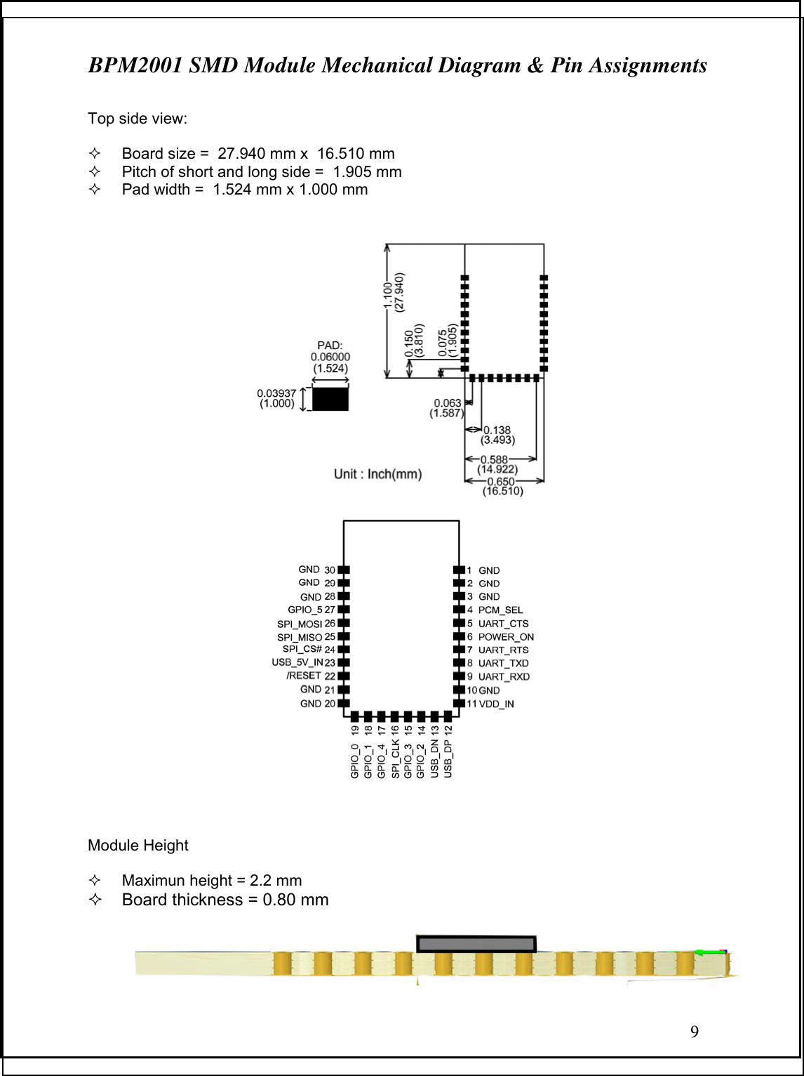
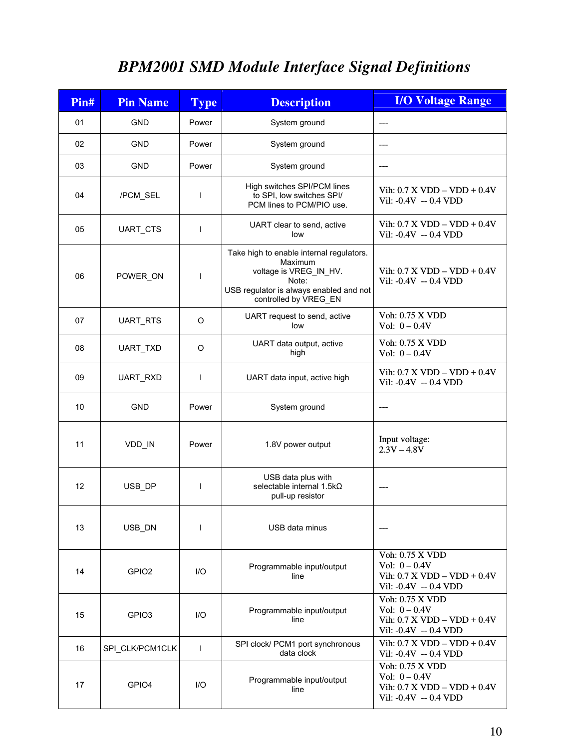
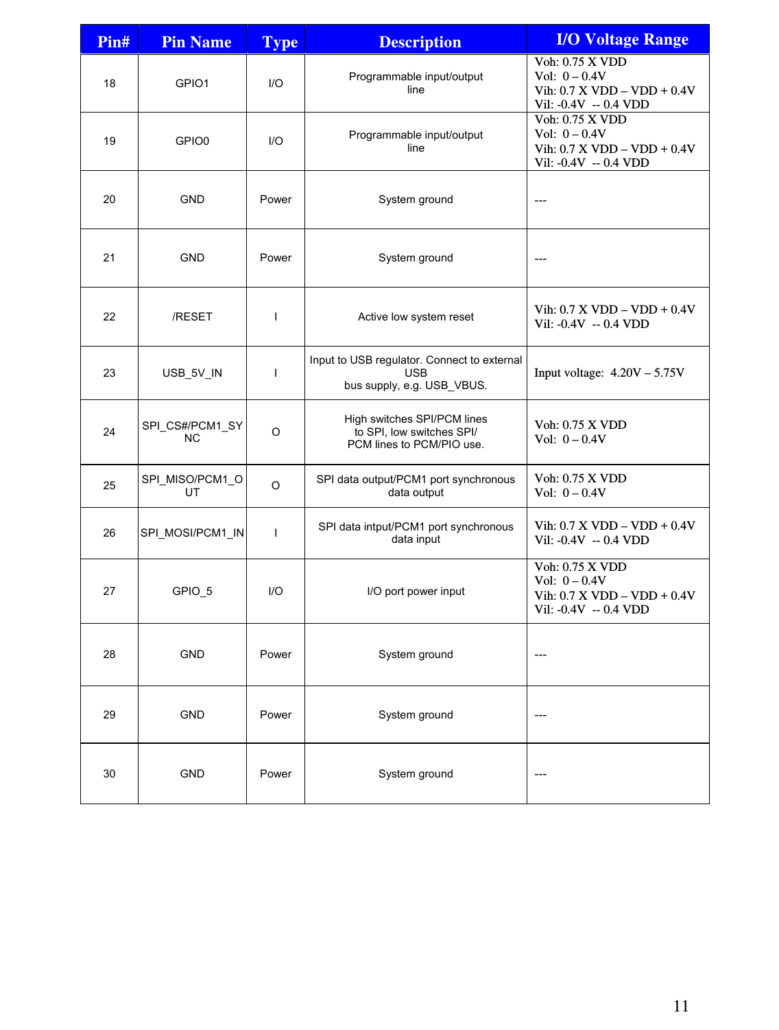
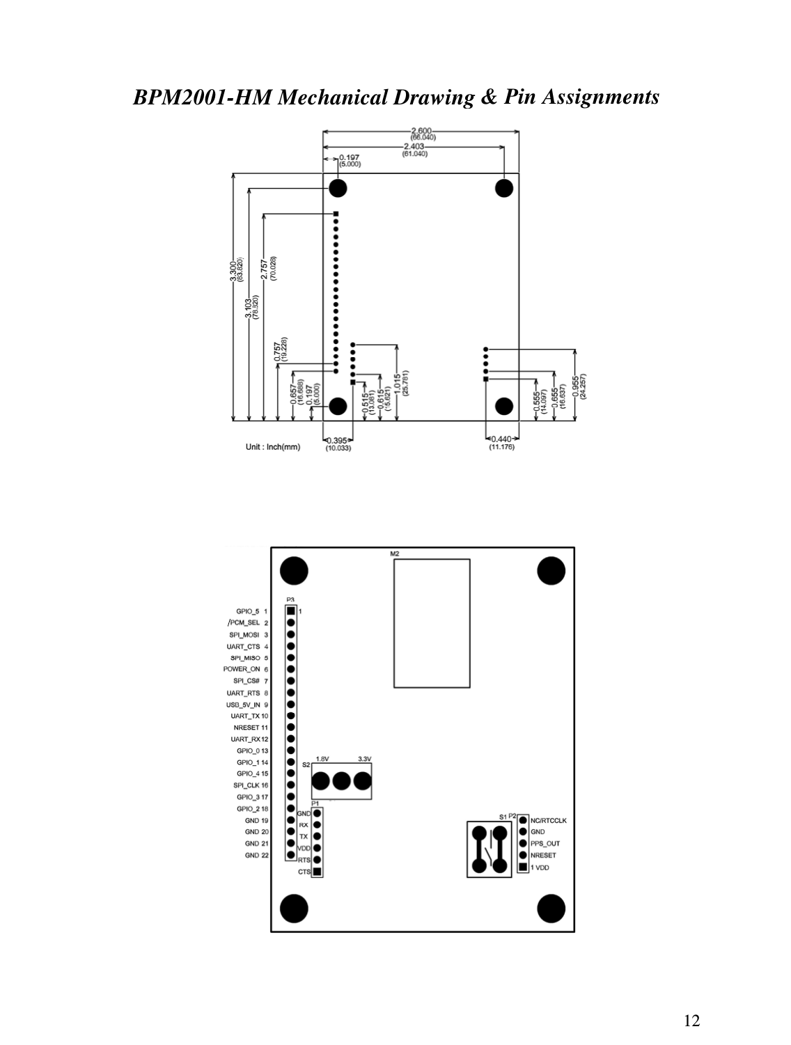
Radicom Research BPM2001 CSR8311 BlueTooth Module User Manual UserMan
Radicom Research Inc CSR8311 BlueTooth Module UserMan
UserManual.wiki
>
Radicom Research
>
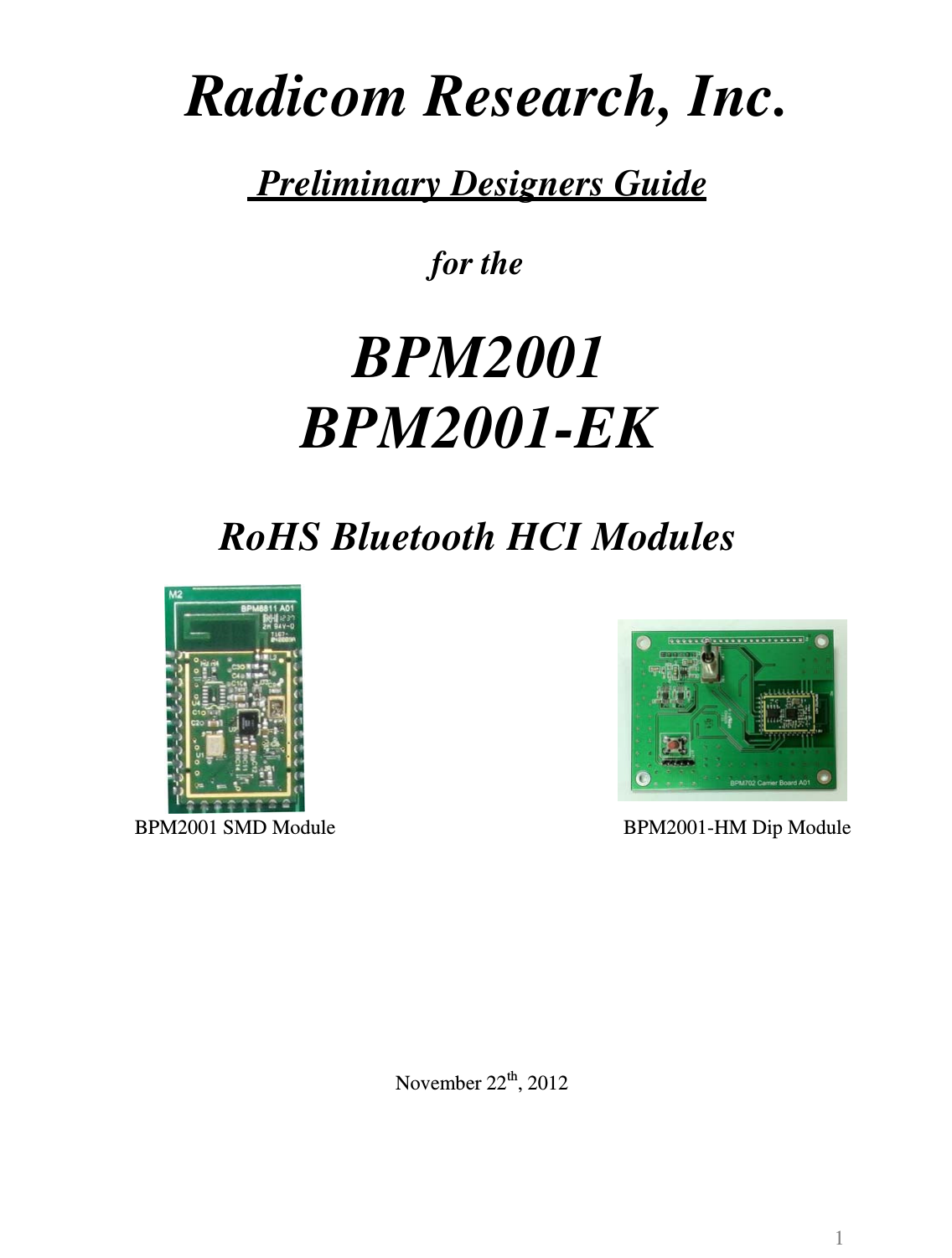
BPM2001 User Manual
UserMan
Navigation menu
Upload a User Manual
Namespaces
Wiki Guide
HTML
PDF
Info
Views
User Manual
Discussion / Help
Navigation