Radicom Research BPM2001 CSR8311 BlueTooth Module User Manual UserMan
Radicom Research Inc CSR8311 BlueTooth Module UserMan
UserMan
Radicom Research, Inc.
Preliminary Designers Guide
for
the
BPM2001
BPM2001-EK
RoHS Bluetooth HCI Modules
BPM2001 SMD Module BPM2001-HM Dip Module
November 22th, 2012
1

Table of Contents
Introduction 3
Features 4
Applications 5
Specifications 6
Electronic Character 7
Model and Ordering Information 7
Layout Design Considerations 8
BPM2001 SMD Module Mechanical Diagram & Pin Assignments 9
BPM2001 SMD Module Interface Signal Definitions 10
BPM2001-HM Mechanical Diagram & Pin Assignments 12
BPM2001-EK Switches & Connector Functional Descriptions 16
Operating the BPM2001-EK Evaluation Kit 17
BPM2001-MB Carrier Board RS232 DE-9 Pin Definitions 17
FCC & IC Label and Model Identification 18
Important Regulatory Compliance and User Information 19
Industry Canada statement: 21
CE Declaration of Conformity 24
Limited Warranty 25
Contacting Radicom 27
Information furnished by Radicom is believed to be accurate and reliable. However Radicom assumes
no responsibility for its use, or any infringement of patents or other rights of third parties that may
result from its use. Radicom reserves the right to change circuitry at any time without notice. This
document is subject to change without notice.
2

3
Introduction
Radicom BPM2001 is a single chip based radio and baseband for Bluetooth v4.0 systems
and Bluetooth low energy. With host software, BPM2001 provides a system fully qualified
to the Bluetooth v4.0 specification for data and voice applications.

4
Features
• Fully qualified Bluetooth Bluetooth® v4.0 system
• Full-speed Bluetooth operation with full piconet and scatternet support
• Class 2 Bluetooth power level supported
• High-sensitivity Bluetooth receiver
• Wideband speech
• SBC encoding
• Low-power selectable 1.2 to 3.6V I/O
• Full-speed USB 2.0 interface
• High-speed UART port (up to 4Mbps)
• 2 x PCM/I2S digital audio interfaces
• Support for IEEE 802®.11 coexistence
• Dual-mode Bluetooth low energy radio
• 3 Bluetooth low energy connections at the same time as basic rate A2DP
• Approx. 27.9mm x 16.5mm FR4 PCB.
• On-board antenna
• -40°C to +85°C temperature operating
• RoHS compliant

5
Applications
• Industrial
• Medical
• For AP Switch, Router, PC, NB, PND, PDA, Mobile devices, USB dongle

6
Specifications
Dimensions 27.94mm x 16.51mm x 2.20mm (BPM2001)
83.73mm x 66.11mm (BPM2001HM)
Device Type Embedded Bluetooth OEM modules
Interface Serial UART / PCM / I2S / USB
Data Link Protocol Bluetooth 4.0
Frequency 2.402 – 2.480 GHz
Transmit Power 6 dBm (typical)
Receiver Sensitivity -92.5dBm (typical)
Bluetooth Class Class 2
Range Up to 10 meters
Security 128-bit encryption (optional)
Power Consumption IDE: 3~6mA / Play: 22~38mA
Power Supply Voltage 1.8V~ 3.6V
Normal Voltage 3.3V
Operating Temperature -40ºC to +85ºC
Environmental RoHS compliant
7
Electronic Character
Minimum Typical Maximum Unit
Operation voltage 1.8 3.3 3.6 V
Output Power 6 dBm
Sensitivity -84
dBm
active mode, VBAT=3.3V 24 mA
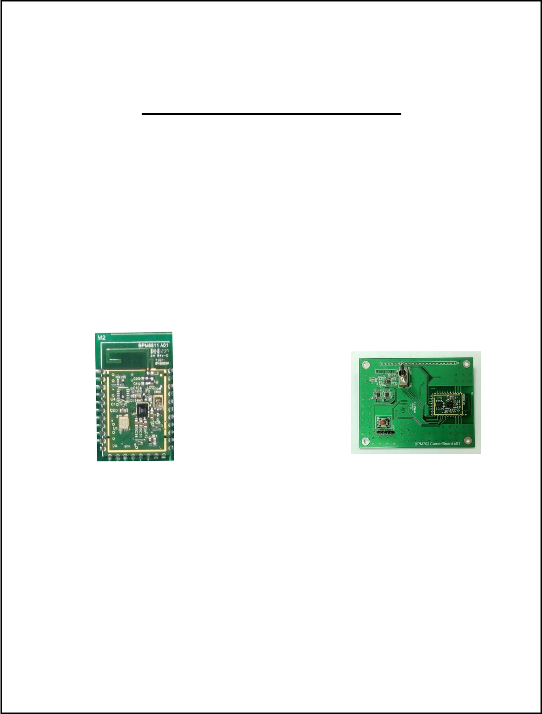
Model and Ordering Information
Model Number Description
BPM2001
Surface mount, class 2, Bluetooth HCI module with on-board
antenna
BPM2001-HM
BPM2001HM-a: DIP, through hole module with on-
b
oard antenna.
BPM2001HM-c: DIP, through hole module with U.FL antenna
connector for external antenna
BPM2001-MB
BPM2001-MB Evaluation PCB
Model: BPM2001-MB
BPM2001-EK
Evaluation Kit. Each kit consists of the following components:
1. BPM2001HM (-a or -c) on a testing board
2. USB cables (A to B)
3. Null modem cables (DB9F to DB9F)
* BPM2001HM-c ships with 1 external antenna and cable.

8
Layout Design Suggestions
•
General Layout Rules- All Printed Circuit Boards must comply with UL94V0
standard for flammability. Always use RoHS compliant Parts and materials.
•
Suggestions for Layout:
1. Do not place Power circuit, X’tal, Inductor, etc near RF area.
2. The bigger Antenna clearance area, the better. The Antenna itself needs to stay away
from any circuit or component at least 2mm. Antenna clearance area means Top and
Bottom both required to be cleared.
3. Do not use metal materials on design where near Antenna area. For example, battery
snaps, USB connector, iron case, etc.
4. Except ground, do not place any circuit below Bluetooth IC. The area below Bluetooth
IC is required to be ground and be connected by through hole.
5. When meeting a turning point, try to make the circuit as smooth as you can.
6. Put all TP (Test-Point) in one area, in order to make easier for a fixture design.
7. Within the acceptance, please make circuit diameter as big as you can.
8. If a position hole is needed, please make them in diagonal location. This design could
make easier for fixture allocation and save cost in fixture designing.
These guidelines are for design reference; real performance still depends on actual
design.
9
BPM2001 SMD Module Mechanical Diagram & Pin Assignments
Top side view:
Board size = 27.940 mm x 16.510 mm
Pitch of short and long side = 1.905 mm
Pad width = 1.524 mm x 1.000 mm
Module Height
Maximun height = 2.2 mm
Board thickness = 0.80 mm

10
BPM2001 SMD Module Interface Signal Definitions
Pin# Pin Name Type Description I/O Voltage Range
01 GND Power System ground ---
02 GND Power System ground ---
03 GND Power System ground ---
04 /PCM_SEL I
High switches SPI/PCM lines
to SPI, low switches SPI/
PCM lines to PCM/PIO use.
Vih: 0.7 X VDD – VDD + 0.4V
Vil: -0.4V -- 0.4 VDD
05 UART_CTS I UART clear to send, active
low
Vih: 0.7 X VDD – VDD + 0.4V
Vil: -0.4V -- 0.4 VDD
06 POWER_ON I
Take high to enable internal regulators.
Maximum
voltage is VREG_IN_HV.
Note:
USB regulator is always enabled and not
controlled by VREG_EN
Vih: 0.7 X VDD – VDD + 0.4V
Vil: -0.4V -- 0.4 VDD
07 UART_RTS O UART request to send, active
low
Voh: 0.75 X VDD
Vol: 0 – 0.4V
08 UART_TXD O UART data output, active
high
Voh: 0.75 X VDD
Vol: 0 – 0.4V
09 UART_RXD I UART data input, active high Vih: 0.7 X VDD – VDD + 0.4V
Vil: -0.4V -- 0.4 VDD
10 GND Power System ground ---
11 VDD_IN Power 1.8V power output Input voltage:
2.3V – 4.8V
12 USB_DP I
USB data plus with
selectable internal 1.5kΩ
pull-up resistor
---
13 USB_DN I USB data minus ---
14 GPIO2 I/O Programmable input/output
line
Voh: 0.75 X VDD
Vol: 0 – 0.4V
Vih: 0.7 X VDD – VDD + 0.4V
Vil: -0.4V -- 0.4 VDD
15 GPIO3 I/O Programmable input/output
line
Voh: 0.75 X VDD
Vol: 0 – 0.4V
Vih: 0.7 X VDD – VDD + 0.4V
Vil: -0.4V -- 0.4 VDD
16 SPI_CLK/PCM1CLK I SPI clock/ PCM1 port synchronous
data clock
Vih: 0.7 X VDD – VDD + 0.4V
Vil: -0.4V -- 0.4 VDD
17 GPIO4 I/O Programmable input/output
line
Voh: 0.75 X VDD
Vol: 0 – 0.4V
Vih: 0.7 X VDD – VDD + 0.4V
Vil: -0.4V -- 0.4 VDD

11
Pin# Pin Name Type Description I/O Voltage Range
18 GPIO1 I/O Programmable input/output
line
Voh: 0.75 X VDD
Vol: 0 – 0.4V
Vih: 0.7 X VDD – VDD + 0.4V
Vil: -0.4V -- 0.4 VDD
19 GPIO0 I/O Programmable input/output
line
Voh: 0.75 X VDD
Vol: 0 – 0.4V
Vih: 0.7 X VDD – VDD + 0.4V
Vil: -0.4V -- 0.4 VDD
20 GND Power System ground ---
21 GND Power System ground ---
22 /RESET I Active low system reset Vih: 0.7 X VDD – VDD + 0.4V
Vil: -0.4V -- 0.4 VDD
23 USB_5V_IN I
Input to USB regulator. Connect to external
USB
bus supply, e.g. USB_VBUS.
Input voltage: 4.20V – 5.75V
24 SPI_CS#/PCM1_SY
NC O
High switches SPI/PCM lines
to SPI, low switches SPI/
PCM lines to PCM/PIO use.
Voh: 0.75 X VDD
Vol: 0 – 0.4V
25 SPI_MISO/PCM1_O
UT O SPI data output/PCM1 port synchronous
data output
Voh: 0.75 X VDD
Vol: 0 – 0.4V
26 SPI_MOSI/PCM1_IN I SPI data intput/PCM1 port synchronous
data input
Vih: 0.7 X VDD – VDD + 0.4V
Vil: -0.4V -- 0.4 VDD
27 GPIO_5 I/O I/O port power input
Voh: 0.75 X VDD
Vol: 0 – 0.4V
Vih: 0.7 X VDD – VDD + 0.4V
Vil: -0.4V -- 0.4 VDD
28 GND Power System ground ---
29 GND Power System ground ---
30 GND Power System ground ---
12
BPM2001-HM Mechanical Drawing & Pin Assignments

13
BPM2001-HM Interface Signal Definitions
P3 Port Pin Assignments
Pin# Pin Name Type Description Voltage Range
1 GPIO_5 I/O I/O port power input
Voh: 0.75 X VDD
Vol: 0 – 0.4V
Vih: 0.7 X VDD – VDD + 0.4V
Vil: -0.4V -- 0.4 VDD
2 /PCM_SEL I
High switches SPI/PCM lines
to SPI, low switches SPI/
PCM lines to PCM/PIO use.
Vih: 0.7 X VDD – VDD + 0.4V
Vil: -0.4V -- 0.4 VDD
3 SPI_MOSI I
SPI data intput/PCM1 port
synchronous
data input
Vih: 0.7 X VDD – VDD + 0.4V
Vil: -0.4V -- 0.4 VDD
4 UART_CTS I UART clear to send, active
low
Vih: 0.7 X VDD – VDD + 0.4V
Vil: -0.4V -- 0.4 VDD
5 SPI_MISO/PCM1_OU
T O
SPI data output/PCM1 port
synchronous
data output
Voh: 0.75 X VDD
Vol: 0 – 0.4V
6 POWER_ON I
Take high to enable internal
regulators. Maximum
voltage is VREG_IN_HV.
Note:
USB l i l bl d d
Vih: 0.7 X VDD – VDD + 0.4V
Vil: -0.4V -- 0.4 VDD
7 SPI_CS# O
High switches SPI/PCM lines
to SPI, low switches SPI/
PCM lines to PCM/PIO use.
Voh: 0.75 X VDD
Vol: 0 – 0.4V
8 UART_RTS O
UART request to send, active
low
Voh: 0.75 X VDD
Vol: 0 – 0.4V
9 USB_5V_IN I
Input to USB regulator. Connect to
external USB
blUSBVBUS
Input voltage: 4.20V – 5.75V
10 UART_TXD O UART data output, active
high
Voh: 0.75 X VDD
Vol: 0 – 0.4V
11 /RESET I Active low system reset Vih: 0.7 X VDD – VDD + 0.4V
Vil: -0.4V -- 0.4 VDD
12 UART_RXD I UART data input, active high Vih: 0.7 X VDD – VDD + 0.4V
Vil: -0.4V -- 0.4 VDD
13 GPIO0 I/O
Programmable input/output
line
Voh: 0.75 X VDD
Vol: 0 – 0.4V
Vih: 0.7 X VDD – VDD + 0.4V
Vil: -0.4V -- 0.4 VDD
14 GPIO1 I/O
Programmable input/output
line
Voh: 0.75 X VDD
Vol: 0 – 0.4V
Vih: 0.7 X VDD – VDD + 0.4V
Vil: -0.4V -- 0.4 VDD
15 GPIO4 I/O
Programmable input/output
line
Voh: 0.75 X VDD
Vol: 0 – 0.4V
Vih: 0.7 X VDD – VDD + 0.4V
Vil: -0.4V -- 0.4 VDD
16 SPI_CLK/PCM1CLK I SPI clock/ PCM1 port synchronous
data clock
Vih: 0.7 X VDD – VDD + 0.4V
Vil: -0.4V -- 0.4 VDD
17 GPIO2 I/O
Programmable input/output
line
Voh: 0.75 X VDD
Vol: 0 – 0.4V
Vih: 0.7 X VDD – VDD + 0.4V
Vil: -0.4V -- 0.4 VDD
18 GPIO3 I/O
Programmable input/output
line
Voh: 0.75 X VDD
Vol: 0 – 0.4V
Vih: 0.7 X VDD – VDD + 0.4V
Vil: -0.4V -- 0.4 VDD

14
Pin# Pin Name Type Description Voltage Range
19 GND Power System ground ---
20 GND Power System ground ---
21 GND Power System ground ---
22 GND Power System ground ---

15
P1 Port Pin Assignments
Pin# Pin Name Type Description Voltage Range
1 UART_CTS I UART clear to send, active
low
Vih: 0.7 X VDD – VDD + 0.4V
Vil: -0.4V -- 0.4 VDD
2 UART_RTS O
UART request to send, active
low
Voh: 0.75 X VDD
Vol: 0 – 0.4V
3 VDD I HM Power In Input voltage: 4.30V – 5.75V
4 UART_TXD O UART data output, active
high
Voh: 0.75 X VDD
Vol: 0 – 0.4V
4 UART_RXD I UART data input, active high Vih: 0.7 X VDD – VDD + 0.4V
Vil: -0.4V -- 0.4 VDD
6 GND Power System ground ---
16
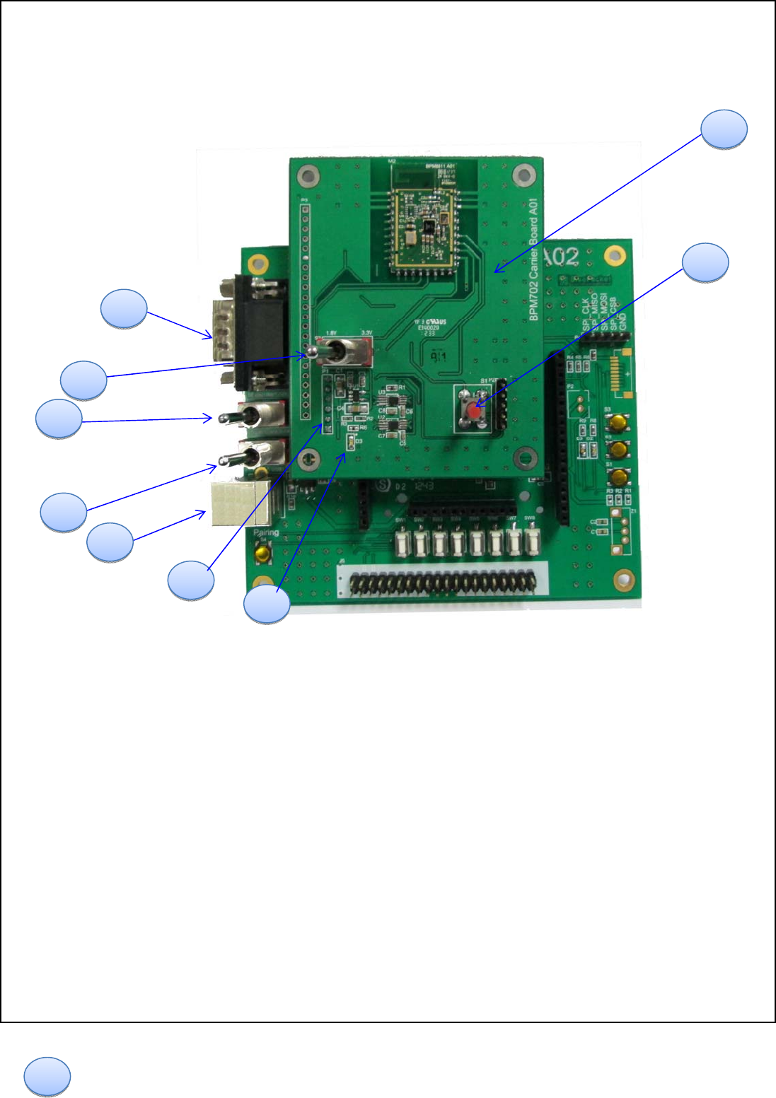
Operating the BPM2001-EK Evaluation Kit
The BPM2001-MB Evaluation PCB has white silkscreen legend located by the switches and connectors
described below.
1. USB 5V slot (USB1)
2. Main board power switch (S5)
3. UART enable/disable switch (S6)
4. RS232 male DE-9 connector (J7)
5. BPM2001-HM carrier board with module
6. UART and power interface header (P1)
7. HM board power switch only for 1.8V (S2)
8. Reset push button (S1)
9. HM Power indicator (D3)
4
3
2
5
1
6
7
8
9

17
Operating the BPM2001-EK Evaluation Kit
-On PC (Master):
1. Connect UART cable to PC com port and supply power
2. Execute "cmd" under Windows
3. cd "c:\Program Files\CSR\BlueSuite 2.4.8"
4. btcli com1 bcsp 115200
5. Verify "command_status pending nhcp:0x01 nop"
6. Type "rbn" and verify displayed strings (8 lines)
7. Type exec "d:\d-drive\gps\csr8311\8311.btcli"
8. Wait for "*** HCI TRANSPORT FAILED ***"
9. Type "restart"
10.Verify "command_status pending nhcp:0x01 nop"
11.Type "i" to start inquiry
12.Type "cc 0X000000001"(BD Address)
13.Type"acl acl0 “ABCD” "
-On PC (Slave):
1. Connect UART cable to PC com port and supply power
2. Execute "cmd" under Windows
3. cd "c:\Program Files\CSR\BlueSuite 2.4.8"
4. btcli com1 bcsp 115200
5. Verify "command_status pending nhcp:0x01 nop"
6. Type "rbn" and verify displayed strings (8 lines)
7. Type exec "d:\d-drive\gps\csr8311\8311.btcli"
8. Wait for "*** HCI TRANSPORT FAILED ***"
9. Type "restart"
10.Verify "command_status pending nhcp:0x01 nop"
11.Type " slave " to slave mode
BPM2001-MB Carrier Board RS232 DE-9 Pin Definitions
UART interface is used for firmware download and debug purpose. The DE-9 pin definitions of the
BPM2001-MB RS232 Serial Connector are as follows:
1. DCD: Input, Carrier Detect
2. RXD: Input, Received Data
3. TXD: Output, Transmit data
4. DTR: Output, Data Terminal ready
5. GND: Ground
6 DSR: Input, Data Set Ready
7. RTS: Output, Request to Send
8. CTS: Input, Clear to Send
9. RI: Input, Ring Indicator
18
FCC & IC Label and Model Identification
The BPM2001 module family is FCC Part 15 and IC (Industry Canada) certified. The BPM2001 is
also CE marked. The modules are labeled with the BPM2001 module model number and FCC Part
15 ID, IC registration number and CE mark. The label can be found on top of the metal shielding on
the BPM2001 Module.
Location:
Radicom Research Inc.
Model: BPM2001
FCC ID: K7T-BPM2001
IC: 2377A-BPM2001
Label
Module board

19
Federal Communication Commission Interference Statement
This equipment has been tested and found to comply with the limits for a Class B digital device,
pursuant to Part 15 of the FCC Rules. These limits are designed to provide reasonable protection
against harmful interference in a residential installation. This equipment generates, uses and can
radiate radio frequency energy and, if not installed and used in accordance with the instructions, may
cause harmful interference to radio communications. However, there is no guarantee that interference
will not occur in a particular installation. If this equipment does cause harmful interference to radio or
television reception, which can be determined by turning the equipment off and on, the user is
encouraged to try to correct the interference by one of the following measures:
- Reorient or relocate the receiving antenna.
- Increase the separation between the equipment and receiver.
- Connect the equipment into an outlet on a circuit different from that
to which the receiver is connected.
- Consult the dealer or an experienced radio/TV technician for help.
FCC Caution: Any changes or modifications not expressly approved by the party responsible for
compliance could void the user's authority to operate this equipment.
This device complies with Part 15 of the FCC Rules. Operation is subject to the
following two conditions: (1) This device may not cause harmful interference, and (2)
this device must accept any interference received, including interference that may
cause undesired operation.
IMPORTANT NOTE:
FCC Radiation Exposure Statement:
The product comply with the US portable RF exposure limit set forth for an uncontrolled environment
and are safe for intended operation as described in this manual. The further RF exposure reduction
can be achieved if the product can be kept as far as possible from the user body or set the device to
lower output power if such function is available.
This transmitter must not be co-located or operating in conjunction with any other antenna or
transmitter.

20
This device is intended only for OEM integrators under the following conditions:
1) The transmitter module may not be co-located with any other transmitter or antenna,
As long as 1 condition above is met, further transmitter test will not be required. However, the OEM
integrator is still responsible for testing their end-product for any additional compliance
requirements required with this module installed
IMPORTANT NOTE
In the event that these conditions can not be met (for example certain laptop configurations or co-
location with another transmitter), then the FCC authorization is no longer considered valid and the
FCC ID can not be used on the final product. In these circumstances, the OEM integrator will be
responsible for re-evaluating the end product (including the transmitter) and obtaining a separate
FCC authorization.
End Product Labeling
The final end product must be labeled in a visible area with the following: “Contains FCC ID: K7T-
BPM2001”.
Manual Information to the End User
The OEM integrator has to be aware not to provide information to the end user regarding how to
install or remove this RF module in the user’s manual of the end product which integrates this
module.
The end user manual shall include all required regulatory information/warning as show in this
manual.
21
Industry Canada statement:
This device complies with Industry Canada licence-exempt RSS standard(s). Operation is subject to
the following two conditions:
(1) this device may not cause interference, and
(2) this device must accept any interference, including interference that may cause undesired
operation of the device.
Le présent appareil est conforme aux CNR d'Industrie Canada applicables aux appareils radio
exempts de licence. L'exploitation est autorisée aux deux conditions suivantes :
(1) l'appareil ne doit pas produire de brouillage, et
(2) l'utilisateur de l'appareil doit accepter tout brouillage radioélectrique subi, même si le brouillage est
susceptible d'en compromettre le fonctionnement.
Radiation Exposure Statement:
The product comply with the Canada portable RF exposure limit set forth for an uncontrolled
environment and are safe for intended operation as described in this manual. The further RF
exposure reduction can be achieved if the product can be kept as far as possible from the user body
or set the device to lower output power if such function is available.
Déclaration d'exposition aux radiations:
Le produit est conforme aux limites d'exposition pour les appareils portables RF pour les Etats-Unis et
le Canada établies pour un environnement non contrôlé. Le produit est sûr pour un fonctionnement tel
que décrit dans ce manuel. La réduction aux expositions RF peut être augmentée si l'appareil peut
être conservé aussi loin que possible du corps de l'utilisateur ou que le dispositif est réglé sur la
puissance de sortie la plus faible si une telle fonction est disponible.
22
This device is intended only for OEM integrators under the following conditions:
1) The transmitter module may not be co-located with any other transmitter or antenna.
As long as 1 condition above are met, further transmitter test will not be required. However, the OEM
integrator is still responsible for testing their end-product for any additional compliance requirements
required with this module installed.
Cet appareil est conçu uniquement pour les intégrateurs OEM dans les conditions suivantes:
1) Le module émetteur peut ne pas être coïmplanté avec un autre émetteur ou antenne.
Tant que les 1 condition ci-dessus sont remplies, des essais supplémentaires sur l'émetteur ne seront
pas nécessaires. Toutefois, l'intégrateur OEM est toujours responsable des essais sur son produit
final pour toutes exigences de conformité supplémentaires requis pour ce module installé.
IMPORTANT NOTE:
In the event that these conditions can not be met (for example certain laptop configurations or co-
location with another transmitter), then the Canada authorization is no longer considered valid and the
IC ID can not be used on the final product. In these circumstances, the OEM integrator will be
responsible for re-evaluating the end product (including the transmitter) and obtaining a separate
Canada authorization.
NOTE IMPORTANTE:
Dans le cas où ces conditions ne peuvent être satisfaites (par exemple pour certaines configurations
d'ordinateur portable ou de certaines co-localisation avec un autre émetteur), l'autorisation du Canada
n'est plus considéré comme valide et l'ID IC ne peut pas être utilisé sur le produit final. Dans ces
circonstances, l'intégrateur OEM sera chargé de réévaluer le produit final (y compris l'émetteur) et
l'obtention d'une autorisation distincte au Canada.
23
End Product Labeling
The final end product must be labeled in a visible area with the following: “Contains IC:2377A-
BPM2001”.
Plaque signalétique du produit final
Le produit final doit être étiqueté dans un endroit visible avec l'inscription suivante: "Contient des IC:
2377A-BPM2001".
Manual Information to the End User
The OEM integrator has to be aware not to provide information to the end user regarding how to
install or remove this RF module in the user’s manual of the end product which integrates this module.
The end user manual shall include all required regulatory information/warning as show in this manual.
Manuel d'information à l'utilisateur final
L'intégrateur OEM doit être conscient de ne pas fournir des informations à l'utilisateur final quant à la
façon d'installer ou de supprimer ce module RF dans le manuel de l'utilisateur du produit final qui
intègre ce module.
Le manuel de l'utilisateur final doit inclure toutes les informations réglementaires requises et
avertissements comme indiqué dans ce manuel.

24
CE Declaration of Conformity
For the following equipment:
Radicom Research Inc. Bluetooth Module
Model(s): BPM2001
are herewith confirmed to comply with the requirements set out in the Council (European
parliament) Directive on theApproximation of the Laws of the
Member States relating to Electromagnetic Compatibility of Radio and Telecom device
(1999/5/CE).
For the evaluation regarding this Directive, the following standards were applied:
EN 300 328 V1.8.1
EN 301 489-1 V1.9.2
EN 301 489-17 V2.2.1
EN 60950-1 2006+A11:2009+A1:2010+A12:2011
EN 62311: 2008
EN 61000-3-2 : 2006/A2:2009
EN 61000-3-3 : 2008
This equipment is marked with and can be used throughout the European community.
Europe – R&TTE Compliance Statement:
Hereby, Radicom Research Inc. declares that this equipment complies with the essential
requirements
and other relevant provisions of DIRECTIVE 1999/5/CE OF THE EUROPEAN PARLIAMENT
AND THE COUNCIL of March 9, 1999 on radio equipment and telecommunication
terminal Equipment and the mutual recognition of their conformity (R&TTE).

Limited Warranty
Warranty Coverage and Duration
Radicom Research, Inc. (“RRI”) warrants to the original purchaser its RRI-manufactured
products (“Product”) against defects in material and workmanship under normal use and
service for a period of one year from the date of delivery.
During the applicable warranty period, at no charge, RRI will, at its option, either repair,
replace or refund the purchase price of this Product, provided it is returned in accordance
with the terms of this warranty to RRI. Repair, at the option of RRI, may include the
replacement of parts, boards or other components with functionally equivalent
reconditioned or new parts, boards or other components. Replaced parts, boards or other
components are warranted for the balance of the original applicable warranty period. All
replaced items shall become the property of RRI.
RRI MAKES NO GUARANTEE OR WARRANTY THAT THE PRODUCT WILL
PREVENT OCCURRENCES, OR THE CONSEQUENCES THEREOF, WHICH THE
PRODUCT IS DESIGNED TO DETECT.
This expressed limited warranty is extended by RRI to the original end-user purchaser
only, and is not assignable or transferable to any other party. This is the complete
warranty for the Product manufactured by RRI, and RRI assumes no obligation or
liability for additions or modifications to this warranty. In no case does RRI warrant the
installation, maintenance or service of the Product.
RRI is not responsible in any way for any ancillary equipment not furnished by RRI that
is attached to or used in connection with the Product, or for operation of the Product with
any ancillary equipment, and all such equipment is expressly excluded from this warranty.
Because of wide variations in topographical and atmospheric conditions,
which may require availability of repeater stations or of particular radio frequencies, RRI
assumes no liability for range, coverage or suitability of the Product for any particular
application. Buyer acknowledges that RRI does not know a particular purpose for which
buyer wants the product, and that buyer is not relying on RRI’s skill and judgment to
select or furnish suitable goods.
What this Warranty does NOT Cover:
(a) Defects or damage resulting from use of the Product in other than its normal and
customary manner.
(b) Defects or damage from misuse, accident or neglect.
(c) Defects of damage from improper testing, operation, maintenance, installation,
alteration, modification or adjustment.
(d) Disassembly or repair of the Product in such a manner as to adversely affect
performance or prevent adequate inspection and testing to verify any warranty claim.
(e) Any Product that has had its serial number or date code removed or made illegible.
25

How to Receive Warranty Service:
To obtain warranty service, contact RRI by phone (408)383-9006 for your sales
representative or email to sales@radi.com for an RMA (Return Merchandise
Authorization) number. Deliver or send the Product, transportation and insurance prepaid
to RRI, with the RMA number clearly marked on the outside of the package.
General Provision
This warranty sets forth the full extent of RRI’s responsibilities regarding the Product.
Repair, replacement or refund of the purchase price, at RRI’s option, is the exclusive
remedy.
THIS WARRANTY IS GIVEN IN LIEU OF ALL OTHER EXPRESSED
WARRANTIES. ANY APPLICABLE IMPLIED WARRANTIES, INCLUDING
WITHOUT LIMITATION, THE IMPLIED WARRANTY OF MERCHANTABILITY,
ARE LIMITED TO THE DURATION OF THIS LIMITED WARRANTY. TO THE
FULLEST EXTENT PERMITTED BY LAW, RRI DISCLAIMS ANY LIABILITY
FOR DAMAGES IN EXCESS OF THE PURCHASE PRICE OF THE PRODUCT, FOR
ANY LOSS OF USE, LOSS OF TIME, INCONVENIENCE, COMMERCIAL LOSS,
LOST PROFITS OR SAVING OR OTHER INCIDENTAL, SPECIAL OR
CONSEQUENTIAL DAMAGES ARISING OUT OF THE USE OR INABILITY TO
USE OR FAILURE OF SUCH PRODUCT.
26

Contacting Radicom Research
If more information or technical support is needed, please contact us:
2148 Bering Drive
San Jose, CA. 95131
Telephone: (408) 383 9006
Fax: (408) 383 9007
or
e-mail: sales@radi.com
http://www.radi.com/
27