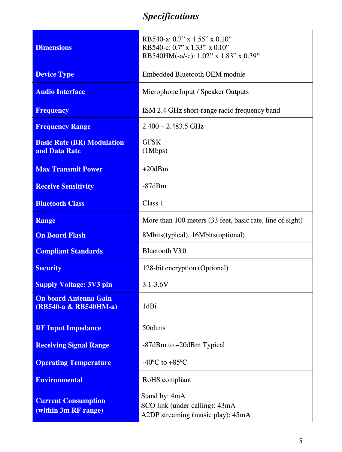
Radicom Research RB540 Class 1 BT audio module User Manual
Radicom Research Inc Class 1 BT audio module Users Manual
UserManual.wiki
>
Radicom Research
>
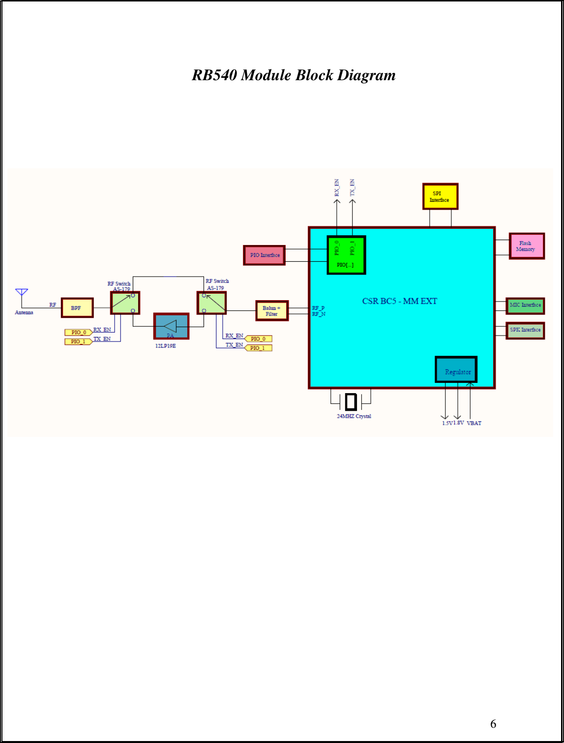
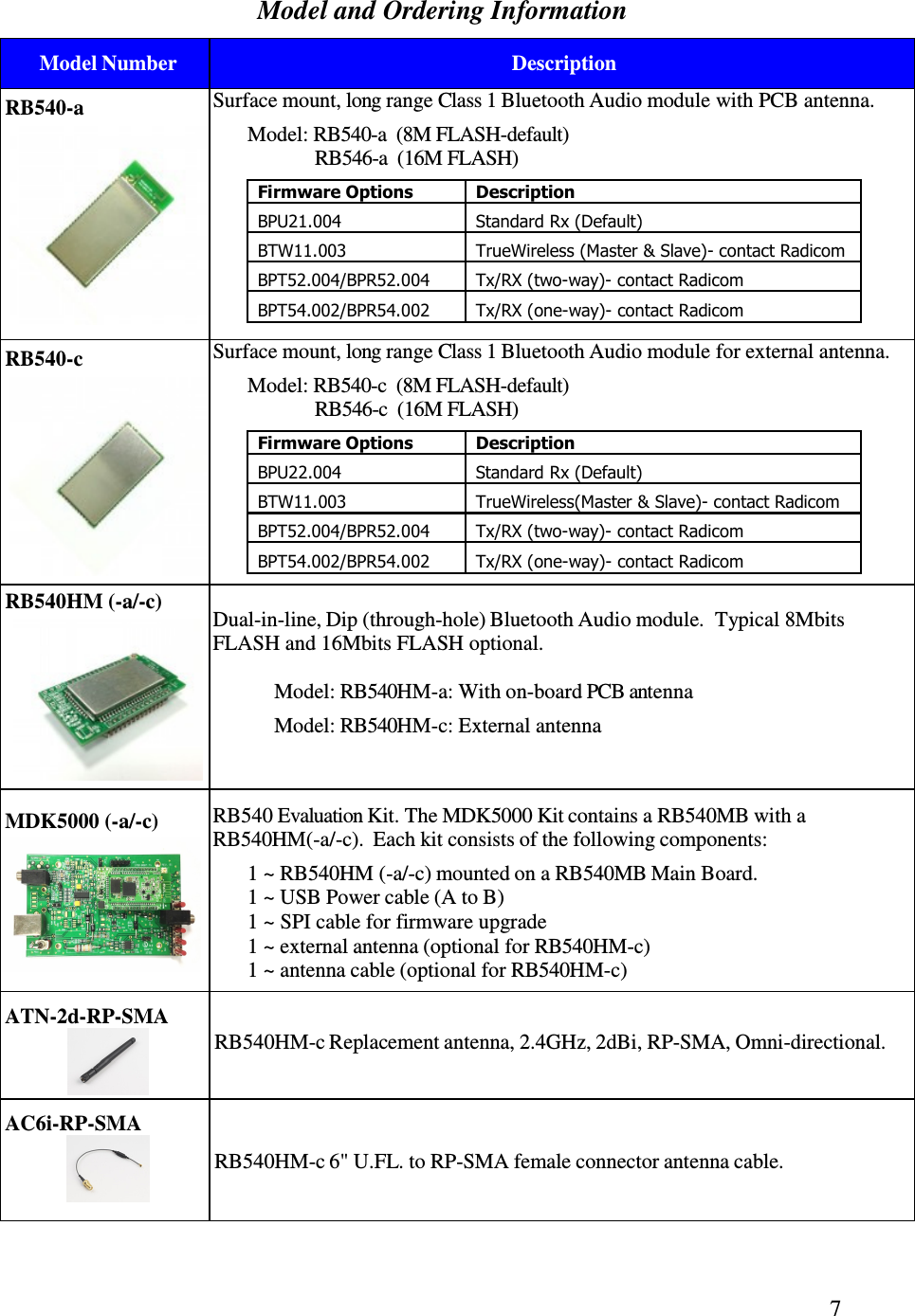
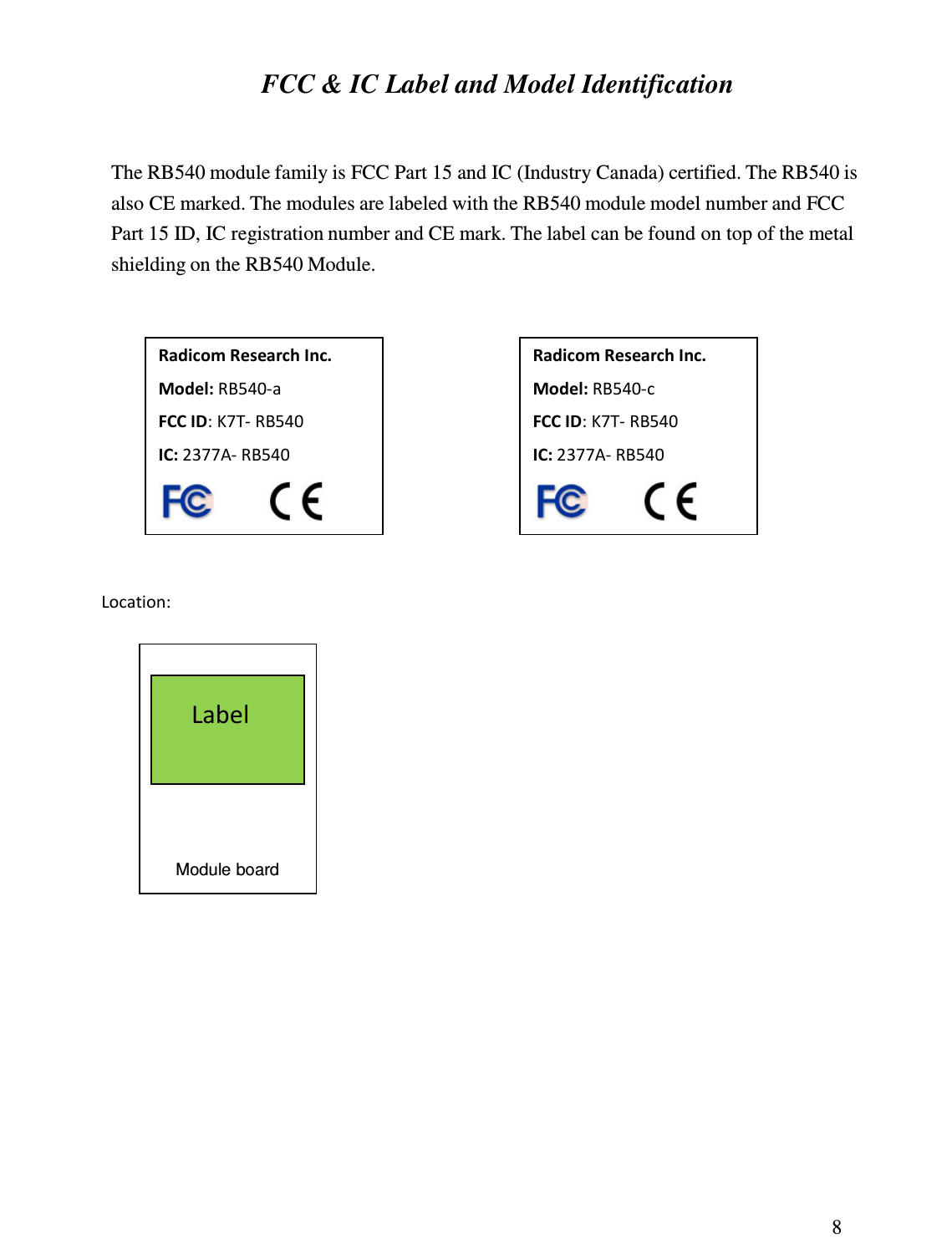
RB540 User Manual
Users Manual
Navigation menu
Upload a User Manual
Namespaces
Wiki Guide
HTML
PDF
Info
Views
User Manual
Discussion / Help
Navigation