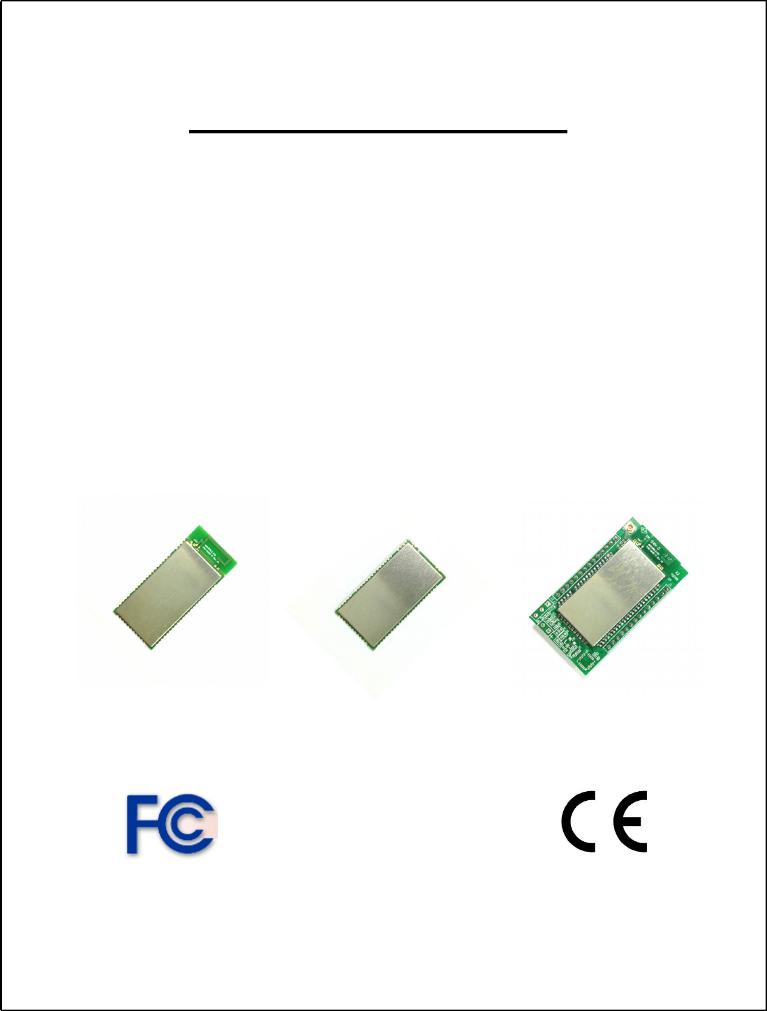
Radicom Research RB540 Class 1 BT audio module User Manual
Radicom Research Inc Class 1 BT audio module Users Manual
Users Manual
Radicom Research, Inc.
Preliminary Designer’s Guide
for the
RB540(-a/-c)
MDK5000 Kit
RoHS Serial TTL Bluetooth Modules
RoHS
Compliant
November 21, 2014
RB540-a RB540-c RB540HM(-a/-c)

Table of Contents
Introduction ...................................................................................................... 3
Features ............................................................................................................ 4
Applications ..................................................................................................... 4
Specifications ................................................................................................... 5
RB540 Module Block Diagram ......................................................................... 6
Model and Ordering Information ....................................................................... 7
FCC & IC Label and Model Identification ........................................................ 8
Federal Communication Commission Interference Statement ............................ 9
Industry Canada Statement ............................................................................... 11
CE Declaration of Conformity .......................................................................... 14
Layout Design Considerations .......................................................................... 15
RB540 Series SMD Module Mechanical Diagram & Pin Assignments .............. 16
Recommended RB540-c SMD Module PCB Layout Dimension ............................. 17
Recommended RB540-a SMD Module PCB Layout Dimension ............................. 18
RB540 Series SMD Module Interface Signal Definitions .................................. 19
RB540HM (-a/-c) Mechanical Drawing .......................................................................... 22
RB540HM (-a/-c) Interface Signal Definitions .................................................. 23
RB540MB Development Board Figure & Functional Descriptions .................... 23
Operating the RB540MB for Standard RX ........................................................... 24
Operating the RB540MB for TrueWireless Stereo Sound .................................. 25
Operating the RB540MB for Tx/Rx (two-way SCO Link) .............................................. 26
Operating the RB540MB for Tx/Rx (one-way A2DP) .................................................... 27
Upgrading the Firmware in the RB540 series ..................................................... 29
SPI Programming Connector (JP1) ................................................................... 29
Suggested Microphone Circuit .......................................................................... 30
Suggested Differential to Single End Circuit ......................................................... 30
Suggested LED Circuit ...................................................................................... 30
Limited Warranty ............................................................................................. 31
Contacting Radicom........................................................................................... 33
Information furnished by Radicom is believed to be accurate and reliable. However Radicom assumes
no responsibility for its use, or any infringement of patents or other rights of third parties that may
result from its use. Radicom reserves the right to change circuitry at any time without notice. This
document is subject to change without notice.

3
Introduction
Thank you for purchasing Radicom’s RB540 series Class 1 Bluetooth multimedia module.
We are committed to providing you quality service and technical support. The RB540
series module is designed to meet requirements for long-range wireless audio
functionality. The RB540 series offers a quick and simple solution for adding wireless
audio Bluetooth communications to OEM’s products.
The RB540 series are embedded Class 1 Bluetooth modules using BlueCore5-External
Chipset from CSR, the leader in Bluetooth chipsets. These Bluetooth radio modules
combine Bluetooth Basic Rate (BR) technology to provide increased throughput, reduced
battery consumption and improved security. They also provide faster pairing and allow
superior performance in the presence of interference from 802.11 WiFi wireless devices
and other 2.4GHz radios.
The RB540 series has on board flash memory available to upgrade the module’s
firmware, modify parameters, or implement custom features. Radicom can modify the
firmware to meet OEM requirements and create custom Bluetooth functionality to meet
your specific needs.
The RB540 series supports AV, handset, hands-free wireless profiles to create a
connection between two devices such as MP3/CD players, mobile phones, tablet,
desktop or notebook computers, PDA…etc.
Containing all of the necessary software stacks and hardware I/O, the RB540 series is
perfect
for designing a custom Bluetooth Audio product by simply adding components
such as a microphone, speaker, LED, buttons, headset housing, etc.

4
Features
• Bluetooth 3.0 support
•
Class 1 radio, transmission power 20dbm Max
•
AV profile, HSP (Head-Set Profile), and HFP (Hands-Free Profile)
•
AVRCP (Audio Video Remote Control Profile)
•
GAP (Generic Access Protocol)
•
SDP (Service Discovery Protocol)
•
A2DP (Advanced Audio Distribution Profile)
•
L2CAP (Logical Link Control and Adaptation Protocol)
•
SPP (Serial Port Profile) & HID (Human Interface Device Profile) Optional support
•
Up to 16Mbits flash memory on board (firmware dependent ~ 8Mbits typical)
•
Secure communications with 128-bit encryption
•
Supports 802.11 wireless co-existence
•
Enhanced Audibility and Noise Cancellation
•
Integrated switching regulator
•
RB540HM-a Onboard antenna or RB540HM-c with an U.FL connector for external antenna
•
64MIPS Kalimba DSP co-processor
•
16-bit internal stereo CODE-95dB SNR for DAC
• True Bluetooth Stereo Sound (Optional firmware required)
Applications
•
High quality stereo wireless headsets
•
High quality mono headsets
•
Hands-free car kits
•
Wireless speakers
•
VOIP headsets
•
Bluetooth-Enable Automotive wireless Gateways
•
Custom application specific Firmware is feasible. Contact Radicom for more information.

5
Specifications
Dimensions
RB540-a: 0.7” x 1.55” x 0.10”
RB540-c: 0.7” x 1.33” x 0.10”
RB540HM(-a/-c): 1.02” x 1.83” x 0.39”
Device Type Embedded Bluetooth OEM module
Audio Interface Microphone Input / Speaker Outputs
Frequency
ISM 2.4 GHz short-range radio frequency band
Frequency Range 2.400 – 2.483.5 GHz
Basic Rate (BR) Modulation
and Data Rate
GFSK
(1Mbps)
Max Transmit Power +20dBm
Receive Sensitivity -87dBm
Bluetooth Class Class 1
Range More than 100 meters (33 feet, basic rate, line of sight)
On Board Flash 8Mbits(typical), 16Mbits(optional)
Compliant Standards Bluetooth V3.0
Security 128-bit encryption (Optional)
Supply Voltage: 3V3 pin 3.1-3.6V
On board Antenna Gain
(RB540-a & RB540HM-a)
1dBi
RF Input Impedance 50ohms
Receiving Signal Range -87dBm to –20dBm Typical
Operating Temperature -40ºC to +85ºC
Environmental RoHS compliant
Current Consumption
(within 3m RF range)
Stand by: 4mA
SCO link (under calling): 43mA
A2DP streaming (music play): 45mA
6
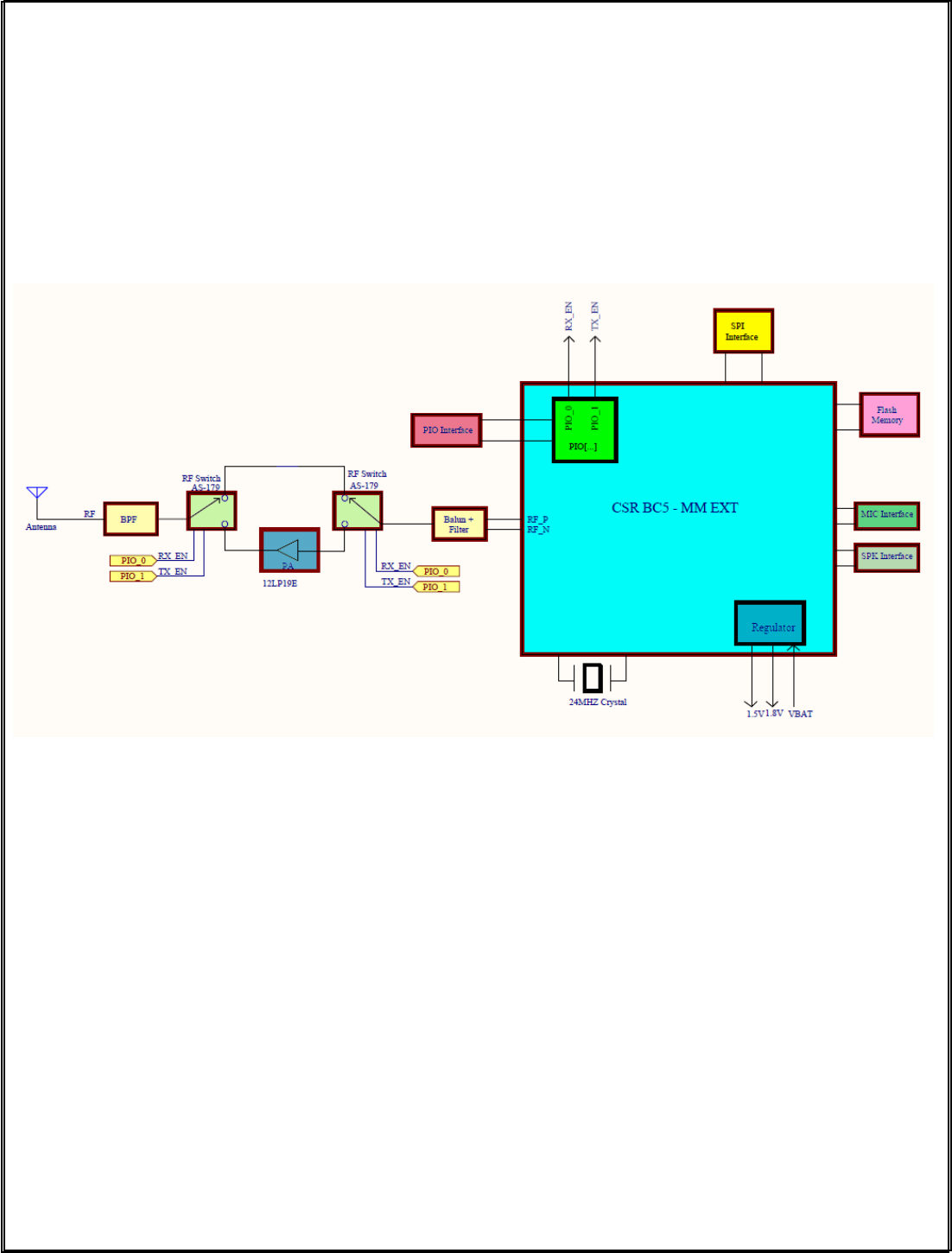
RB540 Module Block Diagram
7
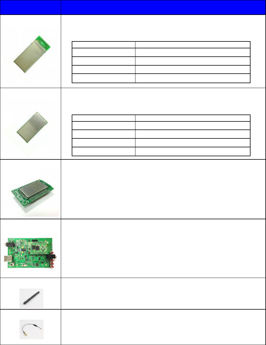
Model and Ordering Information
Model Number
Description
RB540-a
Surface
m
ount,
long
range
Class 1
Bluetooth
Audio
m
odule with PCB antenna.
Model: RB540-a (8M FLASH-default)
RB546-a (16M FLASH)
!"#""#$
%&% &'(#!()!"#""#$
%&% &'#!()!"#""#$
RB540-c
Surface
m
ount,
long
range
Class 1
Bluetooth
Audio
m
odule
for external antenna
.
Model: RB540-c (8M FLASH-default)
RB546-c (16M FLASH)
!"#""#$
%&% &'(#!()!"#""#$
%&% &'#!()!"#""#$
RB540HM (-a/-c)
Dual-in-line, Dip (through-hole) Bluetooth Audio module. Typical 8Mbits
FLASH and 16Mbits FLASH optional.
Model: RB540HM-a: With on-board PCB antenna
Model: RB540HM-c: External antenna
MDK5000 (-a/-c)
RB540 Evaluation Kit. The MDK5000 Kit contains a RB540MB with a
RB540HM(-a/-c). Each kit consists of the following components:
1 ~ RB540HM (-a/-c) mounted on a RB540MB Main Board.
1 ~ USB Power cable (A to B)
1 ~ SPI cable for firmware upgrade
1 ~ external antenna (optional for RB540HM-c)
1 ~ antenna cable (optional for RB540HM-c)
ATN-2d-RP-SMA
RB540HM-c Replacement antenna, 2.4GHz, 2dBi, RP-SMA, Omni-directional.
AC6i-RP-SMA
RB540HM-c 6" U.FL. to RP-SMA female connector antenna cable.
8
FCC & IC Label and Model Identification
The RB540 module family is FCC Part 15 and IC (Industry Canada) certified. The RB540 is
also CE marked. The modules are labeled with the RB540 module model number and FCC
Part 15 ID, IC registration number and CE mark. The label can be found on top of the metal
shielding on the RB540 Module.
Location:
Radicom Research Inc.
Model: RB540-c
FCC ID: K7T- RB540
IC: 2377A- RB540
Radicom Research Inc.
Model: RB540-a
FCC ID: K7T- RB540
IC: 2377A- RB540
Label
Module board

9
Federal Communication Commission Interference Statement
This equipment has been tested and found to comply with the limits for a Class B digital
device, pursuant to Part 15 of the FCC Rules. These limits are designed to provide
reasonable protection against harmful interference in a residential installation. This
equipment generates, uses and can radiate radio frequency energy and, if not installed and
used in accordance with the instructions, may cause harmful interference to radio
communications. However, there is no guarantee that interference will not occur in a
particular installation. If this equipment does cause harmful interference to radio or
television reception, which can be determined by turning the equipment off and on, the user
is encouraged to try to correct the interference by one of the following measures:
-Reorient or relocate the receiving antenna.
-Increase the separation between the equipment and receiver.
-Connect the equipment into an outlet on a circuit different from that
to which the receiver is connected.
-Consult the dealer or an experienced radio/TV technician for help.
FCC Caution: Any changes or modifications not expressly approved by the party
responsible for compliance could void the user's authority to operate this equipment.
This device complies with Part 15 of the FCC Rules. Operation is subject to the following
two conditions: (1) This device may not cause harmful interference, and (2) this device
must accept any interference received, including interference that may
cause undesired operation.
IMPORTANT NOTE:
FCC Radiation Exposure Statement:
This equipment complies with FCC radiation exposure limits set forth for an uncontrolled
environment. This equipment should be installed and operated with minimum distance
20cm between the radiator & your body.
This transmitter must not be co-located or operating in conjunction with any other antenna
or transmitter.

10
This device is intended only for OEM integrators under the following conditions:
The transmitter module may not be co-located with any other transmitter or antenna,
As long as 1 condition above is met, further transmitter test will not be required. However,
the OEM integrator is still responsible for testing their end-product for any additional
compliance requirements required with this module installed
IMPORTANT NOTE
In the event that these conditions can not be met (for example certain laptop configurations
or co-location with another transmitter), then the FCC authorization is no longer considered
valid and the FCC ID can not be used on the final product. In these circumstances, the
OEM integrator will be responsible for re-evaluating the end product (including the
transmitter) and obtaining a separate FCC authorization.
End Product Labeling
The final end product must be labeled in a visible area with the following: “Contains FCC ID:
K7T-RB540”.
Manual Information to the End User
The OEM integrator has to be aware not to provide information to the end user regarding
how to install or remove this RF module in the user’s manual of the end product which
integrates this module.
The end user manual shall include all required regulatory information/warning as show in
this manual.

11
Industry Canada statement:
This device complies with Industry Canada’s licence-exempt RSSs. Operation is subject to the
following two conditions:
(1) This device may not cause interference; and (2) This device must accept any interference,
including interference that may cause undesired operation of the device.
Cet appareil est conforme aux CNR exemptes de licence d'Industrie Canada. Son
fonctionnement est soumis aux deux conditions suivantes:
(1) Ce dispositif ne peut causer d'interférences; et(2) Ce dispositif doit accepter toute
interférence, y compris les interférences qui peuvent causer un mauvais fonctionnement de
l'appareil.
Radiation Exposure Statement:
This equipment complies with IC radiation exposure limits set forth for an uncontrolled
environment. This equipment should be installed and operated with minimum distance 20cm
between the radiator & your body.
Déclaration d'exposition aux radiations:
Cet équipement est conforme aux limites d'exposition aux rayonnements IC établies pour un
environnement non contrôlé. Cet équipement doit être installé et utilisé avec un minimum de 20
cm de distance entre la source de rayonnement et votre corps.

12
This device is intended only for OEM integrators under the following conditions:
1) The transmitter module may not be co-located with any other transmitter or antenna.
As long as 1 condition above are met, further transmitter test will not be required. However, the
OEM integrator is still responsible for testing their end-product for any additional compliance
requirements required with this module installed.
Cet appareil est conçu uniquement pour les intégrateurs OEM dans les conditions
suivantes:
1) Le module émetteur peut ne pas être coïmplanté avec un autre émetteur ou antenne.
Tant que les 1 condition ci-dessus sont remplies, des essais supplémentaires sur l'émetteur ne
seront pas nécessaires. Toutefois, l'intégrateur OEM est toujours responsable des essais sur
son produit final pour toutes exigences de conformité supplémentaires requis pour ce module
installé.
IMPORTANT NOTE:
In the event that these conditions can not be met (for example certain laptop configurations or
co-location with another transmitter), then the Canada authorization is no longer considered
valid and the IC ID can not be used on the final product. In these circumstances, the OEM
integrator will be responsible for re-evaluating the end product (including the transmitter) and
obtaining a separate Canada authorization.
NOTE IMPORTANTE:
Dans le cas où ces conditions ne peuvent être satisfaites (par exemple pour certaines
configurations d'ordinateur portable ou de certaines co-localisation avec un autre émetteur),
l'autorisation du Canada n'est plus considéré comme valide et l'ID IC ne peut pas être utilisé sur
le produit final. Dans ces circonstances, l'intégrateur OEM sera chargé de réévaluer le produit
final (y compris l'émetteur) et l'obtention d'une autorisation distincte au Canada.
End Product Labeling
The final end product must be labeled in a visible area with the following: “Contains IC:2377A-
RB540”.
Plaque signalétique du produit final

13
Le produit final doit être étiqueté dans un endroit visible avec l'inscription suivante: "Contient
des IC: 2377A-RB540".
Manual Information to the End User
The OEM integrator has to be aware not to provide information to the end user regarding how to
install or remove this RF module in the user’s manual of the end product which integrates this
module.
The end user manual shall include all required regulatory information/warning as show in this
manual.
Manuel d'information à l'utilisateur final
L'intégrateur OEM doit être conscient de ne pas fournir des informations à l'utilisateur final
quant à la façon d'installer ou de supprimer ce module RF dans le manuel de l'utilisateur du
produit final qui intègre ce module.
Le manuel de l'utilisateur final doit inclure toutes les informations réglementaires requises et
avertissements comme indiqué dans ce manuel.
This radio transmitter (IC: 2377A-RB540) has been approved by Industry Canada to operate
with the antenna types listed below with the maximum permissible gain indicated. Antenna
types not included in this list, having a gain greater than the maximum gain indicated for that
type, are strictly prohibited for use with this device
Cet émetteur radio (IC: 2377A-RB540) a été approuvé par Industrie Canada pour fonctionner
avec les types d'antenne énumérés ci-dessous avec le gain maximal admissible indiqué. Types
d'antennes ne figurent pas dans cette liste, ayant un gain supérieur au gain maximum indiqué
pour ce type, sont strictement interdits pour une utilisation avec cet appareil
Type Manufacture Gain Connector
Brito 2.0 RP-SMA
14
CE Declaration of Conformity
For the following equipment:
Radicom Research Inc. Wi-Fi Module
Mode(s): RB540-a, RB540-c
are herewith confirmed to comply with the requirements set out in the Council (European
parliament) Directive on the Approximation of the Laws of the
Member States relating to Electromagnetic Compatibility of Radio and Telecom device
(1999/5/CE).
For the evaluation regarding this Directive, the following standards were applied:
EN 300328 V1.8.1: 2012
EN 62311:2008(MPE)
EN 301489-1 V1.9.2:2011
EN 301489-17 V2.2.1:2012
EN 60950-1:2006+A11:2009+A1:2010+A12:2011
This equipment is marked with and can be used throughout the European community.
Europe – R&TTE Compliance Statement:
Hereby, Radicom Research Inc. declares that this equipment complies with the essential
requirements
and other relevant provisions of DIRECTIVE 1999/5/CE OF THE EUROPEAN PARLIAMENT
AND THE COUNCIL of March 9, 1999 on radio equipment and telecommunication
terminal Equipment and the mutual recognition of their conformity (R&TTE).

15
Layout Design Suggestions
•
General Layout Rules- All Printed Circuit Boards must comply with UL94V0 standard for
flammability. Always use RoHS compliant Parts and materials.
•
Suggestions for Layout:
1. Do not place Power circuit, X’tal, Inductor, etc. near RF area.
2. The bigger Antenna clearance area, the better. The Antenna itself needs to stay away from
any circuit or component at least 2mm. Antenna clearance area means Top and Bottom
both required to be cleared.
3. Do not use metal materials on design where near Antenna area. For example, battery snaps,
USB connector, iron case, etc.
These guidelines are for design reference; real performance still depends on actual design.
16
RB540 Series SMD Module Mechanical Diagram & Pin Assignments
Module Dimension:
RB540-a: 0.70” x 1.55” x 0.10”
RB540-c: 0.70” x 1.33” x 0.10”
* Height = 0.10” (2.60mm)-
including PCB and shield case
17
Recommend RB540-c SMD Module PCB Layout Dimension
18
Recommend RB540-a SMD Module PCB Layout Dimension

19
RB540 Series SMD Module Interface Signal Definitions
Pin#
Pin Name
Type
Description
I/O Voltage range
1 GND - Ground ---
2 RF I/O RF input/output ---
3 GND - Ground ---
4 GND - Ground ---
5 3V3 I 3.3V input VDD: 3.1V – 3.6V
6 GND - Ground ---
7 PIO(3) I/O Programmable I/O line
Vih: 0.625 VDD – VDD + 0.3V
Vil: -0.3V – 0.25 VDD
Voh: 0.75 VDD – VDD
Vol: 0 – 0.125V
8 PIO(2) I/O Programmable I/O line
Vih: 0.625 VDD – VDD + 0.3V
Vil: -0.3V – 0.25 VDD
Voh: 0.75 VDD – VDD
Vol: 0 – 0.125V
9 AIO(1) I/O Programmable I/O line Range: 0V ~ 1.5V
10 AIO(0) I/O Programmable I/O line Range: 0V ~ 1.5V
11 UART_CTS I UART clear to send, active low Vih: 0.625 VDD – VDD + 0.3V
Vil: -0.3V – 0.25 VDD
12 UART_RTS O UART request to send, active low Voh: 0.75 VDD – VDD
Vol: 0 – 0.125V
13 PIO(10) I/O Programmable I/O line
Vih: 0.625 VDD – VDD + 0.3V
Vil: -0.3V – 0.25 VDD
Voh: 0.75 VDD – VDD
Vol: 0 – 0.125V
14 UART_TX I UART data output, active low Voh: 0.75 VDD – VDD
Vol: 0 – 0.125V
15 UART_RX O UART data input, active low (idle status high)
Vih: 0.625 VDD – VDD + 0.3V
Vil: -0.3V - 0.25 VDD
16 CALL_END
PIO(15) I/O Programmable I/O line
Vih: 0.625 VDD – VDD + 0.3V
Vil: -0.3V – 0.25 VDD
Voh: 0.75 VDD – VDD
Vol: 0 – 0.125V
17 USB_DN I/O USB Data Negative
Vih: 0.7 VDD – VDD
Vil: 0V - 0.3 VDD
Voh: 2.8V – VDD
Vol: 0 – 0.2V
18 USB_DP I/O USB Data Positive
Vih: 0.7 VDD – VDD
Vil: 0V - 0.3 VDD
Voh: 2.8V – VDD
Vol: 0 – 0.2V
19 LINEIN_DET
PIO(9) I/O Programmable I/O line
Vih: 0.625 VDD – VDD + 0.3V
Vil: -0.3V – 0.25 VDD
Voh: 0.75 VDD – VDD
Vol: 0 – 0.125V
20 SPI_MOSI I Synchronous serial interface data input Vih: 0.625 VDD – VDD + 0.3V
Vil: -0.3V - 0.25 VDD
21 SPI_CLK I Synchronous serial interface Clock Vih: 0.625 VDD – VDD + 0.3V
Vil: -0.3V - 0.25 VDD
22 SPI_CSB I Chip select for Synchronous Serial interface Vih: 0.625 VDD – VDD + 0.3V
Vil:
-
0.3V
-
0.25
VDD

20
Pin#
Pin Name
Type
Description
I/O Voltage range
23 SPI_MISO O Synchronous serial interface data output Voh: 0.75 VDD – VDD
Vol: 0 – 0.125V
24 A19 I Dual mode selection (8Mb default pull low) Vih: 0.625 VDD – VDD + 0.3V
Vil: -0.3V -0.25 VDD
25 VOL-
PIO(14) I/O Programmable I/O line
Vih: 0.625 VDD – VDD + 0.3V
Vil: -0.3V – 0.25 VDD
Voh: 0.75 VDD – VDD
Vol: 0 – 0.125V
26 BAT_CHECK
PIO(11) I/O Programmable I/O line
Vih: 0.625 VDD – VDD + 0.3V
Vil: -0.3V – 0.25 VDD
Voh: 0.75 VDD – VDD
Vol: 0 – 0.125V
27 MUTE
PIO(5) I/O Programmable I/O line
Vih: 0.625 VDD – VDD + 0.3V
Vil: -0.3V – 0.25 VDD
Voh: 0.75 VDD – VDD
Vol: 0 – 0.125V
28 I2C_SCL
PIO(6) I/O Programmable I/O line
Vih: 0.625 VDD – VDD + 0.3V
Vil: -0.3V – 0.25 VDD
Voh: 0.75 VDD – VDD
Vol: 0 – 0.125V
29 PCM_IN I Synchronous PCM data input Vih: 0.625 VDD – VDD + 0.3V
Vil: -0.3V - 0.25 VDD
30 PCM_SYNC I/O Synchronous PCM data strobe
Vih: 0.625 VDD – VDD + 0.3V
Vil: -0.3V - 0.25 VDD
Voh: 0.75 VDD – VDD
Vol: 0 – 0.125V
31 PCM_OUT O Synchronous PCM data output Voh: 0.75 VDD – VDD
Vol: 0 – 0.125V
32 PCM_CLK I/O Synchronous PCM data clock
Vih: 0.625 VDD – VDD + 0.3V
Vil: -0.3V - 0.25 VDD
Voh: 0.75 VDD – VDD
Vol: 0 – 0.125V
33 VOL+
PIO(12) I/O Programmable I/O line
Vih: 0.625 VDD – VDD + 0.3V
Vil: -0.3V – 0.25 VDD
Voh: 0.75 VDD – VDD
Vol: 0 – 0.125V
34 I2C_SDA
PIO(7) I/O Programmable I/O line
Vih: 0.625 VDD – VDD + 0.3V
Vil: -0.3V – 0.25 VDD
Voh: 0.75 VDD – VDD
Vol: 0 – 0.125V
35 PIO(8)
I/O
Programmable I/O line
Vih: 0.625 VDD – VDD + 0.3V
Vil: -0.3V – 0.25 VDD
Voh: 0.75 VDD – VDD
Vol: 0 – 0.125V
36 PIO(4) I/O Programmable I/O line
Vih: 0.625 VDD – VDD + 0.3V
Vil: -0.3V – 0.25 VDD
Voh: 0.75 VDD – VDD
Vol: 0 – 0.125V
37 VREGEN_H I Internal SMPS 1.8v enable Vih: 2.0V – 4.9V
Vil: 0V – 0.6V
38 GND - Ground ---
39 1V8 I 1.8V Voltage input 1.70V – 1.95V
40 LX O Internal SMPS 1.8V output 1.70V – 1.95V
41 BAT_P I Battery input 3.30V – 4.4V
42 VDD_CHG I Internal Battery Charger input 4.5V-6.5V
43 GND - Ground ---
44 nRST I Reset (Low Active) Vih: 0.625 VDD – VDD + 0.3V
Vil: -0.3V -- 0.25 VDD

21
Pin#
Pin Name
Type
Description
I/O Voltage range
45 LED1 O LED1 Voh: 0.75 VDD – VDD
Vol: 0 – 0.125V
46 LED0 O LED0 Voh: 0.75 VDD – VDD
Vol: 0 – 0.125V
47 MIC_BIAS O Microphone Bias For best regulation limit current
between 0.32mA and 1.53mA
48 MIC_R_P I Microphone Right Positive Range: 0V ~ 1.5V
49 MIC_R_N I Microphone Right Negative Range: 0V ~ 1.5V
50 MIC_L_N I Microphone Left Negative Range: 0V ~ 1.5V
51 MIC_L_P I Microphone Left Positive Range: 0V ~ 1.5V
52 SPK_R_P O Speaker Right Positive Full scale swing (Differential):
750 mV rms
53 SPK_R_N O Speaker Right Negative Full scale swing (Differential):
750 mV rms
54 SPK_L_N O Speaker Left Negative Full scale swing (Differential):
750 mV rms
55 SPK_L_P O Speaker Left Positive Full scale swing (Differential):
750 mV rms
56 GND - Ground ---
57 GND - Ground ---
58 GND - Ground ---
59 GND - Ground ---
60 GND - Ground ---
61 GND - Ground ---
22
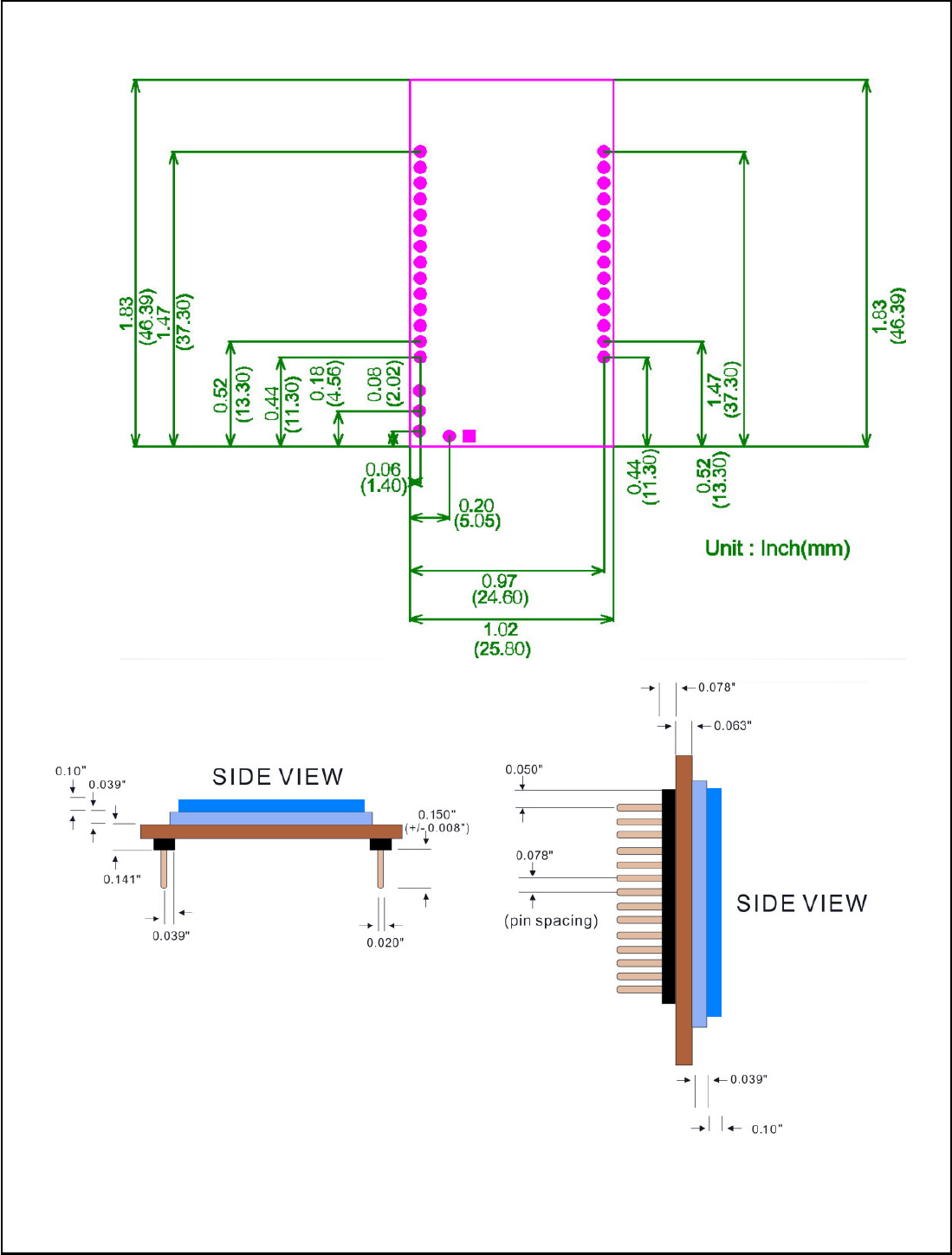
RB540HM(-a/-c) Mechanical Drawing
Note:
Suggested mating female connectors:
1. Through Hole: Samtec P/N. #SQT-114-01-L-S (RoHS)
2. SMT: Samtec P/N. #MMS-114-02-L-SV (RoHS)

23
RB540HM (-a/-c) Interface Signal Definitions
Pin Name Type
Description Voltage Range
1
NC
-
-
-
2 KEY No Pin
This Pin has been removed. Add a
key to the mating connector to prevent
the module from being
plugged in backwards.
-
3 PIO2 I High to shutdown amplifier circuit
to save power consumption
Vih: 0.625 VDD – VDD + 0.3V
Vil: -0.3V - 0.25 VDD
4 PIO3 I High to put speaker in quiescent
mode
Vih: 0.625 VDD – VDD + 0.3V
Vil: -0.3V -0.25 VDD
5 LINEIN_DET I
High indicates Audio Line thru
JK1 stereo jack. Low is Bluetooth
supported
audio
Vih: 0.625 VDD – VDD + 0.3V
Vil: -0.3V -0.25 VDD
6 VOL+ I High to increase volume Vih: 0.625 VDD – VDD + 0.3V
Vil: -0.3V -0.25 VDD
7 MUTE I Low to mute system Vih: 0.625 VDD – VDD + 0.3V
Vil: -0.3V -0.25 VDD
8 CALL_END I High to End Call Vih: 0.625 VDD – VDD + 0.3V
Vil: -0.3V -0.25 VDD
9 BAT_CHECK I Battery Check Vih: 0.625 VDD – VDD + 0.3V
Vil: -0.3V -0.25 VDD
10 VOL- I High to decrease volume Vih: 0.625 VDD – VDD + 0.3V
Vil: -0.3V -0.25 VDD
11 SPI_MOSI I SPI Signal, MOSI Vih: 0.625 VDD – VDD + 0.3V
Vil: -0.3V -0.25VDD
12 SPI_CLK I SPI Signal, CLK Vih: 0.625 VDD – VDD + 0.3V
Vil: -0.3V -0.25 VDD
13 SPI_CS I SPI Signal, CS Vih: 0.625 VDD – VDD + 0.3V
Vil: -0.3V -0.25 VDD
14 SPI_MISO O SPI Signal, MISO Voh: 0.75VDD – VDD
Vol: 0 – 0.125V
15 PIO8 O Active Low, LED 4 Voh: 0.75VDD – VDD
Vol: 0 – 0.125V
16 PIO4 O Active Low, LED 3 Voh: 0.7 5VDD – VDD
Vol: 0 – 0.125V
17
3V3
P
3
.
3V
VDD: 3
.
1
V
–
3
.
6V
18 GND - Ground
19
VBAT
I
Battery
input
pin
VBAT:
3.3V
–
4.4
V
20 RESET I Active Low, must be low for at
least 5ms
Vih: 0.625 VDD – VDD + 0.3V
Vil: -0.3V – 0.25 VDD
21 LED1 O Active Low, Boot up sequence
indicator2
Voh: 0.75 VDD – VDD
Vol: 0 – 0.125V
22 LED0 O Active Low, Boot up sequence
indicator1
Voh: 0.75 VDD – VDD
Vol: 0 – 0.125V
23 MIC I Microphone Input, input
impedance 6K Ohm. 4mV rms ~ 800mV rms
24
GND
-
GND
25 SPK_L_P O
Speaker output Left Channel,
Up to 2Vpk-pk differential at a load of 16
ohm. Can drive at least
8 ohm speaker directly.
Full scale swing (Differential):
750 mV rms
26 SPK_L_N O
Speaker output Left Channel,
Up to 2Vpk-pk differential at a load of 16
ohm. Can drive at least
8 ohm speaker directly.
Full scale swing (Differential):
750 mV rms
27 SPK_R_N O
Speaker output Right Channel,
Up to 2Vpk-pk differential at a load of 16
ohm. Can drive at least
8 ohm speaker directly.
Full scale swing (Differential):
750 mV rms
28 SPK_R_P O
Speaker output Right Channel,
Up to 2Vpk-pk differential at a load of 16
ohm. Can drive at least
8 ohm speaker directly.
Full scale swing (Differential):
750 mV rms
24
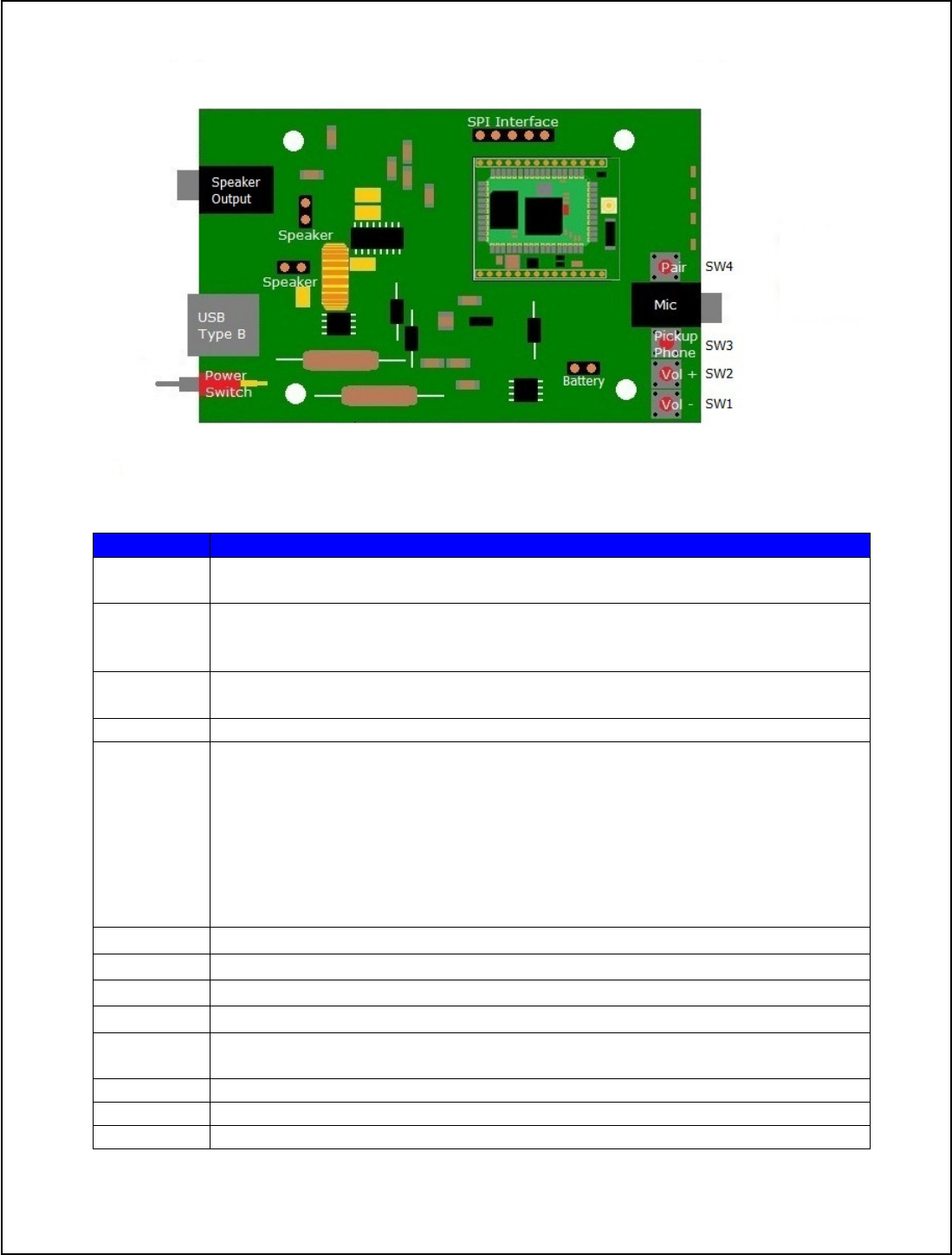
RB540MB Development Board Figure& Functional Descriptions
The RB540MB Development PCB has white silkscreen legend or reference designations located by
the switches and connectors described below.
Switches
Functional Description
PSW1
Power Toggle Switch: This switch controls the power to the RB5
4
0HM module that is
mounted on the RB540MB board. To remove the RB540HM, turn off PSW1.
USB1
USB
-
B Jack Power Source: The development board is power
ed through this USB
interface. When USB power is applied to the RB540MB Development Board, LED 102
will be ON. To turn the power on to the RB540HM, turn on the PSW1 Power Switch.
MIC1A
Stereo Jack Microphone input: Plug in for microphone when using for ha
nd free
phone or headset device.
SPK1
Stereo output Jack: Plug in external speaker to hear audio.
SW4
Pairing / Battery Check
(optional)
Button
a. Pairing function: see each application firmware operations.
b. Battery check function (optional): As soon as this button is pressed, battery
power level will be indicated by amount of LED light up
1 LED ≥ 3.2V, < 3.4V
2 LEDs ≥ 3.4V, < 3.6V
3 LEDs ≥ 3.6V, < 3.8V
4 LEDs ≥ 3.8V
SW3
Call Pick Up / END button
SW2
Volume up button
SW1
Volume down button
JP1
SPI Conne
ction: Use for uploading new firmware and debugging.
BATT1
Battery Input: provide power by battery when not using USB
-
B input power. Do Not
connect both power sources at the same time.
SP
-
L
Left Channel Speaker: directly connect to 4 ohm speaker
.
SP
-
R
R
ight Channel Speaker: directly connect to 4 ohm speaker.
LED 1
–
4
Paring and Battery LEDs.
PSW1
USB1
MIC1A
SPK1
JP1
BATT1
SP-L
SP-R
LED1
L
ED2
LED3
LED4

25
Operating the RB540MB for Standard RX
The RB540-a/c has optional firmware for Standard HFP+A2DP Stereo RX. This firmware allows
the user to establish a Bluetooth stereo connection between a RB540-a/c module and a Bluetooth
capable cell phone. After a Bluetooth connection is established with the phone, the user can pick up
a phone call or play music from his phone.
The following will explain how to use the RB540MB switches to control the RB540-a/c module
with the standard HFP+A2DP RX firmware.
Connect a microphone, speaker and USB cable into RB540MB board.
1. Power ON: After turning on Power Switch PSW1, the LED 1–4 will flash once and light from
LED1 – LED2 – LED3 – LED4, then LED4 – LED3 – LED2 – LED1, then all LED1–4 will
flash for 2 times. If no paired before, the module will automatically start pairing and enter
discoverable mode. If paired before, the module will immediately look for the previously
paired device and try to reconnect. After 5 minutes, no Bluetooth Connection is established, the
module will go to standby mode and the LED1 will flash every 2 seconds.
2. Initiate Pairing: When the module is in standby mode, press button SW4 for 5 seconds to
initiate entering discoverable and pairing. If pressing longer than 10 seconds, the BT module
will clear paired device and look up for new BT device again. During the pairing, LED1–4 will
flash on and off at 0.5 second rate.
Turn on BT mode in your phone, and go to search mode. You can use phone to connect
RB540MB. The device name to search for RB540-a is "Std RX v21.004", and for RB540-c is
“Std RX v22.004”. After paired, LED1–4 will flash 5 times and then LED1 will flash at
1second rate while LED 2-4 off. Once connected, as shown on your phone, you can start to
play music to RB540MB.
3. Play Music: Plug your speakers into the SP-R and SP-L two pin headers or into the SPK1
Stereo Jack. There is no polarity. Go to your phone application and start playing music. There
are 10 levels of volume up and down. SW2 is volume + and SW1 is volume -. It will have a
warning sound when reaching maximum volume. Button SW2 and SW1 can be pressed step
by step or continuously. You can also use phone to change speaker volume.
4. Hands Free Phone Operation (HFP): The RB540MB can also be used for hands free phone.
Use button SW3 for call pick up/ end call, once you hear ring tone from speaker, plug
microphone and speaker for your hand free device.
Incoming call: when incoming call, the 4 LEDs will flash 8 times. It will repeat until the call is
pick up, go to voicemail or disconnect. After pick up call, LED 1-4 will flash from LED1 –
LED2 – LED3 – LED4, then LED4 – LED3 – LED2 – LED1 periodically.
End call: After picking up the call, if press SW3 button will disconnect the call. Music resumes
after call ends.
Power cycle RB540MB or switch off-and-on the cell phone Bluetooth, the module will automatically
connect to the cell phone.

26
Operating the RB540MB for TrueWireless Stereo Sound
The RB540 has optional firmware for True Wireless Stereo sound. This firmware allows the user to
establish a Bluetooth stereo connection between two RB540 Modules and a Bluetooth capable cell
phone. After a Bluetooth connection is established with the phone, then establish a connection
between RB540MB Master and RB540MB Slave. The user can now play music from his phone.
When the RB540MB Master receives the Music from the phone, it will split the sound into two
channels for stereo operation. The RB540MB Master will play one channel and the RB540MB
Slave will play the other channel.
The following will explain how to use the RB540MB switches to control the RB540 module with
the standard TWS firmware.
Connect a speaker and USB cable into both RB540MB boards.
1. Power ON: First we will create a Master RB540. Power on one of the RB540 modules by
plugging in the USB cable and turn on the PSW1.
2. Initiate Pairing with cell phone: Short press SW4 button to enter the Bluetooth discovery mode,
the on-board LED1 should start flashing and a periodic "du" sound can be heard from through
the speaker connected to the Master RB540MB.
Use the cell phone to discover and connect with the Master. The device name to search for is
"TWS v11.003". The LED1 will stay lit after Bluetooth connection is established.
Note: the first RB540 paired to a cell phone is a Master RB540.
3. Initiate Pairing with two RB540: Short press SW2 button on both (Master and Slave) units to
start the pairing process between them. A periodic "du du" sound can be heard through both
speakers and LED2 will be flashing on both units. The first time they pair might take a minute.
This is due to the two Bluetooth modules synchronizing their clocks. Once the pairing process
is complete, the LED2 will stay lit on both RB540MB.
4. Play Music: Use the cell phone to play music. After a short delay, you to hear the music in stereo
through the two speakers. Volume control is available only on cell phone in this firmware.
Note: RB540 Master is SPK_L, and RB540 Slave is SPK_R.
The next time you use the phone to connect, the complete process will only take a couple of seconds.
Use the cell phone to reconnect “TWS v11.003”, the modules will automatically connect to each
other and the music can be played immediately.
Note: Long press 3 seconds on either SW2 or SW4 will trigger a “reset” on RB540. Pairing
information will be cleared in RB540. Due to different cell phone behavior, some cell phone
may be able to reconnect to RB540 after a “reset” because the cell phone still keep the pairing
record with RB540.

27
Operating the RB540MB for Tx/RX (two-way SCO Link)
The RB540 has optional firmware for TX/RX (two-way SCO Link). This firmware allows the user
to establish a Bluetooth proprietary connection between two RB540 Modules. After a Bluetooth
connection is established between two RB540MB, the user can use the modules as two-way TX/RX
communication.
The following will explain how to use the RB540MB switches to control the RB540 module with
the standard TX/RX (two-way SCO Link) firmware.
Connect a microphone, speaker and USB cable into both RB540MB boards.
1. Power ON RX: Plug your speakers into the SP-R and SP-L two pin headers or into the SPK1
Stereo Jack. There is no polarity. Turn on the PSW1 on the RB540 RX module. All 4 LEDs
will flash once, then LED 1–4 will flash from LED1 – LED2– LED3 – LED4, then LED4–
LED3 – LED2 – LED1. All 4 LEDs will flash at 1second rate. At this moment, the BT module
enters discoverable mode and starts pairing.
2. Power ON TX: Plug your speakers into the SPK1 Stereo Jack. Turn on the PSW1 on the
RB540 TX module. LED1-2 will quick flash alternately, LED3 stays lit.
3. Initiate Pairing: Press TX SW4 to start discovery and pairing. LED2 will quick flash, LED3
remains lit. Wait until RX LED1 is on, press TX SW3 to connect to RX. After connected, RX
LED1 will flash at 1second rate. TX LED2 will flash 2 times a second, LED3 stays lit.
Two-way communication is available on TX and RX.
Both TX and RX can speak and listen to each other synchronously.
Power cycle RB540MB TX or RX, need to repeat #3 Initiate Pairing process to establish the connection.
There is no auto-reconnection supported in this firmware revision.
Note: If RX has paired to another host device (ex. smart phone), please make sure you clear the
previous pairing record before reconnecting to TX. Long press RX SW4 for 12 seconds to
clear the previous pairing record.

28
Operating the RB540MB for Tx/RX (one-way A2DP)
The RB540 has optional firmware for TX/RX (one-way A2DP). This firmware allows the user to
establish a Bluetooth proprietary connection between two RB540 Modules. After a Bluetooth
connection is established between two RB540MB, the user can use the modules as one-way TX/RX
communication.
The following will explain how to use the RB540MB switches to control the RB540 module with
the standard TX/RX (one-way A2DP) firmware.
Connect an USB cable into both RB540MB boards.
1. Power ON RX: Plug your speakers into the SPK1 Stereo Jack. Turn on the PSW1 on
RB540MB RX. A “du-du-du” sound will play for power on indication. LED1-2 will flash
alternately, LED4 stays lit. RB540 RX will automatically enter discoverable mode at all times.
2. Power ON TX and initiate Pairing: Plug the microphone into MIC1A. Turn on the PSW1 on
RB540MB TX. LED1-2 will flash alternately, LED4 stays lit. In first 10 seconds, RB540 TX
will try to connect to last paired RX, the reconnection will be established in couple seconds. If
no reconnection established in 10 seconds, RB540 TX will automatically enter pairing mode to
search a new RX. After paired, a “du-du” sound will play in RX, and LED1, LED4 will lit on
both TX and RX RB540MB boards.
Note: Suggested always to power on RX first, in order to shorten TX pairing time.
3. Now you can use TX as talking or music source, and hear the sound from RX.
4. Volume change on TX: There are 21 levels of volume up and down on TX. SW2 is volume +
and SW1 is volume -. Button SW2 and SW1 can be pressed step by step or continuously.
Note: Volume change function not supported in RX.
5. Clear Pairing Record: Long press TX SW4 for 10 seconds to clear the previous pairing record.
Note:
1. Power cycle RB540MB RX, the module will automatically enter discoverable mode for any
available TX in the range.
2. Power cycle RB540MB TX, the module will first try to connect to last paired RX for 10
seconds, if no connection established in 10 seconds, TX will automatically enter pairing
mode for searching a new RX.
3. No pairing button needed in this firmware revision, all pairing connection will be
automatically handled in couple seconds.
29
Upgrading the Firmware in the RB540 series
Use JP1 connector on the RB540MB with the SPI cable and Bluesuite software to
upgrade the firmware. Radicom will provide the Bluesuite software and SPI cable for the
firmware upgrade. To upload new firmware to the RB540 series module or RB540HM,
use the SPI pins and follow the procedure below.
1. The following 3 items are required to update firmware:
a. Windows XP or Windows 7 machine with printer port
b. SPI cable
c. Bluesuite 2.4.8 Software
2. Install Bluesuite 2.4.8 in the computer.
3. Connect SPI cable 25pin connector to the computer printer port. Connect the 5pin
connector to JP1 5pin header on the RB540MB. Make sure the polarity of 5pin
header is correctly inserted into JP1 on the RB540. The white mark on the 5pin
connector of the SPI cable is pin 1. The pin 1of the JP1 connector can be identified
by the pin closest to the JP1 Silkscreen or by the square pad on the bottom side of
the PCB.
4. Turn on the Power Switch on the RB540MB.
5. In Windows XP machine, Start > All Program > CSR BlueSuite 2.4.8 > Blueflash.
6. Click “Stop processor”, then browse and choose the new firmware file.
7. Click “Download file” to update firmware.
8. After download, click “start processor”.
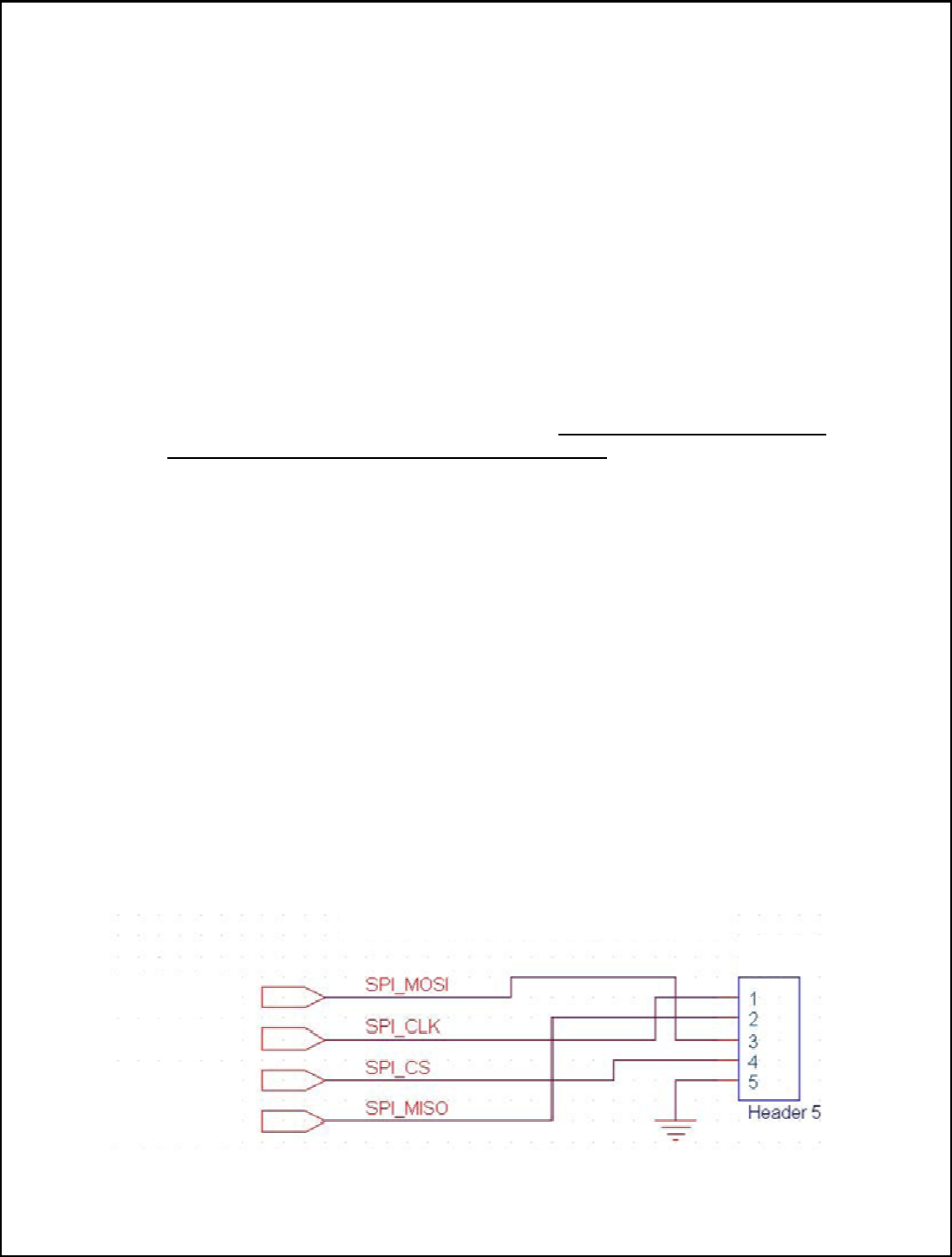
SPI Programming Connector (JP1)
RB540 SPI programming connector
RB540 pin20
RB540 pin21
RB540 pin22
RB540 pin23
JP1

30
Suggested Microphone Circuit
Suggested Differential to Single End Circuit
Suggested LED Circuit

31
Limited Warranty
Warranty Coverage and Duration
Radicom Research, Inc. (“RRI”) warrants to the original purchaser its RRI-manufactured
products (“Product”) against defects in material and workmanship under normal use and
service for a period of one year from the date of delivery.
During the applicable warranty period, at no charge, RRI will, at its option, either repair,
replace or refund the purchase price of this Product, provided it is returned in accordance
with the terms of this warranty to RRI. Repair, at the option of RRI, may include the
replacement of parts, boards or other components with functionally equivalent
reconditioned or new parts, boards or other components. Replaced parts, boards or other
components are warranted for the balance of the original applicable warranty period. All
replaced items shall become the property of RRI.
RRI MAKES NO GUARANTEE OR WARRANTY THAT THE PRODUCT WILL
PREVENT OCCURRENCES, OR THE CONSEQUENCES THEREOF, WHICH THE
PRODUCT IS DESIGNED TO DETECT.
This expressed limited warranty is extended by RRI to the original end-user purchaser
only, and is not assignable or transferable to any other party. This is the complete
warranty for the Product manufactured by RRI, and RRI assumes no obligation or
liability for additions or modifications to this warranty. In no case does RRI warrant the
installation, maintenance or service of the Product.
RRI is not responsible in any way for any ancillary equipment not furnished by RRI that is
attached to or used in connection with the Product, or for operation of the Product with
any ancillary equipment, and all such equipment is expressly excluded from this warranty.
Because of wide variations in topographical and atmospheric conditions,
which may require availability of repeater stations or of particular radio frequencies, RRI
assumes no liability for range, coverage or suitability of the Product for any particular
application. Buyer acknowledges that RRI does not know a particular purpose for which
buyer wants the product, and that buyer is not relying on RRI’s skill and judgment to
select or furnish suitable goods.
What this Warranty does NOT Cover:
(a) Defects or damage resulting from use of the Product in other than its normal and
customary manner.
(b) Defects or damage from misuse, accident or neglect.
(c) Defects of damage from improper testing, operation, maintenance, installation,
alteration, modification or adjustment.
(d) Disassembly or repair of the Product in such a manner as to adversely affect
performance or prevent adequate inspection and testing to verify any warranty claim.
(e) Any Product that has had its serial number or date code removed or made illegible.

32
How to Receive Warranty Service:
To obtain warranty service, contact RRI by phone +886-2-2664-9168 for your sales
representative or email to sales@radi.com for an RMA (Return Merchandise
Authorization) number. Deliver or send the Product, transportation and insurance prepaid
to RRI, with the RMA number clearly marked on the outside of the package.
General Provision
This warranty sets forth the full extent of RRI’s responsibilities regarding the Product.
Repair, replacement or refund of the purchase price, at RRI’s option, is the exclusive
remedy.
THIS WARRANTY IS GIVEN IN LIEU OF ALL OTHER EXPRESSED
WARRANTIES. ANY APPLICABLE IMPLIED WARRANTIES, INCLUDING
WITHOUT LIMITATION, THE IMPLIED WARRANTY OF MERCHANTABILITY,
ARE LIMITED TO THE DURATION OF THIS LIMITED WARRANTY. TO THE
FULLEST EXTENT PERMITTED BY LAW, RRI DISCLAIMS ANY LIABILITY
FOR DAMAGES IN EXCESS OF THE PURCHASE PRICE OF THE PRODUCT, FOR
ANY LOSS OF USE, LOSS OF TIME, INCONVENIENCE, COMMERCIAL LOSS,
LOST PROFITS OR SAVING OR OTHER INCIDENTAL, SPECIAL OR
CONSEQUENTIAL DAMAGES ARISING OUT OF THE USE OR INABILITY TO
USE OR FAILURE OF SUCH PRODUCT.

33
Contacting Radicom Research, Inc.
If more information or technical support is needed, please contact us:
2148 Bering Drive
San Jose, CA. 95131
Telephone: (408) 383 9006
Fax: (408) 383 9007
or
e-mail: sales@radi.com
http://www.radi.com/