Renesas R61509V Users Manual ER61509V_0.11_20080424
R61509V R61509V
R61509V to the manual a8ca65a3-9abb-45fc-9ff1-2a1acc3f8dcb
2015-02-06
: Renesas Renesas-R61509V-Users-Manual-523436 renesas-r61509v-users-manual-523436 renesas pdf
Open the PDF directly: View PDF ![]() .
.
Page Count: 181 [warning: Documents this large are best viewed by clicking the View PDF Link!]
Rev. 0.11 April 25, 2008, page 1 of 181
Target Spec
R61509V
260k-color, 240RGB x 432-dot graphics liquid crystal
controller driver for Amorphous-Silicon TFT Panel
REJxxxxxxx-xxxx
Rev.0.11
April 25, 2008
Description ......................................................................................................... 6
Features ......................................................................................................... 7
Power Supply Specifications .............................................................................. 8
Differences Between R61509 and R61509V...................................................... 9
Block Diagram.................................................................................................... 10
Block Function.................................................................................................... 11
1. System Interface.....................................................................................................................................................11
2. External Display Interface (RGB, VSYNC interfaces)........................................................................................12
3. Address Counter (AC) ...........................................................................................................................................12
4. Graphics RAM (GRAM)........................................................................................................................................13
5. Grayscale Voltage Generating Circuit..................................................................................................................13
6. Liquid Crystal Drive Power Supply Circuit..........................................................................................................13
7. Timing Generator ..................................................................................................................................................13
8. Oscillator (OSC).....................................................................................................................................................13
9. Liquid crystal driver Circuit ..................................................................................................................................13
10. Internal Logic Power Supply Regulator...............................................................................................................13
Pin Function........................................................................................................ 14
Pad Arrangement ................................................................................................ 19
Pad coordinate..................................................................................................... 21
Bump Arrangement............................................................................................. 36
Connection Example........................................................................................... 37
GRAM Address Map .......................................................................................... 38
Instruction ......................................................................................................... 40

R61509V Target Spec
Rev. 0.11 April 25, 2008, page 2 of 181
Outline ..........................................................................................................................................................................40
Instruction Data Format..............................................................................................................................................40
Index (IR) .....................................................................................................................................................................41
Display control .............................................................................................................................................................41
Device code read (R000h) ......................................................................................................................................41
Driver Output Control (R001h)..............................................................................................................................41
LCD Drive Wave Control (R002h).........................................................................................................................42
Entry Mode (R003h) ...............................................................................................................................................42
Display Control 1 (R007h) .....................................................................................................................................45
Display Control 2 (R008h) .....................................................................................................................................46
Display Control 3 (R009h) .....................................................................................................................................48
8 Color Control (R00Bh)........................................................................................................................................49
External Display Interface Control 1 (R00Ch)......................................................................................................50
External Display Interface Control 2 (R00Fh) ......................................................................................................52
Panel Interface Control 1 (R010h).........................................................................................................................53
Panel Interface Control 2 (R011h).........................................................................................................................55
Panel Interface Control 3 (R012h).........................................................................................................................56
Panel Interface Control 4 (R013h).........................................................................................................................58
Panel Interface Control 5 (R014h).........................................................................................................................59
Panel Interface Control 6 (R020h).........................................................................................................................60
Panel Interface Control 7 (R021h).........................................................................................................................62
Panel Interface Control 8 (R022h).........................................................................................................................63
Panel Interface Control 9 (R023h).........................................................................................................................65
Frame Marker Control (R090h).............................................................................................................................66
Power Control...............................................................................................................................................................67
Power Control 1 (R100h) .......................................................................................................................................67
Power Control 2 (R101h) .......................................................................................................................................69
Power Control3 (R102h) ........................................................................................................................................73
Power Control 4 (R103h) .......................................................................................................................................74
RAM Access..................................................................................................................................................................75
RAM Address Set (Horizontal Address) (R200h) RAM Address Set (Vertical Address) (R201h) ........................75
GRAM Data Write (R202h) ....................................................................................................................................76
GRAM Data Read (R202h).....................................................................................................................................77
NVM Data Read / NVM Data Write (R280h).........................................................................................................78
Window Address Control .............................................................................................................................................81
Window Horizontal RAM Address Start (R210h), Window Horizontal RAM Address End (R211h) ...................81
Window Vertical RAM Address Start (R212h), Window Vertical RAM Address End (R213h) ............................81
γ Control .......................................................................................................................................................................82
γ Control 1 ~ 14 (R300h to R309h) ........................................................................................................................82
Base Image Display Control........................................................................................................................................84
Base Image Number of Line (R400h) .....................................................................................................................84
Base Image Display Control (R401h) ....................................................................................................................84
Base Image Vertical Scroll Control (R404h) .........................................................................................................84
Partial Display Control ................................................................................................................................................88
Partial Image 1: Display Position (R500h), RAM Address 1 (Start Line Address) (R501h), RAM Address 1 (End Line Address)
(R502h) ................................................................................................................................................................88
Pin Control ...................................................................................................................................................................89
Test Register (Software Reset) (R600h) .................................................................................................................89

R61509V Target Spec
Rev. 0.11 April 25, 2008, page 3 of 181
NVM Control ................................................................................................................................................................90
NVM Access Control 1 (R6F0h), NVM Access Control 2 (R6F1h), NVM Access Control 3 (R6F2h) .................90
Instruction List.................................................................................................... 92
Reset Function .................................................................................................... 93
Basic Mode Operation of the R61509V.............................................................. 95
Interface and Data Format .................................................................................. 96
System Interface.................................................................................................. 99
80-System 18-bit Bus Interface ...................................................................................................................................100
80-System 16-bit Bus Interface ...................................................................................................................................101
80-System 9-bit Bus Interface .....................................................................................................................................104
Data Transfer Synchronization in 9-bit Bus Interface Operation ............................................................................105
80-System 8-bit Bus Interface .....................................................................................................................................106
Serial Interface.............................................................................................................................................................109
VSYNC Interface................................................................................................ 112
Notes to VSYNC Interface Operation .........................................................................................................................114
FMARK Interface ............................................................................................... 116
FMP Setting Example..................................................................................................................................................120
RGB Interface ..................................................................................................... 121
RGB Interface ..............................................................................................................................................................121
Polarities of VSYNCX, HSYNCX, ENABLE, and DOTCLK Signals.......................................................................122
Setting Example of Display Control Clock in RGB Interface Operation .................................................................123
RGB Interface Timing .................................................................................................................................................124
16-/18-Bit RGB Interface Timing...........................................................................................................................124
RAM access via system interface in RGB interface operation ..................................................................................125
16-Bit RGB Interface ...................................................................................................................................................126
18-bit RGB Interface....................................................................................................................................................127
Notes to RGB Interface Operation..............................................................................................................................128
RAM Address and Display Position on the Panel .............................................. 129
Instruction Setting Example........................................................................................................................................132
Window Address Function ................................................................................. 134
Scan Mode Setting .............................................................................................. 135
8-Color Display Mode ........................................................................................ 136
Frame-Frequency Adjustment Function ............................................................. 137
Relationship between Liquid Crystal Drive Duty and Frame Frequency.................................................................137

R61509V Target Spec
Rev. 0.11 April 25, 2008, page 4 of 181
Partial Display Function ..................................................................................... 139
Liquid Crystal Panel Interface Timing ............................................................... 140
Internal Clock Operation.............................................................................................................................................140
RGB Interface Operation.............................................................................................................................................141
γ Correction Function.......................................................................................... 142
γ
Correction Function..................................................................................................................................................142
γ
Correction Circuit......................................................................................................................................................142
γ
Correction Registers ..................................................................................................................................................143
Reference level adjustment registers ...........................................................................................................................143
Interpolation Registers.................................................................................................................................................145
Frame Memory Data and the Grayscale Voltage.......................................................................................................148
Power Supply Generating Circuit ....................................................................... 149
Power Supply Circuit Connection Example 1 (VCI1 = VCIOUT)............................................................................149
Power Supply Circuit Connection Example 2 (VCI1 = VCI Direct Input)...............................................................150
Specifications of Power-supply Circuit External Elements................................ 151
Voltage Setting Pattern Diagram ........................................................................ 152
Liquid Crystal Application Voltage Waveform and Electrical Potential ..................................................................153
VCOMH and VREG1OUT Voltage Adjustment Sequence ............................... 154
NVM Control...................................................................................................... 155
NVM Load (Register Resetting) Sequence .................................................................................................................156
NVM Write Sequence...................................................................................................................................................157
NVM Erase Sequence ..................................................................................................................................................158
Power Supply Setting Sequence ......................................................................... 159
Notes to Power Supply ON Sequence ................................................................ 161
Instruction Setting Sequence and Refresh Sequence .......................................... 162
Display ON/OFF Sequences and Refresh Sequence .................................................................................................162
Shutdown Mode Sequences .........................................................................................................................................163
Partial Display Setting .................................................................................................................................................166
Absolute Maximum Ratings ............................................................................... 167
Electrical Characteristics .................................................................................... 168
DC Characteristics .......................................................................................................................................................168
Step-up Circuit Characteristics..............................................................................................................................170
Internal Reference Voltage: Condition ..................................................................................................................170
Power Supply Voltage Range .................................................................................................................................171
Output Voltage Range ............................................................................................................................................171
AC Characteristics .......................................................................................................................................................172

R61509V Target Spec
Rev. 0.11 April 25, 2008, page 5 of 181
Clock Characteristics .............................................................................................................................................172
80-system 18-/16-/9-/8-bit Bus interface Timing Characteristics .........................................................................172
Clock Synchronous Serial Interface Timing Characteristics.................................................................................173
RGB Interface Timing Characteristics...................................................................................................................173
LCD Driver Output Characteristics.......................................................................................................................174
Reset Timing Characteristics .................................................................................................................................174
Notes to Electrical Characteristics ..............................................................................................................................175
Test Circuits..................................................................................................................................................................176
Timing Characteristics.................................................................................................................................................177
80-system Bus Interface..........................................................................................................................................177
Clock Synchronous Serial Interface .......................................................................................................................178
Reset Operation ......................................................................................................................................................178
LCD Driver and VCOM Output Characteristics ...................................................................................................179

R61509V Target Spec
Rev. 0.11 April 25, 2008, page 6 of 181
Description
The R61509V is a single-chip liquid crystal controller driver LSI for a-Si TFT panel, incorporating RAM
for a maximum 240 RGB x 432 dot graphics display, gate driver, source driver and power supply circuits.
For efficient data transfer, the R61509V supports high-speed interface via 8-/9-/16-/18-bit ports as system
interface to the microcomputer. As moving picture interface, the R61509V also supports RGB interface
(VSYNCX, HSYNCX, DOTCLK, ENABLE and DB17-0).
The power supply circuit incorporates step-up circuit and voltage follower circuit to generate TFT liquid
crystal panel drive voltages.
The R61509V’s power management functions such as 8-color display and shut down and so on make this
LSI an ideal driver for the medium or small sized portable products with color display systems such as
digital cellular phones or small PDAs, where long battery life is a major concern.

R61509V Target Spec
Rev. 0.11 April 25, 2008, page 7 of 181
Features
• A single-chip controller driver incorporating a gate circuit and a power supply circuit for a maximum
240RGB x 432dots graphics display on amorphous TFT panel in 262k colors
• System interface
– High-speed interfaces via 8-, 9-, 16-, 18-bit parallel ports
– Clock synchronous serial interface
• Moving picture display interface
– 16-/18-bit RGB interface (VSYNCX, HSYNCX, DOTCLK, ENABLE, DB17-0)
– VSYNC interface (System interface + VSYNCX)
– FMARK interface (System interface + FMARK)
• Window address function to specify a rectangular area in the internal RAM to write data
• Write data within a rectangular area in the internal RAM via moving picture interface
– Reduce data transfer by specifying the area in the RAM to rewrite data
– Enable displaying the data in the still picture RAM area with a moving picture simultaneously
• Abundant color display and drawing functions
– Programmable for 262k-color display
– Partial display function
• Low -power consumption architecture (allowing direct input of interface I/O power supply)
– Shut down function
– 8-color display function
Input power supply voltages: IOVCC (interface I/O power supply)
VCC (logic regulator power supply)
VCI (liquid crystal analog circuit power supply)
• Incorporates a liquid crystal drive power supply circuit
– Source driver liquid crystal drive/VCOM power supply: DDVDH
VCL
– Gate drive power supply: VGH
VGL
– VCOM drive (VCOM power supply): VCOMH
VCOML
• Liquid crystal power supply startup sequencer
• TFT storage capacitance: Cst only (common VCOM formula)
• 233,280-byte internal RAM
• Internal 720-channel source driver and 432-channel gate driver
• Single-chip solution for COG module with the arrangement of gate circuits on both sides of the glass
substrate
• Internal NVM
User identification code: 8 bits
VCOM level adjustment: 7 bits x 2. Rewriting is available up to 5 times
R61509V Target Spec
Rev. 0.11 April 25, 2008, page 8 of 181
Power Supply Specifications
Table 1
No. Item R61509V
1 TFT data lines 720 output
2 TFT gate lines 432 output
3 TFT display storage capacitance Cst only (Common VCOM formula)
S1~S720 V0 ~ V63 grayscales
G1~G432 VGH-VGL
4 Liquid crystal
drive output
VCOM Change VCOMH-VCOML amplitude with electronic volume
Change VCOMH with either electronic volume or from
VCOMR
IOVCC
(interface voltage)
1.65V ~ 3.3V
Power supply to IM0_ID, IM1-2, RESETX, DB17-0, RDX,
SDI, SDO, WR_SCL, RS, CSX, VSYNCX, HSYNCX,
DOTCLK, ENABLE, FMARK
Connect to VCC and VCI on the FPC when the electrical
potentials are the same.
VCC
(logic regulator power
supply)
2.5V ~ 3.3V
Connect to IOVCC and VCI on the FPC when the electrical
potentials are the same.
5 Input voltage
VCI
(liquid crystal drive
power supply voltage)
2.5V ~ 3.3V
Connect to IOVCC and VCC on the FPC when the electrical
potentials are the same.
DDVDH 4.5 ~ 6.0V (VCI1 x 2)
VGH 10 ~ 18.0 V (VCI1 x 5, 6)
VGL -4.5 ~ -13.5V (VCI1 x –3, -4, -5)
VGH-VGL max. 28V
VCL -1.9 ~ -3.0V (VCI1 x -1)
6 Liquid crystal
drive
voltages
VCI-VCL max. 6V
See “DC characteristics” in Chapter “Electrical Characteristics” for voltage spec.
Difference Between R61509 and R61509V 2008.04.18
Index Command Code Function R61509 R61509V
(Pin) System Interface IM2-0=011, TRI=1, DFM=0 8bit 3 transfer (2bit-8bit-8bit) Supported Deleted
R000h Device Code Read 1509H B509H
R002h LCD Drive Waveform Control NW[1-0] --> NW bit is deleted. 1, 2, 3 or 4 line inversion 1 line inversion
R003h Entry Mode HWM High Speed RAM Write Supported Deleted
EPF[1-0]
Sets data format when writing 16bit
data in 18bit format. Supported Deleted
R006h Outline Sharpening Control EGMODE, AVST[2:0], ADST[2:0]DTHU[1:0], DTHL[1:0] Outline Sharpening Function Supported Deleted
R007h Display Control 1 PTDE[1-0]-->PTDE0 Controls partial image 1 and 2. Partial image 1 and 2 Partial image 1
VON Starts VCOM output Manual setting
Deleted. (Because the sequence is changed. See "Power Supply
Setting Sequence" for detail. )
GON Sets gate output to OFF level. Manual setting
Deleted. (Because the sequence is changed. See "Power Supply
Setting Sequence" for detail. )
DTE Starts gate scan Manual setting
Deleted. (Because the sequence is changed. See "Power Supply
Setting Sequence" for detail. )
D[1-0] Starts/halts display operation Manual setting
Deleted. (Because the sequence is changed. See "Power Supply
Setting Sequence" for detail. )
R008h Display Control 2 FP[3-0] Defines front porch 2-14 lines (in units of 1 line) 3-128 lines (in units of 1 line)
BP[3-0] Defines back porch 2-14 lines (in units of 1 line) 3-128 lines (in units of 1 line)
R009h Display Control 3 PTG[1-0] --> Deleted. Sets gate scan mode Normal scan / interval scan Normal scan only (Interval scan is not available)
ISC[3:0] Sets gate scan cycle 3, 5, 7, 9, 11, 13 or 15 frames Deleted
PTS[2-0] -->PTS Sets source output level V0-V31 V0-V63
R00Bh Low Power Control VEM[0] --> VEM[1-0] Execute VCOM equalize. VCOMH to VCOML only VCOML to VCOMH / VCOMH to VCOML (See description)
R00Ch External Display Interface Control RIM[1-0]=10
Selects 6bit 3 transfer via RGB
interface Supported Deleted
R012h Panel Interface Control 3 VEQWI[1-0]-->VEQWI[2-0] Defines VCOM equalize period. 0, 1, 2 or 3 clock period 0, 1, 2, 3, 4, 5, 6 or 7 clock period
R020h Panel Interface Control 4 RTNE[6-0]-->RTNE[5-0] Defines number of clock per line. 16-127 clocks 16 - 63 clocks
R021h Panel Interface Control 5 NOWE[3-0]-->NOWE[2-0] Defines gate non overlap period. 0 - 15 clocks 0 - 7 clocks
SDTE[3-0]-->SDTE[2-0] Defines source output delay period. 0 - 15 clocks 0 - 7 clocks
R092h MDDI Sub-display Control SIM[1:0] --> Deleted.
Defines data format for sub display
interface operation. Supported Deleted
R100h Power Control 1 SAP[1-0]
Adjusts bias current in source
amplifier. Supported
Deleted. (Because the sequence is changed. See "Power Supply
Setting Sequence" for detail. )
SAP --> SOAPON Enables source amplifier Supported
Deleted. (Because the sequence is changed. See "Power Supply
Setting Sequence" for detail. )
BT[2-0] Defines step-up factor DDVDH: x2, VCL:x-1, VGH: x6, x7, VGL: x-3, x-4, x-5 DDVDH: x2, VCL: x-1, VGH: x5, x6, VGL: x-3, x-4, x-5
APE --> Deleted. Enables power supply circuit Supported
Deleted. (Because the sequence is changed. See "Power Supply
Setting Sequence" for detail. )
SLP --> Deleted. Selects sleep mode. Supported Deleted
R101h Power Control 2 DC1[2-0] Defines step-up factor for DCDC1. Not synchronized with internal clock (Default) Synchronized with internal clock (Default)
DC2[2-0] Defines step-up factor for DCDC2. Not synchronized with internal clock (Default) Synchronized with internal clock (Default)
R102h Power Control 3 VRH[3-0] Sets a factor to generate 4bit (VRH [3:0]) 5bit (VRH [4:0]). Enables minute setting.
VRG1R --> Deleted.
Defines reference level to generate
VREG1OUT Selects external or internal reference voltage. Internal reference voltage only
R103h Power Control 4 VCOMG Defines VCOM amplitude VCOML can be set at GND level Deleted
R110h Power Control 6 PSE Enables power supply sequencer Supported
Deleted. (Because the sequence is changed. See "Power Supply
Setting Sequence" for detail. )
R112h Power Control 7 TBT[1-0] Used in power supply sequencer Supported
Deleted. (Because the sequence is changed. See "Power Supply
Setting Sequence" for detail. )
R280h NVM Data Read / NVM Data Write UID[3:0] User code UID[3:0] VCM[6-0] UID[7-0]
R281h VCOM High Voltage 1 VCM1[4-0] Defines VCOMH 1level VCM1[4-0] NVM specification changed. VCM bit is moved to R280h.
R282h VCOM High Voltage 2 VCMSEL , VCM2[4-0] Defines VCOMH 2level VCMSEL VCM2
Deleted. (Because the R61509V supports both NVM write and erase
functions).
R300h-R309h Gamma Control Gamma Control Gamma control method changed. 84 bit 100 bit (New gamma correction method)
R400h Base Image Number of Line NL0[5-0] Specifies LCD drive line. 16 - 432 line (in units of 8 lines) 240 - 432 lines (in units of 8 lines)
R401h Base Image Display Control NDL0
Defines source output level in non-lit
display area V31-V0 V63-V0
REV0
Inverts grayscale level in the display
area V31-V0 V63-V0
R503h-R505h Partial Image Control PTDP1[8-0] PTSA1[8-0] PTEA1[8-0] --> Deleted. Settings for partial image 2. Partial image 1 and 2 Partial image 1 only
R600h Software Reset SRST--> TRSR Software Reset Software Reset Only secret test registers are initialized.
R606h i80-I/F Endian Control TCREV[1] , TCREV[0] Selects the order of receiving data. Supported Deleted
See each register's description for detail.
R61509V Target Spec
Rev. 0.11 April 25, 2008, page 10 of 181
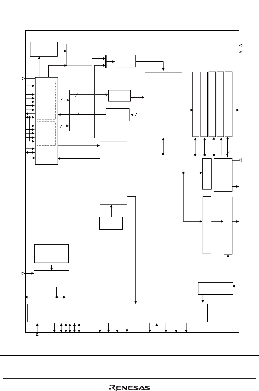
Block Diagram
㩷
㩷
㩷
㩷
㩷
㩷
㩷
㩷
㩷
㩷
㩷
㩷
㩷
㩷
㩷
㩷 㩷
㩷
㩷
㩷
㩷
㩷
㩷
㩷
VCC
VDD
㩷
㩷
㩷
㩷
C13P/C13M
G1-G432
VGH
VGL
㩷 㩷
㩷
㩷
㩷
㩷
㩷
㩷
㩷
㩷
㩷
㩷
㩷
㩷
VMON
VGS
VCI
VCI1
C11P/C11M
C12P/C12M
DDVDH
C21P/C21M
C22P/C22M
GND
A
GND
V63-0
㩷
VREG1OUT
VCOMH
VCOML
VCOMR
VCOM
㩷
㩷
㩷
㩷
㩷
㩷
㩷
㩷
㩷
CSX
RS
WR_SCL
RDX
SDI
SDO
DB17-0
VSYNCX
HSYNCX
DOTCL
K
ENABLE
RESETX
FMAR
K
IOVCC
18
18
㩷
㩷
㩷
㩷
18
18
18
18
VPP1,
VPP3A,3B
IM2-1, IM0_ID
VCL
PROTECT
Index
Register (IR) Control
Register
(CR) Address
Counter
Graphic RAM
(GRAM)
233,280byte
Write data
latch
Read data
latch
System
interface
18 bit
16 bit
9 bit
8 bit
Serial
External
display
interface
Timing
generator
Oscillator
Internal reference
voltage generating
circuit
Internal logic
power supply
circuit
LCD drive level generating circuit
Latch circuit
Latch circuit
M alternation
Latch Circuit
Source line drive circuit
Grayscale voltage
generating circuit
Gamma
correction circuit
Gate line drive circuit
Scan data generating circuit
NVM
Figure 1
R61509V Target Spec
Rev. 0.11 April 25, 2008, page 11 of 181
Block Function
1. System Interface
The R61509V supports 80-system high-speed interface via 8-, 9-, 16-, 18-bit parallel ports and a clock
synchronous serial interface. The interface is selected by setting the IM2-0 pins.
The R61509V has 16-bit index register (IR), 18-bit write-data register (WDR), and 18-bit read-data register
(RDR). The IR is the register to store index information from control register and internal GRAM. The
WDR is the register to temporarily store write data to control register and internal GRAM. The RDR is the
register to temporarily store the read data from the GRAM. The write data from the host processor to the
internal GRAM is first written to the WDR and then automatically written to the internal GRAM by
internal operation. The data is read via RDR from the internal GRAM. Therefore, invalid data is sent to
the data bus when the R61509V performs the first read operation from the internal GRAM. Valid data is
read out when the R61509V performs the second and subsequent read operation.
The R61509V allows writing instructions consecutively by executing the instruction in the same cycle
when it is written (0 instruction cycle).
Table 2 Register Selection (80-System 8-/9-/16-/18-Bit Parallel Interface)
WRX RDX RS Function
0 1 0 Write index to IR
1 0 0 Setting disabled
0 1 1 Write to control register or internal GRAM via WDR
1 0 1 Read from internal GRAM and register via RDR
Table 3 Register Selection (Clock Synchronous Serial Interface)
Start byte
R/W RS Function
0 0 Write index to IR
1 0 Setting disabled
0 1 Write to control register or internal GRAM via WDR
1 1 Read from internal GRAM and register via RDR

R61509V Target Spec
Rev. 0.11 April 25, 2008, page 12 of 181
Table 4
IM2 IM1 IM0 System interface DB pins RAM write data Instruction write
transfer
0 0 0 80-system 18-bit
interface DB17-0 Single transfer (18 bits) Single transfer
(16 bits)
0 0 1 80-system 9-bit
interface DB17-9 2-transfer (1st: 9 bits, 2nd: 9 bits)
2-transfer
(1st: 8 bits, 2nd: 8
bits)
0 1 0 80-system 16-bit
interface
DB17-10,
DB8-1
Single transfer (16 bits)
2-transfer (1st: 2 bits, 2nd: 16 bits)
2-transfer (1st: 16 bits, 2nd: 2 bits)
Single transfer
(16 bits)
0 1 1 80-system 8-bit
interface DB17-10
2-transfer (1st: 8 bits, 2nd: 8 bits)
3-transfer (1st: 6 bits, 2nd: 6 bits, 3rd: 6
bits)
2-transfer
(1st: 8 bits, 2nd: 8
bits)
1 0 *
Clock
synchronous
serial interface
-
(SDI,
SDO)
2-transfer (1st: 8 bits, 2nd: 8 bits)
2-transfer
(1st: 8 bits, 2nd: 8
bits)
1 1 0 Setting disabled - - -
1 1 1 Setting disabled - - -
2. External Display Interface (RGB, VSYNC interfaces)
The R61509V supports RGB and VSYNC interfaces as the external interface to display moving picture.
When the RGB interface is selected, the display operation is synchronized with externally supplied
synchronous signals (VSYNCX, HSYNCX, and DOTCLK). In RGB interface operation, data (DB17-0) is
written in synchronization with these signals when the polarity of enable signal (ENABLE) allows write
operation in order to prevent flicker when updating display data.
In VSYNC interface operation, the display operation is synchronized with the internal clock except frame
synchronization, which synchronizes the display operation with the VSYNCX signal. The display data is
written to the internal GRAM via system interface. When writing data via VSYNC interface, there are
constraints in speed and method in writing data to the internal RAM. For details, see Section “VSYNC
Interface”.
The R61509V allows switching interface by instruction according to the display image (still and/or moving
picture). This allows data to be transferred only when the data is updated hence less power consumption
during moving picture display.
3. Address Counter (AC)
The address counter (AC) gives an address to the internal GRAM. When the index of a register is written
to the IR, the address information is sent from the IR to the AC. After data is written to GRAM, the
address in the AC is automatically updated plus or minus 1. The window address function enables writing
data only within the rectangular area specified in the GRAM.

R61509V Target Spec
Rev. 0.11 April 25, 2008, page 13 of 181
4. Graphics RAM (GRAM)
GRAM stands for graphics RAM, which can store bit-pattern data of 233,280 (240RGB x 432 (dots) x
18(bits)) bytes at maximum, using 18 bits per pixel.
5. Grayscale Voltage Generating Circuit
The grayscale voltage generating circuit generates liquid crystal drive voltages according to the grayscale
data in the γ-correction registers to enable 262k-color display. For details, see the γ-Correction Register
section.
6. Liquid Crystal Drive Power Supply Circuit
The liquid crystal drive power supply circuit generates DDVDH, VGH, VGL and VCOM levels to drive
liquid crystal.
7. Timing Generator
The timing generator generates a timing signal for the operation of internal circuits such as the internal
GRAM. The timing signal for display operations such as RAM read and the timing signal for internal
operations such as RAM access from the host processor are generated separately in order to avoid mutual
interference.
8. Oscillator (OSC)
The R61509V generates the RC oscillation clock internally. Using an external oscillation resistor is not
possible. The oscillation frequency is set to 678 kHz before shipment (for details, see Electrical
Characteristics). Use the frame frequency adjustment function to change the number of display lines and
the frame frequency. While the R61509V is shut down, RC oscillation halts so that reduce power
consumption is reduced.
9. Liquid crystal driver Circuit
The liquid crystal driver circuit of the R61509V consists of a 720-output source driver (S1 ~ S720) and a
432-output gate driver (G1~G432). The display pattern data is latched when all of 240RGB data are
inputted. The latched data control the source driver and output drive waveforms. The gate driver for
scanning gate lines outputs either VGH or VGL level. The shift direction of 720-bit source output from the
source driver can be changed by setting the SS bit and the shift direction of gate output from the gate driver
can be changed by setting the GS bit. The scan mode by the gate driver can be changed by setting the SM
bit.
10. Internal Logic Power Supply Regulator
The internal logic power supply regulator generates internal logic power supply VDD.
R61509V Target Spec
Rev. 0.11 April 25, 2008, page 14 of 181
Pin Function
Table 5 External Power Supply
Signal I/O Connect to Function When not
used
VCC I Power
supply
Power supply for Internal VDD regulator.
VCC≧IOVCC ―
IOVCC I Power
supply Power supply for interface pins. ―
GND I Power
supply GND level for internal logic and interface pins. GND=0V. ―
VCI I Power
supply Power supply for liquid crystal power supply analog circuit. ―
VCILVL I
Reference
power
supply
Connect to an external power supply at the same level as VCI the
power supply for liquid crystal power supply analog circuit. In case of
COG, connect to VCI on the FPC to prevent noise.
―
AGND I Power
supply
Analog GND (for logic regulator and liquid crystal power supply).
AGND = 0V.
In case of COG, connect to GND on the FPC to prevent noise.
―
VPP1 I Power
supply
Open or
AGND
VPP3A I Power
supply
Power supply for internal NVM.
See section “NVM Control” for input voltages during write and erase
operation using VPP1-VPP3A pins. Open or
AGND
Note 1: VCC, GND and AGND pins are allocated several different places on the chip. Make sure to connect
all of them to power following “Connection Example”.
Table 6 Bus Interface (Amplitude: IOVCC~GND)
Signal I/O Connect to Function When not
used
CSX I
Host
processor
Chip selection signal. (Amplitude: IOVCC-GND)
Low: The R61509V is selected and accessible.
High: The R61509V is not selected and not accessible.
IOVCC
RS I
Host
processor
Register selection signal. (Amplitude: IOVCC-GND)
Low: Index register is selected.
High: Control register is selected.
IOVCC
WRX_SCL I Host
processor
Write strobe signal when 80-system bus interface is selected.
Data are written when Low level.
Synchronous clock signal when clock synchronous serial
interface is selected.
(Amplitude: IOVCC-GND)
IOVCC
RDX I
Host
processor
Read strobe signal when 80-system bus interface is selected.
Data are read when Low level. (Amplitude: IOVCC-GND) IOVCC
SDI I
Host
processor
Serial data input pin when clock synchronous serial interface is
selected. Data are inputted on the rising edge of SCL signal.
(Amplitude: IOVCC-GND)
GND
/IOVCC
SDO O
Host
processor
Serial data output pin when clock synchronous serial interface is
selected. Data are outputted on the falling edge of SCL signal.
(Amplitude: IOVCC-GND)
Open
R61509V Target Spec
Rev. 0.11 April 25, 2008, page 15 of 181
DB[17:0] I/O
Host
processor
18-bit parallel bi-directional data bus for 80-system interface
operation (Amplitude: IOVCC-GND).
8-bit I/F: DB17-DB10 are used.
9-bit I/F: DB17-DB9 are used.
16-bit I/F: DB17-DB10 and DB8-1 are used.
18-bit I/F: DB17-DB0 are used.
18-bit parallel bi-directional data bus for RGB interface operation
(Amplitude: IOVCC-GND).
16-bit I/F: DB17-DB13 and DB11-1 are used.
18-bit I/F: DB17-DB0 are used.
GND /
IOVCC
ENABLE I Host
processor
Data enable signal for RGB interface operation.
Low: accessible (selected)
High: Not accessible (Not selected)
The polarity of ENABLE signal can be inverted by setting the
EPL bit. (Amplitude: IOVCC-GND).
GND /
IOVCC
VSYNCX I Host
processor
Frame synchronous signal. Low active. (Amplitude: IOVCC-
GND).
GND /
IOVCC
HSYNCX I Host
processor Line synchronous signal, Low active. (Amplitude: IOVCC-GND) GND /
IOVCC
DOTCLK I Host
processor
Dot clock signal. Data is input on the rising edge of DOTCLK.
(Amplitude: IOVCC-GND)
GND /
IOVCC
FMARK O
Host
processor
Frame head pulse. (Amplitude: IOVCC-GND)
FMARK is used when writing data to the internal RAM. Open
IM2-1,
IM0_ID I GND /
IOVCC
Select host processor interface. (Amplitude: IOVCC-GND)
IM2 IM1 IM0 System Interface DB pins
in use Colors
0 0 0 80-system 18-bit
interface DB17-0 262,144
0 0 1 80-system 9-bit
interface DB17-9 262,144
0 1 0 80-system 16-bit
interface
DB17-10,
8-1
262,144
(Note 1)
0 1 1 80-system 8-bit
interface DB17-10 262,144
(Note 2)
1 0 *
(ID)
Clock synchronous
serial interface ― 65536
1 1 0 Setting inhibited ― ―
1 1 1 Setting inhibited ― ―
Note 1: 65,536 colors in one-transfer operation.
Note 2: 65,536 colors in two-transfer operation.
―
RESETX I
Host
processor
or external
RC circuit
Reset pin. The R61509V is reset when RESETX is low. Make
sure to execute a power on reset after turning power on.
(Amplitude: IOVCC-GND)
―
R61509V Target Spec
Rev. 0.11 April 25, 2008, page 16 of 181
PROTECT I Host
processor
Reset protect pin. The R61509V enters a reset protect status by
fixing PROTECT to GND level disabling hardware reset. With
this, erroneous operations caused by noise are prevented.
Low: Hardware reset is disabled (Reset protect status)
High: Hardware reset is enabled. (Normal status)
IOVCC
Table 7 Internal Power Supply Circuit
Signal I/O Connect
to Function When
not
used
VDD O
Stabilizing
capacitor
Output from internal logic regulator. Connect to a stabilizing
capacitor. ―
VCI1 O
Stabilizing
capacitor
Reference voltage for step-up circuit 1. Make sure that DDVDH,
VGH and VGL output voltages do no go exceed the ratings. ―
DDVDH O Stabilizing
capacitor
Power supply for the source driver liquid crystal drive unit and
VCOM drive. Connect to a stabilizing capacitor. ―
VGH O
Stabilizing
capacitor
Power supply for the gate driver liquid crystal drive unit.
Connect to a stabilizing capacitor. ―
VGL O
Stabilizing
capacitor
Power supply for the gate driver liquid crystal drive unit.
Connect to a stabilizing capacitor. ―
VCL O
Stabilizing
capacitor Power supply for VCOML drive. ―
C11P,
C11M,
C12P,
C12M
I/O Step-up
capacitor Make sure to connect capacitors for internal step-up circuit 1. ―
C13P,
C13M,
C21P,
C21M,
C22P,
C22M
I/O Step-up
capacitor Make sure to connect capacitors for internal step-up circuit 2. ―
R61509V Target Spec
Rev. 0.11 April 25, 2008, page 17 of 181
Table 8 LCD drive
Signal I/O Connect to Function When not in
use
VREG1OUT O Stabilizing
capacitor
Output voltage generated from the reference voltage VCIR. The factor
is determined by instruction (VRH bits).
VREG1OUT is used for (1) source driver grayscale reference voltage
VREG1OUT, (2) VCOMH level reference voltage, and (3) VCOM
amplitude reference voltage. Connect to a stabilizing capacitor.
VREG1OUT =4.0V ~ (DDVDH – 0.5)V
―
VCOM O TFT panel
common
electrode
Power supply to the TFT panel’s common electrode. VCOM alternates
between VCOMH and VCOML. The alternating cycle is set by internal
register. Also, the VCOM output can be started and halted by register
setting.
―
VCOMH O Stabilizing
capacitor
The High level of VCOM amplitude. The output level can be adjusted
by either external resistor (VCOMR) or electronic volume. ―
VCOML O Stabilizing
capacitor
The Low level of VCOM amplitude. The output level can be adjusted
by instruction (VDV bits). VCOML = (VCL+0.5) V ~ 0V ―
VCOMR I Variable
resistor or
open
Connect a variable resistor when adjusting the VCOMH level between
VREG1OUT and GND. Open
VGS I GND Reference level for the grayscale voltage generating circuit. ―
S1~S720 O LCD Liquid crystal application voltages. Open
G1~G432 O LCD Gate line output signals.
VGH: The gate line is selected.
VGL: The gate line is not selected.
Open
R61509V Target Spec
Rev. 0.11 April 25, 2008, page 18 of 181
Table 9 Others (test, dummy pins)
Signal I/O Connect to Function When not in
use
VTEST O Open Test pin. Leave open. Open
VREFC I GND Test pin. Make sure to fix to the GND level. -
VREFD O Open Test pin. Leave open. Open
VREF O Open Test pin. Leave open. Open
VDDTEST I GND Test pin. Make sure to fix to the GND level. -
VMON O Open Test pin. Leave open. Open
VCIR O Open Test pin. Leave open. Open
GNDDUM1-
10,
AGNDDUM1
-5,
VCCDUM,
IOVCCDUM
1-2
O - Pins to fix the electrical potentials of unused interface and test pins.
Open
DUMMYR
1-4
- - DUMMYR1 and DUMMYR4, DUMMYR2 and DUMMYR3 are short-
circuited within the chip for COG contact resistance measurement.
Open
VGLDMY
1-4
O Unused
gate line
Output VGL level. Use when fixing unused gate line of the panel. Open
DUMMYA ― Open Dummy pad. Leave open. OPEN
DUMMYB ― Open Dummy pad. Leave open. OPEN
DUMMYC ― Open Dummy pad. Leave open. OPEN
TESTO1-15 O ― Dummy pad. Leave open. OPEN
TEST
1-5 I GND Test pin. Connect to GND. GND
TS0-8 O Open Test pin. Leave open. OPEN
VPP3B I AGND Test pin. Connect to AGND. ―
TSC I GND Test pin. Connect to GND. GND
Patents of dummy pin, which is used to fix to VCC or GND are granted.
PATENT ISSUED:
United States Patent No. 6,924,868
United States Patent No. 6,323,930
Japanese Patent No. 3,980,066
Korean Patent No. 401,270
Taiwanese Patent No. 175,413
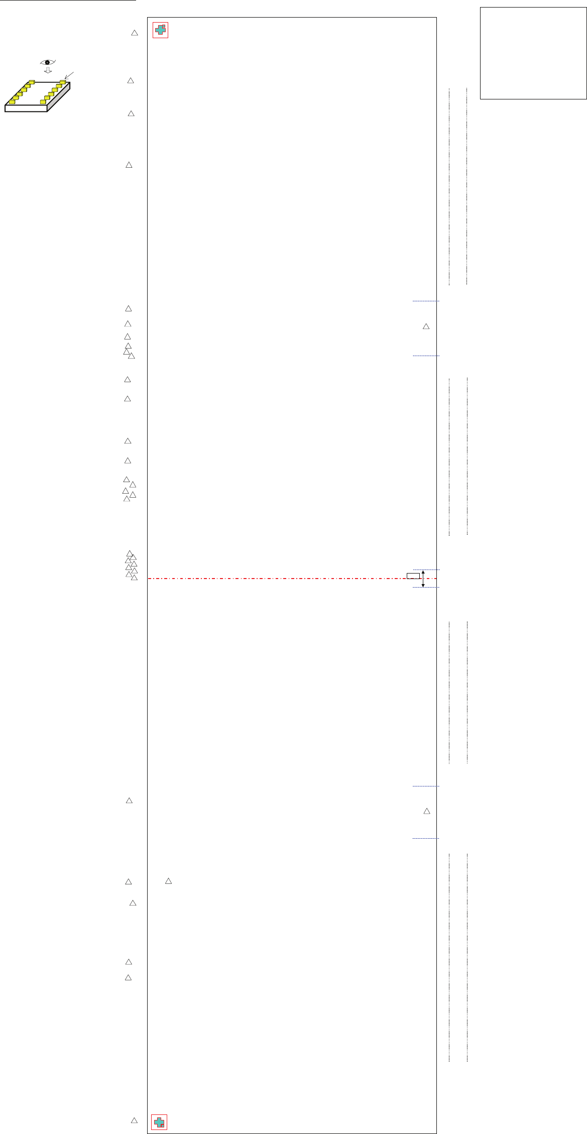
R61509V Pad Arrangement Rev 0.6
(1-a)
No
No □ DUMMYR4 1434
□DUMMYR3 1433
□TESTO15 1432
1DUMMYR1 □ □ VGLDMY4 1431
2DUMMYR2 □ □ G1 1430
3AGNDDUM1 □ □ G3 1429
4 VPP3B □ □ G5 1428
5 VPP3B □ □ G7 1427
6 VPP3B □ □ G9 1426
7 VPP3B □
8AGNDDUM2 □
9 VPP3A □
10 VPP3A □
11 VPP1 □
12 VPP1 □
13 VPP1 □
14 VPP1 □
15 VPP1 □
16 VPP1 □
17 VPP1 □
18 GNDDUM1 □
19 VDDTEST □ Connect to GNDDUM1
20 VREFC □ Connect to GNDDUM1
21 VREFD □ Open
22 VREF □ Open
23 VCCDUM1 □
24 DUMMYA □ Open
25 DUMMYA □ Open
26 DUMMYA □ Open
27 DUMMYA □ Open
28 DUMMYA □ Open
29 GNDDUM2 □
30 AGND □
31 AGND □
32 AGND □
33 AGND □
34 AGND □
35 AGND □
36 GND □
37 GND □
38 GND □
39 GND □
40 GND □
41 VCC □
42 VCC □
43 VCC □
44 VCC □
45 VCC □
46 VCC □
47 VCC □
48 TS8 □ Open
49 TS7 □ Open
50 TS6 □ Open
51 TS5 □ Open
52 TS4 □ Open
53 TS3 □ Open
54 TS2 □ Open
55 TS1 □ Open
56 TS0 □ Open
57 TEST5 □ Connect to GNDDUM3 □ G427 1217
58 TEST4 □ Connect to GNDDUM3 □ G429 1216
59 TEST3 □ Connect to GNDDUM3 □ G431 1215
60 TEST2 □ Connect to GNDDUM3 □VGLDMY3 1214
61 TEST1 □ Connect to GNDDUM3
62 GNDDUM3 □
63 TSC □ Connect to GNDDUM3
64 IM2 □ Connect to IOVCCDUM1/GNDDUM3
65 IM1 □ Connect to IOVCCDUM1/GNDDUM3
66 IM0_ID □Connect to IOVCCDUM1/GNDDUM3
67 IOVCCDUM1 □No PAD
68 PROTECT □
69 RESETX □
70 GNDDUM4 □
71 DUMMYB □ Open
72 DUMMYB □ Open
73 VSYNCX □
74 HSYNCX □ □ TESTO14 1213
75 IOVCCDUM2 □ □ S1 1212
76 ENABLE □ □ S2 1211
77 DOTCLK □ □ S3 1210
78 DB17 □ □ S4 1209
79 DB16 □ □ S5 1208
80 GNDDUM5 □
81 DB15 □
82 DB14 □
83 DB13 □
84 DB12 □
85 GNDDUM6 □
86 DB11 □
87 DB10 □
88 DB9 □
89 IOVCC □
90 IOVCC □
91 IOVCC □
92 IOVCC □
93 IOVCC □
94 IOVCC □
95 DB8 □
96 GNDDUM7 □
97 DB7 □
98 DB6 □
99 DB5 □
100 DB4 □
101 GNDDUM8 □
102 DB3 □
103 DB2 □
104 DB1 □
105 DB0 □
106 GNDDUM9 □
107 CSX □
108 RS □
109 WRX_SCL □
110 RDX □
111 GNDDUM10 □
112 FMARK □
113 SDI □
114 SDO □
115 VDD □
116 VDD □
117 VDD □
118 VDD □
119 VDD □
120 VDD □
121 VDD □ □ S356 857
122 VDD □ □ S357 856
123 VDD □ □ S358 855
124 VMON □ Open □ S359 854
125 VCOM □ □ S360 853
126 VCOM □ □ TESTO13 852
127 VCOM □ □ TESTO12 851
128 VCOM □ □ TESTO11 850
129 VCOM □ □ TESTO10 849
130 VCOM □
131 VCOM □
132 VCOM □
133 VCOMH □
134 VCOMH □ □ TESTO9 848
135 VCOMH □ □ TESTO8 847
136 VCOMH □ □ TESTO7 846
137 VCOMH □ □ TESTO6 845
138 VCOMH □ □ S361 844
139 VCOML □ □ S362 843
140 VCOML □ □ S363 842
141 VCOML □ □ S364 841
142 VCOML □ □ S365 840
143 VCOML □
144 VCOML □
145 GND □
146 GND □
147 GND □
148 GND □
149 GND □
150 GND □
151 GND □
152 GND □
153 GND □
154 VGS □
155 AGND □
156 AGND □
157 AGND □
158 AGND □
159 AGND □
160 AGND □
161 AGND □
162 AGND □
163 AGND □
164 VTEST □ Open
165 VCIR □ Open
166 VREG1OUT □
167 VCOMR □
168 C11M □
169 C11M □
170 C11M □
171 C11M □
172 C11M □
173 C11P □
174 C11P □
175 C11P □
176 C11P □
177 C11P □
178 C12M □
179 C12M □
180 C12M □ □ S716 489
181 C12M □ □ S717 488
182 C12M □ □ S718 487
183 C12P □ □ S719 486
184 C12P □ □ S720 485
185 C12P □ □ TESTO5 484
186 C12P □
187 C12P □
188 DDVDH □
189 DDVDH □
190 DDVDH □
191 DDVDH □
192 DDVDH □ No PAD
193 DDVDH □
194 DDVDH □
195 DDVDH □
196 DDVDH □
197 VCI1 □
198 VCI1 □
199 VCI1 □ □ VGLDMY2 483
200 VCI1 □ □ G432 482
201 VCI □ □ G430 481
202 VCI □ □ G428 480
203 VCI □
204 VCI □
205 VCI □
206 VCI □
207 VCILVL □
208 DUMMYC □ Open
209 DUMMYC □ Open
210 DUMMYC □ Open
211 DUMMYC □ Open
212 DUMMYC □ Open
213 GND □
214 GND □
215 GND □
216 GND □
217 GND □
218 AGND □
219 AGND □
220 AGND □
221 AGND □
222 AGND □
223 VGL □
224 VGL □
225 VGL □
226 VGL □
227 VGL □
228 VGL □
229 VGL □
230 VGL □
231 VGL □
232 AGNDDUM3 □
233 AGNDDUM4 □
234 VGH □
235 VGH □
236 VGH □
237 VGH □
238 VGH □
239 VGH □
240 AGNDDUM5 □
241 VCL □
242 VCL □
243 VCL □
244 C13M □
245 C13M □
246 C13M □
247 C13P □
248 C13P □
249 C13P □
250 C21M □
251 C21M □
252 C21M □
253 C21P □
254 C21P □
255 C21P □
256 C22M □
257 C22M □ □ G10 271
258 C22M □ □ G8 270
259 C22P □ □ G6 269
260 C22P □ □ G4 268
261 C22P □ □ G2 267
262 TESTO1 □ □ VGLDMY1 266
□TESTO4 265
□TESTO3 264
□TESTO2 263
(1-b)
Chip
BUMP
Top View
840um
Rev0.00 2007.12.13 First virsion
Rev0.10 2007.12.27 R61517's VCOMA, VCOMB --> R61509V's VCOM
Rev0.20 2008.02.13 Rev Mark 1 PAD No. 24~28, 71, 72, 208-217 changed to NC1-NC17
Rev0.21 2008.02.14 Rev Mark 2 NC's application voltage decided.
Rev0.30 2008.02.19 Rev Mark 4 VPP3C-->VPP3B, VPP2-->VPP1
Rev0.31 2008.02.27 Rev Mark 5 NC1-5-->DUMMYA
NC6-7-->DUMMYB
NC8-12-->DUMMYC
GNDDUM5-->GNDDUM2
GNDDUM6-->GNDDUM3
GNDDUM7-->GNDDUM4
GNDDUM8-->GNDDUM5
GNDDUM9-->GNDDUM6
GNDDUM10-->GNDDUM7
VLOUT1-->DDVDH
VLOUT2-->VGH
VLOUT3-->VGL
Rev0.4 2008.03.14 Rev Mark 6 DUMMYC's description "Open" added.
Rev0.5 2008.04.02 Rev Mark 7 Alignment mark (1-a) (1-b) added.
Rev0.6 2008.04.21 Rev Mark 8 Pin names changed.
Pad No66 IM0/ID→IM0_ID
Pad No69 RESET→RESETX
Pad No73 VSYNC→VSYNCX
Pad No74 HSYNC→HSYNCX
Pad No107 CS→CSX
Pad No109 WR/SCL→WRX_SCL
Pad No110 RD→RDX
1
1
1
1
1
1
1
1
1
1
3
4
4
5
5
5
5
5
5
5
5
5
5
5
5
5
7
7
6
8
8
8
8
8
8
8
R61509V Target Spec
Rev. 0.11 April 25, 2008, page 20 of 181
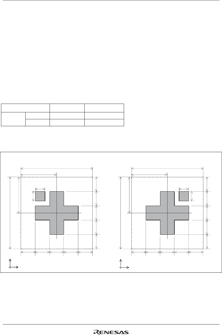
●Chip size: 19.03mm x 0.76mm
●Chip thickness: 280μm (typ)
●Pad coordinates: Pad center
●Coordinate origin: Chip center
●Au bump size
1. 50μm x 90μm (I/O side: No.1-262)
2. 15μm x 100μm (LCD output side: No.263-1434)
●Au bump pitch: See pad coordinate
●Au bump height:12μm
● Alignment mark
Table 10
Alignment marks X-axis Y-axis
(1-a) -9381.0 -251.0
Type A (1-b) 9381.0 -251.0
㩷
㩷
㩷
㩷
㩷X
Y
30um
30um
30um
30um
30um
20um
20um
30um 30um 30um 30um 30um
75um
75um
1-a: ( Left Alignment Mark )
150um : Alignment Mark Area X-size
150um : Alignment Mark Area
Y
-size
Alignment
Mark Area 30um
30um
30um
30um
30um
20um
20um
150um : Alignment Mark Area X-size
150um : Alignment Mark Area
Y
-size
30um 30um 30um 30um 30um
75um
75um
1-b: ( Right Alignment Mark )
Alignment
Mark Area
X
Y
Figure 2
R61509V Pad Coordinate (Unit:μm)2008.04.21 rev0.1
pad No pad name X Y pad No pad name X Y
1 DUMMYR1 -9135.0 -269.0 51 TS5 -5635.0 -269.0
2 DUMMYR2 -9065.0 -269.0 52 TS4 -5565.0 -269.0
3 AGNDDUM1 -8995.0 -269.0 53 TS3 -5495.0 -269.0
4 VPP3B -8925.0 -269.0 54 TS2 -5425.0 -269.0
5 VPP3B -8855.0 -269.0 55 TS1 -5355.0 -269.0
6 VPP3B -8785.0 -269.0 56 TS0 -5285.0 -269.0
7 VPP3B -8715.0 -269.0 57 TEST5 -5215.0 -269.0
8 AGNDDUM2 -8645.0 -269.0 58 TEST4 -5145.0 -269.0
9 VPP3A -8575.0 -269.0 59 TEST3 -5075.0 -269.0
10 VPP3A -8505.0 -269.0 60 TEST2 -5005.0 -269.0
11 VPP1 -8435.0 -269.0 61 TEST1 -4935.0 -269.0
12 VPP1 -8365.0 -269.0 62 GNDDUM3 -4865.0 -269.0
13 VPP1 -8295.0 -269.0 63 TSC -4795.0 -269.0
14 VPP1 -8225.0 -269.0 64 IM2 -4725.0 -269.0
15 VPP1 -8155.0 -269.0 65 IM1 -4655.0 -269.0
16 VPP1 -8085.0 -269.0 66 IM0_ID -4585.0 -269.0
17 VPP1 -8015.0 -269.0 67 IOVCCDUM1 -4515.0 -269.0
18 GNDDUM1 -7945.0 -269.0 68 PROTECT -4445.0 -269.0
19 VDDTEST -7875.0 -269.0 69 RESETX -4375.0 -269.0
20 VREFC -7805.0 -269.0 70 GNDDUM4 -4305.0 -269.0
21 VREFD -7735.0 -269.0 71 DUMMYB -4235.0 -269.0
22 VREF -7665.0 -269.0 72 DUMMYB -4165.0 -269.0
23 VCCDUM1 -7595.0 -269.0 73 VSYNCX -4095.0 -269.0
24 DUMMYA -7525.0 -269.0 74 HSYNCX -4025.0 -269.0
25 DUMMYA -7455.0 -269.0 75 IOVCCDUM2 -3955.0 -269.0
26 DUMMYA -7385.0 -269.0 76 ENABLE -3885.0 -269.0
27 DUMMYA -7315.0 -269.0 77 DOTCLK -3815.0 -269.0
28 DUMMYA -7245.0 -269.0 78 DB17 -3745.0 -269.0
29 GNDDUM2 -7175.0 -269.0 79 DB16 -3675.0 -269.0
30 AGND -7105.0 -269.0 80 GNDDUM5 -3605.0 -269.0
31 AGND -7035.0 -269.0 81 DB15 -3535.0 -269.0
32 AGND -6965.0 -269.0 82 DB14 -3465.0 -269.0
33 AGND -6895.0 -269.0 83 DB13 -3395.0 -269.0
34 AGND -6825.0 -269.0 84 DB12 -3325.0 -269.0
35 AGND -6755.0 -269.0 85 GNDDUM6 -3255.0 -269.0
36 GND -6685.0 -269.0 86 DB11 -3185.0 -269.0
37 GND -6615.0 -269.0 87 DB10 -3115.0 -269.0
38 GND -6545.0 -269.0 88 DB9 -3045.0 -269.0
39 GND -6475.0 -269.0 89 IOVCC -2975.0 -269.0
40 GND -6405.0 -269.0 90 IOVCC -2905.0 -269.0
41 VCC -6335.0 -269.0 91 IOVCC -2835.0 -269.0
42 VCC -6265.0 -269.0 92 IOVCC -2765.0 -269.0
43 VCC -6195.0 -269.0 93 IOVCC -2695.0 -269.0
44 VCC -6125.0 -269.0 94 IOVCC -2625.0 -269.0
45 VCC -6055.0 -269.0 95 DB8 -2555.0 -269.0
46 VCC -5985.0 -269.0 96 GNDDUM7 -2485.0 -269.0
47 VCC -5915.0 -269.0 97 DB7 -2415.0 -269.0
48 TS8 -5845.0 -269.0 98 DB6 -2345.0 -269.0
49 TS7 -5775.0 -269.0 99 DB5 -2275.0 -269.0
50 TS6 -5705.0 -269.0 100 DB4 -2205.0 -269.0

R61509V Pad Coordinate (Unit:μm)2008.04.21 rev0.1
pad No pad name X Y pad No pad name X Y
101 GNDDUM8 -2135.0 -269.0 151 GND 1365.0 -269.0
102 DB3 -2065.0 -269.0 152 GND 1435.0 -269.0
103 DB2 -1995.0 -269.0 153 GND 1505.0 -269.0
104 DB1 -1925.0 -269.0 154 VGS 1575.0 -269.0
105 DB0 -1855.0 -269.0 155 AGND 1645.0 -269.0
106 GNDDUM9 -1785.0 -269.0 156 AGND 1715.0 -269.0
107 CSX -1715.0 -269.0 157 AGND 1785.0 -269.0
108 RS -1645.0 -269.0 158 AGND 1855.0 -269.0
109 WRX_SCL -1575.0 -269.0 159 AGND 1925.0 -269.0
110 RDX -1505.0 -269.0 160 AGND 1995.0 -269.0
111 GNDDUM10 -1435.0 -269.0 161 AGND 2065.0 -269.0
112 FMARK -1365.0 -269.0 162 AGND 2135.0 -269.0
113 SDI -1295.0 -269.0 163 AGND 2205.0 -269.0
114 SDO -1225.0 -269.0 164 VTEST 2275.0 -269.0
115 VDD -1155.0 -269.0 165 VCIR 2345.0 -269.0
116 VDD -1085.0 -269.0 166 VREG1OUT 2415.0 -269.0
117 VDD -1015.0 -269.0 167 VCOMR 2485.0 -269.0
118 VDD -945.0 -269.0 168 C11M 2555.0 -269.0
119 VDD -875.0 -269.0 169 C11M 2625.0 -269.0
120 VDD -805.0 -269.0 170 C11M 2695.0 -269.0
121 VDD -735.0 -269.0 171 C11M 2765.0 -269.0
122 VDD -665.0 -269.0 172 C11M 2835.0 -269.0
123 VDD -595.0 -269.0 173 C11P 2905.0 -269.0
124 VMON -525.0 -269.0 174 C11P 2975.0 -269.0
125 VCOM -455.0 -269.0 175 C11P 3045.0 -269.0
126 VCOM -385.0 -269.0 176 C11P 3115.0 -269.0
127 VCOM -315.0 -269.0 177 C11P 3185.0 -269.0
128 VCOM -245.0 -269.0 178 C12M 3255.0 -269.0
129 VCOM -175.0 -269.0 179 C12M 3325.0 -269.0
130 VCOM -105.0 -269.0 180 C12M 3395.0 -269.0
131 VCOM -35.0 -269.0 181 C12M 3465.0 -269.0
132 VCOM 35.0 -269.0 182 C12M 3535.0 -269.0
133 VCOMH 105.0 -269.0 183 C12P 3605.0 -269.0
134 VCOMH 175.0 -269.0 184 C12P 3675.0 -269.0
135 VCOMH 245.0 -269.0 185 C12P 3745.0 -269.0
136 VCOMH 315.0 -269.0 186 C12P 3815.0 -269.0
137 VCOMH 385.0 -269.0 187 C12P 3885.0 -269.0
138 VCOMH 455.0 -269.0 188 DDVDH 3955.0 -269.0
139 VCOML 525.0 -269.0 189 DDVDH 4025.0 -269.0
140 VCOML 595.0 -269.0 190 DDVDH 4095.0 -269.0
141 VCOML 665.0 -269.0 191 DDVDH 4165.0 -269.0
142 VCOML 735.0 -269.0 192 DDVDH 4235.0 -269.0
143 VCOML 805.0 -269.0 193 DDVDH 4305.0 -269.0
144 VCOML 875.0 -269.0 194 DDVDH 4375.0 -269.0
145 GND 945.0 -269.0 195 DDVDH 4445.0 -269.0
146 GND 1015.0 -269.0 196 DDVDH 4515.0 -269.0
147 GND 1085.0 -269.0 197 VCI1 4585.0 -269.0
148 GND 1155.0 -269.0 198 VCI1 4655.0 -269.0
149 GND 1225.0 -269.0 199 VCI1 4725.0 -269.0
150 GND 1295.0 -269.0 200 VCI1 4795.0 -269.0

R61509V Pad Coordinate (Unit:μm)2008.04.21 rev0.1
pad No pad name X Y pad No pad name X Y
201 VCI 4865.0 -269.0 251 C21M 8365.0 -269.0
202 VCI 4935.0 -269.0 252 C21M 8435.0 -269.0
203 VCI 5005.0 -269.0 253 C21P 8505.0 -269.0
204 VCI 5075.0 -269.0 254 C21P 8575.0 -269.0
205 VCI 5145.0 -269.0 255 C21P 8645.0 -269.0
206 VCI 5215.0 -269.0 256 C22M 8715.0 -269.0
207 VCILVL 5285.0 -269.0 257 C22M 8785.0 -269.0
208 DUMMYC 5355.0 -269.0 258 C22M 8855.0 -269.0
209 DUMMYC 5425.0 -269.0 259 C22P 8925.0 -269.0
210 DUMMYC 5495.0 -269.0 260 C22P 8995.0 -269.0
211 DUMMYC 5565.0 -269.0 261 C22P 9065.0 -269.0
212 DUMMYC 5635.0 -269.0 262 TESTO1 9135.0 -269.0
213 GND 5705.0 -269.0 263 TESTO2 9397.5 157.0
214 GND 5775.0 -269.0 264 TESTO3 9382.5 276.0
215 GND 5845.0 -269.0 265 TESTO4 9367.5 157.0
216 GND 5915.0 -269.0 266 VGLDMY1 9352.5 276.0
217 GND 5985.0 -269.0 267 G2 9337.5 157.0
218 AGND 6055.0 -269.0 268 G4 9322.5 276.0
219 AGND 6125.0 -269.0 269 G6 9307.5 157.0
220 AGND 6195.0 -269.0 270 G8 9292.5 276.0
221 AGND 6265.0 -269.0 271 G10 9277.5 157.0
222 AGND 6335.0 -269.0 272 G12 9262.5 276.0
223 VGL 6405.0 -269.0 273 G14 9247.5 157.0
224 VGL 6475.0 -269.0 274 G16 9232.5 276.0
225 VGL 6545.0 -269.0 275 G18 9217.5 157.0
226 VGL 6615.0 -269.0 276 G20 9202.5 276.0
227 VGL 6685.0 -269.0 277 G22 9187.5 157.0
228 VGL 6755.0 -269.0 278 G24 9172.5 276.0
229 VGL 6825.0 -269.0 279 G26 9157.5 157.0
230 VGL 6895.0 -269.0 280 G28 9142.5 276.0
231 VGL 6965.0 -269.0 281 G30 9127.5 157.0
232 AGNDDUM3 7035.0 -269.0 282 G32 9112.5 276.0
233 AGNDDUM4 7105.0 -269.0 283 G34 9097.5 157.0
234 VGH 7175.0 -269.0 284 G36 9082.5 276.0
235 VGH 7245.0 -269.0 285 G38 9067.5 157.0
236 VGH 7315.0 -269.0 286 G40 9052.5 276.0
237 VGH 7385.0 -269.0 287 G42 9037.5 157.0
238 VGH 7455.0 -269.0 288 G44 9022.5 276.0
239 VGH 7525.0 -269.0 289 G46 9007.5 157.0
240 AGNDDUM5 7595.0 -269.0 290 G48 8992.5 276.0
241 VCL 7665.0 -269.0 291 G50 8977.5 157.0
242 VCL 7735.0 -269.0 292 G52 8962.5 276.0
243 VCL 7805.0 -269.0 293 G54 8947.5 157.0
244 C13M 7875.0 -269.0 294 G56 8932.5 276.0
245 C13M 7945.0 -269.0 295 G58 8917.5 157.0
246 C13M 8015.0 -269.0 296 G60 8902.5 276.0
247 C13P 8085.0 -269.0 297 G62 8887.5 157.0
248 C13P 8155.0 -269.0 298 G64 8872.5 276.0
249 C13P 8225.0 -269.0 299 G66 8857.5 157.0
250 C21M 8295.0 -269.0 300 G68 8842.5 276.0
R61509V Pad Coordinate (Unit:μm)2008.04.21 rev0.1
pad No pad name X Y pad No pad name X Y
301 G70 8827.5 157.0 351 G170 8077.5 157.0
302 G72 8812.5 276.0 352 G172 8062.5 276.0
303 G74 8797.5 157.0 353 G174 8047.5 157.0
304 G76 8782.5 276.0 354 G176 8032.5 276.0
305 G78 8767.5 157.0 355 G178 8017.5 157.0
306 G80 8752.5 276.0 356 G180 8002.5 276.0
307 G82 8737.5 157.0 357 G182 7987.5 157.0
308 G84 8722.5 276.0 358 G184 7972.5 276.0
309 G86 8707.5 157.0 359 G186 7957.5 157.0
310 G88 8692.5 276.0 360 G188 7942.5 276.0
311 G90 8677.5 157.0 361 G190 7927.5 157.0
312 G92 8662.5 276.0 362 G192 7912.5 276.0
313 G94 8647.5 157.0 363 G194 7897.5 157.0
314 G96 8632.5 276.0 364 G196 7882.5 276.0
315 G98 8617.5 157.0 365 G198 7867.5 157.0
316 G100 8602.5 276.0 366 G200 7852.5 276.0
317 G102 8587.5 157.0 367 G202 7837.5 157.0
318 G104 8572.5 276.0 368 G204 7822.5 276.0
319 G106 8557.5 157.0 369 G206 7807.5 157.0
320 G108 8542.5 276.0 370 G208 7792.5 276.0
321 G110 8527.5 157.0 371 G210 7777.5 157.0
322 G112 8512.5 276.0 372 G212 7762.5 276.0
323 G114 8497.5 157.0 373 G214 7747.5 157.0
324 G116 8482.5 276.0 374 G216 7732.5 276.0
325 G118 8467.5 157.0 375 G218 7717.5 157.0
326 G120 8452.5 276.0 376 G220 7702.5 276.0
327 G122 8437.5 157.0 377 G222 7687.5 157.0
328 G124 8422.5 276.0 378 G224 7672.5 276.0
329 G126 8407.5 157.0 379 G226 7657.5 157.0
330 G128 8392.5 276.0 380 G228 7642.5 276.0
331 G130 8377.5 157.0 381 G230 7627.5 157.0
332 G132 8362.5 276.0 382 G232 7612.5 276.0
333 G134 8347.5 157.0 383 G234 7597.5 157.0
334 G136 8332.5 276.0 384 G236 7582.5 276.0
335 G138 8317.5 157.0 385 G238 7567.5 157.0
336 G140 8302.5 276.0 386 G240 7552.5 276.0
337 G142 8287.5 157.0 387 G242 7537.5 157.0
338 G144 8272.5 276.0 388 G244 7522.5 276.0
339 G146 8257.5 157.0 389 G246 7507.5 157.0
340 G148 8242.5 276.0 390 G248 7492.5 276.0
341 G150 8227.5 157.0 391 G250 7477.5 157.0
342 G152 8212.5 276.0 392 G252 7462.5 276.0
343 G154 8197.5 157.0 393 G254 7447.5 157.0
344 G156 8182.5 276.0 394 G256 7432.5 276.0
345 G158 8167.5 157.0 395 G258 7417.5 157.0
346 G160 8152.5 276.0 396 G260 7402.5 276.0
347 G162 8137.5 157.0 397 G262 7387.5 157.0
348 G164 8122.5 276.0 398 G264 7372.5 276.0
349 G166 8107.5 157.0 399 G266 7357.5 157.0
350 G168 8092.5 276.0 400 G268 7342.5 276.0

R61509V Pad Coordinate (Unit:μm)2008.04.21 rev0.1
pad No pad name X Y pad No pad name X Y
401 G270 7327.5 157.0 451 G370 6577.5 157.0
402 G272 7312.5 276.0 452 G372 6562.5 276.0
403 G274 7297.5 157.0 453 G374 6547.5 157.0
404 G276 7282.5 276.0 454 G376 6532.5 276.0
405 G278 7267.5 157.0 455 G378 6517.5 157.0
406 G280 7252.5 276.0 456 G380 6502.5 276.0
407 G282 7237.5 157.0 457 G382 6487.5 157.0
408 G284 7222.5 276.0 458 G384 6472.5 276.0
409 G286 7207.5 157.0 459 G386 6457.5 157.0
410 G288 7192.5 276.0 460 G388 6442.5 276.0
411 G290 7177.5 157.0 461 G390 6427.5 157.0
412 G292 7162.5 276.0 462 G392 6412.5 276.0
413 G294 7147.5 157.0 463 G394 6397.5 157.0
414 G296 7132.5 276.0 464 G396 6382.5 276.0
415 G298 7117.5 157.0 465 G398 6367.5 157.0
416 G300 7102.5 276.0 466 G400 6352.5 276.0
417 G302 7087.5 157.0 467 G402 6337.5 157.0
418 G304 7072.5 276.0 468 G404 6322.5 276.0
419 G306 7057.5 157.0 469 G406 6307.5 157.0
420 G308 7042.5 276.0 470 G408 6292.5 276.0
421 G310 7027.5 157.0 471 G410 6277.5 157.0
422 G312 7012.5 276.0 472 G412 6262.5 276.0
423 G314 6997.5 157.0 473 G414 6247.5 157.0
424 G316 6982.5 276.0 474 G416 6232.5 276.0
425 G318 6967.5 157.0 475 G418 6217.5 157.0
426 G320 6952.5 276.0 476 G420 6202.5 276.0
427 G322 6937.5 157.0 477 G422 6187.5 157.0
428 G324 6922.5 276.0 478 G424 6172.5 276.0
429 G326 6907.5 157.0 479 G426 6157.5 157.0
430 G328 6892.5 276.0 480 G428 6142.5 276.0
431 G330 6877.5 157.0 481 G430 6127.5 157.0
432 G332 6862.5 276.0 482 G432 6112.5 276.0
433 G334 6847.5 157.0 483 VGLDMY2 6097.5 157.0
434 G336 6832.5 276.0 484 TESTO5 5887.5 157.0
435 G338 6817.5 157.0 485 S720 5872.5 276.0
436 G340 6802.5 276.0 486 S719 5857.5 157.0
437 G342 6787.5 157.0 487 S718 5842.5 276.0
438 G344 6772.5 276.0 488 S717 5827.5 157.0
439 G346 6757.5 157.0 489 S716 5812.5 276.0
440 G348 6742.5 276.0 490 S715 5797.5 157.0
441 G350 6727.5 157.0 491 S714 5782.5 276.0
442 G352 6712.5 276.0 492 S713 5767.5 157.0
443 G354 6697.5 157.0 493 S712 5752.5 276.0
444 G356 6682.5 276.0 494 S711 5737.5 157.0
445 G358 6667.5 157.0 495 S710 5722.5 276.0
446 G360 6652.5 276.0 496 S709 5707.5 157.0
447 G362 6637.5 157.0 497 S708 5692.5 276.0
448 G364 6622.5 276.0 498 S707 5677.5 157.0
449 G366 6607.5 157.0 499 S706 5662.5 276.0
450 G368 6592.5 276.0 500 S705 5647.5 157.0

R61509V Pad Coordinate (Unit:μm)2008.04.21 rev0.1
pad No pad name X Y pad No pad name X Y
501 S704 5632.5 276.0 551 S654 4882.5 276.0
502 S703 5617.5 157.0 552 S653 4867.5 157.0
503 S702 5602.5 276.0 553 S652 4852.5 276.0
504 S701 5587.5 157.0 554 S651 4837.5 157.0
505 S700 5572.5 276.0 555 S650 4822.5 276.0
506 S699 5557.5 157.0 556 S649 4807.5 157.0
507 S698 5542.5 276.0 557 S648 4792.5 276.0
508 S697 5527.5 157.0 558 S647 4777.5 157.0
509 S696 5512.5 276.0 559 S646 4762.5 276.0
510 S695 5497.5 157.0 560 S645 4747.5 157.0
511 S694 5482.5 276.0 561 S644 4732.5 276.0
512 S693 5467.5 157.0 562 S643 4717.5 157.0
513 S692 5452.5 276.0 563 S642 4702.5 276.0
514 S691 5437.5 157.0 564 S641 4687.5 157.0
515 S690 5422.5 276.0 565 S640 4672.5 276.0
516 S689 5407.5 157.0 566 S639 4657.5 157.0
517 S688 5392.5 276.0 567 S638 4642.5 276.0
518 S687 5377.5 157.0 568 S637 4627.5 157.0
519 S686 5362.5 276.0 569 S636 4612.5 276.0
520 S685 5347.5 157.0 570 S635 4597.5 157.0
521 S684 5332.5 276.0 571 S634 4582.5 276.0
522 S683 5317.5 157.0 572 S633 4567.5 157.0
523 S682 5302.5 276.0 573 S632 4552.5 276.0
524 S681 5287.5 157.0 574 S631 4537.5 157.0
525 S680 5272.5 276.0 575 S630 4522.5 276.0
526 S679 5257.5 157.0 576 S629 4507.5 157.0
527 S678 5242.5 276.0 577 S628 4492.5 276.0
528 S677 5227.5 157.0 578 S627 4477.5 157.0
529 S676 5212.5 276.0 579 S626 4462.5 276.0
530 S675 5197.5 157.0 580 S625 4447.5 157.0
531 S674 5182.5 276.0 581 S624 4432.5 276.0
532 S673 5167.5 157.0 582 S623 4417.5 157.0
533 S672 5152.5 276.0 583 S622 4402.5 276.0
534 S671 5137.5 157.0 584 S621 4387.5 157.0
535 S670 5122.5 276.0 585 S620 4372.5 276.0
536 S669 5107.5 157.0 586 S619 4357.5 157.0
537 S668 5092.5 276.0 587 S618 4342.5 276.0
538 S667 5077.5 157.0 588 S617 4327.5 157.0
539 S666 5062.5 276.0 589 S616 4312.5 276.0
540 S665 5047.5 157.0 590 S615 4297.5 157.0
541 S664 5032.5 276.0 591 S614 4282.5 276.0
542 S663 5017.5 157.0 592 S613 4267.5 157.0
543 S662 5002.5 276.0 593 S612 4252.5 276.0
544 S661 4987.5 157.0 594 S611 4237.5 157.0
545 S660 4972.5 276.0 595 S610 4222.5 276.0
546 S659 4957.5 157.0 596 S609 4207.5 157.0
547 S658 4942.5 276.0 597 S608 4192.5 276.0
548 S657 4927.5 157.0 598 S607 4177.5 157.0
549 S656 4912.5 276.0 599 S606 4162.5 276.0
550 S655 4897.5 157.0 600 S605 4147.5 157.0

R61509V Pad Coordinate (Unit:μm)2008.04.21 rev0.1
pad No pad name X Y pad No pad name X Y
601 S604 4132.5 276.0 651 S554 3382.5 276.0
602 S603 4117.5 157.0 652 S553 3367.5 157.0
603 S602 4102.5 276.0 653 S552 3352.5 276.0
604 S601 4087.5 157.0 654 S551 3337.5 157.0
605 S600 4072.5 276.0 655 S550 3322.5 276.0
606 S599 4057.5 157.0 656 S549 3307.5 157.0
607 S598 4042.5 276.0 657 S548 3292.5 276.0
608 S597 4027.5 157.0 658 S547 3277.5 157.0
609 S596 4012.5 276.0 659 S546 3262.5 276.0
610 S595 3997.5 157.0 660 S545 3247.5 157.0
611 S594 3982.5 276.0 661 S544 3232.5 276.0
612 S593 3967.5 157.0 662 S543 3217.5 157.0
613 S592 3952.5 276.0 663 S542 3202.5 276.0
614 S591 3937.5 157.0 664 S541 3187.5 157.0
615 S590 3922.5 276.0 665 S540 3172.5 276.0
616 S589 3907.5 157.0 666 S539 3157.5 157.0
617 S588 3892.5 276.0 667 S538 3142.5 276.0
618 S587 3877.5 157.0 668 S537 3127.5 157.0
619 S586 3862.5 276.0 669 S536 3112.5 276.0
620 S585 3847.5 157.0 670 S535 3097.5 157.0
621 S584 3832.5 276.0 671 S534 3082.5 276.0
622 S583 3817.5 157.0 672 S533 3067.5 157.0
623 S582 3802.5 276.0 673 S532 3052.5 276.0
624 S581 3787.5 157.0 674 S531 3037.5 157.0
625 S580 3772.5 276.0 675 S530 3022.5 276.0
626 S579 3757.5 157.0 676 S529 3007.5 157.0
627 S578 3742.5 276.0 677 S528 2992.5 276.0
628 S577 3727.5 157.0 678 S527 2977.5 157.0
629 S576 3712.5 276.0 679 S526 2962.5 276.0
630 S575 3697.5 157.0 680 S525 2947.5 157.0
631 S574 3682.5 276.0 681 S524 2932.5 276.0
632 S573 3667.5 157.0 682 S523 2917.5 157.0
633 S572 3652.5 276.0 683 S522 2902.5 276.0
634 S571 3637.5 157.0 684 S521 2887.5 157.0
635 S570 3622.5 276.0 685 S520 2872.5 276.0
636 S569 3607.5 157.0 686 S519 2857.5 157.0
637 S568 3592.5 276.0 687 S518 2842.5 276.0
638 S567 3577.5 157.0 688 S517 2827.5 157.0
639 S566 3562.5 276.0 689 S516 2812.5 276.0
640 S565 3547.5 157.0 690 S515 2797.5 157.0
641 S564 3532.5 276.0 691 S514 2782.5 276.0
642 S563 3517.5 157.0 692 S513 2767.5 157.0
643 S562 3502.5 276.0 693 S512 2752.5 276.0
644 S561 3487.5 157.0 694 S511 2737.5 157.0
645 S560 3472.5 276.0 695 S510 2722.5 276.0
646 S559 3457.5 157.0 696 S509 2707.5 157.0
647 S558 3442.5 276.0 697 S508 2692.5 276.0
648 S557 3427.5 157.0 698 S507 2677.5 157.0
649 S556 3412.5 276.0 699 S506 2662.5 276.0
650 S555 3397.5 157.0 700 S505 2647.5 157.0

R61509V Pad Coordinate (Unit:μm)2008.04.21 rev0.1
pad No pad name X Y pad No pad name X Y
701 S504 2632.5 276.0 751 S454 1882.5 276.0
702 S503 2617.5 157.0 752 S453 1867.5 157.0
703 S502 2602.5 276.0 753 S452 1852.5 276.0
704 S501 2587.5 157.0 754 S451 1837.5 157.0
705 S500 2572.5 276.0 755 S450 1822.5 276.0
706 S499 2557.5 157.0 756 S449 1807.5 157.0
707 S498 2542.5 276.0 757 S448 1792.5 276.0
708 S497 2527.5 157.0 758 S447 1777.5 157.0
709 S496 2512.5 276.0 759 S446 1762.5 276.0
710 S495 2497.5 157.0 760 S445 1747.5 157.0
711 S494 2482.5 276.0 761 S444 1732.5 276.0
712 S493 2467.5 157.0 762 S443 1717.5 157.0
713 S492 2452.5 276.0 763 S442 1702.5 276.0
714 S491 2437.5 157.0 764 S441 1687.5 157.0
715 S490 2422.5 276.0 765 S440 1672.5 276.0
716 S489 2407.5 157.0 766 S439 1657.5 157.0
717 S488 2392.5 276.0 767 S438 1642.5 276.0
718 S487 2377.5 157.0 768 S437 1627.5 157.0
719 S486 2362.5 276.0 769 S436 1612.5 276.0
720 S485 2347.5 157.0 770 S435 1597.5 157.0
721 S484 2332.5 276.0 771 S434 1582.5 276.0
722 S483 2317.5 157.0 772 S433 1567.5 157.0
723 S482 2302.5 276.0 773 S432 1552.5 276.0
724 S481 2287.5 157.0 774 S431 1537.5 157.0
725 S480 2272.5 276.0 775 S430 1522.5 276.0
726 S479 2257.5 157.0 776 S429 1507.5 157.0
727 S478 2242.5 276.0 777 S428 1492.5 276.0
728 S477 2227.5 157.0 778 S427 1477.5 157.0
729 S476 2212.5 276.0 779 S426 1462.5 276.0
730 S475 2197.5 157.0 780 S425 1447.5 157.0
731 S474 2182.5 276.0 781 S424 1432.5 276.0
732 S473 2167.5 157.0 782 S423 1417.5 157.0
733 S472 2152.5 276.0 783 S422 1402.5 276.0
734 S471 2137.5 157.0 784 S421 1387.5 157.0
735 S470 2122.5 276.0 785 S420 1372.5 276.0
736 S469 2107.5 157.0 786 S419 1357.5 157.0
737 S468 2092.5 276.0 787 S418 1342.5 276.0
738 S467 2077.5 157.0 788 S417 1327.5 157.0
739 S466 2062.5 276.0 789 S416 1312.5 276.0
740 S465 2047.5 157.0 790 S415 1297.5 157.0
741 S464 2032.5 276.0 791 S414 1282.5 276.0
742 S463 2017.5 157.0 792 S413 1267.5 157.0
743 S462 2002.5 276.0 793 S412 1252.5 276.0
744 S461 1987.5 157.0 794 S411 1237.5 157.0
745 S460 1972.5 276.0 795 S410 1222.5 276.0
746 S459 1957.5 157.0 796 S409 1207.5 157.0
747 S458 1942.5 276.0 797 S408 1192.5 276.0
748 S457 1927.5 157.0 798 S407 1177.5 157.0
749 S456 1912.5 276.0 799 S406 1162.5 276.0
750 S455 1897.5 157.0 800 S405 1147.5 157.0

R61509V Pad Coordinate (Unit:μm)2008.04.21 rev0.1
pad No pad name X Y pad No pad name X Y
801 S404 1132.5 276.0 851 TESTO12 -457.5 276.0
802 S403 1117.5 157.0 852 TESTO13 -472.5 157.0
803 S402 1102.5 276.0 853 S360 -487.5 276.0
804 S401 1087.5 157.0 854 S359 -502.5 157.0
805 S400 1072.5 276.0 855 S358 -517.5 276.0
806 S399 1057.5 157.0 856 S357 -532.5 157.0
807 S398 1042.5 276.0 857 S356 -547.5 276.0
808 S397 1027.5 157.0 858 S355 -562.5 157.0
809 S396 1012.5 276.0 859 S354 -577.5 276.0
810 S395 997.5 157.0 860 S353 -592.5 157.0
811 S394 982.5 276.0 861 S352 -607.5 276.0
812 S393 967.5 157.0 862 S351 -622.5 157.0
813 S392 952.5 276.0 863 S350 -637.5 276.0
814 S391 937.5 157.0 864 S349 -652.5 157.0
815 S390 922.5 276.0 865 S348 -667.5 276.0
816 S389 907.5 157.0 866 S347 -682.5 157.0
817 S388 892.5 276.0 867 S346 -697.5 276.0
818 S387 877.5 157.0 868 S345 -712.5 157.0
819 S386 862.5 276.0 869 S344 -727.5 276.0
820 S385 847.5 157.0 870 S343 -742.5 157.0
821 S384 832.5 276.0 871 S342 -757.5 276.0
822 S383 817.5 157.0 872 S341 -772.5 157.0
823 S382 802.5 276.0 873 S340 -787.5 276.0
824 S381 787.5 157.0 874 S339 -802.5 157.0
825 S380 772.5 276.0 875 S338 -817.5 276.0
826 S379 757.5 157.0 876 S337 -832.5 157.0
827 S378 742.5 276.0 877 S336 -847.5 276.0
828 S377 727.5 157.0 878 S335 -862.5 157.0
829 S376 712.5 276.0 879 S334 -877.5 276.0
830 S375 697.5 157.0 880 S333 -892.5 157.0
831 S374 682.5 276.0 881 S332 -907.5 276.0
832 S373 667.5 157.0 882 S331 -922.5 157.0
833 S372 652.5 276.0 883 S330 -937.5 276.0
834 S371 637.5 157.0 884 S329 -952.5 157.0
835 S370 622.5 276.0 885 S328 -967.5 276.0
836 S369 607.5 157.0 886 S327 -982.5 157.0
837 S368 592.5 276.0 887 S326 -997.5 276.0
838 S367 577.5 157.0 888 S325 -1012.5 157.0
839 S366 562.5 276.0 889 S324 -1027.5 276.0
840 S365 547.5 157.0 890 S323 -1042.5 157.0
841 S364 532.5 276.0 891 S322 -1057.5 276.0
842 S363 517.5 157.0 892 S321 -1072.5 157.0
843 S362 502.5 276.0 893 S320 -1087.5 276.0
844 S361 487.5 157.0 894 S319 -1102.5 157.0
845 TESTO6 472.5 276.0 895 S318 -1117.5 276.0
846 TESTO7 457.5 157.0 896 S317 -1132.5 157.0
847 TESTO8 442.5 276.0 897 S316 -1147.5 276.0
848 TESTO9 427.5 157.0 898 S315 -1162.5 157.0
849 TESTO10 -427.5 276.0 899 S314 -1177.5 276.0
850 TESTO11 -442.5 157.0 900 S313 -1192.5 157.0

R61509V Pad Coordinate (Unit:μm)2008.04.21 rev0.1
pad No pad name X Y pad No pad name X Y
901 S312 -1207.5 276.0 951 S262 -1957.5 276.0
902 S311 -1222.5 157.0 952 S261 -1972.5 157.0
903 S310 -1237.5 276.0 953 S260 -1987.5 276.0
904 S309 -1252.5 157.0 954 S259 -2002.5 157.0
905 S308 -1267.5 276.0 955 S258 -2017.5 276.0
906 S307 -1282.5 157.0 956 S257 -2032.5 157.0
907 S306 -1297.5 276.0 957 S256 -2047.5 276.0
908 S305 -1312.5 157.0 958 S255 -2062.5 157.0
909 S304 -1327.5 276.0 959 S254 -2077.5 276.0
910 S303 -1342.5 157.0 960 S253 -2092.5 157.0
911 S302 -1357.5 276.0 961 S252 -2107.5 276.0
912 S301 -1372.5 157.0 962 S251 -2122.5 157.0
913 S300 -1387.5 276.0 963 S250 -2137.5 276.0
914 S299 -1402.5 157.0 964 S249 -2152.5 157.0
915 S298 -1417.5 276.0 965 S248 -2167.5 276.0
916 S297 -1432.5 157.0 966 S247 -2182.5 157.0
917 S296 -1447.5 276.0 967 S246 -2197.5 276.0
918 S295 -1462.5 157.0 968 S245 -2212.5 157.0
919 S294 -1477.5 276.0 969 S244 -2227.5 276.0
920 S293 -1492.5 157.0 970 S243 -2242.5 157.0
921 S292 -1507.5 276.0 971 S242 -2257.5 276.0
922 S291 -1522.5 157.0 972 S241 -2272.5 157.0
923 S290 -1537.5 276.0 973 S240 -2287.5 276.0
924 S289 -1552.5 157.0 974 S239 -2302.5 157.0
925 S288 -1567.5 276.0 975 S238 -2317.5 276.0
926 S287 -1582.5 157.0 976 S237 -2332.5 157.0
927 S286 -1597.5 276.0 977 S236 -2347.5 276.0
928 S285 -1612.5 157.0 978 S235 -2362.5 157.0
929 S284 -1627.5 276.0 979 S234 -2377.5 276.0
930 S283 -1642.5 157.0 980 S233 -2392.5 157.0
931 S282 -1657.5 276.0 981 S232 -2407.5 276.0
932 S281 -1672.5 157.0 982 S231 -2422.5 157.0
933 S280 -1687.5 276.0 983 S230 -2437.5 276.0
934 S279 -1702.5 157.0 984 S229 -2452.5 157.0
935 S278 -1717.5 276.0 985 S228 -2467.5 276.0
936 S277 -1732.5 157.0 986 S227 -2482.5 157.0
937 S276 -1747.5 276.0 987 S226 -2497.5 276.0
938 S275 -1762.5 157.0 988 S225 -2512.5 157.0
939 S274 -1777.5 276.0 989 S224 -2527.5 276.0
940 S273 -1792.5 157.0 990 S223 -2542.5 157.0
941 S272 -1807.5 276.0 991 S222 -2557.5 276.0
942 S271 -1822.5 157.0 992 S221 -2572.5 157.0
943 S270 -1837.5 276.0 993 S220 -2587.5 276.0
944 S269 -1852.5 157.0 994 S219 -2602.5 157.0
945 S268 -1867.5 276.0 995 S218 -2617.5 276.0
946 S267 -1882.5 157.0 996 S217 -2632.5 157.0
947 S266 -1897.5 276.0 997 S216 -2647.5 276.0
948 S265 -1912.5 157.0 998 S215 -2662.5 157.0
949 S264 -1927.5 276.0 999 S214 -2677.5 276.0
950 S263 -1942.5 157.0 1000 S213 -2692.5 157.0

R61509V Pad Coordinate (Unit:μm)2008.04.21 rev0.1
pad No pad name X Y pad No pad name X Y
1001 S212 -2707.5 276.0 1051 S162 -3457.5 276.0
1002 S211 -2722.5 157.0 1052 S161 -3472.5 157.0
1003 S210 -2737.5 276.0 1053 S160 -3487.5 276.0
1004 S209 -2752.5 157.0 1054 S159 -3502.5 157.0
1005 S208 -2767.5 276.0 1055 S158 -3517.5 276.0
1006 S207 -2782.5 157.0 1056 S157 -3532.5 157.0
1007 S206 -2797.5 276.0 1057 S156 -3547.5 276.0
1008 S205 -2812.5 157.0 1058 S155 -3562.5 157.0
1009 S204 -2827.5 276.0 1059 S154 -3577.5 276.0
1010 S203 -2842.5 157.0 1060 S153 -3592.5 157.0
1011 S202 -2857.5 276.0 1061 S152 -3607.5 276.0
1012 S201 -2872.5 157.0 1062 S151 -3622.5 157.0
1013 S200 -2887.5 276.0 1063 S150 -3637.5 276.0
1014 S199 -2902.5 157.0 1064 S149 -3652.5 157.0
1015 S198 -2917.5 276.0 1065 S148 -3667.5 276.0
1016 S197 -2932.5 157.0 1066 S147 -3682.5 157.0
1017 S196 -2947.5 276.0 1067 S146 -3697.5 276.0
1018 S195 -2962.5 157.0 1068 S145 -3712.5 157.0
1019 S194 -2977.5 276.0 1069 S144 -3727.5 276.0
1020 S193 -2992.5 157.0 1070 S143 -3742.5 157.0
1021 S192 -3007.5 276.0 1071 S142 -3757.5 276.0
1022 S191 -3022.5 157.0 1072 S141 -3772.5 157.0
1023 S190 -3037.5 276.0 1073 S140 -3787.5 276.0
1024 S189 -3052.5 157.0 1074 S139 -3802.5 157.0
1025 S188 -3067.5 276.0 1075 S138 -3817.5 276.0
1026 S187 -3082.5 157.0 1076 S137 -3832.5 157.0
1027 S186 -3097.5 276.0 1077 S136 -3847.5 276.0
1028 S185 -3112.5 157.0 1078 S135 -3862.5 157.0
1029 S184 -3127.5 276.0 1079 S134 -3877.5 276.0
1030 S183 -3142.5 157.0 1080 S133 -3892.5 157.0
1031 S182 -3157.5 276.0 1081 S132 -3907.5 276.0
1032 S181 -3172.5 157.0 1082 S131 -3922.5 157.0
1033 S180 -3187.5 276.0 1083 S130 -3937.5 276.0
1034 S179 -3202.5 157.0 1084 S129 -3952.5 157.0
1035 S178 -3217.5 276.0 1085 S128 -3967.5 276.0
1036 S177 -3232.5 157.0 1086 S127 -3982.5 157.0
1037 S176 -3247.5 276.0 1087 S126 -3997.5 276.0
1038 S175 -3262.5 157.0 1088 S125 -4012.5 157.0
1039 S174 -3277.5 276.0 1089 S124 -4027.5 276.0
1040 S173 -3292.5 157.0 1090 S123 -4042.5 157.0
1041 S172 -3307.5 276.0 1091 S122 -4057.5 276.0
1042 S171 -3322.5 157.0 1092 S121 -4072.5 157.0
1043 S170 -3337.5 276.0 1093 S120 -4087.5 276.0
1044 S169 -3352.5 157.0 1094 S119 -4102.5 157.0
1045 S168 -3367.5 276.0 1095 S118 -4117.5 276.0
1046 S167 -3382.5 157.0 1096 S117 -4132.5 157.0
1047 S166 -3397.5 276.0 1097 S116 -4147.5 276.0
1048 S165 -3412.5 157.0 1098 S115 -4162.5 157.0
1049 S164 -3427.5 276.0 1099 S114 -4177.5 276.0
1050 S163 -3442.5 157.0 1100 S113 -4192.5 157.0

R61509V Pad Coordinate (Unit:μm)2008.04.21 rev0.1
pad No pad name X Y pad No pad name X Y
1101 S112 -4207.5 276.0 1151 S62 -4957.5 276.0
1102 S111 -4222.5 157.0 1152 S61 -4972.5 157.0
1103 S110 -4237.5 276.0 1153 S60 -4987.5 276.0
1104 S109 -4252.5 157.0 1154 S59 -5002.5 157.0
1105 S108 -4267.5 276.0 1155 S58 -5017.5 276.0
1106 S107 -4282.5 157.0 1156 S57 -5032.5 157.0
1107 S106 -4297.5 276.0 1157 S56 -5047.5 276.0
1108 S105 -4312.5 157.0 1158 S55 -5062.5 157.0
1109 S104 -4327.5 276.0 1159 S54 -5077.5 276.0
1110 S103 -4342.5 157.0 1160 S53 -5092.5 157.0
1111 S102 -4357.5 276.0 1161 S52 -5107.5 276.0
1112 S101 -4372.5 157.0 1162 S51 -5122.5 157.0
1113 S100 -4387.5 276.0 1163 S50 -5137.5 276.0
1114 S99 -4402.5 157.0 1164 S49 -5152.5 157.0
1115 S98 -4417.5 276.0 1165 S48 -5167.5 276.0
1116 S97 -4432.5 157.0 1166 S47 -5182.5 157.0
1117 S96 -4447.5 276.0 1167 S46 -5197.5 276.0
1118 S95 -4462.5 157.0 1168 S45 -5212.5 157.0
1119 S94 -4477.5 276.0 1169 S44 -5227.5 276.0
1120 S93 -4492.5 157.0 1170 S43 -5242.5 157.0
1121 S92 -4507.5 276.0 1171 S42 -5257.5 276.0
1122 S91 -4522.5 157.0 1172 S41 -5272.5 157.0
1123 S90 -4537.5 276.0 1173 S40 -5287.5 276.0
1124 S89 -4552.5 157.0 1174 S39 -5302.5 157.0
1125 S88 -4567.5 276.0 1175 S38 -5317.5 276.0
1126 S87 -4582.5 157.0 1176 S37 -5332.5 157.0
1127 S86 -4597.5 276.0 1177 S36 -5347.5 276.0
1128 S85 -4612.5 157.0 1178 S35 -5362.5 157.0
1129 S84 -4627.5 276.0 1179 S34 -5377.5 276.0
1130 S83 -4642.5 157.0 1180 S33 -5392.5 157.0
1131 S82 -4657.5 276.0 1181 S32 -5407.5 276.0
1132 S81 -4672.5 157.0 1182 S31 -5422.5 157.0
1133 S80 -4687.5 276.0 1183 S30 -5437.5 276.0
1134 S79 -4702.5 157.0 1184 S29 -5452.5 157.0
1135 S78 -4717.5 276.0 1185 S28 -5467.5 276.0
1136 S77 -4732.5 157.0 1186 S27 -5482.5 157.0
1137 S76 -4747.5 276.0 1187 S26 -5497.5 276.0
1138 S75 -4762.5 157.0 1188 S25 -5512.5 157.0
1139 S74 -4777.5 276.0 1189 S24 -5527.5 276.0
1140 S73 -4792.5 157.0 1190 S23 -5542.5 157.0
1141 S72 -4807.5 276.0 1191 S22 -5557.5 276.0
1142 S71 -4822.5 157.0 1192 S21 -5572.5 157.0
1143 S70 -4837.5 276.0 1193 S20 -5587.5 276.0
1144 S69 -4852.5 157.0 1194 S19 -5602.5 157.0
1145 S68 -4867.5 276.0 1195 S18 -5617.5 276.0
1146 S67 -4882.5 157.0 1196 S17 -5632.5 157.0
1147 S66 -4897.5 276.0 1197 S16 -5647.5 276.0
1148 S65 -4912.5 157.0 1198 S15 -5662.5 157.0
1149 S64 -4927.5 276.0 1199 S14 -5677.5 276.0
1150 S63 -4942.5 157.0 1200 S13 -5692.5 157.0

R61509V Pad Coordinate (Unit:μm)2008.04.21 rev0.1
pad No pad name X Y pad No pad name X Y
1201 S12 -5707.5 276.0 1251 G359 -6652.5 157.0
1202 S11 -5722.5 157.0 1252 G357 -6667.5 276.0
1203 S10 -5737.5 276.0 1253 G355 -6682.5 157.0
1204 S9 -5752.5 157.0 1254 G353 -6697.5 276.0
1205 S8 -5767.5 276.0 1255 G351 -6712.5 157.0
1206 S7 -5782.5 157.0 1256 G349 -6727.5 276.0
1207 S6 -5797.5 276.0 1257 G347 -6742.5 157.0
1208 S5 -5812.5 157.0 1258 G345 -6757.5 276.0
1209 S4 -5827.5 276.0 1259 G343 -6772.5 157.0
1210 S3 -5842.5 157.0 1260 G341 -6787.5 276.0
1211 S2 -5857.5 276.0 1261 G339 -6802.5 157.0
1212 S1 -5872.5 157.0 1262 G337 -6817.5 276.0
1213 TESTO14 -5887.5 276.0 1263 G335 -6832.5 157.0
1214 VGLDMY3 -6097.5 276.0 1264 G333 -6847.5 276.0
1215 G431 -6112.5 157.0 1265 G331 -6862.5 157.0
1216 G429 -6127.5 276.0 1266 G329 -6877.5 276.0
1217 G427 -6142.5 157.0 1267 G327 -6892.5 157.0
1218 G425 -6157.5 276.0 1268 G325 -6907.5 276.0
1219 G423 -6172.5 157.0 1269 G323 -6922.5 157.0
1220 G421 -6187.5 276.0 1270 G321 -6937.5 276.0
1221 G419 -6202.5 157.0 1271 G319 -6952.5 157.0
1222 G417 -6217.5 276.0 1272 G317 -6967.5 276.0
1223 G415 -6232.5 157.0 1273 G315 -6982.5 157.0
1224 G413 -6247.5 276.0 1274 G313 -6997.5 276.0
1225 G411 -6262.5 157.0 1275 G311 -7012.5 157.0
1226 G409 -6277.5 276.0 1276 G309 -7027.5 276.0
1227 G407 -6292.5 157.0 1277 G307 -7042.5 157.0
1228 G405 -6307.5 276.0 1278 G305 -7057.5 276.0
1229 G403 -6322.5 157.0 1279 G303 -7072.5 157.0
1230 G401 -6337.5 276.0 1280 G301 -7087.5 276.0
1231 G399 -6352.5 157.0 1281 G299 -7102.5 157.0
1232 G397 -6367.5 276.0 1282 G297 -7117.5 276.0
1233 G395 -6382.5 157.0 1283 G295 -7132.5 157.0
1234 G393 -6397.5 276.0 1284 G293 -7147.5 276.0
1235 G391 -6412.5 157.0 1285 G291 -7162.5 157.0
1236 G389 -6427.5 276.0 1286 G289 -7177.5 276.0
1237 G387 -6442.5 157.0 1287 G287 -7192.5 157.0
1238 G385 -6457.5 276.0 1288 G285 -7207.5 276.0
1239 G383 -6472.5 157.0 1289 G283 -7222.5 157.0
1240 G381 -6487.5 276.0 1290 G281 -7237.5 276.0
1241 G379 -6502.5 157.0 1291 G279 -7252.5 157.0
1242 G377 -6517.5 276.0 1292 G277 -7267.5 276.0
1243 G375 -6532.5 157.0 1293 G275 -7282.5 157.0
1244 G373 -6547.5 276.0 1294 G273 -7297.5 276.0
1245 G371 -6562.5 157.0 1295 G271 -7312.5 157.0
1246 G369 -6577.5 276.0 1296 G269 -7327.5 276.0
1247 G367 -6592.5 157.0 1297 G267 -7342.5 157.0
1248 G365 -6607.5 276.0 1298 G265 -7357.5 276.0
1249 G363 -6622.5 157.0 1299 G263 -7372.5 157.0
1250 G361 -6637.5 276.0 1300 G261 -7387.5 276.0

R61509V Pad Coordinate (Unit:μm)2008.04.21 rev0.1
pad No pad name X Y pad No pad name X Y
1301 G259 -7402.5 157.0 1351 G159 -8152.5 157.0
1302 G257 -7417.5 276.0 1352 G157 -8167.5 276.0
1303 G255 -7432.5 157.0 1353 G155 -8182.5 157.0
1304 G253 -7447.5 276.0 1354 G153 -8197.5 276.0
1305 G251 -7462.5 157.0 1355 G151 -8212.5 157.0
1306 G249 -7477.5 276.0 1356 G149 -8227.5 276.0
1307 G247 -7492.5 157.0 1357 G147 -8242.5 157.0
1308 G245 -7507.5 276.0 1358 G145 -8257.5 276.0
1309 G243 -7522.5 157.0 1359 G143 -8272.5 157.0
1310 G241 -7537.5 276.0 1360 G141 -8287.5 276.0
1311 G239 -7552.5 157.0 1361 G139 -8302.5 157.0
1312 G237 -7567.5 276.0 1362 G137 -8317.5 276.0
1313 G235 -7582.5 157.0 1363 G135 -8332.5 157.0
1314 G233 -7597.5 276.0 1364 G133 -8347.5 276.0
1315 G231 -7612.5 157.0 1365 G131 -8362.5 157.0
1316 G229 -7627.5 276.0 1366 G129 -8377.5 276.0
1317 G227 -7642.5 157.0 1367 G127 -8392.5 157.0
1318 G225 -7657.5 276.0 1368 G125 -8407.5 276.0
1319 G223 -7672.5 157.0 1369 G123 -8422.5 157.0
1320 G221 -7687.5 276.0 1370 G121 -8437.5 276.0
1321 G219 -7702.5 157.0 1371 G119 -8452.5 157.0
1322 G217 -7717.5 276.0 1372 G117 -8467.5 276.0
1323 G215 -7732.5 157.0 1373 G115 -8482.5 157.0
1324 G213 -7747.5 276.0 1374 G113 -8497.5 276.0
1325 G211 -7762.5 157.0 1375 G111 -8512.5 157.0
1326 G209 -7777.5 276.0 1376 G109 -8527.5 276.0
1327 G207 -7792.5 157.0 1377 G107 -8542.5 157.0
1328 G205 -7807.5 276.0 1378 G105 -8557.5 276.0
1329 G203 -7822.5 157.0 1379 G103 -8572.5 157.0
1330 G201 -7837.5 276.0 1380 G101 -8587.5 276.0
1331 G199 -7852.5 157.0 1381 G99 -8602.5 157.0
1332 G197 -7867.5 276.0 1382 G97 -8617.5 276.0
1333 G195 -7882.5 157.0 1383 G95 -8632.5 157.0
1334 G193 -7897.5 276.0 1384 G93 -8647.5 276.0
1335 G191 -7912.5 157.0 1385 G91 -8662.5 157.0
1336 G189 -7927.5 276.0 1386 G89 -8677.5 276.0
1337 G187 -7942.5 157.0 1387 G87 -8692.5 157.0
1338 G185 -7957.5 276.0 1388 G85 -8707.5 276.0
1339 G183 -7972.5 157.0 1389 G83 -8722.5 157.0
1340 G181 -7987.5 276.0 1390 G81 -8737.5 276.0
1341 G179 -8002.5 157.0 1391 G79 -8752.5 157.0
1342 G177 -8017.5 276.0 1392 G77 -8767.5 276.0
1343 G175 -8032.5 157.0 1393 G75 -8782.5 157.0
1344 G173 -8047.5 276.0 1394 G73 -8797.5 276.0
1345 G171 -8062.5 157.0 1395 G71 -8812.5 157.0
1346 G169 -8077.5 276.0 1396 G69 -8827.5 276.0
1347 G167 -8092.5 157.0 1397 G67 -8842.5 157.0
1348 G165 -8107.5 276.0 1398 G65 -8857.5 276.0
1349 G163 -8122.5 157.0 1399 G63 -8872.5 157.0
1350 G161 -8137.5 276.0 1400 G61 -8887.5 276.0
R61509V Pad Coordinate (Unit:μm)2008.04.21 rev0.1
pad No pad name X Y X Y
1401 G59 -8902.5 157.0 -9381.0 -251.0
1402 G57 -8917.5 276.0 9381.0 -251.0
1403 G55 -8932.5 157.0
1404 G53 -8947.5 276.0
1405 G51 -8962.5 157.0
1406 G49 -8977.5 276.0 Rev0.1 2008.04.21
1407 G47 -8992.5 157.0 Pad No66 IM0/ID→IM0_ID (rename)
1408 G45 -9007.5 276.0 Pad No69 RESET→RESETX (rename)
1409 G43 -9022.5 157.0 Pad No73 VSYNC→VSYNCX (rename)
1410 G41 -9037.5 276.0 Pad No74 HSYNC→HSYNCX (rename)
1411 G39 -9052.5 157.0 Pad No107 CS→CSX (rename)
1412 G37 -9067.5 276.0 Pad No109 WR/SCL →WRX_SCL (rename
)
1413 G35 -9082.5 157.0 Pad No110 RD→RDX (rename)
1414 G33 -9097.5 276.0
1415 G31 -9112.5 157.0
1416 G29 -9127.5 276.0
1417 G27 -9142.5 157.0
1418 G25 -9157.5 276.0
1419 G23 -9172.5 157.0
1420 G21 -9187.5 276.0
1421 G19 -9202.5 157.0
1422 G17 -9217.5 276.0
1423 G15 -9232.5 157.0
1424 G13 -9247.5 276.0
1425 G11 -9262.5 157.0
1426 G9 -9277.5 276.0
1427 G7 -9292.5 157.0
1428 G5 -9307.5 276.0
1429 G3 -9322.5 157.0
1430 G1 -9337.5 276.0
1431 VGLDMY4 -9352.5 157.0
1432 TESTO15 -9367.5 276.0
1433 DUMMYR3 -9382.5 157.0
1434 DUMMYR4 -9397.5 276.0
Alignment mark
1-a
1-b
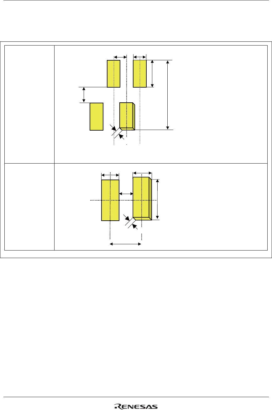
R61509V Target Spec
Rev. 0.11 April 25, 2008, page 36 of 181
Bump Arrangement
㪪
㪪㪈䌾㪪㪎㪉㪇䋬㩷
㪞㪈䌾㪞㪋㪊㪉䋬㩷
㪛㪬㪤㪤㪰㪩㪎㪄㪈㪇㪃㩷
㪫㪜㪪㪫㪦㪈㪈㪄㪈㪏㪃㩷
㪭㪞㪣㪛㪤㪰㪈㪄㪋㩷
㩷
㩷
㩷
㩷
㩷
㩷
㩷
㩷
㩷
㩷
㩷
㩷
㩷
㩷
㩷
㩷
㩷
㩷
㩷
㩷
㪠㪆㪦㩷㫇㫀㫅㫊㩷
㩿㪥㫆㪈㩷㵨㩷㪉㪍㪉㪀
㩷
㩷
Unit : um
S=1,500um
2
15
15
100
19
90
50
70
Unit : um
S=4,500um
2
20
219
12
12
50
㩿㪥㫆㩷㪉㪍㪊㪄㪈㪋㪊㪋㪀
Figure 3
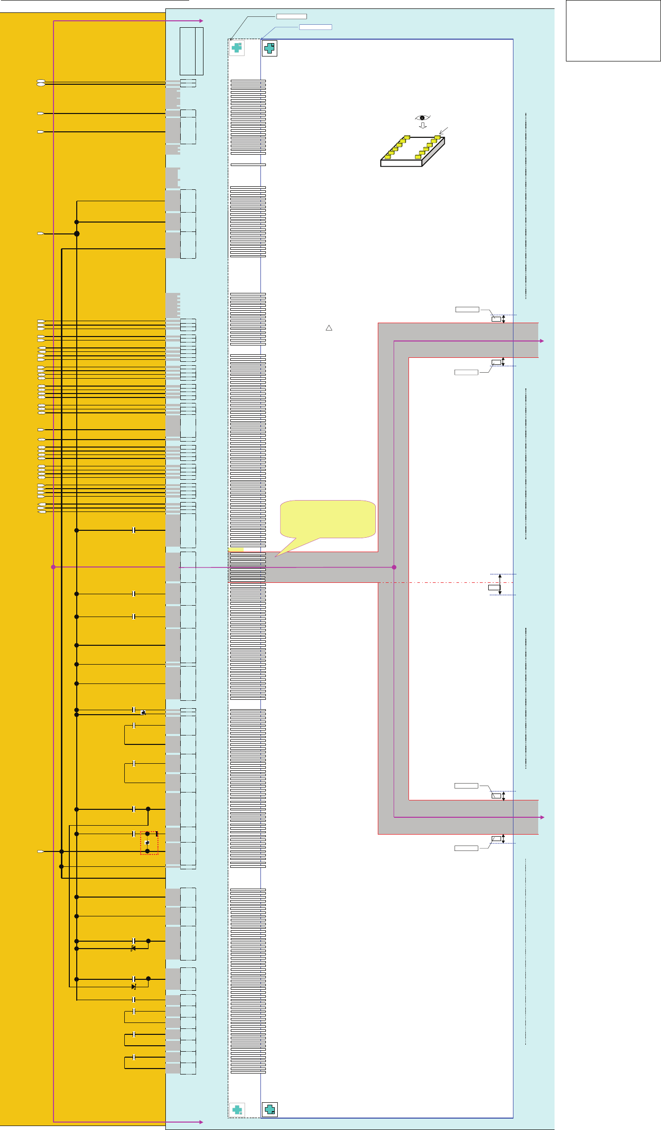
R61509V Wiring Example & Recommended Wiring Resistance (Pad Arrangement Rev0.6) 2008.04.21 Rev0.5
VCOM
R61509V Pad name
□DUMMYR4
1DUMMYR1 □DUMMYR3
2DUMMYR2 □TESTO15
3AGNDDUM1 □VGLDMY4
4 VPP3B Connect to AGNDDUM1/2 □G1
5 VPP3B Connect to AGNDDUM1/2 □G3
6 VPP3B Connect to AGNDDUM1/2 □G5
7 VPP3B Connect to AGNDDUM1/2 □G7
8AGNDDUM2 □G9
VPP3A p 9 VPP3A
10 VPP3A
11 VPP1
12 VPP1
13 VPP1
VPP1 p 14 VPP1
15 VPP1
16 VPP1
17 VPP1
18 GNDDUM1
19 VDDTEST Connect to GNDDUM1
20 VREFC Connect to GNDDUM1
21 VREFD □ Open
22 VREF □ Open
23 VCCDUM1
24 DUMMYA □ Open
25 DUMMYA □ Open
26 DUMMYA □ Open
27 DUMMYA □ Open
28 DUMMYA □ Open
29 GNDDUM2
30 AGND
31 AGND
32 AGND
33 AGND
34 AGND
35 AGND
36 GND
37 GND
38 GND
39 GND
40 GND
GND p 41 VCC
42 VCC
43 VCC
44 VCC
45 VCC
46 VCC
47 VCC
48 TS8 □ Open
49 TS7 □ Open
50 TS6 □ Open
51 TS5 □ Open
52 TS4 □ Open
53 TS3 □ Open
54 TS2 □ Open
55 TS1 □ Open
56 TS0 □ Open
57 TEST5 Connect to GNDDUM3
58 TEST4 Connect to GNDDUM3
59 TEST3 Connect to GNDDUM3 □ G427
60 TEST2 Connect to GNDDUM3 □ G429
61 TEST1 Connect to GNDDUM3 □ G431
62 GNDDUM3 □VGLDMY3
63 TSC Connect to GNDDUM3
IM2 in 60 64 IM2 Connect to IOVCCDUM1/GNDDUM3
IM1 in 60 65 IM1 Connect to IOVCCDUM1/GNDDUM3
IM0 in 60 66 IM0_ID Connect to IOVCCDUM1/GNDDUM3
67 IOVCCDUM1 VCOM
PROTECT in 60 68 PROTECT
RESX in 60 69 RESETX
60 70 GNDDUM4
LEDON out 60 71 DUMMYB □ Open
LEDPWM out 60 72 DUMMYB □ Open
VSYNC in 60 73 VSYNCX
HSYNC in 60 74 HSYNCX
75 IOVCCDUM2
DE in 60 76 ENABLE □ TESTO14
PCLK in 60 77 DOTCLK □S1
DB17 io 60 78 DB17 □S2
DB16 io 60 79 DB16 □S3
80 GNDDUM5 □S4
DB15 io 60 81 DB15 □S5
DB14 io 60 82 DB14
DB13 io 60 83 DB13
DB12 io 60 84 DB12
85 GNDDUM6
DB11 io 60 86 DB11
DB10 io 60 87 DB10
DB9 io 60 88 DB9
89 IOVCC
90 IOVCC
91 IOVCC
IOVCC p 92 IOVCC
(MIPI name: VDDI) 93 IOVCC
94 IOVCC
DB8 io 60 95 DB8
96 GNDDUM7
DB7 io 60 97 DB7
DB6 io 60 98 DB6
DB5 io 60 99 DB5
DB4 io 60 100 DB4
101 GNDDUM8
DB3 io 60 102 DB3
DB2 io 60 103 DB2
DB1 io 60 104 DB1
DB0 io 60 105 DB0
106 GNDDUM9
CSX in 60 107 CSX
DCX in 60 108 RS
WRX/SCL in 60 109 WRX_SCL
RDX in 60 110 RDX
111 GNDDUM10
TE out 60 112 FMARK
DIN in 60 113 SDI
DOUT out 60 114 SDO
115 VDD
116 VDD
1uF/6V/B 117 VDD
118 VDD
119 VDD
120 VDD
121 VDD
122 VDD □ S356
123 VDD □ S357
124 VMON □ Open □ S358
125 VCOM □ S359
126 VCOM □ S360
127 VCOM □ TESTO13
128 VCOM □ TESTO12
129 VCOM □ TESTO11
130 VCOM □ TESTO10
131 VCOM
132 VCOM
133 VCOMH
1uF/6V/B 134 VCOMH
135 VCOMH
136 VCOMH □ TESTO9
137 VCOMH □ TESTO8
138 VCOMH □ TESTO7
139 VCOML □ TESTO6
1uF/6V/B 140 VCOML □ S361
141 VCOML □ S362
142 VCOML □ S363
143 VCOML □ S364
144 VCOML □ S365
145 GND
146 GND
147 GND
148 GND
149 GND
150 GND
151 GND
152 GND
153 GND
60 154 VGS
155 AGND
156 AGND
157 AGND
158 AGND
159 AGND
160 AGND
161 AGND
162 AGND
163 AGND
1uF/6V/B 164 VTEST □ Open
165 VCIR □ Open
60 166 VREG1OUT
60 167 VCOMR
> 200kΩ168 C11M
169 C11M
170 C11M
171 C11M
1uF/6V/B 172 C11M
173 C11P
174 C11P
175 C11P
176 C11P
177 C11P
1uF/6V/B 178 C12M
179 C12M
180 C12M
181 C12M
182 C12M □ S716
183 C12P □ S717
184 C12P □ S718
185 C12P □ S719
186 C12P □ S720
187 C12P □ TESTO5
188 DDVDH
189 DDVDH
1uF/6V/B 190 DDVDH
191 DDVDH
192 DDVDH VCOM
193 DDVDH
194 DDVDH
195 DDVDH
196 DDVDH
197 VCI1
198 VCI1
199 VCI1
1uF/6V/B 200 VCI1
201 VCI □ VGLDMY2
0ohm 202 VCI □ G432
VCI p 203 VCI □ G430
(MIPI name: VDDI) 204 VCI □ G428
205 VCI
206 VCI
60 207 VCILVL
208 DUMMYC □ Open
209 DUMMYC □ Open
210 DUMMYC □ Open
211 DUMMYC □ Open
212 DUMMYC □ Open
213 GND
214 GND
215 GND
216 GND
217 GND
218 AGND
219 AGND
220 AGND
221 AGND
222 AGND
223 VGL
224 VGL
1uF/25V/B 225 VGL
226 VGL
227 VGL
228 VGL
229 VGL
VF<0.38V/5mA@25℃, VR≧25V 230 VGL
231 VGL
232 AGNDDUM3
233 AGNDDUM4
234 VGH
1uF/25V/B 235 VGH
236 VGH
237 VGH
238 VGH
239 VGH
VF<0.38V/5mA@25℃, VR≧25V 240 AGNDDUM5
241 VCL
242 VCL
1uF/6V/B 243 VCL
244 C13M
245 C13M
246 C13M
1uF/6V/B 247 C13P
248 C13P
249 C13P
250 C21M
251 C21M
252 C21M
1uF/10V/B 253 C21P
254 C21P
255 C21P □G10
256 C22M □G8
257 C22M □G6
258 C22M □G4
1uF/10V/B 259 C22P □G2
260 C22P □ VGLDMY1
261 C22P □ TESTO4
262 TESTO1 □ Open □ TESTO3
□TESTO2
FPC VCOM
Glass substrate
When VCOMH is adjusted
using variable resisrance
When VCI1 is adjusted by register
Capacitor is not required when VCI voltage is directly applied to VCI1 pin
30
10
10
8
7
7
9
8
7
10
10
12
20
20
20
10
20
20
20
20
12
12
Pad No.
Recommended
max.Rcog [ohm]
6
6
15
7
12
12
12
12
Chip
BUMP
Top View
TP
TP
30um
30um
30um
30um
30um_Space
30um_Space
30um_Space
840um
30um_Space
1
R61517 outline
R61509V outline
Rev0.1 2008.02.14 Made for PR
Rev0.11 2008.02.19 VPP3C-->VPP3B, VPP2-->VPP1
Rev0.2 2008.02.28 Pad names changed.
Rev0.3 2008.0314 Instruction changed.
Rev0.4 2008.0402 R61517's EEPROM IF deleted.
R61509V VPP2--> VPP1
Rev0.5 2008.04.21 Pad names changed.
Pad No66 IM0/ID→IM0_ID
Pad No69 RESET→RESETX
Pad No73 VSYNC→VSYNCX
Pad No74 HSYNC→HSYNCX
Pad No107 CS→CSX
Pad No109 WR/SCL→WRX_SCL
Pad No110 RD→RDX
Note: When using same glass substrate for the R61517 and
the R61509V, make sure that the R61517's VCOMA and
VCOMB for VCOM drive mode are same polarity.
The R61509V does not have VCOM output pin on the output
side (the area is just flat surface). When supplying voltage to
panel from four corners of it, draw wires from VCOM pins on the
I/O side.
R61509V Target Spec
Rev. 0.11 April 25, 2008, page 38 of 181
GRAM Address Map
Table 11 GRAM address and display position on the panel (SS = 0, BGR = 0)
S/G pin
S1
S2
S3
S4
S5
S6
S7
S8
S9
S10
S11
S12
・・・・・
S709
S710
S711
S712
S713
S714
S715
S716
S717
S718
S719
S720
GS=0 GS=1 WD[17:0] WD[17:0] WD[17:0] WD[17:0] ・・・・・ WD[17:0] WD[17:0] WD[17:0] WD[17:0]
G1 G432 h00000 h00001 h00002 h00003
・・・・・ h000EC h000ED h000EE h000EF
G2 G431 h00100 h00101 h00102 h00103 ・・・・・ h001EC h001ED h001EE h001EF
G3 G430 h00200 h00201 h00202 h00203
・・・・・ h002EC h002ED h002EE h002EF
G4 G429 h00300 h00301 h00302 h00303 ・・・・・ h003EC h003ED h003EE h003EF
G5 G428 h00400 h00401 h00402 h00403
・・・・・ h004EC h004ED h004EE h004EF
G6 G427 h00500 h00501 h00502 h00503
・・・・・ h005EC h005ED h005EE h005EF
G7 G426 h00600 h00601 h00602 h00603
・・・・・ h006EC h006ED h006EE h006EF
G8 G425 h00700 h00701 h00702 h00703
・・・・・ h007EC h007ED h007EE h007EF
G9 G424 h00800 h00801 h00802 h00803
・・・・・ h008EC h008ED h008EE h008EF
G10 G423 h00900 h00901 h00902 h00903
・・・・・ h009EC h009ED h009EE h009EF
G11 G422 h00A00 h00A01 h00A02 h00A03
・・・・・ h00AEC h00AED h00AEE h00AEF
G12 G421 h00B00 h00B01 h00B02 h00B03
・・・・・ h00BEC h00BED h00BEE h00BEF
G13 G420 h00C00 h00C01 h00C02 h00C03 ・・・・・ h00CEC h00CED h00CEE h00CEF
G14 G419 h00D00 h00D01 h00D02 h00D03
・・・・・ h00DEC h00DED h00DEE h00DEF
G15 G418 h00E00 h00E01 h00E02 h00E03 ・・・・・ h00EEC h00EED h00EEE h00EEF
G16 G417 h00F00 h00F01 h00F02 h00F03
・・・・・ h00FEC h00FED h00FEE h00FEF
G17 G416 h01000 h01001 h01002 h01003
・・・・・ h010EC h010ED h010EE h010EF
G18 G415 h01100 h01101 h01102 h01103
・・・・・ h011EC h011ED h011EE h011EF
G19 G414 h01200 h01201 h01202 h01203
・・・・・ h012EC h012ED h012EE h012EF
G20 G413 h01300 h01301 h01302 h01303
・・・・・ h013EC h013ED h013EE h013EF
: : : : : : : : : :
: : : : : : : : : :
G417 G16 h1A000 h1A001 h1A002 h1A003
・・・・・ h1A0EC h1A0ED h1A0EE h1A0EF
G418 G15 h1A100 h1A101 h1A102 h1A103
・・・・・ h1A1EC h1A1ED h1A1EE h1A1EF
G419 G14 h1A200 h1A201 h1A202 h1A203
・・・・・ h1A2EC h1A2ED h1A2EE h1A2EF
G420 G13 h1A300 h1A301 h1A302 h1A303 ・・・・・ h1A3EC h1A3ED h1A3EE h1A3EF
G421 G12 h1A400 h1A401 h1A402 h1A403
・・・・・ h1A4EC h1A4ED h1A4EE h1A4EF
G422 G11 h1A500 h1A501 h1A502 h1A503
・・・・・ h1A5EC h1A5ED h1A5EE h1A5EF
G423 G10 h1A600 h1A601 h1A602 h1A603
・・・・・ h1A6EC h1A6ED h1A6EE h1A6EF
G424 G9 h1A700 h1A701 h1A702 h1A703
・・・・・ h1A7EC h1A7ED h1A7EE h1A7EF
G425 G8 h1A800 h1A801 h1A802 h1A803
・・・・・ h1A8EC h1A8ED h1A8EE h1A8EF
G426 G7 h1A900 h1A901 h1A902 h1A903
・・・・・ h1A9EC h1A9ED h1A9EE h1A9EF
G427 G6 h1AA00 h1AA01 h1AA02 h1AA03
・・・・・ h1AAEC h1AAED h1AAEE h1AAEF
G428 G5 h1AB00 h1AB01 h1AB02 h1AB03
・・・・・ h1ABEC h1ABED h1ABEE h1ABEF
G429 G4 h1AC00 h1AC01 h1AC02 h1AC03 ・・・・・ h1ACEC h1ACED h1ACEE h1ACEF
G430 G3 h1AD00 h1AD01 h1AD02 h1AD03
・・・・・ h1ADEC h1ADED h1ADEE h1ADEF
G431 G2 h1AE00 h1AE01 h1AE02 h1AE03 ・・・・・ h1AEEC h1AEED h1AEEE h1AEEF
G432 G1 h1AF00 h1AF01 h1AF02 h1AF03
・・・・・ h1AFEC h1AFED h1AFEE h1AFEF
R61509V Target Spec
Rev. 0.11 April 25, 2008, page 39 of 181
Table 12 GRAM address and display position on the panel (SS = 1, BGR = 1)
S/G pin
S720
S719
S718
S717
S716
S715
S714
S713
S712
S711
S710
S709
・・・・・
S12
S11
S10
S9
S8
S7
S6
S5
S4
S3
S2
S1
GS=0 GS=1 WD[17:0] WD[17:0] WD[17:0] WD[17:0] ・・・・・ WD[17:0] WD[17:0] WD[17:0] WD[17:0]
G1 G432 h00000 h00001 h00002 h00003 ・・・・・ h000EC h000ED h000EE h000EF
G2 G431 h00100 h00101 h00102 h00103
・・・・・ h001EC h001ED h001EE h001EF
G3 G430 h00200 h00201 h00202 h00203 ・・・・・ h002EC h002ED h002EE h002EF
G4 G429 h00300 h00301 h00302 h00303
・・・・・ h003EC h003ED h003EE h003EF
G5 G428 h00400 h00401 h00402 h00403
・・・・・ h004EC h004ED h004EE h004EF
G6 G427 h00500 h00501 h00502 h00503
・・・・・ h005EC h005ED h005EE h005EF
G7 G426 h00600 h00601 h00602 h00603
・・・・・ h006EC h006ED h006EE h006EF
G8 G425 h00700 h00701 h00702 h00703
・・・・・ h007EC h007ED h007EE h007EF
G9 G424 h00800 h00801 h00802 h00803
・・・・・ h008EC h008ED h008EE h008EF
G10 G423 h00900 h00901 h00902 h00903
・・・・・ h009EC h009ED h009EE h009EF
G11 G422 h00A00 h00A01 h00A02 h00A03 ・・・・・ h00AEC h00AED h00AEE h00AEF
G12 G421 h00B00 h00B01 h00B02 h00B03 ・・・・・ h00BEC h00BED h00BEE h00BEF
G13 G420 h00C00 h00C01 h00C02 h00C03 ・・・・・ h00CEC h00CED h00CEE h00CEF
G14 G419 h00D00 h00D01 h00D02 h00D03 ・・・・・ h00DEC h00DED h00DEE h00DEF
G15 G418 h00E00 h00E01 h00E02 h00E03 ・・・・・ h00EEC h00EED h00EEE h00EEF
G16 G417 h00F00 h00F01 h00F02 h00F03 ・・・・・ h00FEC h00FED h00FEE h00FEF
G17 G416 h01000 h01001 h01002 h01003
・・・・・ h010EC h010ED h010EE h010EF
G18 G415 h01100 h01101 h01102 h01103
・・・・・ h011EC h011ED h011EE h011EF
G19 G414 h01200 h01201 h01202 h01203
・・・・・ h012EC h012ED h012EE h012EF
G20 G413 h01300 h01301 h01302 h01303
・・・・・ h013EC h013ED h013EE h013EF
: : : : : : : : : :
: : : : : : : : : :
G417 G16 h1A000 h1A001 h1A002 h1A003 ・・・・・ h1A0EC h1A0ED h1A0EE h1A0EF
G418 G15 h1A100 h1A101 h1A102 h1A103 ・・・・・ h1A1EC h1A1ED h1A1EE h1A1EF
G419 G14 h1A200 h1A201 h1A202 h1A203 ・・・・・ h1A2EC h1A2ED h1A2EE h1A2EF
G420 G13 h1A300 h1A301 h1A302 h1A303 ・・・・・ h1A3EC h1A3ED h1A3EE h1A3EF
G421 G12 h1A400 h1A401 h1A402 h1A403 ・・・・・ h1A4EC h1A4ED h1A4EE h1A4EF
G422 G11 h1A500 h1A501 h1A502 h1A503 ・・・・・ h1A5EC h1A5ED h1A5EE h1A5EF
G423 G10 h1A600 h1A601 h1A602 h1A603 ・・・・・ h1A6EC h1A6ED h1A6EE h1A6EF
G424 G9 h1A700 h1A701 h1A702 h1A703 ・・・・・ h1A7EC h1A7ED h1A7EE h1A7EF
G425 G8 h1A800 h1A801 h1A802 h1A803 ・・・・・ h1A8EC h1A8ED h1A8EE h1A8EF
G426 G7 h1A900 h1A901 h1A902 h1A903 ・・・・・ h1A9EC h1A9ED h1A9EE h1A9EF
G427 G6 h1AA00 h1AA01 h1AA02 h1AA03 ・・・・・ h1AAEC h1AAED h1AAEE h1AAEF
G428 G5 h1AB00 h1AB01 h1AB02 h1AB03 ・・・・・ h1ABEC h1ABED h1ABEE h1ABEF
G429 G4 h1AC00 h1AC01 h1AC02 h1AC03 ・・・・・ h1ACEC h1ACED h1ACEE h1ACEF
G430 G3 h1AD00 h1AD01 h1AD02 h1AD03 ・・・・・ h1ADEC h1ADED h1ADEE h1ADEF
G431 G2 h1AE00 h1AE01 h1AE02 h1AE03 ・・・・・ h1AEEC h1AEED h1AEEE h1AEEF
G432 G1 h1AF00 h1AF01 h1AF02 h1AF03 ・・・・・ h1AFEC h1AFED h1AFEE h1AFEF

R61509V Target Spec
Rev. 0.11 April 25, 2008, page 40 of 181
Instruction
Outline
The R61509V adopts 18-bit bus architecture in order to interface to high-performance microcomputer in
high speed. The R61509V starts internal processing after storing control information (18, 16, 9, 8, 1 bit(s)),
sent from the microcomputer, in the instruction register (IR) and the data register (DR). Since the internal
operation of the R61509V is controlled by the signals sent from the microcomputer, the register selection
signal (RS), the read/write signal (R/W), and the internal 16-bit data bus signals (IB15 ~ IB0) are called
instructions. The following are the kinds of instruction of the R61509V.
1. Specify index
2. Display control
3. Power management control
4. Set internal GRAM addresssss
5. Transfer data to and from the internal GRAM
6. Window address control
7. γ-correction
8. Panel Display Control
Normally, the data write instructions (5) are used the most frequently. The internal GRAM address is
updated automatically as data is written to the internal GRAM, which, in combination with the window
address function, contributes to minimizing data transfer and thereby lessens the load on the microcomputer.
The R61509V writes instructions consecutively by executing the instruction within the cycle when it is
written (instruction execution time: 0 cycle).
Instruction Data Format
As the following figure shows, the data bus used to transfer 16 instruction bits (IB[15:0]) is different
according to the data format of a selected interface. Make sure to transfer the instruction bits according to
the format of the selected interface.
The bits to which no instruction is assigned must be set to either “0” or “1” according to the following
register tables. When changing only one instruction bit setting, the setting values in other bits in the
register must be written.
R61509V Target Spec
Rev. 0.11 April 25, 2008, page 41 of 181
Index (IR)
R/W RS IB15 IB14 IB13 IB12 IB11 IB10 IB9 IB8 IB7 IB6 IB5 IB4 IB3 IB2 IB1 IB0
W 0 0 0 0 0 0 ID
[10]
ID
[9]
ID
[8]
ID
[7]
ID
[6]
ID
[5]
ID
[4]
ID
[3]
ID
[2]
ID
[1]
ID
[0]
The index register specifies the indexes of control register or RAM control to be accessed. It is prohibited
to access registers and instruction bits to which no index register is assigned.
Display control
Device code read (R000h)
R/W RS IB15 IB14 IB13 IB12 IB11 IB10 IB9 IB8 IB7 IB6 IB5 IB4 IB3 IB2 IB1 IB0
R 1 1 0 1 1 0 1 0 1 0 0 0 0 1 0 0 1
The device code “B509”H is read out when this register is read forcibly.
Driver Output Control (R001h)
R/W RS IB15 IB14 IB13 IB12 IB11 IB10 IB9 IB8 IB7 IB6 IB5 IB4 IB3 IB2 IB1 IB0
R/W 1 0 0 0 0 0 SM 0 SS 0 0 0 0 0 0 0 0
Default value 0 0 0 0 0 0 0 0 0 0 0 0 0 0 0 0
SS: Sets the shift direction of output from the source driver.
When SS = “0”, the source driver output shift from S1 to S720.
When SS = “1”, the source driver output shift from S720 to S1.
The combination of SS and BGR settings determines the RGB assignment to the source driver pins S1 ~
S720.
When SS = “0” and BGR = “0”, RGB dots are assigned one to one from S1 to S720.
When SS = “1” and BGR = “1”, RGB dots are assigned one to one from S720 to S1.
When changing the SS and BGR bits, RAM data must be rewritten.
SM: Controls the scan mode in combination with GS setting. See “ Scan mode setting”.
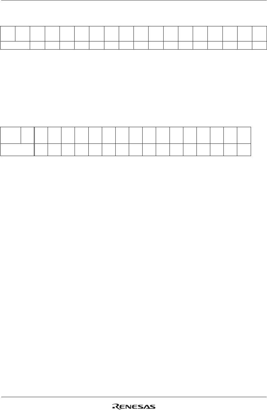
R61509V Target Spec
Rev. 0.11 April 25, 2008, page 42 of 181
LCD Drive Wave Control (R002h)
R/W RS IB15 IB14 IB13 IB12 IB11 IB10 IB9 IB8 IB7 IB6 IB5 IB4 IB3 IB2 IB1 IB0
R/W 1 0 0 0 0 0 0 0 BC 0 0 0 0 0 0 0 0
Default value 0 0 0 0 0 0 0 0 0 0 0 0 0 0 0 0
BC: Selects the liquid crystal drive waveform VCOM.
BC = 0: frame inversion waveform is selected.
BC = 1: line inversion waveform is selected.
Entry Mode (R003h)
The entry mode registers include instruction bits for setting how to write data from the microcomputer to
the internal GRAM of the R61509V.
AM: Sets either horizontal or vertical direction in updating the address counter automatically as the
R61509V writes data to the internal GRAM.
AM = “0”, sets the horizontal direction.
AM = “1”, sets the vertical direction.
When specifying window address area, the data is written only within the area in the direction determined
by ID and AM bits.
ID[1:0]: Either increments (+1) or decrements (-1) the address counter (AC) automatically as the data is
written to the GRAM. The ID[0] bit sets either increment or decrement in horizontal direction (updates the
address AD[7:0]). The ID[1] bit sets either increment or decrement in vertical direction (updates the
address AD[8:16]). The AM bit sets either horizontal or vertical direction in updating RAM address
counter automatically when writing data to the internal RAM.
ORG: Moves the origin address according to the ID setting when a window address area is described. This
function is enabled when executing burst data transfer within the window address area.
ORG = 0: The origin address is not moved. In this case, specify the address to start write
operation according to the GRAM address map within the window address area.
ORG = 1: The origin address “h00000” is moved according to the ID[1:0] setting.
Notes: 1. When ORG = 1, the origin address can be set only at “h00000”.
2. In RAM read operation, make sure to set ORG = 0.
R/W RS IB15 IB14 IB13 IB12 IB11 IB10 IB9 IB8 IB7 IB6 IB5 IB4 IB3 IB2 IB1 IB0
R/W 1 TRI
DF
M 0 BGR 0 0 0 0 OR
G 0 ID
[1]
ID
[0] AM 0 0 0
Default value 0 0 0 0 0 0 0 0 0 0 1 1 0 0 0 0

R61509V Target Spec
Rev. 0.11 April 25, 2008, page 43 of 181
BGR: Reverses the order from RGB to BGR in writing 18-bit pixel data in the GRAM.
BGR = 0: Write data in the order of RGB to the GRAM.
BGR = 1: Reverse the order from RGB to BGR in writing data to the GRAM.
DFM: In combination with the TRI setting, DFM sets the format to develop 16-/8-bit data to 18-bit data
when using either 16- or 8-bit bus interface. Make sure to set DFM = 0 when not transferring data via 16-
bit or 8-bit interface. Set DFM in accordance with selected interface and image data format in RAM write
operation.
DFM=0: 18bpp (R:G:B = 6:6:6), DFM=1: 16bpp (R:G:B = 5:6:5)
TRI: Selects the format to transfer data bits via 16-bit or 8-bit interface.
In 8-bit interface operation,
TRI = 0: 16-bit RAM data is transferred in two transfers.
TRI = 1: 18-bit RAM data is transferred in three transfers.
In 16-bit bus interface operation,
TRI = 0: 16-bit RAM data is transferred in one transfer.
TRI = 1: 18-bit RAM data is transferred in two transfers.
Make sure TRI = 0 when not transferring data via 16- or 8-bit interface. Also, set TRI = 0 during read
operation.
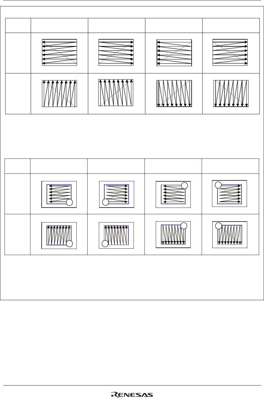
R61509V Target Spec
Rev. 0.11 April 25, 2008, page 44 of 181
ORG = 0
AM = 0
Horizontal
AM = 1
Vertical
ID1-0 = 00
Horizontal: Decrement
Vertical: Decrement
ID1-0 = 01
Horizontal: Increment
Vertical: Decrement
ID1-0 = 10
Horizontal: Decrement
Vertical: Increment
ID1-0 = 11
Horizontal: Increment
Vertical: Increment
17'h00000
17'hAFEF
17'h00000 17'h00000
17'h00000 17'h0000017'h00000
17'h00000 17'h00000
S S
SS
S S
SS
ORG = 1
AM = 0
Horizontal
AM = 1
Vertical
ID1-0 = 00
Horizontal: Decrement
Vertical: Decrement
ID1-0 = 01
Horizontal: Increment
Vertical: Decrement
ID1-0 = 10
Horizontal: Decrement
Vertical: Increment
ID1-0 = 11
Horizontal: Increment
Vertical: Increment
17'h00000
17'h00000 17'h00000
17'h00000 17'h00000
17'h00000
17'h00000 17'h00000
17'hAFEF
17'hAFEF 17'hAFEF 17'hAFEF
17'hAFEF 17'hAFEF 17'hAFEF
17'hAFEF 17'hAFEF 17'hAFEF 17'hAFEF
17'hAFEF 17'hAFEF 17'hAFEF 17'hAFEF
Automatic Address Update (ORG = 0, AM, ID)
Note: When writing data within the window address area with ORG = 0,
any address within the window address area can be set as the starting point of data write operation.
Automatic Address Update (ORG = 1, AM, ID)
Notes: 1. When ORG = 1, the address to start data write operation within the window address area is set
at either corner of the window address area (the positions of the S in the circle in the above figure).
2. When ORG = 1, make sure to set the address h00000 in the RAM address set register.
Setting other addresses is prohibited.
Figure 4 Automatic Address Update

R61509V Target Spec
Rev. 0.11 April 25, 2008, page 45 of 181
Display Control 1 (R007h)
BASEE: Base image display enable bit.
BASEE = 0: No base image is displayed. The R61509V drives the LCD at non-lit display level or displays
partial images.
BASEE = 1: A base image is displayed.
PTDE: Partial display 1 enable bit.
PTDE=0: Partial display is turned off. Only a base image is displayed on the panel.
PTDE=1: Partial image is displayed. Set BASEE = 0 to turn off the base image.
R/W RS IB15 IB14 IB13 IB12 IB11 IB10 IB9 IB8 IB7 IB6 IB5 IB4 IB3 IB2 IB1 IB0
R/W 1 0 0 0
PTD
E 0 0 0
BAS
EE 0 0 0 0 0 0 0 0
Default 0 0 0 0 0 0 0 0 0 0 0 0 0 0 0 0
R61509V Target Spec
Rev. 0.11 April 25, 2008, page 46 of 181
Display Control 2 (R008h)
FP[7:0]: Sets the number of lines for front porch period (a blank period made after the end of display).
BP[7:0]: Sets the number of lines for back porch period (a blank period made before the beginning of
display).
In external display interface operation, a back porch (BP) period starts on the falling edge of the VSYNCX
signal and the display operation starts after the back porch period. After the front porch period, a blank
period continues until next VSYNCX input is detected.
Table 13
FP [7:0]
BP [7:0] Number of front porch line Number of back porch line
8’h00 Setting inhibited Setting inhibited
8’h01 Setting inhibited Setting inhibited
8’h02 Setting inhibited 2 lines
8’h03 3 lines 3 lines
8’h04 4 lines 4 lines
8’h05 5 lines 5 lines
8’h06 6 lines 6 lines
8’h07 7 lines 7 lines
8’h08 8 lines 8 lines
8’h09 9 lines 9 lines
8’h0A 10 lines 10 lines
8’h0B 11 lines 11 lines
8’h0C 12 lines 12 lines
8’h0D 13 lines 13 lines
8’h0E 14 lines 14 lines
8’h0F 15 lines 15 lines
: : :
8’h7F 127 lines 127 lines
8’h80 128 lines 128 lines
8’h81 Setting inhibited Setting inhibited
: : :
8’hFF Setting inhibited Setting inhibited
R/W RS IB15 IB14 IB13 IB12 IB11 IB10 IB9 IB8 IB7 IB6 IB5 IB4 IB3 IB2 IB1 IB0
R/W 1 FP
[7]
FP
[6]
FP
[5]
FP
[4]
FP
[3]
FP
[2]
FP
[1]
FP
[0]
BP
[7]
BP
[6]
BP
[5]
BP
[4]
BP
[3]
BP
[2]
BP
[1]
BP
[0]
Default 0 0 0 0 1 0 0 0 0 0 0 0 1 0 0 0
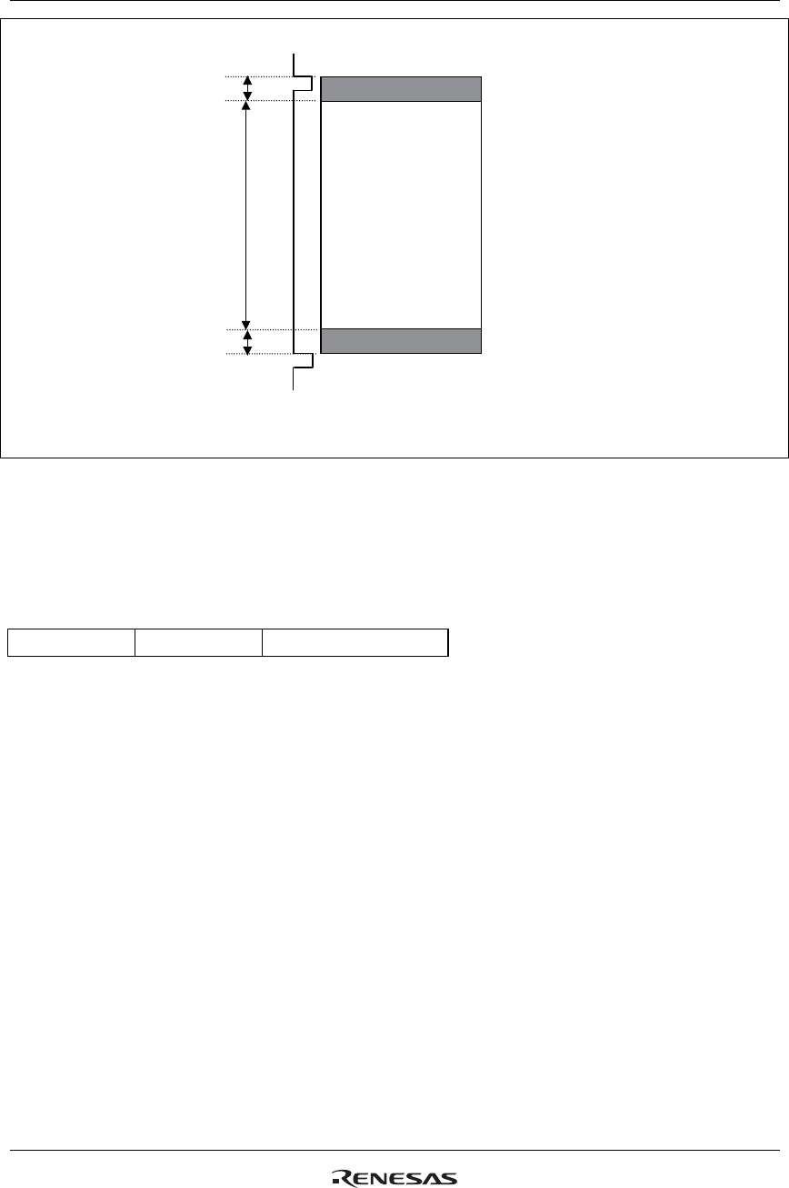
R61509V Target Spec
Rev. 0.11 April 25, 2008, page 47 of 181
VSYNCX
NL
BP
FP
Back porch
Front porch
Display Area
Note: The output timing to the panel is delayed by 2 line period
from the synchronous signal (VSYNCX) input.
Figure 5 Front and Back Porch Periods
Note on Setting BP and FP:
Set the BP and FP bits as follows in the following operation modes, respectively.
Table 14
BP ≥ 2 lines FP ≥ 3 lines FP + BP ≤ 256 lines
R61509V Target Spec
Rev. 0.11 April 25, 2008, page 48 of 181
Display Control 3 (R009h)
PTS: Sets the source output level to drive non-display area. PTS also selects operation of grayscale
amplifier and step-up clock frequency.
Table 15
Source output in non-lit display area (Note) Non-lit display area
Step-up clock frequency
PTS
Positive polarity Negative polarity
Grayscale amplifier
in operation
0 V63 V0 V0 to V63 Register setting (DC0, DC1)
1 V63 V0 V0, V63 Register setting (DC0) x 1/2
Note: The power efficiency improved by halting grayscale amplifiers and slowing down the step-up clock
frequency can be obtained in non-display drive period.
PTV: Sets the VCOM output in non-lit display area. When PTV=1, frame inversion in non-lit display area
is selected.
Table 16
PTV VCOM operation in non-lit display drive period
0 BC setting
1 Frame inversion
R/W RS IB15 IB14 IB13 IB12 IB11 IB10 IB9 IB8 IB7 IB6 IB5 IB4 IB3 IB2 IB1 IB0
R/W 1 0 0 0 0 PTV PTS 0 0 0 0 0 0 0 0 0 0
Default 0 0 0 0 0 0 0 0 0 0 0 0 0 0 0 1
R61509V Target Spec
Rev. 0.11 April 25, 2008, page 49 of 181
8 Color Control (R00Bh)
R/W RS IB15 IB14 IB13 IB12 IB11 IB10 IB9 IB8 IB7 IB6 IB5 IB4 IB3 IB2 IB1 IB0
W/R 1 0 0 0 0 0 0 0 0 0 0 0 0 0 0 0 COL
Default value 0 0 0 0 0 0 0 0 0 0 0 0 0 0 0 0
COL: When COL = 1, the R61509V enters the eight-color display mode. RAM data rewrite operation is
not required when setting the eight-color display mode. Set the 8-color mode instruction according to the
8-color mode sequence.
The electrical potential of liquid crystal drive in 8-color display mode is V0/V63. Selecting frame inversion
is recommended to reduce power consumption.
Table 17
COL Display Color
1’h0 262,144 colors
1’h 1 8 colors
R61509V Target Spec
Rev. 0.11 April 25, 2008, page 50 of 181
External Display Interface Control 1 (R00Ch)
RIM: Sets the interface format when RGB interface is selected by RM and DM bits. Set RIM bit before
starting display operation via the external display interface. Do not change the setting while the R61509V
performs display operation.
Table 18
RIM RGB interface operation Color
0 18-bt RGB interface (1 transfer/pixel) DB17-0 262,144
1 16-bit RGB interface (1 transfer / pixel) DB17-13, 11-1 65536
Notes: 1: Instruction bits are set via system interface.
2: Transfer the RGB dot data one by one in synchronization with DOTCLK.
DM[1:0]: The DM[1:0] setting allows switching between internal clock operation mode and external
display interface operation mode. However, switching between the RGB interface operation and the
VSYNCX interface operation is prohibited.
Table 19 Display Interface
DM[1:0] Display Interface
2’h0 Internal clock operations
2’h1 RGB interface
2’h2 VSYNC interface
2’h3 Setting inhibited
RM: Selects the interface for RAM access operation. RAM access is possible only via the interface
selected by the RM bit. Set RM = 1 when writing display data via RGB interface. When RM = 0, it is
possible to write data via system interface while performing display operation via RGB interface.
Table 20 RAM Access Interface
RM RAM Access Interface
0 System interface/VSYNC interface
1 RGB interface * Transfer instruction commands via clock synchronous serial interface.
R/W RS IB15 IB14 IB13 IB12 IB11 IB10 IB9 IB8 IB7 IB6 IB5 IB4 IB3 IB2 IB1 IB0
R/W 1 0 ENC
[2]
ENC
[1]
ENC
[0] 0 0 0 RM 0 0
DM
[1]
DM
[0] 0 0 0 RIM
Default 0 0 0 0 0 0 0 0 0 0 0 0 0 0 0 0

R61509V Target Spec
Rev. 0.11 April 25, 2008, page 51 of 181
ENC[2:0]: Sets the RAM write cycle via RGB interface.
Table 21
ENC[2:0] RAM Write Cycle (frame periods)
3’h0 1 frame
3’h1 2 frames
3’h2 3 frames
3’h3 4 frames
3’h4 5 frames
3’h5 6 frames
3’h6 7 frames
3’h7 8 frames
R61509V Target Spec
Rev. 0.11 April 25, 2008, page 52 of 181
External Display Interface Control 2 (R00Fh)
R/W RS IB15 IB14 IB13 IB12 IB11 IB10 IB9 IB8 IB7 IB6 IB5 IB4 IB3 IB2 IB1 IB0
R/W 1 0 0 0 0 0 0 0 0 0 0 0 VSPL HSPL 0 EPL DPL
Default value 0 0 0 0 0 0 0 0 0 0 0 0 0 0 0 0
DPL: Sets the signal polarity of DOTCLK pin.
DPL = 0: input data on the rising edge of DOTCLK
DPL = 1: input data on the falling edge of DOTCLK
EPL: Sets the signal polarity of ENABLE pin.
EPL = 0: writes data DB17-0 when ENABLE = “0” and disables data write operation
when ENABLE = “1”.
EPL = 1: writes data DB17-0 when ENABLE = “1” and disables data write operation
when ENABLE = “0”.
HSPL: Sets the signal polarity of HSYNCX pin.
HSPL = 0: low active
HSPL = 1: high active
VSPL: Sets the signal polarity of VSYNCX pin.
VSPL = 0: low active
VSPL = 1: high active
R61509V Target Spec
Rev. 0.11 April 25, 2008, page 53 of 181
Panel Interface Control 1 (R010h)
RTNI[4:0]: Sets 1H (line) period. This setting is valid when the R61509V’s display operation is
synchronized with internal clock signal.
Table 22 Clocks per Line (Internal Clock Operation)
RTNI[4:0] Clocks per Line RTNI[4:0] Clocks per Line
5’h00-5’h0F Setting inhibited 5’h18 24 clocks
5’h10 16 clocks 5’h19 25 clocks
5’h11 17 clocks 5’h1A 26 clocks
5’h12 18 clocks 5’h1B 27 clocks
5’h13 19 clocks 5’h1C 28 clocks
5’h14 20 clocks 5’h1D 29 clocks
5’h15 21 clocks 5’h1E 30 clocks
5’h16 22 clocks 5’h1F 31 clocks
5’h17 23 clocks
Note: In Power Supply Instruction Setting, Deep Standby Exit Sequence and Sleep Mode Exit Sequence,
RTNI bit must be set at the “Initial instruction setting” state. See “Power Supply Setting Sequence”
and “Instruction Setting Sequence and Refresh Sequence”.
DIVI[1:0]: Sets the division ratio of the internal clock frequency. The R61509V’s internal operation is
synchronized with the frequency divided internal clock, which is set according to the division ratio
determined by DIVI[1:0] setting. The frame frequency can be changed by setting RTNI and DIVI bits.
When changing the number of lines to drive the LCD panel, adjust the frame frequency too. For details,
see Frame-Frequency Adjustment Function.
In RGB interface operation, the DIVI[1:0] setting has no effect.
Table 23 Division Ratio (Internal Operation)
DIVI[1:0] Division Ratio Internal Operation Clock Unit
2’h0 1/1 1 x OSC
2’h1 1/2 2 x OSC
2’h2 1/4 4 x OSC
2’h3 1/8 8 x OSC
Note: In Power Supply Instruction Setting, Deep Standby Exit Sequence and Sleep Mode Exit Sequence,
RTNI bit must be set at the “Initial instruction setting” state. See “Power Supply Setting Sequence”
and “Instruction Setting Sequence and Refresh Sequence”.
R/W RS IB15 IB14 IB13 IB12 IB11 IB10 IB9 IB8 IB7 IB6 IB5 IB4 IB3 IB2 IB1 IB0
R/W 1 0 0 0 0 0 0
DIV
I
[1]
DIV
I
[0]
0 0 0
RTNI
[4]
RTNI
[3]
RTNI
[2]
RTNI
[1]
RTNI
[0]
Default 0 0 0 0 0 0 0 0 0 0 0 1 1 0 0 1

R61509V Target Spec
Rev. 0.11 April 25, 2008, page 54 of 181
Frame Frequency Calculation
fosc
Frame frequency = Clocks per line x division ratio x (line + BP + FP) [Hz]
fosc : RC oscillation frequency
Line: Number of lines to drive the LCD (NL bits)
Division ratio: DIVI
Clocks per line: RTNI
R61509V Target Spec
Rev. 0.11 April 25, 2008, page 55 of 181
Panel Interface Control 2 (R011h)
R/W RS IB15 IB14 IB13 IB12 IB11 IB10 IB9 IB8 IB7 IB6 IB5 IB4 IB3 IB2 IB1 IB0
R/W 1 0 0 0 0 0
NOW
I[2]
NOW
I[1]
NOW
I[0] 0 0 0 0 0
SDTI
[2]
SDTI
[1]
SDTI
[0]
Default 0 0 0 0 0 0 0 1 0 0 0 0 0 0 0 1
NOWI[2:0]: Sets the non-overlap period of adjacent gate outputs. The setting is enabled when the
R61509V’s display operation is synchronized with internal clock signals.
Table 24
NOWI[2:0] Non-overlap period NOWI[2:0] Non-overlap period
3'h0 0 (internal clock *see note) 3'h4 4 (internal clock
*see note)
3'h1 1 3'h5 5
3'h2 2 3'h6 6
3'h3 3 3'h7 7
Note: The internal clock is the frequency divided clock, which is set by DIVI[[1:0] bits.
SDTI[2:0]: Sets the source output delay period from the reference point. For the relationships between
gate interface signals, see Liquid Crystal Panel Interface Timing.
Table 25
SDTI[2:0] Source output delay period
3’h0 0 clocks
3’h1 1 clock
3’h2 2 clocks
3’h3 3 clocks
3’h4 4 clocks
3’h5 5 clocks
3’h6 6 clocks
3’h7 7 clocks
Notes: 1. The number of clocks in the table setting is measured from the reference point.
2. 1 clock = (internal oscillation clock (OSC1) period) x (division ratio)
3. The reference point is the falling edge of gate output.
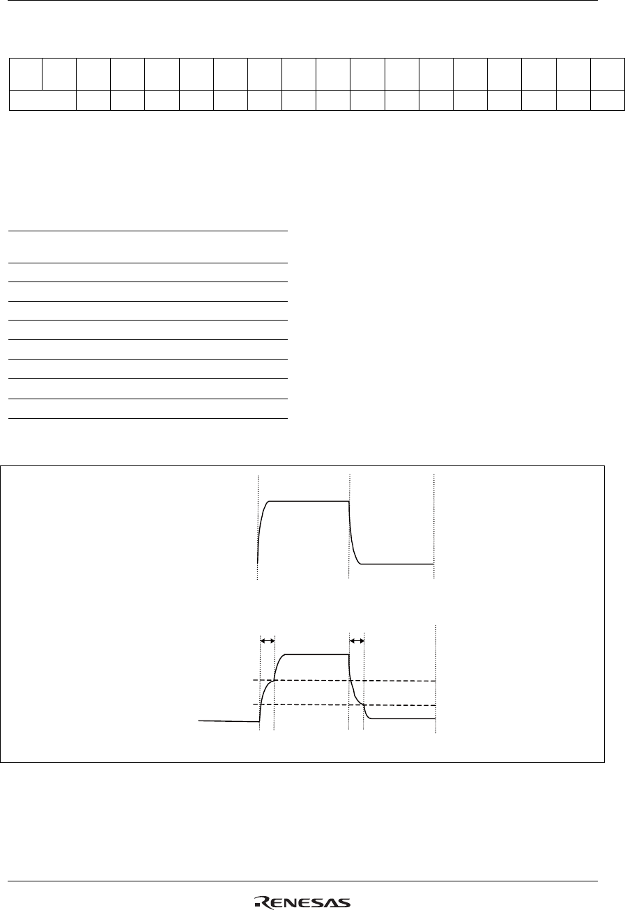
R61509V Target Spec
Rev. 0.11 April 25, 2008, page 56 of 181
Panel Interface Control 3 (R012h)
R/W RS IB15 IB14 IB13 IB12 IB11 IB10 IB9 IB8 IB7 IB6 IB5 IB4 IB3 IB2 IB1 IB0
R/W 1 0 0 0 0 0
VEQ
WI[2]
VEQ
WI[1]
VEQ
WI[0] 0 0 0 0 0
SEQ
WI[2]
SEQ
WI[1]
SEQ
WI[0]
Default value 0 0 0 0 0 0 0 0 0 0 0 0 0 0 0 0
VEQWI[2:0]: Sets VCOM equalize period. The VCOM equalize operation is executed from VCOM
alternating point defined by MCPI [2:0] for the period defined by VEQWI [2:0]. This function is disabled
when RGB interface is selected.
Table 26
VEQWI [2:0] VCOM Equalize period
3’h0 0 clocks
3’h1 1 clock
3’h2 2 clocks
3’h3 3 clocks
3’h4 4 clocks
3’h5 5 clocks
3’h6 6 clocks
3’h7 7 clocks
Note: The clock is the frequency divided clock, which is set by DIVI[[1:0] bits.
㪭㪚㪦㪤㩷㫆㫌㫋㫇㫌㫋
㩷
㩷
㪭㪜㪨㪮㪠㪲㪉㪑㪇㪴
㪞㪥㪛㩷㫃㪼㫍㪼㫃㩷
㪭㪜㪨㪮㪠㪲㪉㪑㪇㪴
㪭㪚㪠㩷㫃㪼㫍㪼㫃㩷 㩷
1) VEQW [2:0]=0h
㪭㪚㪦㪤㩷㫆㫌㫋㫇㫌㫋
2) VEQWI [2:0]
≠0h
Figure 6
R61509V Target Spec
Rev. 0.11 April 25, 2008, page 57 of 181
SEQWI[2:0]: Sets source equalize period. SEQWI setting is enabled only when the R61509V executes
display operation in synchronization with internal clock.
Table 27
SEQWI[2:0] Source Equalize Period
3'h0 0 clocks
3'h1 1 clock
3'h2 2 clocks
3'h3 3 clocks
3'h4 4 clocks
3'h5 5 clocks
3'h6 6 clocks
3'h7 7 clocks
Note: The clock is the frequency divided clock, which is set by DIVI[[1:0] bits.
R61509V Target Spec
Rev. 0.11 April 25, 2008, page 58 of 181
Panel Interface Control 4 (R013h)
MCPI: Defines VCOM alternating timing. This bit is enabled when displaying in synchronization with
internal clock. MCP cannot be used in RGB interface operation.
Table 28
MCPI [2:0] VCOM alternating timing
3’h0 Setting inhibited
3’h1 1 clock
3’h2 2 clocks
3’h3 3 clocks
3’h4 4 clocks
3’h5 5 clocks
3’h6 6 clocks
3’h7 7 clocks
Note: The clock is the frequency divided clock, which is set by DIVI [1:0] bits.
R/W RS IB15 IB14 IB13 IB12 IB11 IB10 IB9 IB8 IB7 IB6 IB5 IB4 IB3 IB2 IB1 IB0
R/W 1 0 0 0 0 0 0 0 0 0 0 0 0 0
MC
PI[2]
MC
PI
[1]
MC
PI
[0]
Default 0 0 0 0 0 0 0 0 0 0 0 0 0 0 0 1
R61509V Target Spec
Rev. 0.11 April 25, 2008, page 59 of 181
Panel Interface Control 5 (R014h)
PCDIVH[2:0], PCDIVL[2:0]: When DM=1 and RGB I/F is selected, display operation is executed using
DOTCLKD. PCDIVH and PCDIVL define division ratio of DOTCLK to generate DOTCLKD.
PCDIVH is used to define number of DOTCLK in High period in units of one clock.
PCDIVL is used to define number of DOTCLK in Low period in units of one clock.
Make sure that PCDIVL=PCDIVH or PCDIVH-1.
Write PCDIVH and PCDIVL values so that DOTCLKD frequency is the closest to internal oscillation
clock frequency 678KHz.
For details, see “Setting Example of Display Control Clock in RGB Interface Operation”.
Table 29 Table 30
PCDIVH[2:0] Number of DOTCLK
in High period
PCDIVL[2:0] Number of DOTCLK
in Low period
3’h0 Setting inhibited 3’h0 Setting inhibited
3’h1 1 clock 3’h1 1 clock
3’h2 2 clocks 3’h2 2 clocks
3’h3 3 clocks 3’h3 3 clocks
3’h4 4 clocks 3’h4 4 clocks
3’h5 5 clocks 3’h5 5 clocks
3’h6 6 clocks 3’h6 6 clocks
3’h7 7 clocks 3’h7 7 clocks
R/W RS IB15 IB14 IB13 IB12 IB11 IB10 IB9 IB8 IB7 IB6 IB5 IB4 IB3 IB2 IB1 IB0
R/W 1 0 0 0 0 0 0 0 0 0
PC
DIV
H
[2]
PC
DIV
H
[1]
PC
DIV
H
[0]
0
PC
DIV
L
[2]
PC
DIV
L
[1]
PC
DIV
L
[0]
Default 0 0 0 0 0 0 0 0 0 1 0 1 0 1 0 1
R61509V Target Spec
Rev. 0.11 April 25, 2008, page 60 of 181
Panel Interface Control 6 (R020h)
DIVE[1:0]: Sets the division ratio of DOTCLK. The R61509V’s internal operation is synchronized with
the frequency-divided DOTCLK, the frequency of which is divided by the division ratio set by DIVE[1:0].
This setting is enabled while the R61509V’s display operation is synchronized with RGB interface signals.
Table 31 Division Ratio of DOTCLK (RGB interface operation)
DIVE[1:0] Division ratio
2’h0 1/1
2’h1 1/2
2’h2 1/4
2’h3 1/8
Note: Clock frequency for internal operation = DOTCLK / (( DIVE x (PCDIVL + PCDIVH) ). For details, see
R014h.
R/W RS IB15 IB14 IB13 IB12 IB11 IB10 IB9 IB8 IB7 IB6 IB5 IB4 IB3 IB2 IB1 IB0
R/W 1 0 0 0 0 0 0
DIV
E[1]
DIV
E[0] 0 0] RTN
E[5]
RTN
E[4]
RTN
E[3]
RTN
E[2]
RTN
E[1]
RTN
E[0]
Default 0 0 0 0 0 0 0 0 0 0 0 1 1 0 0 1
R61509V Target Spec
Rev. 0.11 April 25, 2008, page 61 of 181
RTNE[5:0]: Sets RTNE in combination with PCDIVH and PCDIVL to decide the number of DOTCLK in
1H (1 line) period according to the following formula. RTNE is enabled when RGB interface is selected.
DOTCLKD x RTNE (Number of clock) ≤ DOTCLK in 1H period.
Table 32 DOTCLKD in 1H period (RGB interface operation)
RTNE[5:0] Clocks per
line period (1H) RTNE[5:0] Clocks per
line period (1H)
6'h00 Setting inhibited 6'h20 32 clocks
6'h01 Setting inhibited 6'h21 33 clocks
6'h02 Setting inhibited 6'h22 34 clocks
6'h03 Setting inhibited 6'h23 35 clocks
6'h04 Setting inhibited 6'h24 36 clocks
6'h05 Setting inhibited 6'h25 37 clocks
6'h06 Setting inhibited 6'h26 38 clocks
6'h07 Setting inhibited 6'h27 39 clocks
6'h08 Setting inhibited 6'h28 40 clocks
6'h09 Setting inhibited 6'h29 41 clocks
6'h0A Setting inhibited 6'h2A 42 clocks
6'h0B Setting inhibited 6'h2B 43 clocks
6'h0C Setting inhibited 6'h2C 44 clocks
6'h0D Setting inhibited 6'h2D 45 clocks
6'h0E Setting inhibited 6'h2E 46 clocks
6'h0F Setting inhibited 6'h2F 47 clocks
6'h10 16 clocks 6'h30 48 clocks
6'h11 17 clocks 6'h31 49 clocks
6'h12 18 clocks 6'h32 50 clocks
6'h13 19 clocks 6'h33 51 clocks
6'h14 20 clocks 6'h34 52 clocks
6'h15 21 clocks 6'h35 53 clocks
6'h16 22 clocks 6'h36 54 clocks
6'h17 23 clocks 6'h37 55 clocks
6'h18 24 clocks 6'h38 56 clocks
6'h19 25 clocks 6'h39 57 clocks
6'h1A 26 clocks 6'h3A 58 clocks
6'h1B 27 clocks 6'h3B 59 clocks
6'h1C 28 clocks 6'h3C 60 clocks
6'h1D 29 clocks 6'h3D 61 clocks
6'h1E 30 clocks 6'h3E 62 clocks
6'h1F 31 clocks 6'h3F 63 clocks
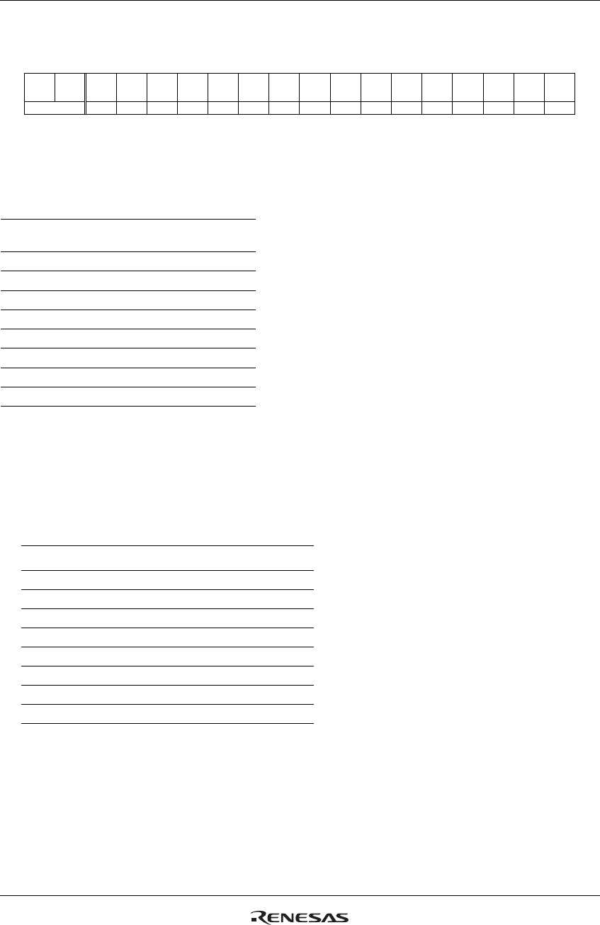
R61509V Target Spec
Rev. 0.11 April 25, 2008, page 62 of 181
Panel Interface Control 7 (R021h)
NOWE[2:0]: Sets the non-overlap period of adjacent gate outputs. NOWE is enabled when RGB interface
is selected.
Table 33
NOWE[2:0] Non-overlap period
3’h0 0 clocks
3’h1 1 clock
3’h2 2 clocks
3’h3 3 clocks
3’h4 4 clocks
3’h5 5 clocks
3’h6 6 clocks
3’h7 7 clocks
Note: 1 clock = (number of data transfer/pixel) x DIVE (division ratio) x (PCDIVL + PCDIVH) [DOTCLK]
SDTE[2:0]: Sets the source output delay period from the reference point when the R61509V’s display
operation is synchronized with DOTCLK (DM = 2’h1). For the relationships between signals, see Liquid
Crystal Panel Interface Timing.
Table 34
SDTE[2:0] Source output delay period
3’h0 0 clocks
3’h1 1 clock
3’h2 2 clocks
3’h3 3 clocks
3’h4 4 clocks
3’h5 5 clocks
3’h6 6 clocks
3’h7 7 clocks
Notes: 1. The number of clocks in the table setting is measured from the reference point.
2. 1 clock = DOTCLKD (when pixel data is transferred in one- transfer)
3. The reference point is falling edge of gate control signals.
R/W RS IB15 IB14 IB13 IB12 IB11 IB10 IB9 IB8 IB7 IB6 IB5 IB4 IB3 IB2 IB1 IB0
R/W 1 0 0 0 0 0
NOW
E[2]
NOW
E[1]
NOW
E[0] 0 0 0 0 0
SDTE
[2]
SDTE
[1]
SDTE
[0]
Default 0 0 0 0 0 0 0 1 0 0 0 0 0 0 0 1
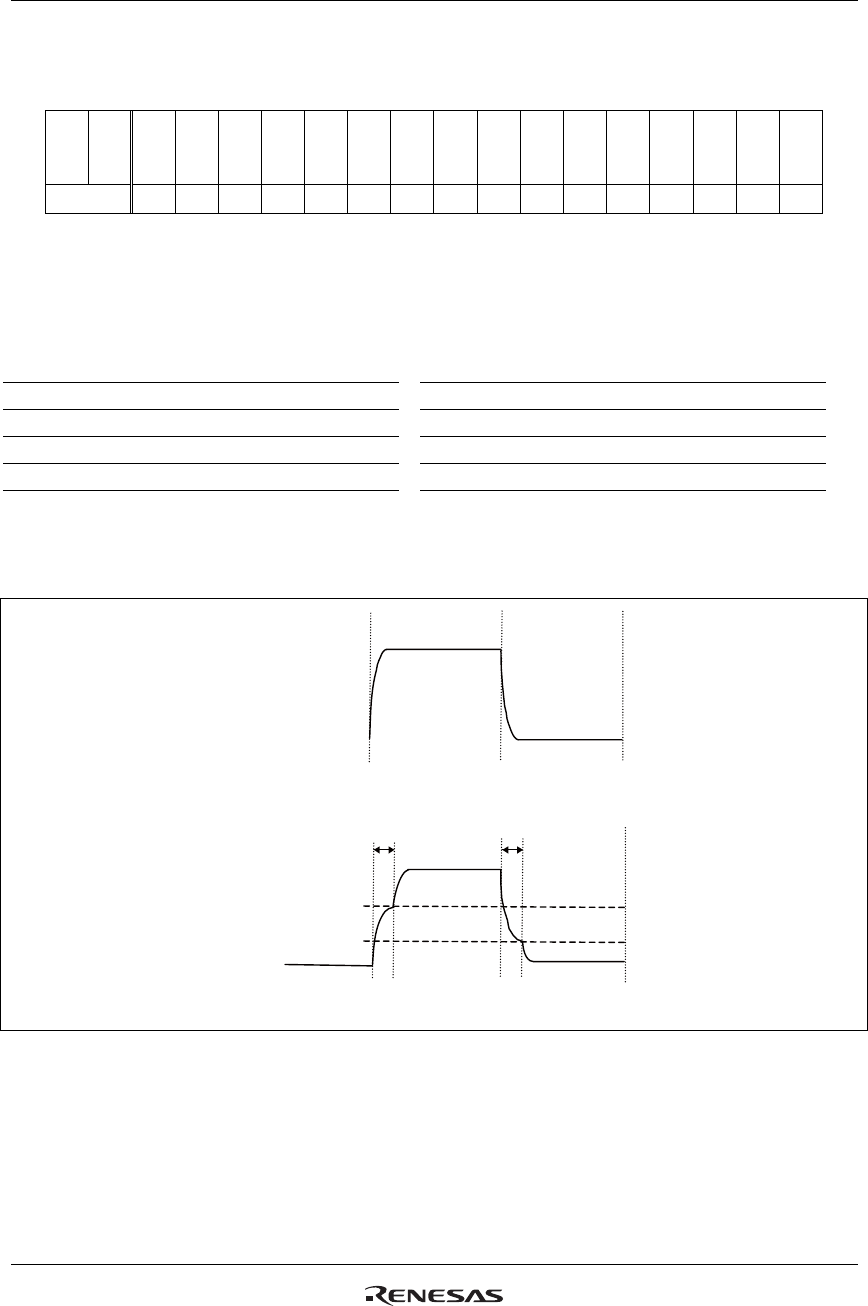
R61509V Target Spec
Rev. 0.11 April 25, 2008, page 63 of 181
Panel Interface Control 8 (R022h)
VEQWE[2:0]: Sets low power VCOM drive period. The setting is enabled when RGB interface is
selected.
Table 35
VEQWE[2:0] Source output delay period VEQWE[2:0] Source output delay period
3’h0 0 clocks (*see Notes) 3’h4 4 clocks
3’h1 1 clock 3’h5 5 clocks
3’h2 2 clocks 3’h6 6 clocks
3’h3 3 clocks 3’h7 7 clocks
Notes: 1. 1 clock
= (Number of data transfer/pixel) x DIVE (division ratio) x (PCDIVL + PCDIVH)) [DOTCLK]
2. The number of clocks is measured from the reference point. The reference point is the
alternating position of VCOM, which is set by SDTE bits.
㪭㪚㪦㪤㩷㫆㫌㫋㫇㫌㫋
㩷
㩷
㪭㪜㪨㪮㪠㪲㪉㪑㪇㪴
㪞㪥㪛㩷㫃㪼㫍㪼㫃㩷
㪭㪜㪨㪮㪠㪲㪉㪑㪇㪴
㪭㪚㪠㩷㫃㪼㫍㪼㫃㩷 㩷
1) VEQW [2:0]=0h
㪭㪚㪦㪤㩷㫆㫌㫋㫇㫌㫋
2) VEQWI [2:0] ≠0h
Figure 7
R/W RS IB15 IB14 IB13 IB12 IB11 IB10 IB9 IB8 IB7 IB6 IB5 IB4 IB3 IB2 IB1 IB0
R/W 1 0 0 0 0 0
VEQ
WE
[2]
VEQ
WE
[1]
VEQ
WE
[0]
0 0 0 0 0
SEQ
WE
[2]
SEQ
WE
[1]
SEQ
WE
[0]
Default 0 0 0 0 0 0 0 0 0 0 0 0 0 0 0 0
R61509V Target Spec
Rev. 0.11 April 25, 2008, page 64 of 181
SEQWE[2:0]: Sets source equalize period. SEQWE setting is enabled when the R61509V executes
display operation via RGB interface.
Table 36
SEQWE[2:0] Source Equalize Period
3'h0 0 clocks
3'h1 1 clock
3'h2 2 clocks
3'h3 3 clocks
3'h4 4 clocks
3'h5 5 clocks
3'h6 6 clocks
3'h7 7 clocks
Note: 1 clock = (number of data transfer/pixel) x DIVE(Division ratio) x (PCDIVL + PCDIVH)) [DOTCLK]
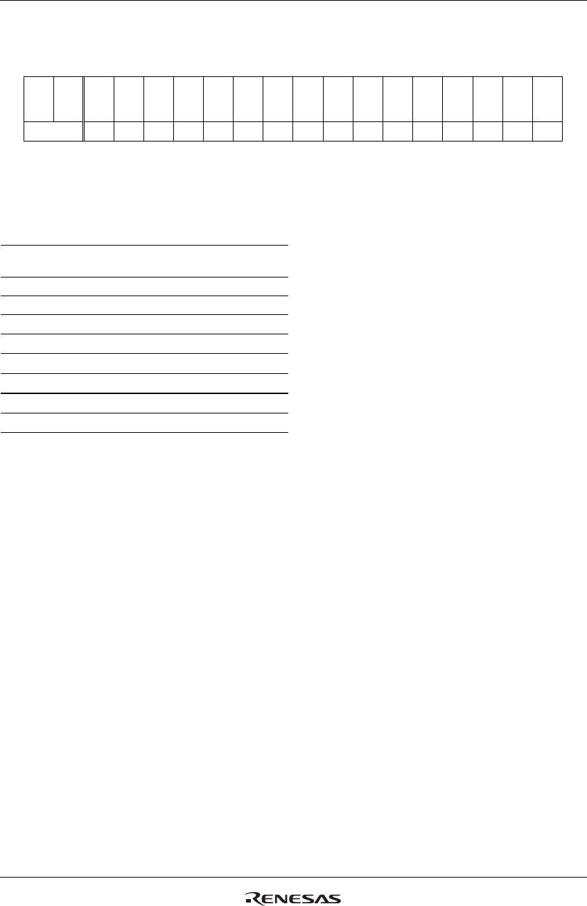
R61509V Target Spec
Rev. 0.11 April 25, 2008, page 65 of 181
Panel Interface Control 9 (R023h)
MCPE [2:0]: Specifies VCOM alternating point. MCPE is enabled when RGB interface is selected.
Table 37
MCPE [2:0] VCOM alternating point
3’h0 Setting inhibited
3’h1 1 clock
3’h2 2 clocks
3’h3 3 clocks
3’h4 4 clocks
3’h5 5 clocks
3’h6 6 clocks
3’h7 7 clocks
Note: 1 clock = (number of data transfer/pixel) x DIVE(Division ratio) x (PCDIVL + PCDIVH)) [DOTCLK]
R/W RS IB15 IB14 IB13 IB12 IB11 IB10 IB9 IB8 IB7 IB6 IB5 IB4 IB3 IB2 IB1 IB0
R/W 1 0 0 0 0 0 0 0 0 0 0 0 0 0
MC
PE
[2]
MC
PE
[1]
MC
PE
[0]
Default 0 0 0 0 0 0 0 0 0 0 0 0 0 0 0 1
R61509V Target Spec
Rev. 0.11 April 25, 2008, page 66 of 181
Frame Marker Control (R090h)
FMI[2:0]: Sets FMARK output interval by FMI register setting according to the update period of display
data and transfer rate. Set FMKM = 1 if FMARK signal is output from FMARK pin. See “FMARK
Interface” for detail.
Table 38
FMI[2] FMI[1] FMI[0] Output interval
0 0 0 1 frame
0 0 1 2 frames
0 1 1 4 frames
1 0 1 6 frames
Other settings Setting inhibited
FMP[8:0]: Sets the output position of frame synchronous signal (frame marker). A pulse (FMARK) is
output by starting from back porch during a 1H period when FMP[8:0] = 9’h000 (high active, amplitude:
IOVCC1-GND). FMP[8:0] is used as a trigger signal for write operation in synchronization with frame.
Setting range: 9’h000 ≤ FMP ≤ BP + NL + FP
For details, see “FMARK Interface”.
Table 39
R/W RS IB15 IB14 IB13 IB12 IB11 IB10 IB9 IB8 IB7 IB6 IB5 IB4 IB3 IB2 IB1 IB0
R/W 1 FM
KM
FMI
[2]
FMI
[1]
FMI
[0] 0 0 0
FMP
[8]
FMP
[7]
FMP
[6]
FMP
[5]
FMP
[4]
FMP
[3]
FMP
[2]
FMP
[1]
FMP
[0]
Default 0 0 0 0 0 0 0 0 0 0 0 0 0 0 0 0
FMP[8:0] FMARK output position
9’h000 0
9’h001 1
9’h002 2
:
9’h1BE 446
9’h1BF 447
9’h1C0 ~ 9’h1FF Setting inhibited
R61509V Target Spec
Rev. 0.11 April 25, 2008, page 67 of 181
Power Control
Power Control 1 (R100h)
DSTB: When DSTB = 1, the R61509V enters the shut down mode. In shut down mode, the internal logic
power supply is turned off to reduce power consumption. The GRAM data and instruction setting are not
maintained when the R61509V is in the shut down mode. Set the instruction again after the shut down
mode is exited. GND level is outputted to the panel in the shut down mode.
AP[1:0]: Adjusts the constant current in the operational amplifier circuit in the LCD power supply circuit.
The larger constant current, the better the drivability of the LCD, but it also increases the current
consumption. Adjust the constant current taking the trade-off between the display quality and the current
consumption into account. In no-display period, set AP[1:0]=2’h0 to halt operational amplifiers and step-
up circuits to reduce power consumption.
Table 40 Constant Current in Operational Amplifiers
AP[1:0] Electricity in LCD drive power supply amplifiers
2’h0 Operational amplifiers and step-up circuits halt
2’h1 0.5
2’h2 0.75
2’h3 1
Note: The values in the table represent the ratios of currents in respective settings to the current when
AP[1:0]=2’h3.
R/W RS IB15 IB14 IB13 IB12 IB11 IB10 IB9 IB8 IB7 IB6 IB5 IB4 IB3 IB2 IB1 IB0
R/W 1 0 0 0 0 0
BT
[2]
BT
[1]
BT
[0] 0 0
AP
[1]
AP
[0] 0 DST
B 0 0
Default 0 0 0 0 0 0 1 1 0 0 1 1 0 0 0 0
R61509V Target Spec
Rev. 0.11 April 25, 2008, page 68 of 181
BT[2:0]: Sets the factor used in the step-up circuits. Select the optimal step-up factor for the operating
voltage. To reduce power consumption, set a smaller factor.
Table 41 Step-Up Factor for Step-Up Circuits
BT[2:0] DDVDH VCL VGH VGL
3’h0 Setting inhibited
3’h1 -(VCI1+DDVDH x 2)
[x –5]
3’h2 -(DDVDH x 2)
[x –4]
3’h3
VCI1 x2
[x 2]
-VCI1
[x –1]
DDVDH x 3
[x 6]
-(VCI1+DDVDH)
[x –3]
3’h4 Setting inhibited
3’h5 -(VCI1+DDVDH x 2)
[x –5]
3’h6 -(DDVDH x 2)
[x –4]
3’h7
VCI1 x2
[x 2]
-VCI1
[x –1]
VCI1+DDVDH
x 2
[x 5]
-(VCI1+DDVDH)
[x –3]
Notes: 1. The factors in the brackets show the step-up factors from VCI1.
2. Make sure DDVDH=max.6.0V, VGH=max.18.0V, VGL=max -13.5V, VGH-VGL=max. 28.0V, and
VCL=max -3.0V.
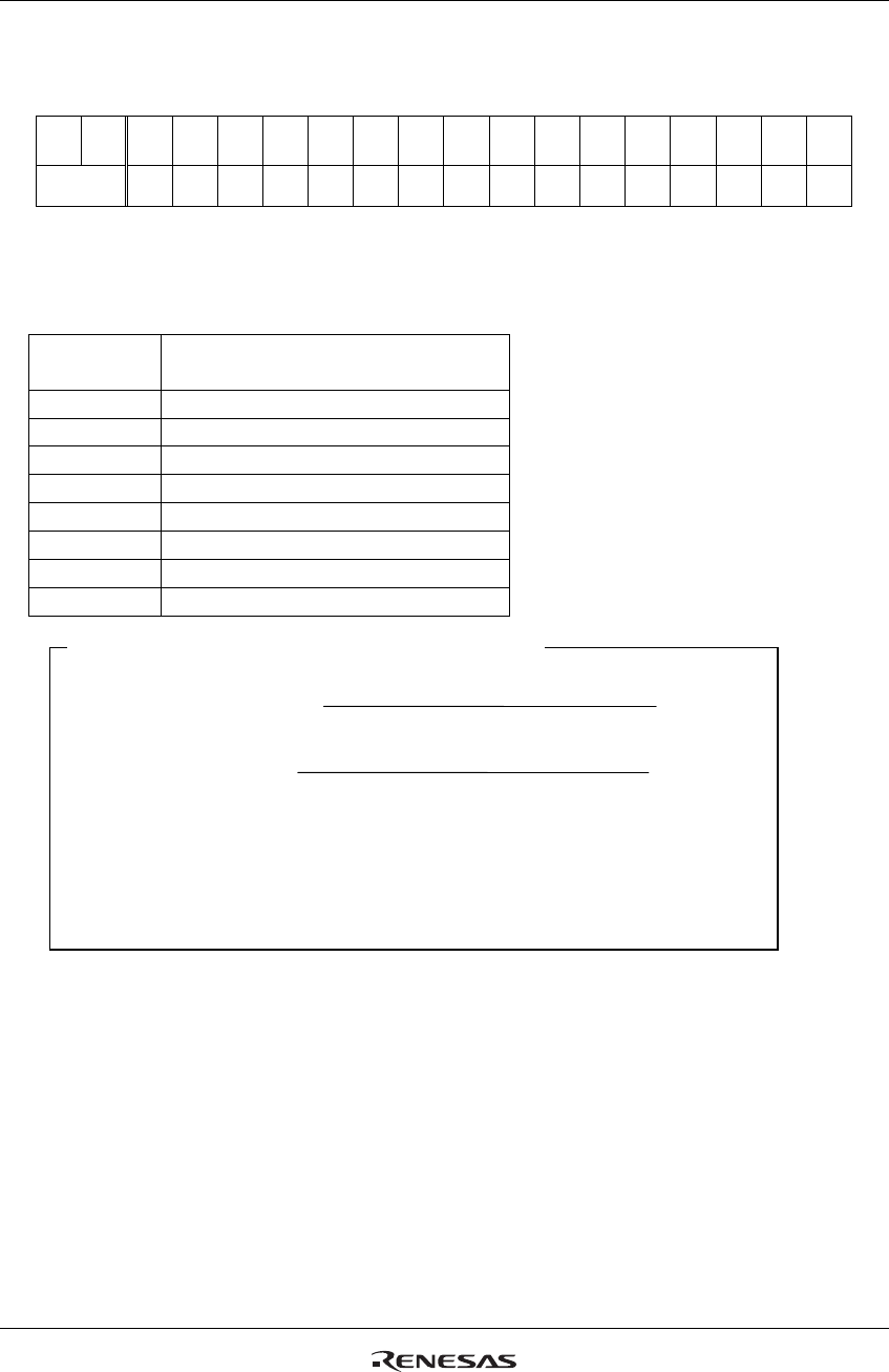
R61509V Target Spec
Rev. 0.11 April 25, 2008, page 69 of 181
Power Control 2 (R101h)
DC1 [2:0]: Sets step-up clock frequency for Step-up Circuit 2. The step-up clock is in synchronization
with internal clock.
Table 42 Step-up Frequency (Step-up Circuit 1)
DC1[2:0] Step-up Circuit 2
Step-up frequency (fDCDC2)
3’h0 Step-up Circuit 2 halts
3’h1 Setting inhibited
3’h2 Line frequency / 4
3’h3 Line frequency / 8
3’h4 Line frequency / 16
3’h5 Setting inhibited
3’h6 Setting inhibited
3’h7 Setting inhibited
R/W RS IB15 IB14 IB13 IB12 IB11 IB10 IB9 IB8 IB7 IB6 IB5 IB4 IB3 IB2 IB1 IB0
R/W 1 0 0 0 0 0
DC1
[2]
DC1
[1]
DC1
[0] 0 DC0
[2]
DC0
[1]
DC0
[0] 0 VC
[2]
VC
[1]
VC
[0]
Default 0 0 0 0 0 0 1 0 0 1 0 0 0 1 1 1
fosc : Internal clock frequency
N
umber of clock per line : RTN*[4:0] (RTNI or RTNE)
Division ratio : DIV*[1:0] (DIVI or DIVE)
N
: DC1 [2:0]
Step-up clock frequency (fDCDC2) =
Internal clock frequency fOSC
[
Hz
]
[Step-up clock frequency for Step-up Circuit 2]
Number of clock per line x Division ratio x 2(N)
Line fre
q
uenc
y
2(N)
=
[
Hz
]
R61509V Target Spec
Rev. 0.11 April 25, 2008, page 70 of 181
DC0 [2:0]: Sets step-up clock frequency for Step-up Circuit 1. The step-up clock is in synchronization
with internal clock.
Table 43 Step-up Frequency (Step-up Circuit 2)
Note 1: Make sure that fDCDC1 ≥fDCDC2.
Note 2: Set DC0 and RTN* so that ((DCDC1 step-up frequency) ≤(Line frequency). If not, step-up operation
may not be completed satisfactory.
The step-up frequencies synchronize with display operation. Clock count is reset at the beginning of 1H
period.
DC0[2:0] Step-up Circuit 1
Step-up frequency (fDCDC1)
3’h0 Step-up circuit 1 halts
3’h1 Setting inhibited
3’h2 Setting inhibited
3’h3 Setting inhibited
3’h4 FOSC / 8
3’h5 FOSC / 16
3’h6 FOSC / 32
3’h7 Setting inhibited
fosc : Internal clock frequency
Division ratio : DIV*[1:0] ((DIVI or DIVE)
N
: DC1 [2:0]
Step-up clock frequency (fDCDC1) =
Internal clock frequency fOSC
[
Hz
]
[Step-up clock frequency for Step-up Circuit 1]
Number of clock per line x Division ratio x 2(N-1)
Line fre
q
uenc
y
2(N-1)
=
[
Hz
]
R61509V Target Spec
Rev. 0.11 April 25, 2008, page 71 of 181
VC[2:0]: Sets VCI voltage level.
VC[2:0] VCI1 voltage (Reference voltage for step-up operation)
3’h0 Setting inhibited
3’h1 0.94 x VCILVL
3’h2 0.89 x VCILVL
3’h3 Setting inhibited
3’h4 Setting inhibited
3’h5 0.76 x VCILVL
3’h6 Setting inhibited
3’h7 1.00 x VCILVL
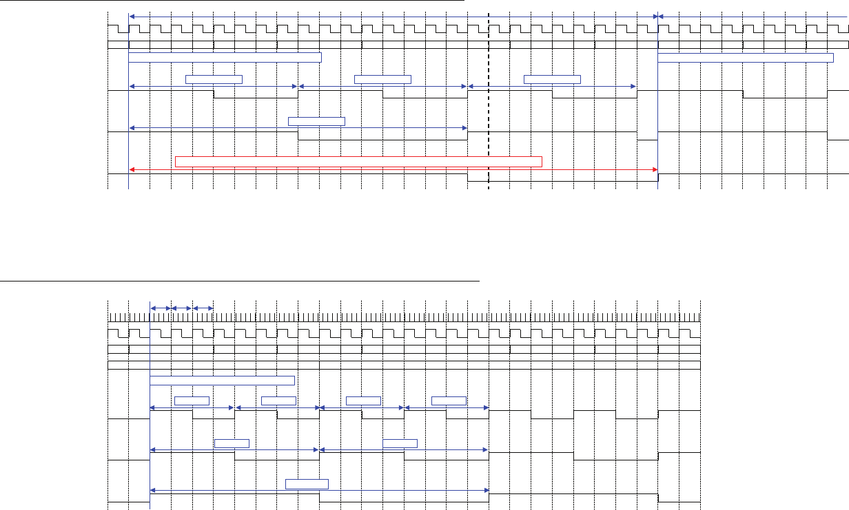
■DC0x Value and DCDC1 Step-up Clock Signal Waveform Example
DCDC1 performs charge operation and boost operation with the step-up clock generated from the timing generator.
The DCDC1 step-up clock frequency is adjusted by setting the division ratio of the reference clock frequency with DC0x register.
(To prevent flickering, the DCDC1 step-up clock signal is synchronized with the reference point of display operation in unit of lines.)
Note: Set DC0x and RTNx so that (DCDC1 step-up clock frequency) ≧ (line clock frequency)
If the above restriction is not followed, the duty cycle during the boost period is less than 50%. As a result, the step-up circuit may not operate normally.
Example) DIVn=2'h0, RTN=5'h19 (reference clock period = 1/1 of internal operation clock, 1H period = 25 clocks)
Reference point Reference point
Reference clock
Reference clock counter
a) DC0x=3'h4
(1/8 of reference clock frequency)
DCDC1 step-up clock
b) DC0x=3'h5
(1/16 of reference clock frequency)
DCDC1 step-up clock
c) DC0x=3'h6
(1/32 of reference clock frequency)
DCDC1 step-up clock
■DC1x Value and DCDC2 Step-up Clock Signal Waveform Example
DCDC2 performs charge operation and boost operation with the step-up clock generated from the timing generator.
The DCDC2 step-up clock frequency is adjusted by setting the division ratio of the reference clock frequency with DC1x register.
(To prevent flicker, the DCDC2 step-up clock signal is synchronized with the head of BP period in unit of lines.)
Example) BP=FP=8'h08, NL=7'h6B (front porch = back porch 8 lines, the number of lines to drive the LCD = 432 lines)
Reference Reference Reference Reference Reference Reference Reference Reference Reference Reference Reference Reference Reference Reference Reference Reference Reference Reference Reference Reference Reference Reference Reference Reference Reference Reference Reference Reference
point point point point point point point point point point point point point point point point point point point point point point point point point point point point
Reference clock
Line clock
Counter for the number of lines
Front Porch Back Porch Display Area
a) DC1x=3'h2
(1/4 of line clock frequency)
DCDC2 step-up clock
b) DC1x=3'h3
(1/8 of line clock frequency)
DCDC2 step-up clock
c) DC0x=3'h4
(1/16 of line clock frequency)
DCDC2 step-up clock
5'h085'h05 5'h06 5'h075'h01 5'h02 5'h03 5'h04
'h017 'h018 'h019'h1BE 'h013 'h014 'h015 'h016'h00F 'h010 'h011 'h012'h00B 'h00C 'h00D 'h00E'h007 'h008 'h009 'h00A'h003 'h004 'h005 'h006'h1BF 'h000 'h001 'h002
5'h18 5'h005'h10 5'h14 5'h15 5'h16 5'h175'h10 5'h11 5'h12 5'h135'h0C 5'h0D 5'h0E 5'h0F5'h08 5'h09 5'h0A 5'h0B5'h04 5'h05 5'h06 5'h075'h00 5'h01 5'h02 5'h03
Note: The duty cycle of the step-up clock should be close to 50%.
1H period
Synchronized with the reference point in unit of lines
Synchronized with the head of BP period
1H period 1H period 1H period
8 clock cycles
16 clock cycles
32 clock cycles (As the number of clocks per 1H period is less than 32, the duty cycle of the step-up clock is not 50%.
4H cycles
8H cycles
16H cycles
4H cycles 4H cycles 4H cycles
8H cycles
8 clock cycles
Synchronized with the reference point in unit of lines
8 clock cycles
R61509V Target Spec
Rev. 0.11 April 25, 2008, page 73 of 181
Power Control3 (R102h)
Note: True values of PSON and PON are not read when instruction read is executed.
PON, PSON: Turn power supply ON. PON and PSON must be written to power supply ON and start the
internal power supply operation. Follow power supply sequencer to set PON and PSON bits.
VCMR: Selects either external resistance (VCOMR pin) or internal electronic volume (VCM[4:0]) to set
the electrical potential of VCOMH. The internal electronic volume is set by VCM bits
Table 44
VCMR0[0] VCOMH Electrical Potential setting
0 VCOMR (externally supplied)
1 Internal electronic volume
VRH[3:0]: Sets the factor to generate VREG1OUT.
Table 45
Note: Write VC and VRH bits so that VREG1OUT ≤DDVDH-
0.5V.
R/W RS IB15 IB14 IB13 IB12 IB11 IB10 IB9 IB8 IB7 IB6 IB5 IB4 IB3 IB2 IB1 IB0
VRH
[4]
VRH
[3]
VRH
[2]
VRH
[1]
VRH
[0] 0 0
VCM
R 1 0 PSON PON 0 0 0 0
R/W 1
R/W R/W R/W R/W R/W R/W R/W W W
Default 0 0 0 0 0 0 0 1 1 0 0 0 0 0 0 0
VRH[4:0] VREG1OUT
5’h00 Halt (Hiz)
5’h01-5’h0F Setting inhibited
5’h10 VCIR x 1.600
5’h11 VCIR x 1.625
5’h12 VCIR x 1.650
5’h13 VCIR x 1.675
5’h14 VCIR x 1.700
5’h15 VCIR x 1.725
5’h16 VCIR x 1.750
5’h17 VCIR x 1.775
5’h18 VCIR x 1.800
5’h19 VCIR x 1.825
5’h1A VCIR x 1.850
5’h1B VCIR x 1.875
5’h1C VCIR x 1.900
5’h1D VCIR x 1.925
5’h1E VCIR x 1.950
5’h1F VCIR x 1.975
R61509V Target Spec
Rev. 0.11 April 25, 2008, page 74 of 181
Power Control 4 (R103h)
VDV[4:0]: Selects the factor of VREG1OUT to set the amplitude of VCOM alternating voltage from 0.70
to 1.32.
Table 46
VDV[4:0] VCOM amplitude VDV[4:0] VCOM amplitude
5’h0 VREG1OUT x 0.70 5’h10 VREG1OUT x 1.02
5’h1 VREG1OUT x 0.72 5’h11 VREG1OUT x 1.04
5’h2 VREG1OUT x 0.74 5’h12 VREG1OUT x 1.06
5’h3 VREG1OUT x 0.76 5’h13 VREG1OUT x 1.08
5’h4 VREG1OUT x 0.78 5’h14 VREG1OUT x 1.10
5’h5 VREG1OUT x 0.80 5’h15 VREG1OUT x 1.12
5’h6 VREG1OUT x 0.82 5’h16 VREG1OUT x 1.14
5’h7 VREG1OUT x 0.84 5’h17 VREG1OUT x 1.16
5’h8 VREG1OUT x 0.86 5’h18 VREG1OUT x 1.18
5’h9 VREG1OUT x 0.88 5’h19 VREG1OUT x 1.20
5’hA VREG1OUT x 0.90 5’h1A VREG1OUT x 1.22
5’hB VREG1OUT x 0.92 5’h1B VREG1OUT x 1.24
5’hC VREG1OUT x 0.94 5’h1C VREG1OUT x 1.26
5’hD VREG1OUT x 0.96 5’h1D VREG1OUT x 1.28
5’hE VREG1OUT x 0.98 5’h1E VREG1OUT x 1.30
5’hF VREG1OUT x 1.00 5’h1F VREG1OUT x 1.32
Note 1: Set VDV[4:0] so that VCOM amplitude becomes 6.0V or less.
Note 2: Set VCOML (VCOMH-VCOM amplitude) ≤ 0V.
R/W RS IB15 IB14 IB13 IB12 IB11 IB10 IB9 IB8 IB7 IB6 IB5 IB4 IB3 IB2 IB1 IB0
R/W 1 0 0 0
VDV
[4]
VDV
[3]
VDV
[2]
VDV
[1]
VDV
[0] 0 0 0 0 0 0 0 0
Default 0 0 0 0 0 0 0 0 0 0 0 0 0 0 0 0
R61509V Target Spec
Rev. 0.11 April 25, 2008, page 75 of 181
RAM Access
RAM Address Set (Horizontal Address) (R200h)
RAM Address Set (Vertical Address) (R201h)
AD[16:0]: Sets a GRAM address in the AC (Address Counter) which is automatically updated according to
the combination of AM, ID[1:0] settings as the R61509V writes data to the internal GRAM. Data can be
written consecutively without resetting the address in the AC. The address is not automatically updated
after reading data from the internal GRAM.
Note 1: In RGB interface operation (RM = “1”), the address AD16-0 is set in the address counter every
frame on the falling edge of VSYNCX.
Note 2: In internal clock operation and VSYNC interface operation (RM = “0”), the address AD16-0 is set
when executing the instruction.
Table 47 GRAM Address setting range
AD[16:0] GRAM Data Setting
17’h00000 – 17’h000EF Bitmap data on the first line
17’h00100 – 17’h001EF Bitmap data on the second line
17’h00200 – 17’h002EF Bitmap data on the third line
17’h00300 – 17’h003EF Bitmap data on the fourth line
17’h00400 – 17’h004EF Bitmap data on the fifth line
: :
17’h1AC00 – 17’h1ACEF Bitmap data on the 429th line
17’h1AD00 – 17’h1ADEF Bitmap data on the 430th line
17’h1AE00 – 17’h1AEEF Bitmap data on the 431st line
17’h1AF00 – 17’h1AFEF Bitmap data on the 432nd line
R/W RS IB15 IB14 IB13 IB12 IB11 IB10 IB9 IB8 IB7 IB6 IB5 IB4 IB3 IB2 IB1 IB0
R
200 R/W 1 0 0 0 0 0 0 0 0
AD
[7]
AD
[6]
AD
[5]
AD
[4]
AD
[3]
AD
[2]
AD
[1]
AD
[0]
Default 0 0 0 0 0 0 0 0 0 0 0 0 0 0 0 0
R
201 R/W 1 0 0 0 0 0 0 0
AD
[16]
AD
[15]
AD
[14]
AD
[13]
AD
[12]
AD
[11]
AD
[10]
AD
[9]
AD
[8]
Default 0 0 0 0 0 0 0 0 0 0 0 0 0 0 0 0
R61509V Target Spec
Rev. 0.11 April 25, 2008, page 76 of 181
GRAM Data Write (R202h)
R/W RS
W 1 RAM write data WD[17:0] is transferred via different data bus in different interface operation.
RGB
interface RAM write data WD[17:0] is transferred via different data bus in different interface operation.
WD[17:0]: The R61509V develops data into 18 bits internally in write operation. The format to develop
data into 18 bits is different in different interface operation.
The GRAM data represents the grayscale level. The R61509V automatically updates the address according
to AM and ID[1:0] settings as it writes data in the GRAM. The DFM bit sets the format to develop 16-bit
data into the 18-bit data in 16-bit or 8-bit interface operation.
Note: When writing data in the GRAM via system interface while using the RGB interface, make sure
that write operations via two interfaces that do not conflict one another.
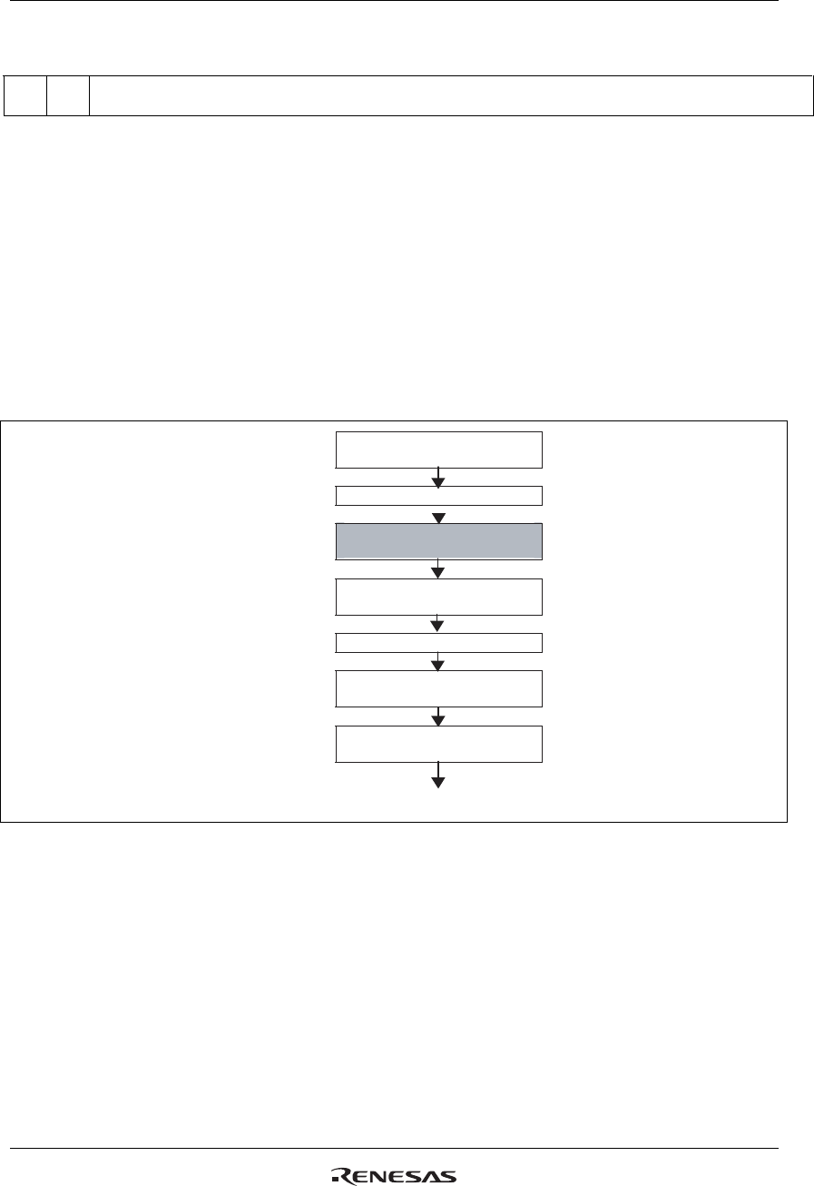
R61509V Target Spec
Rev. 0.11 April 25, 2008, page 77 of 181
GRAM Data Read (R202h)
R/W RS
R 1 RAM read data RD[17:0] is transferred via different data bus in different interface operation.
RD[17:0]: 18-bit data read from the GRAM. RAM read data RD[17:0] is transferred via different data bus
in different interface operation.
When the R61509V reads data from the GRAM to the microcomputer, the first word read immediately
after RAM address set is not outputted. Therefore, data on the data bus is invalid. Valid data is sent to the
data bus when the R61509V reads out the second and subsequent words.
When either 8-bit or 16-bit interface is selected, the LSBs of R and B dot data are not read out.
Note: This register is disabled in RGB interface operation
First word
Second word
First word
Second word
Set ID, AM,
HSA, HEA, VSA, and VEA bits
Set address N
Dummy read (invalid data to DB17-0)
From GRAM to read data latch
Set address M
Dummy read (invalid data to DB17-0)
From GRAM to read data latch
Read (data of address M)
From read data latch to DB17-0
Read out data to the microcompute
r
Read (data of address N)
From read data latch to DB17-0
Figure 8 GRAM Read Sequence
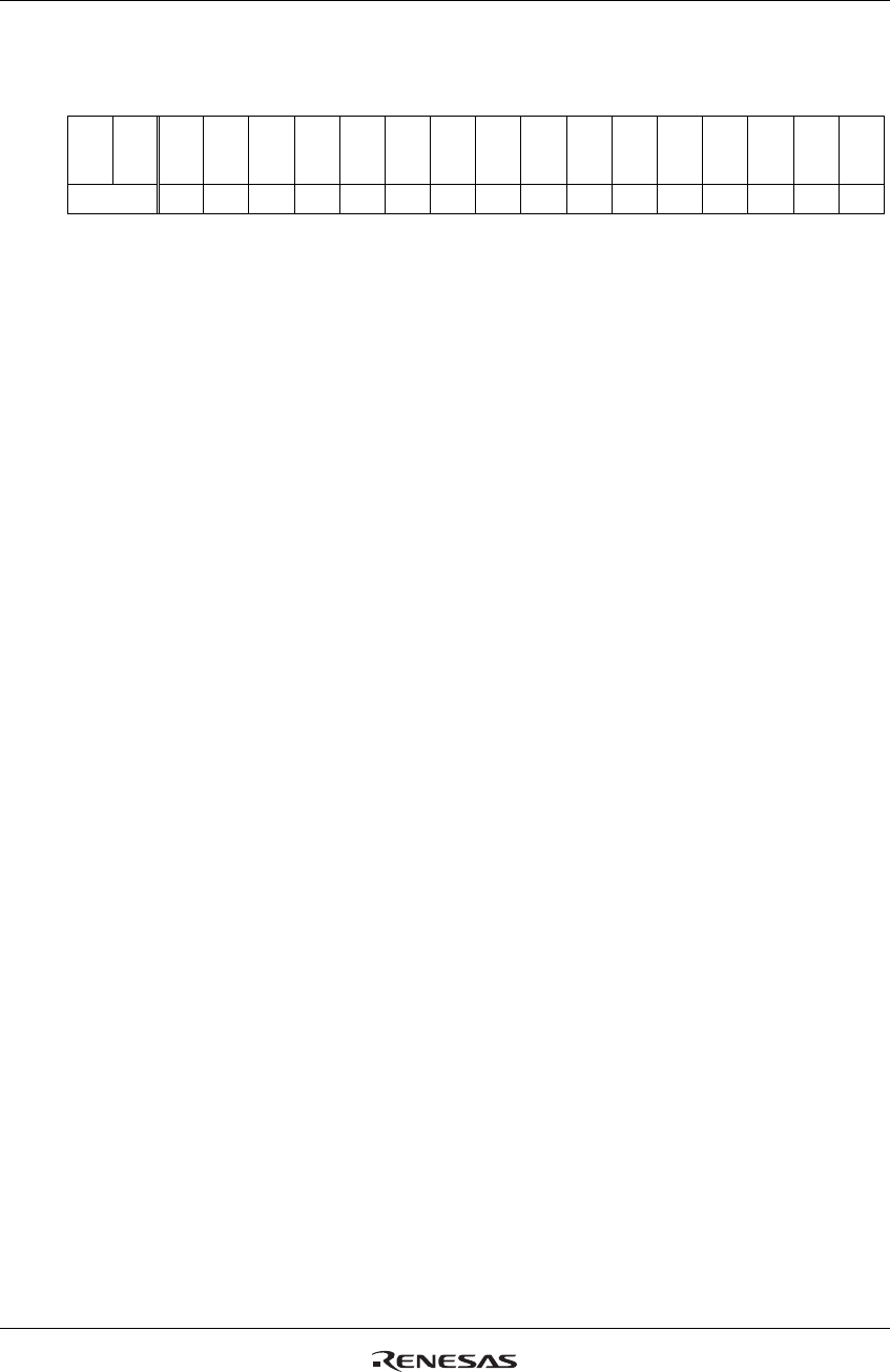
R61509V Target Spec
Rev. 0.11 April 25, 2008, page 78 of 181
NVM Data Read / NVM Data Write (R280h)
UID[3:0]: Used to temporarily store NVM data such as used identification code.
The write data is loaded to NVM data write register (NVDAT [7:0]) and then is written to NVM.
NVM data is loaded to UID[7:0] when power on reset, when shutdown mode is exited or when CALB=1 is
written. When NVM data write is not executed, UID[7:0] = 8’hFF (Default).
VCM[6:0]: Used to control VCOMH.
To use NVM data to adjust VCOMH, specify the VCOMH level using VCM [6:0], write the same value to
the NVM data write register NVDAT [14:8] (R6F1h) and then write the data to NVM.
NVM data is loaded to VCM[6:0] when power on reset, when shutdown mode is exited or when CALB=1
is written. When NVM data write is not executed, VCM[6:0]= 7’h7F (Default).
R/W RS IB15 IB14 IB13 IB12 IB11 IB10 IB9 IB8 IB7 IB6 IB5 IB4 IB3 IB2 IB1 IB0
R
280h R/W 1 1
VC
M
[6]
VC
M
[5]
VC
M
[4]
VC
M
[3]
VC
M
[2]
VC
M
[1]
VC
M
[0]
UID
[7]
UID
[6]
UID
[5]
UID
[4]
UID
[3]
UID
[2]
UID
[1]
UID
[0]
Default 1 1 1 1 1 1 1 1 1 1 1 1 1 1 1 1
R61509V Target Spec
Rev. 0.11 April 25, 2008, page 79 of 181
Table 48
VCM [6:0] VCOMH voltage VCM [6:0] VCOMH voltage
7’h00 VREG1OUT x 0.492 7’h40 VREG1OUT x 0.748
7’h01 VREG1OUT x 0.496 7’h41 VREG1OUT x 0.752
7’h02 VREG1OUT x 0.500 7’h42 VREG1OUT x 0.756
7’h03 VREG1OUT x 0.504 7’h43 VREG1OUT x 0.760
7’h04 VREG1OUT x 0.508 7’h44 VREG1OUT x 0.764
7’h05 VREG1OUT x 0.512 7’h45 VREG1OUT x 0.768
7’h06 VREG1OUT x 0.516 7’h46 VREG1OUT x 0.772
7’h07 VREG1OUT x 0.520 7’h47 VREG1OUT x 0.776
7’h08 VREG1OUT x 0.524 7’h48 VREG1OUT x 0.780
7’h09 VREG1OUT x 0.528 7’h49 VREG1OUT x 0.784
7’h0A VREG1OUT x 0.532 7’h4A VREG1OUT x 0.788
7’h0B VREG1OUT x 0.536 7’h4B VREG1OUT x 0.792
7’h0C VREG1OUT x 0.540 7’h4C VREG1OUT x 0.796
7’h0D VREG1OUT x 0.544 7’h4D VREG1OUT x 0.800
7’h0E VREG1OUT x 0.548 7’h4E VREG1OUT x 0.804
7’h0F VREG1OUT x 0.552 7’h4F VREG1OUT x 0.808
7’h10 VREG1OUT x 0.556 7’h50 VREG1OUT x 0.812
7’h11 VREG1OUT x 0.560 7’h51 VREG1OUT x 0.816
7’h12 VREG1OUT x 0.564 7’h52 VREG1OUT x 0.820
7’h13 VREG1OUT x 0.568 7’h53 VREG1OUT x 0.824
7’h14 VREG1OUT x 0.572 7’h54 VREG1OUT x 0.828
7’h15 VREG1OUT x 0.576 7’h55 VREG1OUT x 0.832
7’h16 VREG1OUT x 0.580 7’h56 VREG1OUT x 0.836
7’h17 VREG1OUT x 0.584 7’h57 VREG1OUT x 0.840
7’h18 VREG1OUT x 0.588 7’h58 VREG1OUT x 0.844
7’h19 VREG1OUT x 0.592 7’h59 VREG1OUT x 0.848
7’h1A VREG1OUT x 0.596 7’h5A VREG1OUT x 0.852
7’h1B VREG1OUT x 0.600 7’h5B VREG1OUT x 0.856
7’h1C VREG1OUT x 0.604 7’h5C VREG1OUT x 0.860
7’h1D VREG1OUT x 0.608 7’h5D VREG1OUT x 0.864
7’h1E VREG1OUT x 0.612 7’h5E VREG1OUT x 0.868
7’h1F VREG1OUT x 0.616 7’h5F VREG1OUT x 0.872
7’h20 VREG1OUT x 0.620 7’h60 VREG1OUT x 0.876
7’h21 VREG1OUT x 0.624 7’h61 VREG1OUT x 0.880
7’h22 VREG1OUT x 0.628 7’h62 VREG1OUT x 0.884
7’h23 VREG1OUT x 0.632 7’h63 VREG1OUT x 0.888
7’h24 VREG1OUT x 0.636 7’h64 VREG1OUT x 0.892
7’h25 VREG1OUT x 0.640 7’h65 VREG1OUT x 0.896
7’h26 VREG1OUT x 0.644 7’h66 VREG1OUT x 0.900
7’h27 VREG1OUT x 0.648 7’h67 VREG1OUT x 0.904
7’h28 VREG1OUT x 0.652 7’h68 VREG1OUT x 0.908
7’h29 VREG1OUT x 0.656 7’h69 VREG1OUT x 0.912
7’h2A VREG1OUT x 0.660 7’h6A VREG1OUT x 0.916
7’h2B VREG1OUT x 0.664 7’h6B VREG1OUT x 0.920
7’h2C VREG1OUT x 0.668 7’h6C VREG1OUT x 0.924
7’h2D VREG1OUT x 0.672 7’h6D VREG1OUT x 0.928
7’h2E VREG1OUT x 0.676 7’h6E VREG1OUT x 0.932
7’h2F VREG1OUT x 0.680 7’h6F VREG1OUT x 0.936
7’h30 VREG1OUT x 0.684 7’h70 VREG1OUT x 0.940
7’h31 VREG1OUT x 0.688 7’h71 VREG1OUT x 0.944
7’h32 VREG1OUT x 0.692 7’h72 VREG1OUT x 0.948
7’h33 VREG1OUT x 0.696 7’h73 VREG1OUT x 0.952
7’h34 VREG1OUT x 0.700 7’h74 VREG1OUT x 0.956
7’h35 VREG1OUT x 0.704 7’h75 VREG1OUT x 0.960
7’h36 VREG1OUT x 0.708 7’h76 VREG1OUT x 0.964
7’h37 VREG1OUT x 0.712 7’h77 VREG1OUT x 0.968
R61509V Target Spec
Rev. 0.11 April 25, 2008, page 80 of 181
7’h38 VREG1OUT x 0.716 7’h78 VREG1OUT x 0.972
7’h39 VREG1OUT x 0.720 7’h79 VREG1OUT x 0.976
7’h3A VREG1OUT x 0.724 7’h7A VREG1OUT x 0.980
7’h3B VREG1OUT x 0.728 7’h7B VREG1OUT x 0.984
7’h3C VREG1OUT x 0.732 7’h7C VREG1OUT x 0.988
7’h3D VREG1OUT x 0.736 7’h7D VREG1OUT x 0.992
7’h3E VREG1OUT x 0.740 7’h7E VREG1OUT x 0.996
7’h3F VREG1OUT x 0.744 7’h7F VREG1OUT x 1.000
Notes: 1. Make sure the VCOMH level is between 3.0V to (DDVDH-0.5)V.
2. The above setting is enabled when internal electronic volume is selected for setting the VCOMH
level.
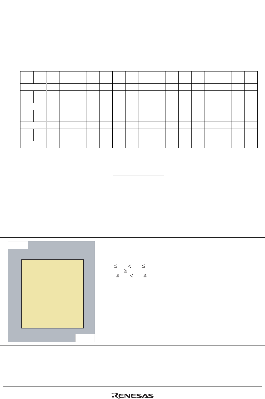
R61509V Target Spec
Rev. 0.11 April 25, 2008, page 81 of 181
Window Address Control
Window Horizontal RAM Address Start (R210h), Window Horizontal RAM Address End
(R211h)
Window Vertical RAM Address Start (R212h), Window Vertical RAM Address End (R213h)
HSA[7:0], HEA[7:0]: HSA[7:0] and HEA[7:0] specify the start and end addresses of the window address
area in horizontal direction, respectively. See GRAM Address Map. HSA[7:0] and HEA[7:0] specify the
horizontal range to write data. Set HSA[7:0] and HEA[7:0] before starting RAM write operation. In
setting, make sure that 8’h00 ≤ HSA < HEA ≤ 8’hEF.
VSA[8:0], VEA[8:0]: VSA[8:0] and VEA[8:0] specify the start and end addresses of the window address
area in vertical direction, respectively. See GRAM Address Map. VSA[8:0] and VEA[8:0] specify the
vertical range to write data. Set VSA[8:0] and VEA[8:0] before starting RAM write operation. In setting,
make sure that 9’h000 ≤ VSA < VEA ≤ 9’h1AF.
17'h000-00
17'h1AF-EF
Notes: 1. Make an window address area within the GRAM address area.
2. Set an address within the window address area.
Window address area
Window address area setting range:
8'h00 HSA HEA 8'hEF,
HEA - HSA 8'h4,
9'h000 VSA VEA 9'h1AF
HEA
HSA
VSA
VEA
Figure 9 GRAM Address Map and Window Address Area
R/W RS IB15 IB14 IB13 IB12 IB11 IB10 IB9 IB8 IB7 IB6 IB5 IB4 IB3 IB2 IB1 IB0
R
210 R/W 1 0 0 0 0 0 0 0 0
HSA
[7]
HSA
[6]
HSA
[5]
HSA
[4]
HSA
[3]
HSA
[2]
HSA
[1]
HSA
[0]
Default 0 0 0 0 0 0 0 0 0 0 0 0 0 0 0 0
R
211 R/W 1 0 0 0 0 0 0 0 0
HEA
[7]
HEA
[6]
HEA
[5]
HEA
[4]
HEA
[3]
HEA
[2]
HEA
[1]
HEA
[0]
Default 0 0 0 0 0 0 0 0 1 1 1 0 1 1 1 1
R
212 R/W 1 0 0 0 0 0 0 0
VSA
[8]
VSA
[7]
VSA
[6]
VSA
[5]
VSA
[4]
VSA
[3]
VSA
[2]
VSA
[1]
VSA
[0]
Default 0 0 0 0 0 0 0 0 0 0 0 0 0 0 0 0
R
213 R/W 1 0 0 0 0 0 0 0
VEA
[8]
VEA
[7]
VEA
[6]
VEA
[5]
VEA
[4]
VEA
[3]
VEA
[2]
VEA
[1]
VEA
[0]
Default 0 0 0 0 0 0 0 1 1 0 1 0 1 1 1 1
R61509V Target Spec
Rev. 0.11 April 25, 2008, page 82 of 181
γ Control
γ Control 1 ~ 14 (R300h to R309h)
R/W RS IB15 IB14 IB13 IB12 IB11 IB10 IB9 IB8 IB7
IB
6 IB5 IB4 IB3 IB2 IB1 IB0
R
300 W 1 0 0 0
PR0
P01
[4]
PR0
P01
[3]
PR0
P01
[2]
PR0
P01
[1]
PR0
P01
[0]
0 0 0
PR0P
00[4]
PR0P
00[3]
PR0P
00[2]
PR0
P00
[1]
PR0
P00
[0]
Default 0 0 0 0 0 0 0 0 0 0 0 0 0 0 0 0
R
301 W 1
PR0
P04
[3]
PR0
P04
[2]
PR0
P04
[1]
PR0
P04
[0]
PR0
P03
[3]
PR0
P03
[2]
PR0
P03
[1]
PR0
P03
[0]
0 0 0
PR0P
02[4]
PR0P
02[3]
PR0P
02[2]
PR0
P02
[1]
PR0
P02
[0]
Default 0 0 0 0 0 0 0 0 0 0 0 0 0 0 0 0
R
302 W 1 0 0 0
PR0
P06
[4]
PR0
P06
[3]
PR0
P06
[2]
PR0
P06
[1]
PR0
P06
[0]
0 0 0 0
PR0P
05[3]
PR0P
05[2]
PR0
P05
[1]
PR0
P05
[0]
Default 0 0 0 0 0 0 0 0 0 0 0 0 0 0 0 0
R
303 W 1 0 0 0
PR0
P08
[4]
PR0
P08
[3]
PR0
P08
[2]
PR0
P08
[1]
PR0
P08
[0]
0 0 0
PR0P
07[4]
PR0P
07[3]
PR0P
07[2]
PR0
P07
[1]
PR0
P07
[0]
Default 0 0 0 0 0 0 0 0 0 0 0 0 0 0 0 0
R
304 W 1 0 0
PI0
P3
[1]
PI0
P3
[0]
0 0
PI0
P2
[1]
PI0
P2
[0]
0 0
PI0
P1
[1]
PI0
P1
[0]
0 0
PI0
P0
[1]
PI0
P0
[0]
Default 0 0 0 0 0 0 0 0 0 0 0 0 0 0 0 0
R
305 W 1 0 0 0
PR0
N01
[4]
PR0
N01
[3]
PR0
N01
[2]
PR0
N01
[1]
PR0
N01
[0]
0 0 0
PR0
N00
[4]
PR0
N00
[3]
PR0
N00
[2]
PR0
N00
[1]
PR0
N00
[0]
Default 0 0 0 0 0 0 0 0 0 0 0 0 0 0 0 0
R
306 W 1
PR0
N04
[3]
PR0
N04
[2]
PR0
N04
[1]
PR0
N04
[0]
PR0
N03
[3]
PR0
N03
[2]
PR0
N03
[1]
PR0
N03
[0]
0 0 0
PR0
N02
[4]
PR0
N02
[3]
PR0
N02
[2]
PR0
N02
[1]
PR0
N02
[0]
Default 0 0 0 0 0 0 0 0 0 0 0 0 0 0 0 0
R
307 W 1 0 0 0
PR0
N06
[4]
PR0
N06
[3]
PR0
N06
[2]
PR0
N06
[1]
PR0
N06
[0]
0 0 0 0
PR0
N05
[3]
PR0
N05
[2]
PR0
N05
[1]
PR0
N05
[0]
Default 0 0 0 0 0 0 0 0 0 0 0 0 0 0 0 0
R
308 W 1 0 0 0
PR0
N08
[4]
PR0
N08
[3]
PR0
N08
[2]
PR0
N08
[1]
PR0
N08
[0]
0 0 0
PR0
N07
[4]
PR0
N07
[3]
PR0
N07
[2]
PR0
N07
[1]
PR0
N07
[0]
Default 0 0 0 0 0 0 0 0 0 0 0 0 0 0 0 0
R
309 W 1 0 0
PI0
N3
[1]
PI0
N3
[0]
0 0
PI0
N2
[1]
PI0
N2
[0]
0 0
PI0
N1
[1]
PI0
N 1
[0]
0 0
PI0
N0
[1]
PI0
N0
[0]
Default 0 0 0 0 0 0 0 0 0 0 0 0 0 0 0 0

R61509V Target Spec
Rev. 0.11 April 25, 2008, page 83 of 181
PR0P00[4:0]
PR0N00[4:0]
Adjusts reference level for positive polarity output R0
Adjusts reference level for negative polarity output R0
PR0P01[4:0]
PR0N01[4:0]
Adjusts reference level for positive polarity output R1
Adjusts reference level for negative polarity output R1
PR0P02[4:0]
PR0N02[4:0]
Adjusts reference level for positive polarity output R2
Adjusts reference level for negative polarity output R2
PR0P03[3:0]
PR0N03[3:0]
Adjusts reference level for positive polarity output R3
Adjusts reference level for negative polarity output R3
PR0P04[3:0]
PR0N04[3:0]
Adjusts reference level for positive polarity output R4
Adjusts reference level for negative polarity output R4
PR0P05[3:0]
PR0N05[3:0]
Adjusts reference level for positive polarity output R5
Adjusts reference level for negative polarity output R5
PR0P06[4:0]
PR0N06[4:0]
Adjusts reference level for positive polarity output R6
Adjusts reference level for negative polarity output R6
PR0P07[4:0]
PR0N07[4:0]
Adjusts reference level for positive polarity output R7
Adjusts reference level for negative polarity output R7
PR0P08[4:0]
PR0N08[4:0]
Adjusts reference level for positive polarity output R8
Adjusts reference level for negative polarity output R8
PI0P0~1[1:0]
PI0N0~1[1:0]
Adjusts interpolation level for positive polarity output (V2~V7)
Adjusts interpolation level for negative polarity output (V2~V7)
PI0P2~3[1:0]
PI0N2~3[1:0]
Adjusts interpolation level for positive polarity output (V56~V61)
Adjusts interpolation level for negative polarity output (V56~V61)
R61509V Target Spec
Rev. 0.11 April 25, 2008, page 84 of 181
Base Image Display Control
Base Image Number of Line (R400h)
Base Image Display Control (R401h)
Base Image Vertical Scroll Control (R404h)
GS: Sets the direction of scan by the gate driver in the range determined by SCN and NL bits. The gate
scan direction determined by setting GS = 0 is reversed by setting GS = 1. Set GS bit in combination with
SM bits.
NL[5:0]: Sets the number of lines to drive the LCD at an interval of 8 lines. The GRAM address mapping
is not affected by the number of lines set by NL[5:0]. The number of lines must be the same or more than
the number of lines necessary for the size of the liquid crystal panel.
SCN[5:0]: Specifies the gate line where the gate driver starts scan.
NDL: Sets the source output level in non-lit display area. Settings are different depending on panel type
(i.e. normally black or normally white).
Table 49
Non-lit display area NDL
Positive Negative
0 V63 V0
1 V0 V63
Note: NDL setting is enabled in non-lit display area in partial display operation.
VLE: Vertical scroll display enable bit. When VLE = 1, the R61509V starts displaying the base image
from the line (of the physical display) determined by VL[8:0] bits. VL[8:0] sets the amount of scrolling,
which is the number of lines to shift the start line of the display from the first line of the physical display.
Note that the partial image display position is not affected by the base image scrolling.
The vertical scrolling is disabled in external display interface operation. In this case, make sure to set VLE
= “0”.
R/W RS IB15 IB14 IB13 IB12 IB11 IB10 IB9 IB8 IB7 IB6 IB5 IB4 IB3 IB2 IB1 IB0
R
400 R/W 1 GS NL
[5]
NL
[4]
NL
[3]
NL
[2]
NL
[1]
NL
[0] 0 0
SCN
[5]
SCN
[4]
SCN
[3]
SCN
[2]
SCN
[1]
SCN
[0] 0
Default 0 1 1 0 1 0 1 0 0 0 0 0 0 0 0 0
R
401 R/W 1 0 0 0 0 0 0 0 0 0 0 0 0 0 NDL VLE REV
Default 0 0 0 0 0 0 0 0 0 0 0 0 0 0 0 0
R
404 R/W 1 0 0 0 0 0 0 0
VL
[8]
VL
[7]
VL
[6]
VL
[5]
VL
[4]
VL
[3]
VL
[2]
VL
[1]
VL
[0]
Default 0 0 0 0 0 0 0 0 0 0 0 0 0 0 0 0
R61509V Target Spec
Rev. 0.11 April 25, 2008, page 85 of 181
Table 50
VLE Base image
0 Fixed
1 Scrolling enabled
REV: Grayscale level of a image is inverted when REV = 1. This enables the R61509V to display the
same image from the same set of data both on normally black and white panels.
Table 51
Source Output Level in Display Area
REV GRAM Data Positive Polarity Negative Polarity
18’h00000 V63 V0
: : :
0
18’h3FFFFF V0 V63
18’h00000 V0 V63
: : :
1
18’h3FFFFF V63 V0
Note: Source output of non-lit display area is set by NDL bit during partial display mode.
VL[8:0]: Sets the amount of scrolling of the base image. The base image is scrolled in vertical direction
and displayed from the line which is determined by VL.
Table 52
VL [8:0] Line per scrolling
9’h000 0 lines
9’h001 1 line
9’h002 2 lines
:
:
:
:
9’h1A0 431 lines
9’h1B0 432 lines
9’h1FF Setting inhibited
R61509V Target Spec
Rev. 0.11 April 25, 2008, page 86 of 181
Table 53
NL [5:0] Number of drive line NL [5:0] Number of drive line
6’h00 Setting inhibited
6’h1C 232 lines
6’h01 16 lines 6’h1D 240 lines
6’h02 24 lines 6’h1E 248 lines
6’h03 32 lines 6’h1F 256 lines
6’h04 40 lines 6’h20 264 lines
6’h05 48 lines 6’h21 272 lines
6’h06 56 lines 6’h22 280 lines
6’h07 64 lines 6’h23 288 lines
6’h08 72 lines 6’h24 296 lines
6’h09 80 lines 6’h25 304 lines
6’h0A 88 lines 6’h26 312 lines
6’h0B 96 lines 6’h27 320 lines
6’h0C 104 lines 6'h28 328 lines
6’h0D 112 lines 6'h29 336 lines
6’h0E 120 lines 6'h2A 344 lines
6’h0F 128 lines 6'h2B 352 lines
6’h10 136 lines 6'h2C 360 lines
6’h11 144 lines 6'h2D 368 lines
6’h12 152 lines 6'h2E 376 lines
6’h13 160 lines 6'h2F 384 lines
6’h14 168 lines 6'h30 392 lines
6’h15 176 lines 6'h31 400 lines
6’h16 184 lines 6'h32 408 lines
6’h17 192 lines 6'h33 416 lines
6’h18 200 lines 6'h34 424 lines
6’h19 208 lines 6'h35 432 lines
6’h1A 216 lines 6'h36-6'h3F Setting inhibited
6’h1B 224 lines
R61509V Target Spec
Rev. 0.11 April 25, 2008, page 87 of 181
Table 54
Gate scan start position
SM=0 SM=1
SCN[5:0]
GS=0 GS=1 GS=0 GS=1
6’h00 G1 G(N) G1 G(2N-432)
6’h01 G9 G(N+8) G17 G(2N-416)
6’h02 G17 G(N+16) G33 G(2N-400)
6’h03 G25 G(N+24) G49 G(2N-384)
6’h04 G33 G(N+32) G65 G(2N-368)
6’h05 G41 G(N+40) G81 G(2N-352)
6’h06 G49 G(N+49) G97 G(2N-336)
6’h07 G57 G(N+56) G113 G(2N-320)
6’h08 G65 G(N+64) G129 G(2N-304)
6’h09 G73 G(N+72) G145 G(2N-288)
6’h0A G81 G(N+80) G161 G(2N-272)
6’h0B G89 G(N+88) G177 G(2N-256)
6’h0C G97 G(N+96) G193 G(2N-240)
6’h0D G105 G(N+104) G209 G(2N-224)
6’h0E G113 G(N+112) G225 G(2N-208)
6’h0F G121 G(N+120) G241 G(2N-192)
6’h10 G129 G(N+128) G257 G(2N-176)
6’h11 G137 G(N+136) G273 G(2N-160)
6’h12 G145 G(N+144) G289 G(2N-144)
6’h13 G153 G(N+152) G305 G(2N-128)
6’h14 G161 G(N+160) G321 G(2N-112)
6’h15 G169 G(N+168) G337 G(2N-96)
6’h16 G177 G(N+176) G353 G(2N-80)
6’h17 G185 G(N+184) G369 G(2N-64)
6’h18 G193 G(N+192) G385 G(2N-48)
6’h19 G201 G(N+200) G401 G(2N-32)
6’h1A G209 G(N+208) G417 G(2N-16)
6’h1B G217 G(N+216) G2 G(2N-431)
6’h1C G225 G(N+224) G18 G(2N-415)
6’h1D G233 G(N+232) G34 G(2N-399)
6’h1E G241 G(N+240) G50 G(2N-383)
6’h1F G249 G(N+248) G66 G(2N-367)
6’h20 G257 G(N+256) G82 G(2N-351)
6’h21 G265 G(N+264) G98 G(2N-335)
6’h22 G273 G(N+272) G114 G(2N-319)
6’h23 G281 G(N+280) G130 G(2N-303)
6’h24 G289 G(N+288) G146 G(2N-287)
6’h25 G297 G(N+296) G162 G(2N-271)
6’h26 G305 G(N+304) G178 G(2N-255)
6’h27 G313 G(N+312) G194 G(2N-239)
6’h28 G321 G(N+320) G210 G(2N-223)
6’h29 G329 G(N+328) G226 G(2N-207)
6’h2A G337 G(N+337) G242 G(2N-191)
6’h2B G345 G(N+344) G258 G(2N-175)
6’h2C G353 G(N+352) G274 G(2N-159)
6’h2D G361 G(N+360) G290 G(2N-143)
6’h2E G369 G(N+368) G306 G(2N-127)
6’h2F G377 G(N+376) G322 G(2N-111)
6’h30 G385 G(N+384) G338 G(2N-95)
6’h31 G393 G(N+392) G354 G(2N-79)
6’h32 G401 G(N+400) G370 G(2N-63)
6’h33 G409 G(N+408) G386 G(2N-47)
6’h34 G417 G(N+416) G402 G(2N-31)
6’h35-6’h3F Setting inhibited Setting inhibited Setting inhibited Setting inhibited
Note: “N” is the number of line decided by NL [5:0] bit.
Make sure that (Gate scan start position + NL = Gate scan end position) does not exceed 432 lines.
R61509V Target Spec
Rev. 0.11 April 25, 2008, page 88 of 181
Partial Display Control
Partial Image 1: Display Position (R500h), RAM Address 1 (Start Line Address) (R501h), RAM
Address 1 (End Line Address) (R502h)
PTDP[8:0]: Sets the display position of partial image 1.
If PTDP0 = “9’h000”, the partial image 1 is displayed from the first line of the base image.
PTSA[8:0] and PTEA[8:0]: Sets the start line and end line addresses of the RAM area, respectively for the
partial image 1. In setting, make sure that PTSA ≤ PTEA.
R/W RS IB15 IB14 IB13 IB12 IB11 IB10 IB9 IB8 IB7 IB6 IB5 IB4 IB3 IB2 IB1 IB0
R
500h
R/W 1 0 0 0 0 0 0 0
PTD
P [8]
PTD
P [7]
PTD
P [6]
PTD
P [5]
PTD
P [4]
PTD
P [3]
PTD
P [2]
PTD
P [1]
PTD
P [0]
Default 0 0 0 0 0 0 0 0 0 0 0 0 0 0 0 0
R
501h
R/W 1 0 0 0 0 0 0 0
PTS
A [8]
PTS
A [7]
PTS
A [6]
PTS
A [5]
PTS
A [4]
PTS
A [3]
PTS
A [2]
PTS
A [1]
PTS
A [0]
Default 0 0 0 0 0 0 0 0 0 0 0 0 0 0 0 0
R
502h
R/W 1 0 0 0 0 0 0 0
PTE
A
[8]
PTE
A
0[7]
PTE
A [6]
PTE
A [5]
PTE
A [4]
PTE
A [3]
PTE
A [2]
PTE
A [1]
PTE
A [0]
Default 0 0 0 0 0 0 0 0 0 0 0 0 0 0 0 0
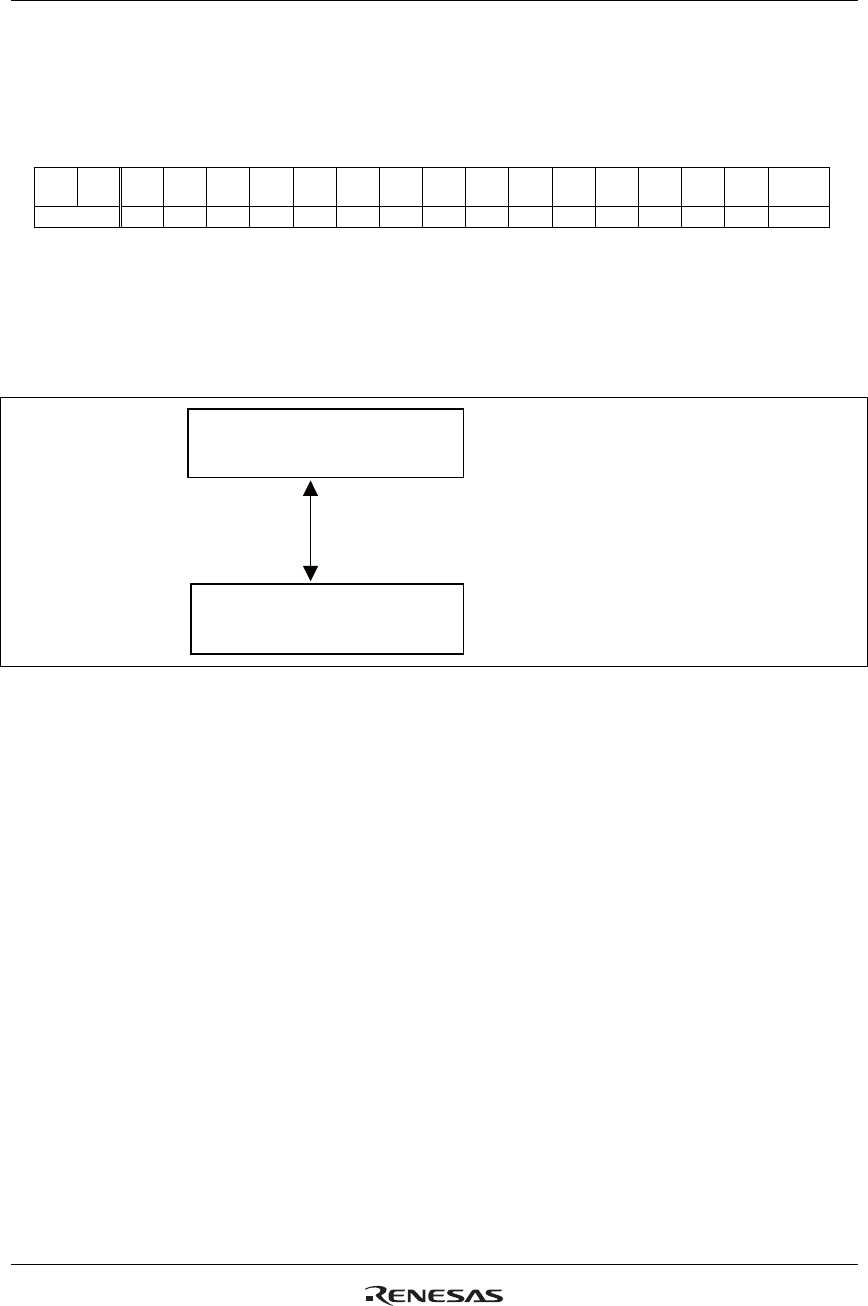
R61509V Target Spec
Rev. 0.11 April 25, 2008, page 89 of 181
Pin Control
Test Register (Software Reset) (R600h)
TRSR: When TRSR = 1, test registers are initialized.
When TRSR = 0, initialization of test registers halts.
Instruction Write
R600h TRSR="1"
R600h TRSR="0"㩷
Instruction Write
Test registers are initialized (0.1ms or longer)
Figure 10
R/W RS IB15 IB14 IB13 IB12 IB11 IB10 IB9 IB8 IB7 IB6 IB5 IB4 IB3 IB2 IB1 IB0
R/W 1 0 0 0 0 0 0 0 0 0 0 0 0 0 0 0 TRSR
Default value 0 0 0 0 0 0 0 0 0 0 0 0 0 0 0 0
R61509V Target Spec
Rev. 0.11 April 25, 2008, page 90 of 181
NVM Control
NVM Access Control 1 (R6F0h), NVM Access Control 2 (R6F1h), NVM Access Control 3
(R6F2h)
EOP [1:0]: Writes data on R280h to NVM or halts the write operation.
Table 55
EOP[1:0] NVM control
2’h0 Halt
2’h1 Write
2’h2 Setting disabled
2’h3 Erase
CALB: When CALB=1, all data in NVM is read out and written to internal registers. When finished,
CALB is set to 0.
TE: Enables internal NVM control bit (EOP). Follow the NVM control sequence when setting TE.
NVDAT[15:0]: To write data to NVM, write the data on NVDAT (R6F1h) first, and then start write
operation using EOP bit.
・ NVM data written to NVDAT[14:8] are loaded to R280h VCM [6:0] when power on reset is executed
or CALB=1.
・ NVM data written to NVDAT[7:0] are loaded to R280h UID [7:0] when power on reset is executed or
CALB=1.
See “NVM Control” for details of write operation and required settings.
R/W RS IB15 IB14 IB13 IB12 IB11 IB10 IB9 IB8 IB7 IB6 IB5 IB4 IB3 IB2 IB1 IB0
R
6F0h R/W 1 0 0 0 0 0 0 0 0 TE CAL
B
EOP
[1]
EOP
[0] 0 0 0 0
Default 0 0 0 0 0 0 0 0 0 0 0 0 0 0 0 0
R
6F1h R/W 1
NV
DAT
[15]
NV
DAT
[14]
NV
DAT
[13]
NV
DAT
[12]
NV
DAT
[11]
NV
DAT
[10]
NV
DAT
[9]
NV
DAT
[8]
NV
DAT
[7]
NV
DAT
[6]
NV
DAT
[5]
NV
DAT
[4]]
NV
DAT
[3]
NV
DAT
[2]]
NV
DAT
[1]
NV
DAT
[0]
Default 0 0 0 0 0 0 0 0 0 0 0 0 0 0 0 0
R/W 1 0 0 0 0 0 0 0 0 0 0 0 0
NVV
RF 0 0 0
R
6F2h
Default 0 0 0 0 0 0 0 0 0 0 0 0 0 0 0 0
R61509V Target Spec
Rev. 0.11 April 25, 2008, page 91 of 181
R6F1h
Write data to NVM
(NVM)
Read data from NVM
R280h
Write “1” to NVDAT[15].
㪥㪭㩷
㪛㪘㪫㩷
㪲㪈㪌㪴㩷
㪥㪭㩷
㪛㪘㪫㩷
㪲㪈㪋㪴㩷
㪥㪭㩷
㪛㪘㪫㩷
㪲㪈㪊㪴㩷
㪥㪭㩷
㪛㪘㪫㩷
㪲㪈㪉㪴㩷
㪥㪭
㪛㪘㪫
㪲㪈㪈㪴
㪥㪭
㪛㪘㪫
㪲㪈㪇㪴
㪥㪭
㪛㪘㪫
㪲㪐㪴
㪥㪭
㪛㪘㪫
㪲㪏㪴
㪥㪭
㪛㪘㪫
㪲㪎㪴
㪥㪭
㪛㪘㪫
㪲㪍㪴
㪥㪭
㪛㪘㪫
㪲㪌㪴
㪥㪭
㪛㪘㪫
㪲㪋㪴
㪥㪭㩷
㪛㪘㪫㩷
㪲㪊㪴㩷
㪥㪭㩷
㪛㪘㪫㩷
㪲㪉㪴㩷
㪥㪭㩷
㪛㪘㪫㩷
㪲㪈㪴㩷
㪥㪭
㪛㪘㪫
㪲㪇㪴
㸣㩷㸣㩷㸣㩷㸣㩷㸣 㸣 㸣 㸣 㸣 㸣 㸣 㸣 㸣㩷㸣㩷㸣㩷㸣
㪥㪭㪤㩷
㪲㪈㪌㪴㩷
㪥㪭㪤㩷
㪲㪈㪋㪴㩷
㪥㪭㪤㩷
㪲㪈㪊㪴㩷
㪥㪭㪤㩷
㪲㪈㪉㪴㩷
㪥㪭㪤
㪲㪈㪈㪴
㪥㪭㪤
㪲㪈㪇㪴
㪥㪭㪤
㪲㪐㪴
㪥㪭㪤
㪲㪏㪴
㪥㪭㪤
㪲㪎㪴
㪥㪭㪤
㪲㪍㪴
㪥㪭㪤
㪲㪌㪴
㪥㪭㪤
㪲㪋㪴
㪥㪭㪤㩷
㪲㪊㪴㩷
㪥㪭㪤㩷
㪲㪉㪴㩷
㪥㪭㪤㩷
㪲㪈㪴㩷
㪥㪭㪤
㪲㪇㪴
㸣㩷㸣㩷㸣㩷㸣㩷㸣㸣㸣㸣㸣㸣㸣㸣㸣㩷㸣㩷㸣㩷㸣
㪈㩷
㪭㪚㪤㩷
㪲㪍㪴㩷
㪭㪚㪤㩷
㪲㪌㪴㩷
㪭㪚㪤㩷
㪲㪋㪴㩷
㪭㪚㪤
㪲㪊㪴
㪭㪚㪤
㪲㪉㪴
㪭㪚㪤
㪲㪈㪴
㪭㪚㪤
㪲㪇㪴
㪬㪠㪛
㪲㪎㪴
㪬㪠㪛
㪲㪍㪴
㪬㪠㪛
㪲㪌㪴
㪬㪠㪛
㪲㪋㪴
㪬㪠㪛㩷
㪲㪊㪴㩷
㪬㪠㪛㩷
㪲㪉㪴㩷
㪬㪠㪛㩷
㪲㪈㪴㩷
㪬㪠㪛
㪲㪇㪴
Figure 11
NVVRF: Enables erase verify. This bit is used only in the NVM erase sequence. See “NVM Erase
Sequence” for details.
●R61509V Instruction List Rev 0.50 2008. 04. 22
Middle category
Upper Index Index Command IB15 IB14 IB13 IB12 IB11 IB10 IB9 IB8 IB7 IB6 IB5 IB4 IB3 IB2 IB1 IB0
- Index - Index 00000ID10 ID9 ID8 ID7 ID6 ID5 ID4 ID3 ID2 ID21 ID0
0** Display Control 00* 000h Device Code Read ALMID1[7]
(1)
ALMID1[6]
(0)
ALMID1[5]
(1)
ALMID1[4]
(1)
ALMID1[3]
(0)
ALMID1[2]
(1)
ALMID1[1]
(0)
ALMID1[0]
(1)
ALMID0[7]
(0)
ALMID0[6]
(0)
ALMID0[5]
(0)
ALMID0[4]
(0)
ALMID0[3]
(1)
ALMID0[2]
(0)
ALMID0[1]
(0)
ALMID0[0]
(1)
Display Control
in general 001h Driver Output Control 00000
SM
(0) 0SS
(0) 00000000
002h LCD Drive Waveform Control 0000000
BC
(0) 00000000
003h Entry Mode TRI
(0)
DFM
(0) 0BGR
(0) 0000
ORG
(0) 0ID[1]
(1)
ID[0]
(1)
AM
(0) 000
004h Setting inhibited 0000000000000000
005h Setting inhibited 0000000000000000
006h Setting inhibited 0000000000000000
007h Display Control 1 000
PTDE
(0) 000
BASEE
(0) 00000000
008h Display Control 2 FP[7]
(0)
FP[6]
(0)
FP[5]
(0)
FP[4]
(0)
FP[3]
(1)
FP[2]
(0)
FP[1]
(0)
FP[0]
(0)
BP[7]
(0)
BP[6]
(0)
BP[5]
(0)
BP[4]
(0)
BP[3]
(1)
BP[2]
(0)
BP[1]
(0)
BP[0]
(0)
009h Display Control 3 0000
PTV
(0)
PTS
(0) 0000000000
00Ah Setting inhibited 0000000000000000
00Bh 8 Color Control 000000000011000
COL
(0)
00Ch External Display Interface Control
10ENC[2]
(0)
ENC[1]
(0)
ENC[0]
(0) 000
RM
(0) 00
DM[1]
(0)
DM[0]
(0) 000
RIM
(0)
00D-00Eh Setting inhibited 0000000000000000
00Fh External Display Interface Control
200000000000
VSPL
(0)
HSPL
(0) 0EPL
(0)
DPL
(0)
01* 010h Panel Interface Control 1 000000
DIVI[1]
(0)
DIVI[0]
(0) 000
RTNI[4]
(1)
RTNI[3]
(1)
RTNI[2]
(0)
RTNI[1]
(0)
RTNI[0]
(1)
Panel Interface
(Internal Clock) 011h Panel Interface Control 2 00000
NOWI[2]
(0)
NOWI[1]
(0)
NOWI[0]
(1) 00000
SDTI[2]
(0)
SDTI[1]
(0)
SDTI[0]
(1)
012h Panel Interface Control 3 00000
VEQWI[2]
(0)
VEQWI[1]
(0)
VEQWI[0]
(0) 00000
SEQWI[2]
(0)
SEQWI[1]
(0)
SEQWI[0]
(0)
013h Panel Interface Control 4 0000000000000
MCPI[2]
(0)
MCPI[1]
(0)
MCPI[0]
(1)
014h Panel Interface Control 5 000000000
PCDIVH[2]
(1)
PCDIVH[1]
(0)
PCDIVH[0]
(1) 0PCDIVL[2]
(1)
PCDIVL[1]
(0)
PCDIVL[0]
(1)
014-01Fh Setting inhibited 0000000000000000
02* 020h Panel Interface Control 6 000000
DIVE[1]
(0)
DIVE[0]
(0) 000
RTNE[4]
(1)
RTNE[3]
(1)
RTNE[2]
(0)
RTNE[1]
(0)
RTNE[0]
(1)
Panel Interface
(External Clock) 021h Panel Interface Control 7 00000
NOWE[2]
(0)
NOWE[1]
(0)
NOWE[0]
(1) 00000
SDTE[2]
(0)
SDTE[1]
(0)
SDTE[0]
(1)
022h Panel Interface Control 8 00000
VEQWE[2]
(0)
VEQWE[1]
(0)
VEQWE[0]
(0) 00000
SEQWE[2]
(0)
SEQWE[1]
(0)
SEQWE[0]
(0)
023h Panel Interface Control 9 0000000000000
MCPE[2]
(0)
MCPE[1]
(0)
MCPE[0]
(1)
024h-08Fh Setting inhibited 0000000000000000
09* 090h Frame Marker Control FMKM
(0)
FMI[2]
(0)
FMI[1]
(0)
FMI[0]
(0) 000
FMP[8]
(0)
FMP[7]
(0)
FMP[6]
(0)
FMP[5]
(0)
FMP[4]
(0)
FMP[3]
(0)
FMP[2]
(0)
FMP[1]
(0)
FMP[0]
(0)
Frame Marker Control 091-0FFh Setting inhibited 0000000000000000
1** Power Control 100h Power Control 1 00000
BT[2]
(0)
BT[1]
(1)
BT[0]
(1) 00
AP[1]
(1)
AP[0]
(1) 0DSTB
(0) 00
101h Power Control 2 00000
DC1[2]
(0)
DC1[1]
(1)
DC1[0]
(0) 0DC0[2]
(1)
DC0[1]
(0)
DC0[0]
(0) 0VC[2]
(1)
VC[1]
(1)
VC[0]
(1)
102h Power Control 3 VRH[4]
(0)
VRH[3]
(0)
VRH[2]
(0)
VRH[1]
(0)
VRH[0]
(0) 00
VCMR
(1) 10
PSON
(0)
PON
(0) 0000
103h Power Control 4 000
VDV[4]
(0)
VDV[3]
(0)
VDV[2]
(0)
VDV[1]
(0)
VDV[0]
(0) 00000000
104-1FFh Setting inhibited 0000000000000000
2** RAM Access 20* 200h RAM Address Set
(Horizontal Address) 00000000
AD[7]
(0)
AD[6]
(0)
AD[5]
(0)
AD[4]
(0)
AD[3]
(0)
AD[2]
(0)
AD[1]
(0)
AD[0]
(0)
RAM Read/Write 201h RAM Address Set
(Vertical Address) 0000000
AD[16]
(0)
AD[15]
(0)
AD[14]
(0)
AD[13]
(0)
AD[12]
(0)
AD[11]
(0)
AD[10]
(0)
AD[9]
(0)
AD[8]
(0)
202h GRAM Data Write/GRAM Data
Read
203-20Fh Setting inhibited 0000000000000000
21* 210h Window Horizontal RAM Address
Start 00000000
HSA[7]
(0)
HSA[6]
(0)
HSA[5]
(0)
HSA[4]
(0)
HSA[3]
(0)
HSA[2]
(0)
HSA[1]
(0)
HSA[0]
(0)
Window Address 211h Window Horizontal RAM Address
End 00000000
HEA[7]
(1)
HEA[6]
(1)
HEA[5]
(1)
HEA[4]
(0)
HEA[3]
(1)
HEA[2]
(1)
HEA[1]
(1)
HEA[0]
(1)
212h Window Vertical RAM Address
Start 0000000
VSA[8]
(0)
VSA[7]
(0)
VSA[6]
(0)
VSA[5]
(0)
VSA[4]
(0)
VSA[3]
(0)
VSA[2]
(0)
VSA[1]
(0)
VSA[0]
(0)
213h Window Vertical RAM Address End 0000000
VEA[8]
(1)
VEA[7]
(1)
VEA[6]
(0)
VEA[5]
(1)
VEA[4]
(0)
VEA[3]
(1)
VEA[2]
(1)
VEA[1]
(1)
VEA[0]
(1)
214-27Fh Setting inhibited
28* 280h NVM Data Read / NVM Data Write 1VCM[6]
(1)
VCM[5]
(1)
VCM[4]
(1)
VCM[3]
(1)
VCM[2]
(1)
VCM[1]
(1)
VCM[0]
(1)
UID[7]
(1)
UID[6]
(1)
UID[5]
(1)
UID[4]
(1)
UID[3]
(1)
UID[2]
(1)
UID[1]
(1)
UID[0]
(1)
281-2FFh Setting inhibited 0000000000000000
3** Gamma Control 30* 300h Gamma Control (1) 000
PR0P01[4]
(0)
PR0P01[3]
(0)
PR0P01[2]
(0)
PR0P01[1]
(0)
PR0P01[0]
(0) 000
PR0P00[4]
(0)
PR0P00[3]
(0)
PR0P00[2]
(0)
PR0P00[1]
(0)
PR0P00[0]
(0)
Gamma Control 301h Gamma Control (2) PR0P04[3]
(0)
PR0P04[2]
(0)
PR0P04[1]
(0)
PR0P04[0]
(0)
PR0P03[3]
(0)
PR0P03[2]
(0)
PR0P03[1]
(0)
PR0P03[0]
(0) 000
PR0P02[4]
(0)
PR0P02[3]
(0)
PR0P02[2]
(0)
PR0P02[1]
(0)
PR0P02[0]
(0)
302h Gamma Control (3) 000
PR0P06[4]
(0)
PR0P06[3]
(0)
PR0P06[2]
(0)
PR0P06[1]
(0)
PR0P06[0]
(0) 0000
PR0P05[3]
(0)
PR0P05[2]
(0)
PR0P05[1]
(0)
PR0P05[0]
(0)
303h Gamma Control (4) 000
PR0P08[4]
(0)
PR0P08[3]
(0)
PR0P08[2]
(0)
PR0P08[1]
(0)
PR0P08[0]
(0) 000
PR0P07[4]
(0)
PR0P07[3]
(0)
PR0P07[2]
(0)
PR0P07[1]
(0)
PR0P07[0]
(0)
304h Gamma Control (5) 00
PI0P3[1]
(0)
PI0P3[0]
(0) 00
PI0P2[1]
(0)
PI0P2[0]
(0) 00
PI0P1[1]
(0)
PI0P1[0]
(0) 00
PI0P0[1]
(0)
PI0P0[0]
(0)
305h Gamma Control (6) 000
PR0N01[4]
(0)
PR0N01[3]
(0)
PR0N01[2]
(0)
PR0N01[1]
(0)
PR0N01[0]
(0) 000
PR0N00[4]
(0)
PR0N00[3]
(0)
PR0N00[2]
(0)
PR0N00[1]
(0)
PR0N00[0]
(0)
306h Gamma Control (7) PR0N04[3]
(0)
PR0N04[2]
(0)
PR0N04[1]
(0)
PR0N04[0]
(0)
PR0N03[3]
(0)
PR0N03[2]
(0)
PR0N03[1]
(0)
PR0N03[0]
(0) 000
PR0N02[4]
(0)
PR0N02[3]
(0)
PR0N02[2]
(0)
PR0N02[1]
(0)
PR0N02[0]
(0)
307h Gamma Control (8) 000
PR0N06[4]
(0)
PR0N06[3]
(0)
PR0N06[2]
(0)
PR0N06[1]
(0)
PR0N06[0]
(0) 0000
PR0N05[3]
(0)
PR0N05[2]
(0)
PR0N05[1]
(0)
PR0N05[0]
(0)
308h Gamma Control (9) 000
PR0N08[4]
(0)
PR0N08[3]
(0)
PR0N08[2]
(0)
PR0N08[1]
(0)
PR0N08[0]
(0) 000
PR0N07[4]
(0)
PR0N07[3]
(0)
PR0N07[2]
(0)
PR0N07[1]
(0)
PR0N07[0]
(0)
309h Gamma Control (10) 00
PI0N3[1]
(0)
PI0N3[0]
(0) 00
PI0N2[1]
(0)
PI0N2[0]
(0) 00
PI0N1[1]
(0)
PI0N1[0]
(0) 00
PI0N0[1]
(0)
PI0N0[0]
(0)
30Ah-3FFh Setting inhibited
4** 400h Base Image Number of Line GS
(0)
NL[5]
(1)
NL[4]
(1)
NL[3]
(0)
NL[2]
(1)
NL[1]
(0)
NL[0]
(1) 00SCN[5]
(0)
SCN[4]
(0)
SCN[3]
(0)
SCN[2]
(0)
SCN[1]
(0)
SCN[0]
(0) 0
401h Base Image Display Control 0000000000000
NDL
(0)
VLE
(0)
REV
(0)
402h-403h Setting inhibited 0000000000000000
404h Base Image Vertical Scroll Control 0000000
VL[8]
(0)
VL[7]
(0)
VL[6]
(0)
VL[5]
(0)
VL[4]
(0)
VL[3]
(0)
VL[2]
(0)
VL[1]
(0)
VL[0]
(0)
405-4FFh Setting inhibited 0000000000000000
5** 500h Partial Image 1: Display Position 0000000
PTDP[8]
(0)
PTDP[7]
(0)
PTDP[6]
(0)
PTDP[5]
(0)
PTDP[4]
(0)
PTDP[3]
(0)
PTDP[2]
(0)
PTDP[1]
(0)
PTDP[0]
(0)
501h RAM Address 1 (Start Line
Address) 0000000
PTSA[8]
(0)
PTSA[7]
(0)
PTSA[6]
(0)
PTSA[5]
(0)
PTSA[4]
(0)
PTSA[3]
(0)
PTSA[2]
(0)
PTSA[1]
(0)
PTSA[0]
(0)
502h RAM Address 2 (End Line Address) 0000000
PTEA[8]
(0)
PTEA[7]
(0)
PTEA[6]
(0)
PTEA[5]
(0)
PTEA[4]
(0)
PTEA[3]
(0)
PTEA[2]
(0)
PTEA[1]
(0)
PTEA[0]
(0)
503h-5FFh Setting inhibited 0000000000000000
6** Pin Control 60* 600h Test Register (Software Reset) 000000000000000
TRSR
(0)
601-6EFh Setting inhibited 0000000000000000
6F* 6F0h NVM Access Control 1 00000000
TE
(0)
CALB
(0)
EOP[1]
(0)
EOP[0]
(0) 0000
6F1h NVM Access Control 2 NVDAT[15]
(0)
NVDAT[14]
(0)
NVDAT[13]
(0)
NVDAT[12]
(0)
NVDAT[11]
(0)
NVDAT[10]
(0)
NVDAT[9]
(0)
NVDAT[8]
(0)
NVDAT[7]
(0)
NVDAT[6]
(0)
NVDAT[5]
(0)
NVDAT[4]
(0)
NVDAT[3]
(0)
NVDAT[2]
(0)
NVDAT[1]
(0)
NVDAT[0]
(0)
6F2h NVM Access Control 3 000000000000
NVVRF
(0) 000
NVM-I/F 6F3-FFFh Setting inhibited
Note 1: Values in parentheses ( ) are default values.
Note 2: Do not access instructions that are not shown in the above table.
Base Image Display Control
Partial Display Control
-
-
-
-
-
RAM write data WD[17:0] / RAM read data RD [17:0] is transferred via different data bus in different interface operation.
-
-
-
Major category Minor category Upper Code Lower Code Note
Device Code
"B509h"
-
-
-
-
-
-
-
-
-
-
-
-
-
-
-
-
-
-
-
-
-
-
-
-
-
-
-
-
-
-
-
-
-
-
-
-
-
-
-
-
-
-
-
-
-
-
-
-
-
-
-
-
-
-
-
-
-

R61509V Target Spec
Rev. 0.11 April 25, 2008, page 93 of 181
Reset Function
The R61509V is initialized by the RESETX input. During reset period, the R61509V is in a busy state and
instruction from the microcomputer and GRAM access are not accepted. The R61509V’s internal power
supply circuit unit is initialized also by the RESETX input. The RESET period must be secured for at least
1ms. In case of power-on reset, wait until the RC oscillation frequency stabilizes (for 1 ms). During this
period, GRAM access and initial instruction setting are prohibited.
1. Initial state of instruction bits (default)
See the instruction list. The default value is shown in the parenthesis of each instruction bit cell.
2. RAM Data initialization
The RAM data is not automatically initialized by the RESETX input. It must be initialized by software in
display-off period (D1-0 = “00”).
3. Output pin initial state * see Note
1. LCD driver S1~S720 : GND
G1~G432 : VGL (= GND)
2. VCOM : Halt (GND output)
3. VCOMH : VCI
4. VCOML : Halt (GND output)
5. VREG1OUT : VGS
6. VCIOUT : Hi-z
7. DDVDH : VCI
8. VGH : DDVDH (VCI clamp)
9. VGL : GND
10. VCL : GND
11. FMARK : Halt (GND output )
12. Oscillator : Oscillate
13. SDO : High level (IOVCC1) when IM2-0 = “10*”(serial interface)
: Hi-z when IM2-0 ≠ “10*”(other than serial interface)
4. Initial state of input/output pins* see Note
1. C11P : Hi-z
2. C11M : Hi-z
3. C12P : Hi-z
4. C12M : Hi-z
5. C13P : VCI1 (= Hi-z)
6. C13M : GND
7. C21P : DDVDH ( = VCI)
8. C21M : GND
9. C22P : DDVDH ( = VCI)
10. C22M : GND
11. VDD : VDD
Note: The above-mentioned initial states of output and input pins are those of when the R61509V’s power
supply circuit is connected as in Connection Example.

R61509V Target Spec
Rev. 0.11 April 25, 2008, page 94 of 181
5 When a RESETX input is entered into the R61509V while it is in shutdown mode, the R61509V starts
up the inside logic regulator and makes a transition to the initial state. During this period, the state of the
interface pins may become unstable. For this reason, do not enter a RESETX input in shutdown mode.
6 When transferring instruction in either two or three transfers via 8-/9-/16-bit interface, make sure to
execute data transfer synchronization after reset operation.
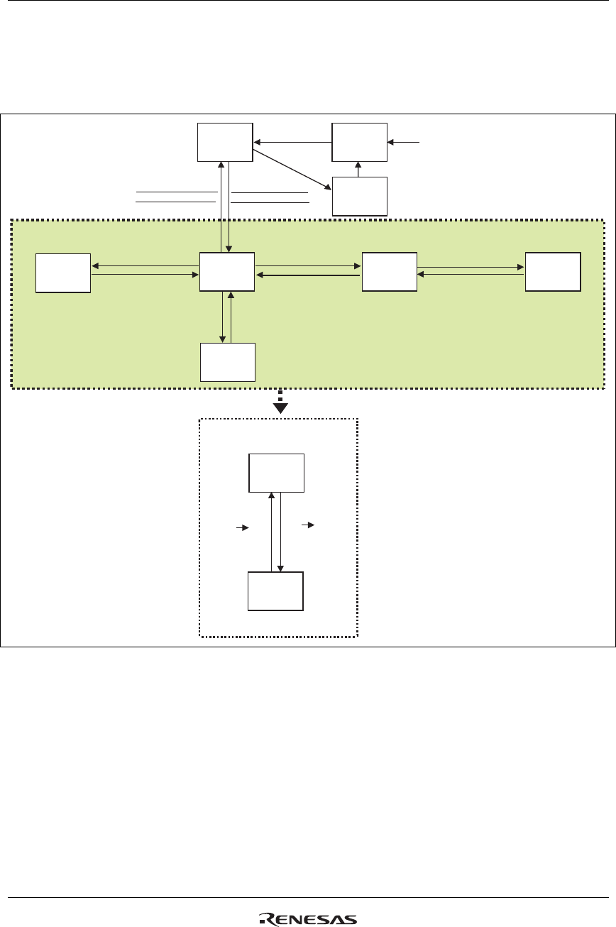
R61509V Target Spec
Rev. 0.11 April 25, 2008, page 95 of 181
Basic Mode Operation of the R61509V
The basic operation modes of the R61509V are shown in the following diagram. When making a transition
from one mode to another, refer to instruction setting sequence.
Reset
state
Display
OFF
Internal clock
display
operation
VSYNC
interface
RGB
interface (1)
RGB
interface (2)
Initial setting
Display ON sequence
(Power ON sequence)
VSYNC i/F sequence 2
(DM=10, RM=0)
RGB i/F (2) sequence 1
(DM=01, RM=0)
moving picture
display
RAM access via
system i/F while displaying
moving picture
moving picture
display
262k-color
mode
8-color
mode
Partial
display
Display color control
262k 8
color display
sequence
8 262k
color display
sequence
Exit shut down mode
Shut down
mode
DSTB = 1
Deep
standby set
RGB i/F (2) sequence 2
(DM=01, RM=1)
VSYNC i/F sequence 1
(DM=00, RM=0)
RGB i/F (1) sequence 1
(DM=01, RM=1)
RGB i/F (1) sequence 2
(DM=00, RM=0)
Partial
display
sequence 2
Partial
display
sequence 1
Display OFF sequence
(Power OFF sequence)
Reset
Figure 12

R61509V Target Spec
Rev. 0.11 April 25, 2008, page 96 of 181
Interface and Data Format
The R61509V supports system interface for making instruction and other settings, and external display
interface for displaying a moving picture. The R61509V can select the optimum interface for the display
(moving or still picture) in order to transfer data efficiently.
As external display interface, the R61509V supports RGB interface and VSYNC interface, which enables
data rewrite operation without flickering the moving picture on display.
In RGB interface operation, the display operation is executed in synchronization with synchronous signals
VSYNCX, HSYNCX, and DOTCLK. In synchronization with these signals, the R61509V writes display
data according to data enable signal (ENABLE) via RGB data signal bus (DB17-0). The display data is
stored in the R61509V’s GRAM so that data is transferred only when rewriting the frames of moving
picture and the data transfer required for moving picture display can be minimized. The window address
function specifies the RAM area to write data for moving picture display, which enables displaying a
moving picture and RAM data in other than the moving picture area simultaneously. To access the
R61509V’s internal RAM in high speed with low power consumption, use high-speed write function
(HWM = 1) in RGB or VSYNC interface operation.
In VSYNC interface operation, the internal display operation is synchronized with the frame
synchronization signal (VSYNCX). The VSYNC interface enables a moving picture display via system
interface by writing the data to the GRAM at faster than the minimum calculated speed in synchronization
with the falling edge of VSYNCX. In this case, there are restrictions in setting the frequency and the
method to write data to the internal RAM.
The R61509V operates in either one of the following four modes according to the state of the display. The
operation mode is set in the external display interface control register (R0Ch). When switching from one
mode to another, make sure to follow the relevant sequence in setting instruction bits.
Table 56 Operation Modes
Operation Mode RAM Access Setting (RM) Display Operation Mode (DM)
Internal clock operation
(displaying still pictures)
System interface
(RM = 0)
Internal clock operation
(DM1-0 = 00)
RGB interface (1)
(displaying moving pictures)
RGB interface
(RM = 1)
RGB interface
(DM1-0 = 01)
RGB interface (2)
(rewriting still pictures while
displaying moving pictures)
System interface
(RM = 0)
RGB interface
(DM1-0 = 01)
VSYNC interface
(displaying moving pictures)
System interface
(RM = 0)
VSYNC interface
(DM1-0 = 10)
Notes: 1. Instructions are set only via system interface.
2. When RGB interface is used, instructions should be transferred via clock synchronous serial
interface.
3. RGB and VSYNC interfaces cannot be used simultaneously.
4. Do not make changes to the RGB interface operation setting (RIM1-0) while RGB interface is
in operation.
5. See the “External Display Interface” section for the sequences when switching from one mode
to another.
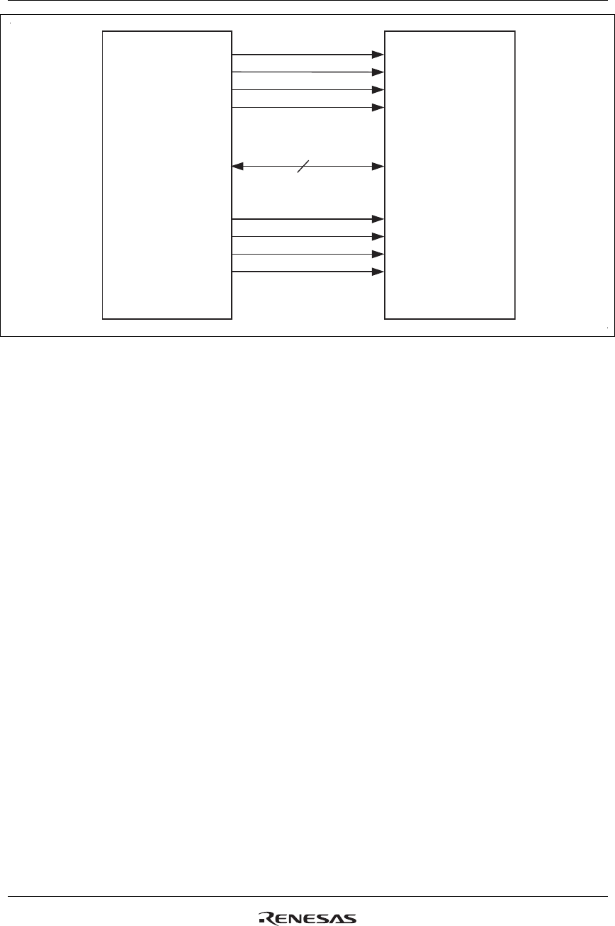
R61509V Target Spec
Rev. 0.11 April 25, 2008, page 97 of 181
CSX
RS
WRX
R61509V
System interface
18/16/9/8
RGB interface
18/16
DB17-0
(RDX)
ENABLE
VSYNCX
HSYNCX
DOTCLK
System
interface
RGB
interface
System
Figure 13
Internal clock operation
The display operation is synchronized with signals generated from internal oscillator’s clock (OSC) in this
mode. All input via external display interface is disabled in this operation. The internal RAM can be
accessed only via system interface.
RGB interface operation (1)
The display operation is synchronized with frame synchronous signal (VSYNCX), line synchronous signal
(HSYNCX), and dot clock signal (DOTCLK) in RGB interface operation. These signals must be supplied
during the display operation via RGB interface.
The R61509V transfers display data in units of pixels via DB17-0 pins. The display data is stored in the
internal RAM. The combined use of window address function can minimize the total number of data
transfer for moving picture display by transferring only the data to be written in the moving picture RAM
area when it is written and enables the R61509V to display a moving picture and the data in other than the
moving picture RAM area simultaneously.
The front porch (FP), back porch (BP), and the display (NL) periods are automatically calculated inside the
R61509V by counting the number of clocks of line synchronous signal (HSYNCX) from the falling edge of
the frame synchronous signal (VSYNCX). Make sure to transfer pixel data via DB17-0 pins in accordance
with the setting of these periods.

R61509V Target Spec
Rev. 0.11 April 25, 2008, page 98 of 181
RGB interface operation (2)
This mode enables the R61509V to rewrite RAM data via system interface while using RGB interface for
display operation. To rewrite RAM data via system interface, make sure that display data is not transferred
via RGB interface (ENABLE = high). To return to the RGB interface operation, change the ENABLE
setting first. Then set an address in the RAM address set register and R22h in the index register.
VSYNC interface operation
The internal display operation is synchronized with the frame synchronous signal (VSYNCX) in this mode.
This mode enables the R61509V to display a moving picture via system interface by writing data in the
internal RAM at faster than the calculated minimum speed via system interface from the falling edge of
frame synchronous (VSYNCX). In this case, there are restrictions in speed and method of writing RAM
data. For details, see the “VSYNC Interface” section.
As external input, only VSYNCX signal input is valid in this mode. Other input via external display
interface becomes disabled.
The front porch (FP), back porch (BP), and the display (NL) periods are automatically calculated from the
frame synchronous signal (VSYNCX) inside the R61509V according to the instruction settings for these
periods.
FMARK interface operation
In the FMARK interface operation, data is written to internal RAM via system interface synchronizing with
the frame mark signal (FMARK), realizing tearing-less moving picture while using conventional system
interface. In this case, there are restrictions in speed and method of writing RAM data. See “FMARK
interface” for detail.

R61509V Target Spec
Rev. 0.11 April 25, 2008, page 99 of 181
System Interface
The following are the kinds of system interfaces available with the R61509V. The interface operation is
selected by setting the IM2/1/0 pins. The system interface is used for instruction setting and RAM access.
Table 57 IM Bit Settings and System Interface
IM2 IM1 IM0 Interfacing Mode with Host Processor DB Pins Colors
0 0 0 80-system 18-bit interface DB17-0 262,144
0 0 1 80-system 9-bit interface DB17-9 262,144
0 1 0 80-system 16-bit interface DB17-10, DB8-1 262,144
*see Note1
0 1 1 80-system 8-bit interface DB17-10 262,144
*see Note2
1 0 * Clock synchronous serial interface - 65,536
1 1 0 Setting inhibited - -
1 1 1 Setting inhibited - -
Notes: 1. 65,536 colors in 16-bit single transfer mode.
2. 262,144 colors is 8-bit 3-transfer mode. 65,536 colors in 8-bit 2-transfer mode.
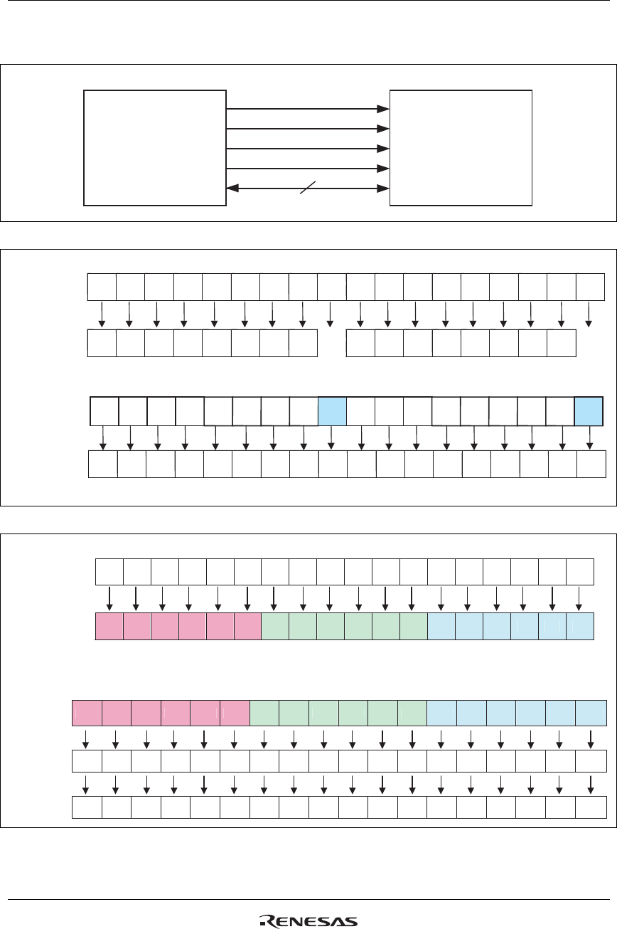
R61509V Target Spec
Rev. 0.11 April 25, 2008, page 100 of 181
80-System 18-bit Bus Interface
A1
HWR
RS
WRX
18
R61509V
HOST
PROCESSOR
IM[2:0] = 000
CSn
(RDX) (RDX)
D31-0
CSX
DB17-0
Figure 14 18-bit Interface
Instruction write
DB
17
DB
16
DB
15
DB
14
DB
13
DB
12
DB
11
DB
10
DB
9
DB
8
DB
7
DB DB
5
DB
4
DB
3
DB
2
DB
1
DB
0
IB
15
IB IB
13
IB
12
IB
11
IB
10
IB
9
IB
8
IB
7
IB
6
IB
5
IB
4
IB
3
IB
2
IB
1
IB
0
14
6
Device code read / Instruction read
DB
17
DB
16
DB
15
DB
14
DB
13
DB
12
DB
11
DB
10
DB
9
DB
8
DB
7
DB DB
5
DB
4
DB
3
DB
2
DB
1
DB
0
IB
15
IB IB
13
IB
12
IB
11
IB
10
IB
9
IB
8
IB
7
IB
6
IB
5
IB
4
IB
3
IB
2
IB
1
IB
0
14
6
Instruction code
Instruction code
Input
Instruction
Device code
Output
Figure 15 18-bit Interface Data Format (Instruction Write / Device Code Read / Instruction Read)
DB
17
DB DB DB
14
DB
13
DB
12
DB
11
DB
10
DB
9
DB
8
DB DB
6
DB
5
DB
4
DB
3
DB
2
DB
1
DB
0
R5 R4 R3 R2 R1 R0 G5 G4 G3 G2 G1 G0 B5 B4 B3 B2 B1 B0
RAM data write
7
16 15
RAM data read
GRAM write
data
Input
R5 R4 R3 R2 R1 R0 G5 G4 G3 G2 G1 G0 B5 B4 B3 B2 B1 B0
RD
[17]
RD
[16]
RD
[15]
RD
[14]
RD
[13]
RD
[12]
RD
[11]
RD
[10]
RD
[9]
RD
[8]
RD
[7]
RD
[6]
RD
[5]
RD
[4]
RD
[3]
RD
[2]
RD
[1]
RD
[0]
DB
17
DB
16
DB
15
DB
14
DB
13
DB
12
DB
11
DB
10
DB
9
DB
8
DB
7
DB
6
DB
5
DB
4
DB
3
DB
2
DB
1
DB
0
GRAM data
Read data
Output pins
Note: Normal display in 262,144 colors.
1 pixel
Figure 16 18-bit Interface Data Format (RAM Data Write / RAM Data Read)
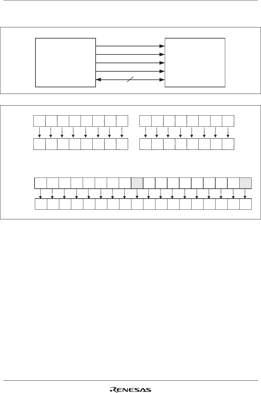
R61509V Target Spec
Rev. 0.11 April 25, 2008, page 101 of 181
80-System 16-bit Bus Interface
A1
HWR
RS
WR:
16
R61509V
HOST
PROCESSOR
IM[2:0] = 010
CSn
(RD:)(RD:)
D15-0
CS:
DB17-10, 8-1
Figure 17 16-bit Interface
Instruction
DB
17
DB
16
DB
15
DB
14
DB
13
DB
12
DB
11
DB
10
DB
8
DB
7
DB DB
5
DB
4
DB
3
DB
2
DB
1
IB
15
IB IB
13
IB
12
IB
11
IB
10
IB
9
IB
8
IB
7
IB
6
IB
5
IB
4
IB
3
IB
2
IB
1
IB
0
14
6
Instruction
Input
Instruction code
DB
17
DB
16
DB
15
DB
14
DB
13
DB
12
DB
11
DB
10
DB
9
DB
8
DB
7
DB DB
5
DB
4
DB
3
DB
2
DB
1
DB
0
IB
15
IB IB
13
IB
12
IB
11
IB
10
IB
9
IB
8
IB
7
IB
6
IB
5
IB
4
IB
3
IB
2
IB
1
IB
0
14
6
Instruction code
Device code read / Instruction read
Device code
Output
Note: Device code cannot be read in 2 transfer mode.
Figure 18 16-bit Interface Data Format (Instruction Write / Device Code Read / Instruction Read)
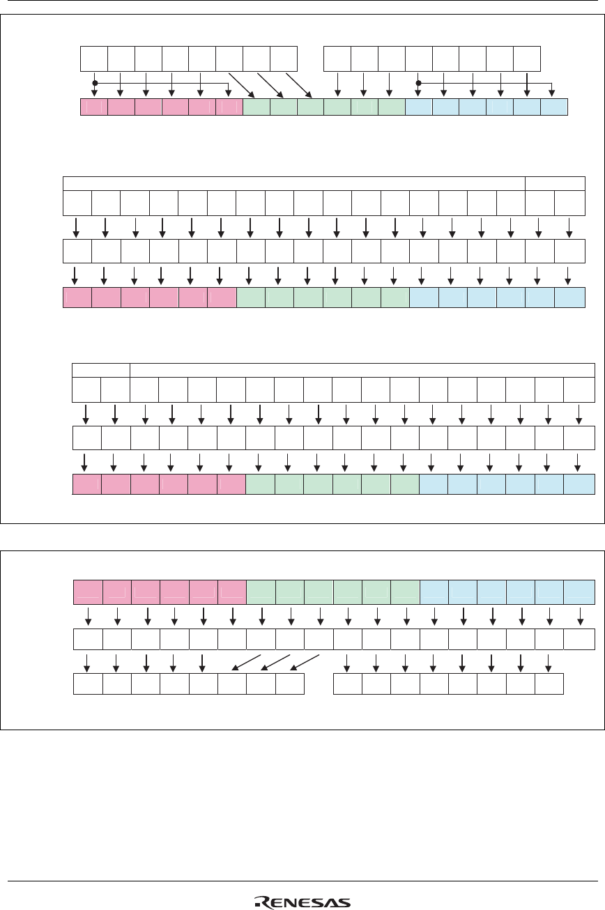
R61509V Target Spec
Rev. 0.11 April 25, 2008, page 102 of 181
1
DB
17
DB
6
DB
5
DB
14
DB
13
DB
12
DB
11
DB
10
DB
8
DB DB
6
DB
5
DB
4
DB
3
DB
2
DB
1
R5 R4 R3 R2 R1 R0 G5 G4 G3 G2 G1 G0 B5 B4 B3 B2 B1 B0
RAM data write (1-transfer mode: TRI = 0)
17
Note: 65,536 colors are available.
Input
1 pixel
DB
17
DB
16
DB
15
DB
14
DB
13
DB
12
DB
11
DB
10
DB
8
DB
7
DB
6
DB
5
DB
4
DB
3
DB
2
DB
1
DB
17
DB
16
WD
[17]
WD
[16]
WD
[15]
WD
[14]
WD
[13]
WD
[12]
WD
[11]
WD
[10]
WD
[9]
WD
[8]
WD
[7]
WD
[6]
WD
[5]
WD
[4]
WD
[3]
WD
[2]
WD
[1]
WD
[0]
R5 R4 R3 R2 R1 R0 G5 G4 G3 G2 G1 G0 B5 B4 B3
B2 B1 B0
Note: Normal display in 262,144 colors.
First transfer Second transfer
RAM data write (2-transfer mode: TRI = 0, DFM = 0)
RGB
assignment
GRAM
write data
1 pixel
Input
pins
DB
2
DB
1
DB
17
DB
16
DB
15
DB
14
DB
13
DB
12
DB
11
DB
10
DB
8
DB
7
DB
6
DB
5
DB
4
DB
3
DB
2
DB
1
WD
[17]
WD
[16]
WD
[15]
WD
[14]
WD
[13]
WD
[12]
WD
[11]
WD
[10]
WD
[9]
WD
[8]
WD
[7]
WD
[6]
WD
[5]
WD
[4]
WD
[3]
WD
[2]
WD
[1]
WD
[0]
R5 R4 R3 R2 R1 R0 G5 G4 G3 G2 G1 G0 B5 B4 B3
B2 B1 B0
RAM data write (2-transfer mode: TRI = 1, DFM = 1)
Note: Normal display in 262,144 colors.
1 pixel
First transfer Second transfer
GRAM write
data
RGB
assignment
Input pins
(EPE=2'h0)
Figure 19 16-bit Interface Data Format (RAM Data Write)
R5 R4 R3 R2 R1 R0 G5 G4 G3 G2 G1 G0 B5 B4 B3 B2 B1 B0
RD
[17]
RD
[16]
RD
[15]
RD
[14]
RD
[13]
RD
[12]
RD
[11]
RD
[10]
RD
[9]
RD
[8]
RD
[7]
RD
[6]
RD
[5]
RD
[4]
RD
[3]
RD
[2]
RD
[1]
RD
[0]
DB
17
DB
16
DB
15
DB
14
DB
13
DB
12
DB
11
DB
10 DB
8
DB
7
DB
6
DB
5
DB
4
DB
3
DB
2
DB
1
RAM data read (1-transfer mode: TRI = 0)
GRAM data
Read data
Output pins
Note: RAM data cannot be read in 2-transfer mode.
Figure 20 16-bit Interface Data Format (RAM Data Read)
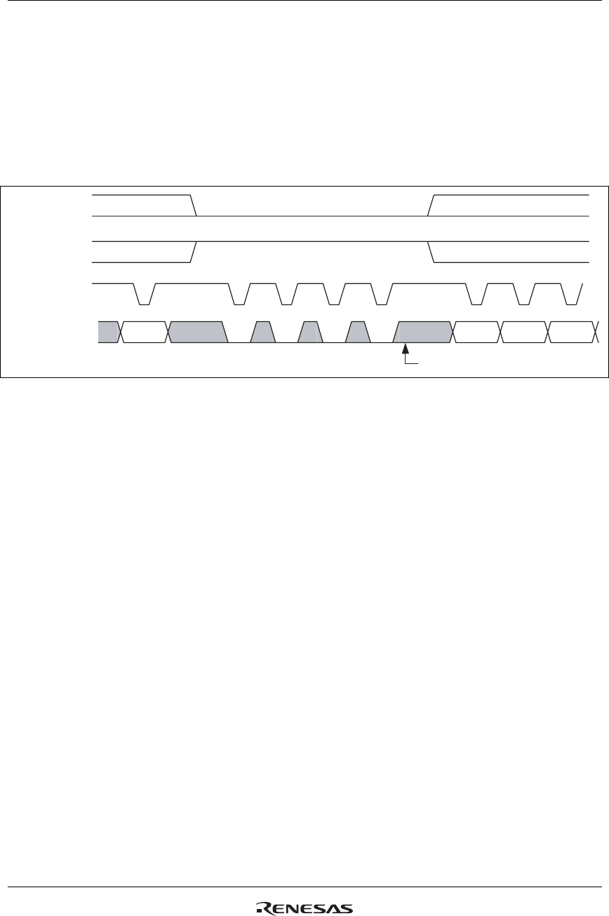
R61509V Target Spec
Rev. 0.11 April 25, 2008, page 103 of 181
Data Transfer Synchronization in 16-bit Bus Interface Operation
The R61509V supports data transfer synchronization function to reset the counters for upper 16-/2-bit and
lower 2-/16-bit transfers in 16-bit 2-transfer mode. When a mismatch occurs in upper and lower data
transfers due to noise and so on, the 000H instruction is written four times consecutively to reset the upper
and lower counters in order to restart the data transfer from upper 2/16 bits. The data transfer
synchronization, when executed periodically, can help the display system recover from runaway.
Make sure to execute data transfer synchronization after reset operation before transferring instruction.
WRX
RDX
RS
(16-bit transfer synchronization)
DB17 ~ DB10,
DB8 ~ DB1
Upper
Lower
Upper UpperLower
"000"H"000"H"000"H"000"H
Figure 21 16-bit Data Transfer Synchronization
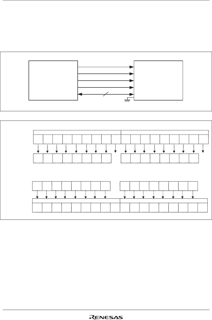
R61509V Target Spec
Rev. 0.11 April 25, 2008, page 104 of 181
80-System 9-bit Bus Interface
When transferring 16-bit instruction, it is divided into upper and lower 8 bits, and the upper 8 bits are
transferred first (the LSB is not used). The RAM write data is also divided into upper and lower 9 bits, and
the upper 9 bits are transferred first. The unused DB pins must be fixed at either IOVCC or IOGND level.
When transferring the index register setting, make sure to write upper byte (8 bits).
A1
HWR
RS
WR:
9
9
R61509V
HOST
PROCESSOR
IM[2:0] = 001
CSn
(RDX) (RD:)
D15-0
CS:
DB17-9
DB8-0
Figure 22 9-bit Interface
DB
17
DB
16
DB
15
DB
14
DB
13
DB
12
DB
11
DB
10
DB
9
DB
17
DB
16
DB
15
DB
14
DB
13
DB
12
DB
11
DB
10
DB
9
IB
15
IB IB
13
IB
12
IB
11
IB
10
IB
9
IB
8
IB
7
IB
6
IB
5
IB
4
IB
3
IB
2
IB
1
IB
014
Instruction write
Input
Instruction
First transfer Second transfer
Instruction code
DB
17
DB
16
DB
15
DB
14
DB
13
DB
12
DB
11
DB
10
DB
9
DB
17
DB
16
DB
15
DB
14
DB
13
DB
12
DB
11
DB
10
DB
9
IB
15
IB IB
13
IB
12
IB
11
IB
10
IB
9
IB
8
IB
7
IB
6
IB
5
IB
4
IB
3
IB
2
IB
1
IB
0
14
First transfer Second transfer
Device code read / Instruction read
Instruction
Output
instruction code
Figure 23 9-bit Interface Data Format (Instruction Write / Device Code Read / Instruction Read)
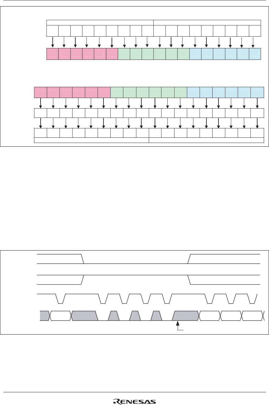
R61509V Target Spec
Rev. 0.11 April 25, 2008, page 105 of 181
DB
17
DB
16
DB
15
DB
14
DB
13
DB
12
DB
11
DB
10
DB
9
DB
17
DB
6
DB
5
DB
14
DB
13
DB
12
DB
11
DB
10
DB
9
R5 R4 R3 R2 R1 R0 G5 G4 G3 G2 G1 G0 B5 B4 B3 B2 B1 B0
R5 R4 R3 R2 R1 R0 G5 G4 G3 G2 G1 G0 B5 B4 B3 B2 B1 B0
RD
[17]
RD
[16]
RD
[15]
RD
[14]
RD
[13]
RD
[12]
RD
[11]
RD
[10]
RD
[9]
RD
[8]
RD
[7]
RD
[6]
RD
[5]
RD
[4]
RD
[3]
RD
[2]
RD
[1]
RD
[0]
DB
17
DB
16
DB
15
DB
14
DB
13
DB
12
DB
11
DB
10
DB
9
DB
17
DB
16
DB
15
DB
14
DB
13
DB
12
DB
11
DB
10
DB
9
First transfer Second transfer
RAM data write
RAM read data
1 pixel
GRAM data
Input
GRAM write
data
Read data
Output pins
First transfer Second transfer
Note: Normal display in 262,144 colors.
Figure 24 9-bit Interface Data Format (RAM Data Write/ RAM Data Read)
Data Transfer Synchronization in 9-bit Bus Interface Operation
The R61509V supports data transfer synchronization function to reset the counters for upper and lower 9-
bit transfers in 9-bit bus transfer mode. When a mismatch occurs in upper and lower data transfers due to
noise and so on, the 00H instruction is written four times consecutively to reset the upper and lower
counters in order to restart the data transfer from upper 9 bits. The data transfer synchronization, when
executed periodically, can help the display system recover from runaway.
Make sure to execute data transfer synchronization after reset operation before transferring instruction.
WRX
RDX
RS
(9-bit transfer synchronization)
DB17 ~ DB9
Upper
Lower
UpperUpper Lower
"00"H "00"H "00"H "00"H
Figure 25 9-bit Data Transfer Synchronization
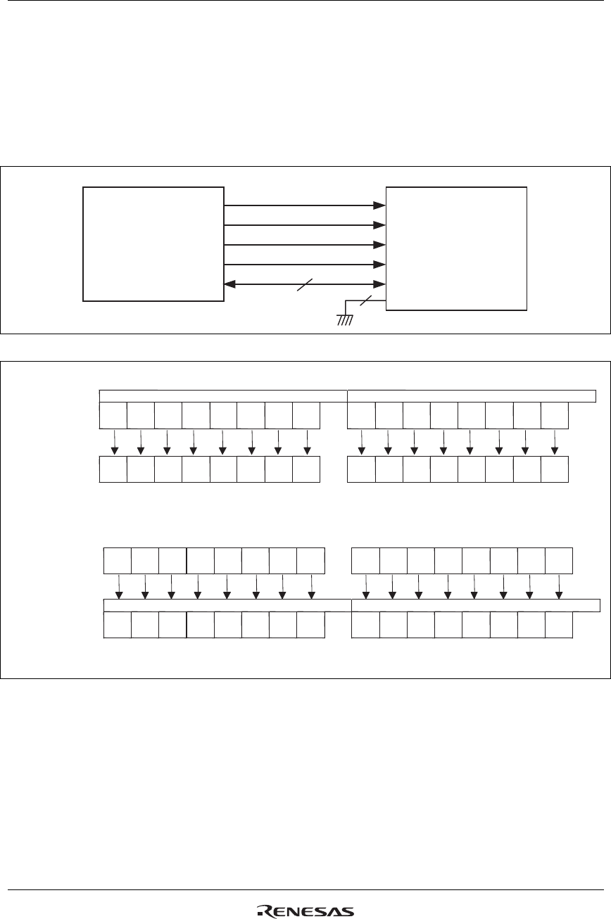
R61509V Target Spec
Rev. 0.11 April 25, 2008, page 106 of 181
80-System 8-bit Bus Interface
When transferring 16-bit instruction, it is divided into upper and lower 8 bits, and the upper 8 bits are
transferred first. The RAM write data is also divided into upper and lower 8 bits, and the upper 8 bits are
transferred first. The RAM write data is expanded into 18 bits internally as shown below. The unused DB
pins must be fixed at either IOVCC1 or GND level. When transferring the index register setting, make sure
to write upper byte (8 bits).
A1
HWR
HOST
PROCESSOR
CSX
RS
WRX
R61509V
8
10
IM[2:0] = 001
CSn
(RDX(RDX
D15-0 DB17-10
DB9-0
Figure 26 8-bit Interface
DB
17
DB
16
DB
15
DB
14
DB
13
DB
12
DB
11
DB
10
DB
17
DB
16
DB
15
DB
14
DB
13
DB
12
DB
11
DB
10
IB
15
IB
14
IB
13
IB
12
IB
11
IB
10
IB
9
IB
8
IB
7
IB
6
IB
5
IB
4
IB
3
IB
2
IB
1
IB
0
Instruction write
Input
Instruction
Instruction code
First transfer Second transfer
IB
15
IB
14
IB
13
IB
12
IB
11
IB
10
IB
9
IB
8
IB
7
IB
6
IB
5
IB
4
IB
3
IB
2
IB
1
IB
0
DB
17
DB
16
DB
15
DB
14
DB
13
DB
12
DB
11
DB
10
DB
17
DB
16
DB
15
DB
14
DB
13
DB
12
DB
11
DB
10
Device code read / Instruction read
Instruction
Input
First transfer Second transfer
Note: Device code canot be read out in 3 transfer mode.
Figure 27 8-bit Interface Data Format (Instruction Write / Device Code Read / Instruction Read)
Note: RAM data cannot be read in the 3-transfer mode.
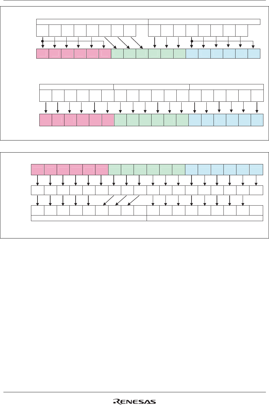
R61509V Target Spec
Rev. 0.11 April 25, 2008, page 107 of 181
DB
17
DB
16
DB
15
DB
14
DB
13
DB
12
DB
11
DB
10
DB
17
DB
16
DB
15
DB
14
DB
13
DB
12
DB
11
DB
10
R5 R4 R3 R2 R1 R0 G5 G4 G3 G2 G1 G0 B5 B4 B3 B2 B1 B0
RAM data write (2-transfer mode: TRI = 0)
Input
First transfer Second transfer
Note: Normal display in 65,536 colors.
1 pixel
DB
17
DB
16
DB
15
DB
14
DB
13
DB
12
DB
17
DB
16
DB
15
DB
14
DB
13
DB
12
DB
17
DB
16
DB
15
DB
14
DB
13
DB
12
R5 R4 R3 R2 R1 R0 G5 G4 G3 G2 G1 G0 B5 B4 B3 B2 B1 B0
RAM data write (3-transfer mode: TRI = 1, DFM = 1)
First transfer Second transfer Third transfer
Note: Normal display in 262,144 colors.
1 pixel
Input
GRAM write
data
Figure 28 8-bit Interface Data Format (RAM Data Write)
R5 R4 R3 R2 R1 R0 G5 G4 G3 G2 G1 G0 B5 B4 B3 B2 B1 B0
RD
[17]
RD
[16]
RD
[15]
RD
[14]
RD
[13]
RD
[12]
RD
[11]
RD
[10]
RD
[9]
RD
[8]
RD
[7]
RD
[6]
RD
[5]
RD
[4]
RD
[3]
RD
[2]
RD
[1]
RD
[0]
DB
17
DB
16
DB
15
DB
14
DB
13
DB
12
DB
11
DB
10
DB
17
DB
16
DB
15
DB
14
DB
13
DB
12
DB
11
DB
10
RAM data read
First transfer Second transfer
Note: RAM data cannot be read in 3-transfer mode.
GRAM data
Read data
Output pins
Figure 29 8-bit Interface Data Format (RAM Data Read)
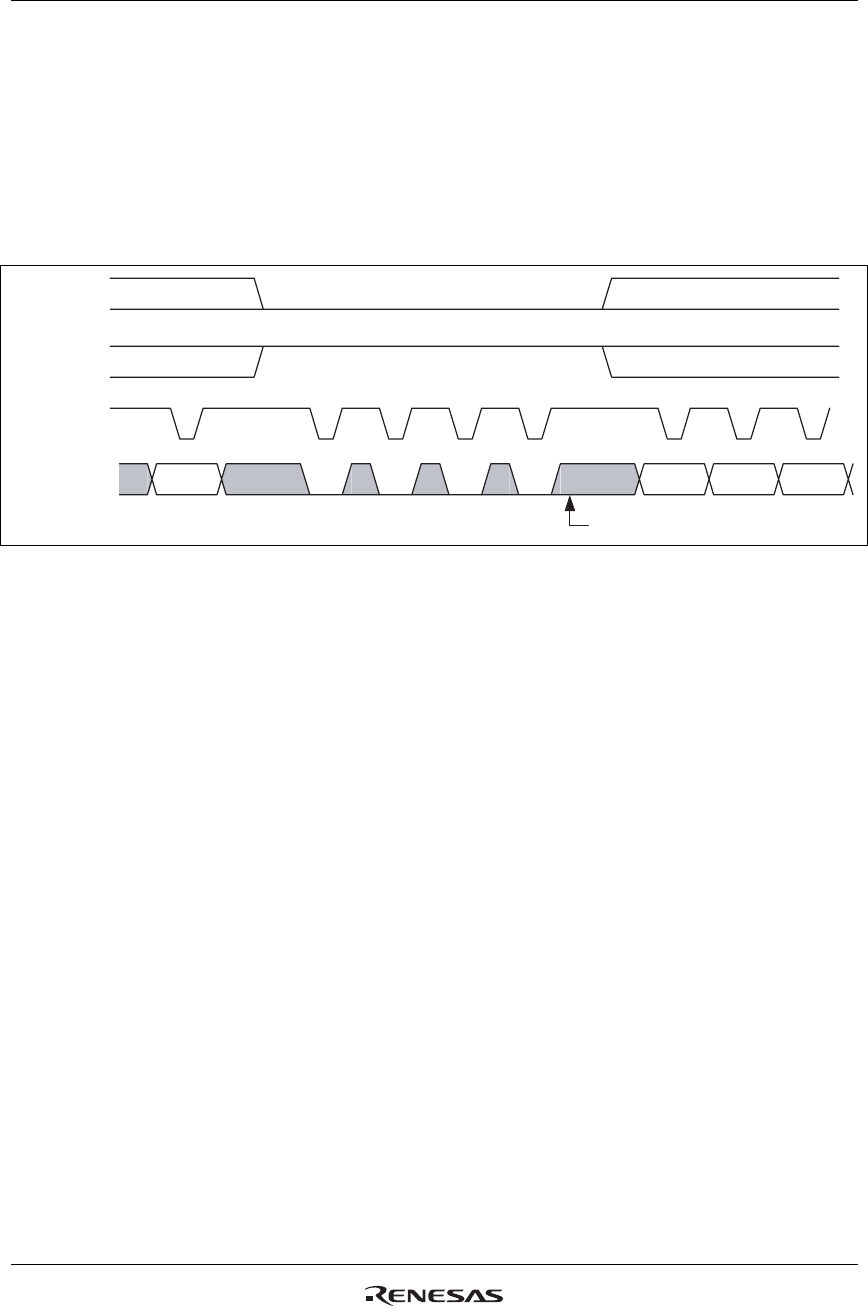
R61509V Target Spec
Rev. 0.11 April 25, 2008, page 108 of 181
Data Transfer Synchronization in 8-bit Bus Interface operation
The R61509V supports data transfer synchronization function to reset the counters for upper and lower 8-
bit transfers in 8-bit bus transfer mode. When a mismatch occurs in upper and lower data transfers due to
noise and so on, the 00H instruction is written four times consecutively to reset the upper and lower
counters in order to restart the data transfer from upper 8 bits. The data transfer synchronization, when
executed periodically, can help the display system recover from runaway.
Make sure to execute data transfer synchronization after reset operation before transferring instruction.
DB17 ~ DB10
WRX
RDX
RS
(8-bit transfer synchronization)
Upper
Lower Upper UpperLower
"00"H"00"H"00"H"00"H
Figure 30 8-bit Data Transfer Synchronization

R61509V Target Spec
Rev. 0.11 April 25, 2008, page 109 of 181
Serial Interface
The serial interface is selected by setting the IM2/1 pins to the IOVCC/GND levels, respectively. The data
is transferred via chip select line (CS), serial transfer clock line (SCL), serial data input line (SDI), and
serial data output line (SDO). In serial interface operation, the IM0_ID pin functions as the ID pin, and the
DB17-0 pins, not used in this mode, must be fixed at either IOVCC or GND level.
The R61509V recognizes the start of data transfer on the falling edge of CSX input and starts transferring
the start byte. It recognizes the end of data transfer on the rising edge of CSX input. The R61509V is
selected when the 6-bit chip address in the start byte transferred from the transmission unit and the 6-bit
device identification code assigned to the R61509V are compared and both 6-bit data match. Then, the
R61509V starts taking in subsequent data. The least significant bit of the device identification code is
determined by setting the ID pin. Send "01110” to the five upper bits of the device identification code.
Two different chip addresses must be assigned to the R61509V because the seventh bit of the start byte is
register select bit (RS). When RS = 0, index register write operation is executed. When RS = 1, either
instruction write operation or RAM read/write operation is executed. The eighth bit of the start byte is R/W
bit, which selects either read or write operation. The R61509V receives data when the R/W = 0, and
transfers data when the R/W = 1.
When writing data to the GRAM via serial interface, the data is written to the GRAM after it is transferred
in two bytes. The R61509V writes data to the GRAM in units of 18 bits by adding the same bits as the
MSBs to the LSB of R and B dot data.
After receiving the start byte, the R61509V starts transferring or receiving data in units of bytes. The
R61509V transfers data from the MSB. The R61509V’s instruction consists of 16 bits and it is executed
inside the R61509V after it is transferred in two bytes (16 bits: DB15-0) from the MSB. The R61509V
expands RAM write data into 18 bits when writing them to the internal GRAM. The first byte received by
the R61509V following the start byte is recognized as the upper eight bits of instruction and the second
byte is recognized as the lower 8 bits of instruction.
When reading data from the GRAM, valid data is not transferred to the data bus until first five bytes of data
are read from the GRAM following the start byte. The R61509V sends valid data to the data bus when it
reads the sixth and subsequent byte data.
Table 58 Start Byte Format
Transferred Bits S 1 2 3 4 5 6 7 8
Start byte format Transfer start Device ID code
0 1 1 1 0 ID
RS R/W
Note: The ID bit is determined by setting the IM0_ID pin.
Table 59 Functions of RS, R/W Bits
RS R/W Function
0 0 Set index register
0 1 Setting inhibited
1 0 Write instruction or RAM data
1 1 Read instruction or RAM data
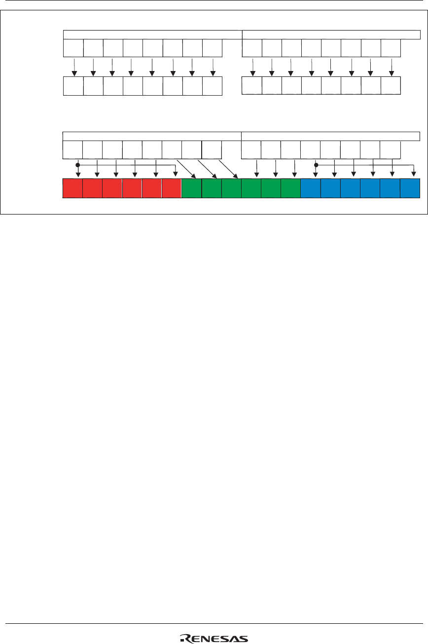
R61509V Target Spec
Rev. 0.11 April 25, 2008, page 110 of 181
First transfer (upper) Sec on d t ransfer (lower)
D
15
D
14
D
13
D
12
D
11
D
10 D9 D8 D7 D6 D5 D4 D3 D2 D1 D0
IB
15
IB
14
IB
13
IB
12
IB
11
IB
10
IB
9
IB
8
IB
7
IB
6
IB
5
IB
4
IB
3
IB
2
IB
1
IB
0
RAM data write
First tran sfer (upper) Sec on d t ransfer (lower)
D
0
D
7
D
6
D
5
D
4
D
3
D
2
D
1
R5 R4 R3 R2 R1 R0 G5 G4 G3 G2 G1 G0 B5 B4 B3 B2 B1 B5
1 pixel
D
15
D
14
D
13
D
12
D
11
D
10
D
9
D
8
Instruction
Instruction code
Instruction
Input
Input
GRAM write data
Note: 65,536-color display in SPI
Figure 31 Serial Interface Data Format
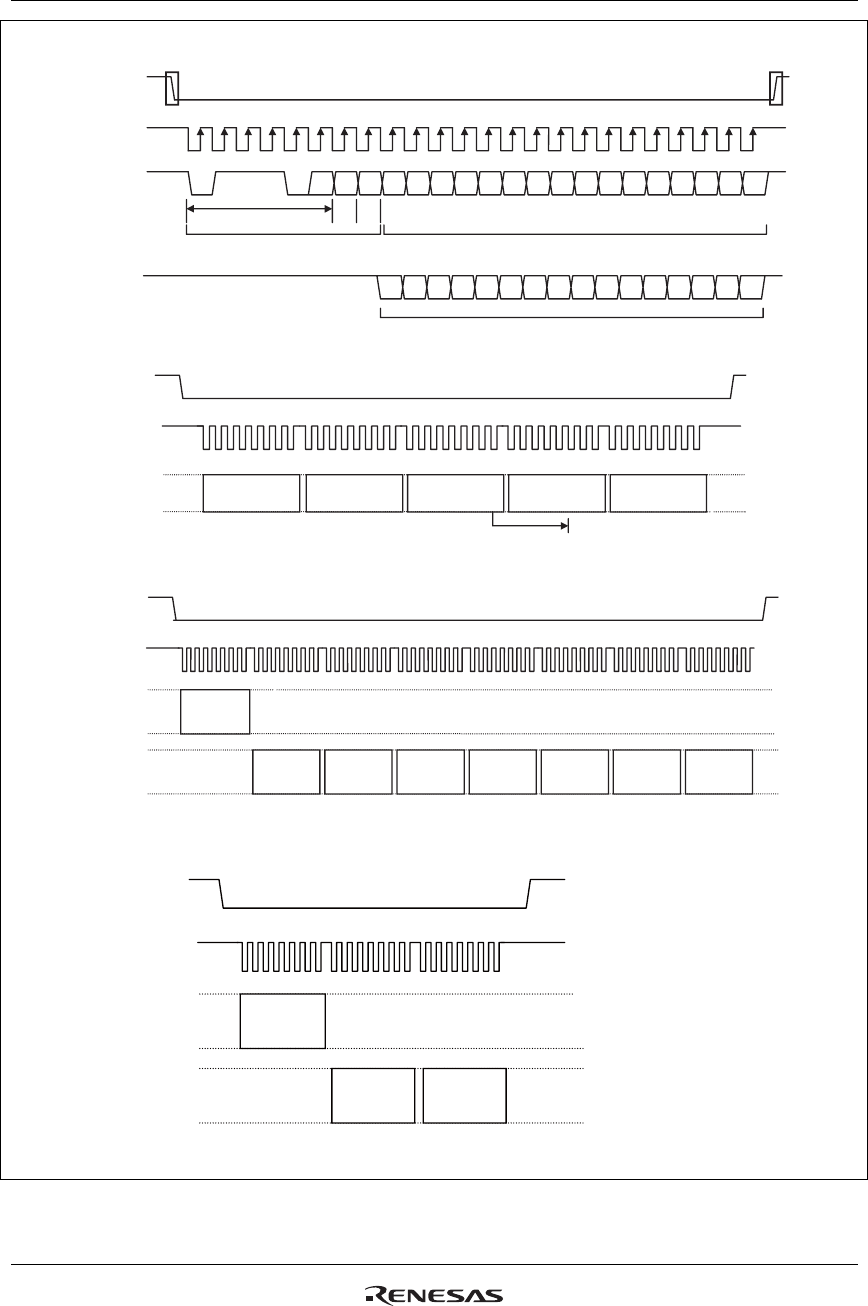
R61509V Target Spec
Rev. 0.11 April 25, 2008, page 111 of 181
D0
LSB
1
“0” “1” “1” “1” “0” ID RS RW D15 D14 D13 D12 D11 D10 D9 D8 D7 D6 D5 D4 D3 D2 D1
23 4 5 6 7 8 9 101112131415161718192021222324
Device ID code RS RW
MSB
Transfer start End of transfe
r
D0D15 D14 D13 D12 D11 D10 D9 D8 D7 D6 D5 D4 D3 D2 D1
Start byte Instruction (1)
Upper 8 bits
Instruction (1)
Lower 8 bits
Instruction
execution time (1)
Dummy read
1
Dummy read
2
Dummy read
3
Dummy read
4
Dummy read
5
(a) Clock synchronization serial data transfer (basic mode)
(b) Clock synchronization serial consecutive data transfer
(c) RAM read data transfer
Instruction rea
d
L
ower
8
bits
Note: The eight bits read after start byte input is recognized
as the upper byte of instruction.
Note: Valid data is not sent until the R61509V reads five bytes from the GRAM after start byte input .
The R61509V sends valid data when it reads the sixth and subsequent bytes.
RAM read
Upper 8 bits
RAM read
Lower 8 bits
CSX
input
SCL
input
SDI
input
SDO
output
Start End
CSX
input
SCL
input
SDI
input
CSX
input
SCL
input
SDI
input
SDO
output
Start End
Instruction (2)
Upper 8 bits
Instruction (2)
Lower 8 bits
Read instruction, RAM data
Set IR (index register), instruction, write RAM data
Start byte
RS = 1
R/W = 1
Start byte
RS=0
R/W=1
CSX
input
SCL
input
SDI
input
SDO
output
Start byte
Instruction read
Upper 8 bits
Instruction read
Lower 8 bits
Start End
(d) Instruction read
Note: Valid RAM data is read out right after the start byte.
Figure 32 Data Transfer in Serial Interface
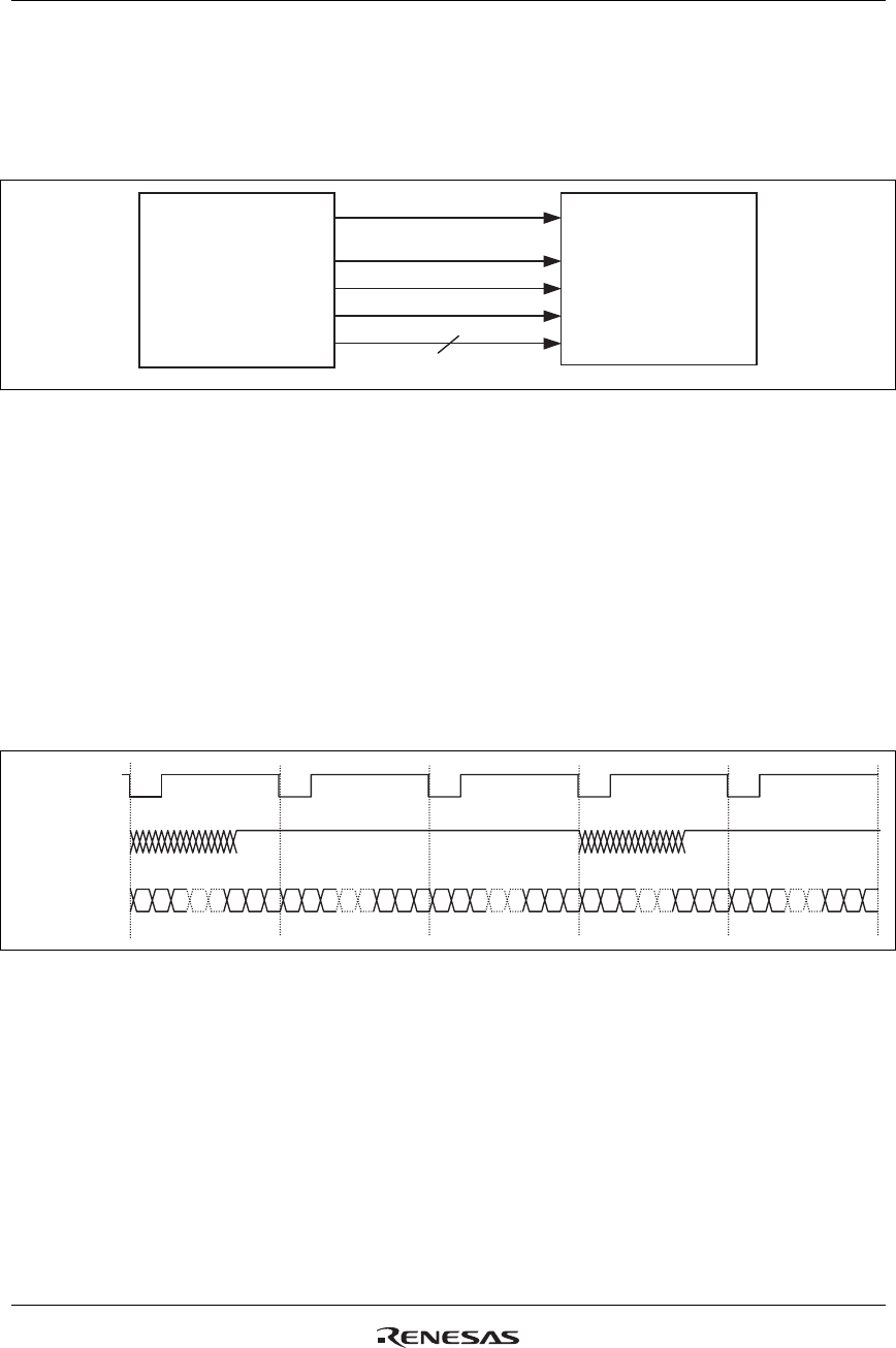
R61509V Target Spec
Rev. 0.11 April 25, 2008, page 112 of 181
VSYNC Interface
The R61509V supports VSYNC interface, which enables displaying a moving picture via system interface
by synchronizing the display operation with the VSYNCX signal. VSYNC interface can realize moving
picture display with minimum modification to the conventional system operation.
RS
WRX
16
R61509V
VSYNCX
CSX
DB17-0, 8-1
HOST
PROCESSOR
Figure 33 VSYNC Interface
The VSYNC interface is selected by setting DM1-0 = 10 and RM = 0. In VSYNC interface operation, the
internal display operation is synchronized with the VSYNCX signal. By writing data to the internal RAM
at faster than the calculated minimum speed (internal display operation speed + margin), it becomes
possible to rewrite the moving picture data without flickering the display and display a moving picture via
system interface.
The display operation is performed in synchronization with the internal clock signal generated from the
internal oscillator and the VSYNCX signal. The display data is written in the internal RAM so that the
R61509V rewrites the data only within the moving picture area and minimize the number of data transfer
required for moving picture display.
RAM data
write via
system interface
Display operation
synchronized with
internal clock
VSYNCX
Figure 34 Moving Picture Data Transfers via VSYNC Interface

R61509V Target Spec
Rev. 0.11 April 25, 2008, page 113 of 181
The VSYNC interface has the minimum for RAM data write speed and internal clock frequency, which
must be more than the values calculated from the following formulas, respectively.
iancevar)clocks(23))BP(BackPorch)FP(FrontPorch)NL(esDisplayLin(encyFrameFrequ
) [Hz] ency (fosclock frequInternal c
××++×=
fosc
1
)clocks(23)insargm)NL(esDisplayLin)BP(BackPorch(
)NL(esDisplayLin240
]Hz.)[(mineedRAMWriteSp
××−+
×
>
Note: When RAM write operation is not started right after the falling edge of VSYNCX, the time from
the falling edge of VSYNCX until the start of RAM write operation must also be taken into account.
An example of calculating minimum RAM writing speed and internal clock frequency in VSYNC interface
operation is as follows.
[Example]
Panel size 240 RGB × 432 lines (NL = 6’h35: 432 lines)
Total number of lines (NL) 432 lines
Back/front porch 14/2 lines (BP = 4h’E, FP = 4’h2)
Frame frequency 60 Hz
Internal clock frequency 678 kHz
Internal clock frequency (fosc) [Hz]
= 678 kHz × 1.07 / 1.0 = 726 kHz
Notes: 1. When setting the internal clock frequency, possible causes of fluctuation must also be taken into
consideration. In this example, the internal clock frequency allows for a margin of ±7% for
variances and guarantee that display operation is completed within one VSYNCX cycle.
2. This example includes variances attributed to LSI fabrication process and room temperature.
Other possible causes of variances, such as differences in voltage change are not considered in
this example. It is necessary to include a margin for these factors.
Minimum speed for RAM writing [Hz]
> 240 × 432 / {((14 + 432 - 2) lines × 23 clocks) × 1/726 kHz} = 7.4 MHz
Notes: 1. In this example, it is assumed that the R61509V starts writing data in the internal RAM on the
falling edge of VSYNCX.
2. There must be at least a margin of 2 lines between the line to which the R61509V has just
written data and the line where display operation on the LCD is performed.
In this example, the RAM write operation at a speed of 7.4 MHz or more, which starts on the falling edge
of VSYNCX, guarantees the completion of data write operation in a certain line address before the
R61509V starts the display operation of the data written in that line and can write moving picture data
without causing flicker on the display.
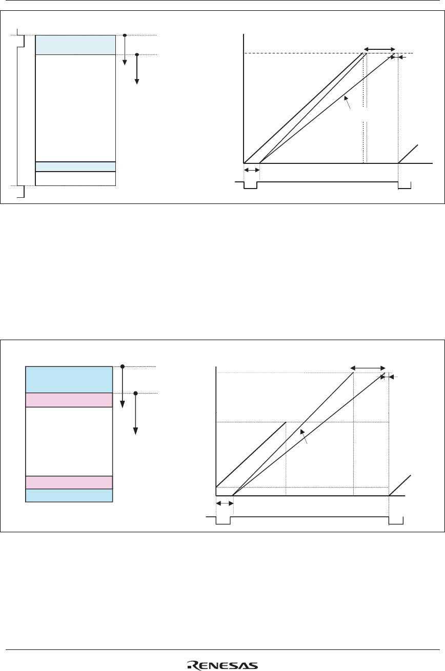
R61509V Target Spec
Rev. 0.11 April 25, 2008, page 114 of 181
RAM
write
Display
operation
016.67
(60 Hz)
Back porch
(14 lines)
Main panel
Moving picture
display
(432 lines)
Front porch (2 lines)
Blank period
RC oscillation
±7%
Display
operation
VSYNCX
[line]
432
VSYNCX
BP = 14H
RAM write
7.4 MHz
FP = 2H
[ms]
Line processing
Figure 35 Write/Display Operation Timing via VSYNC Interface
Notes to VSYNC Interface Operation
1. The above example of calculation gives a theoretical value. Possible causes of variances of internal
oscillator should be taken into consideration. Make enough margins in setting RAM write speed for
VSYNC interface operation.
2. The above example shows the values when writing over the full screen. Extra margin will be created if
the moving picture display area is smaller than that.
0
16.67
(60 Hz)
Display
operation
16
Back porch (14 lines)
Base image
Moving picture
display
(360 lines)
Front porch (2 lines)
(16 lines)
(56 lines)
RAM
write [line]
[ms]
432
376
BP = 14H
VS
YN
C
VSYNCX
FP = 2H
RC oscillation
±7%
Display
operation
RAM write
7.4MHz
Line processing
Figure 36 RAM Write Speed Margins
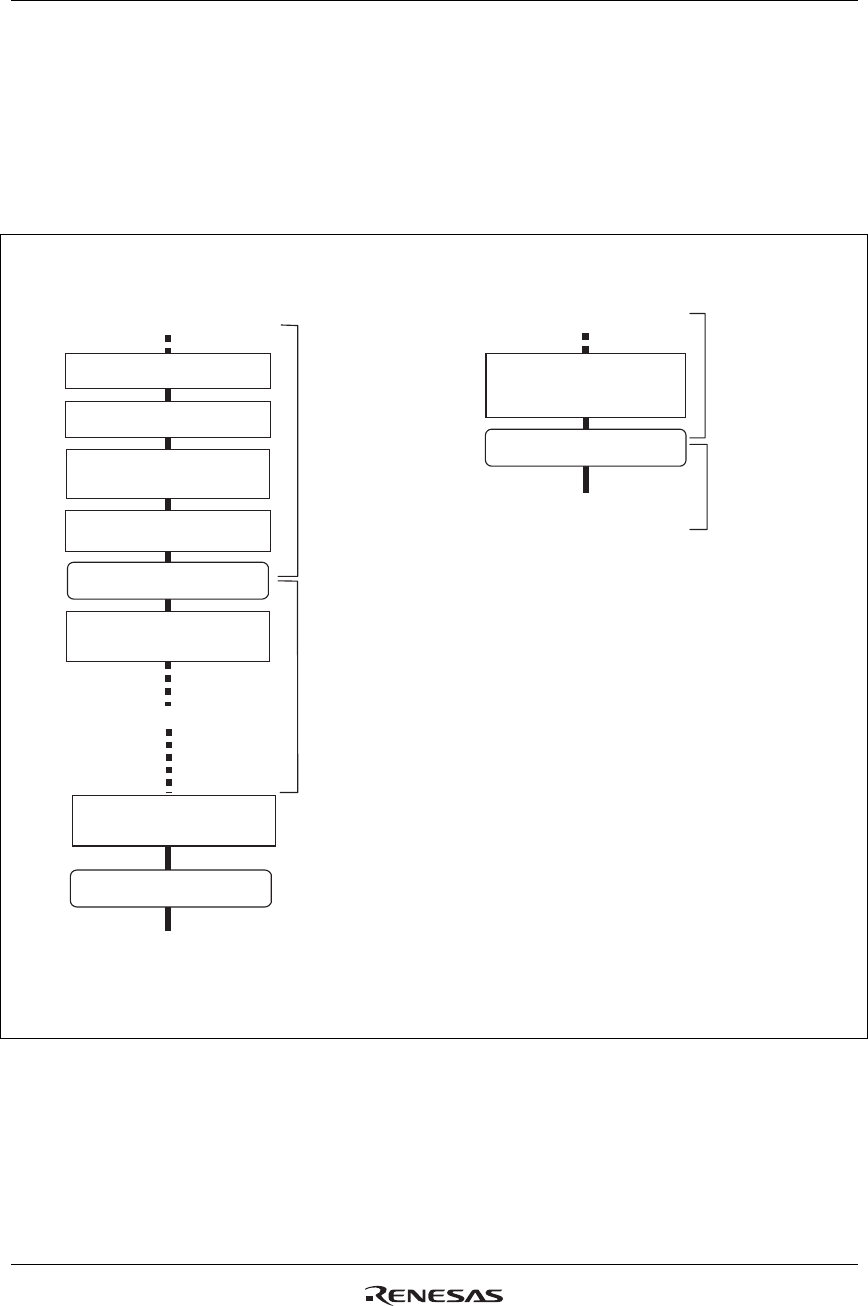
R61509V Target Spec
Rev. 0.11 April 25, 2008, page 115 of 181
3. The front porch period continues from the end of one frame period to the next VSYNCX input.
4. The instructions to switch from internal clock operation (DM1-0 = 00) to VSYNC interface operation
modes and vice versa are enabled from the next frame period.
5. The partial display and vertical scroll functions are not available in VSYNC interface operation.
6. In VSYNC interface operation, set AM = 0 to transfer display data correctly.
Internal Clock Operation to VSYNC Interface
Operation via VSYNC interface
VSYNC Interface to Internal Clock Operation
Internal clock operation
AM = 0
RAM address set
Set DM1-0 = 01 and RM = 0
for VSYNC interface
Write data to RAM
via VSYNC interface
Wait one frame period
or more
Set index register to R202h
Display operation in
synchronization with
internal clocks
VSYNC interface operation Display operation in
synchronization with
VSYNCX
Display operation in
synchronization with VSYNCX
Internal clock operation
Set internal clock
operation mode*
(DM1-0 = 00 and RM = 0)
Display operation in
synchronization with
internal clocks
Note: Continue VSYNC interface signals at least for
one frame period after setting DM1-0, RM bits
to internal clock operation.
Note: Input the VSYNC interface signals before setting the DM1-0 and RM bits
to the VSYNC interface operation.
*Instruction setting for
the RGB interface operation
is enebled from the next frame period.
*Instruction setting to the
internal clock operation
is enebled from the next
frame period.
Wait one frame period
or more
Internal clock synchronous
operation mode setting
(DM[1:0]=00, RM=0)
Wait one frame period
or more
Internal clock operation
Figure 37 Sequences to Switch between VSYNC and Internal Clock Operation Modes
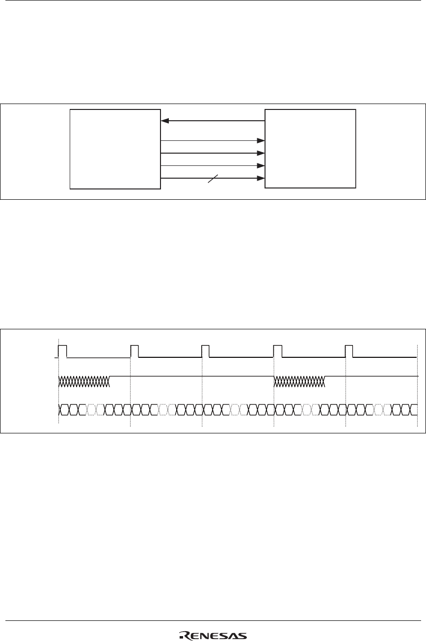
R61509V Target Spec
Rev. 0.11 April 25, 2008, page 116 of 181
FMARK Interface
In the FMARK interface operation, data is written to internal RAM via system interface synchronizing with
the frame mark signal (FMARK), realizing tearing less video image while using conventional system
interface. FMARK output position is set in units of line using FMP bit. Set the bit considering data transfer
speed.
RS
WRX
16
R61509V
FMARK
CSX
DB17-10, 8-1
HOST
PROCESSOR
Figure 38 FMARK Interface
In this operation, moving picture display is enabled via system interface by writing data at higher than the
internal display operation frequency to a certain degree, which guarantees rewriting the moving picture
RAM area without causing flicker on the display.
The data is written in the internal RAM. Therefore, when moving picture is displayed, data is written only
to the moving picture display area without using RGB or VSYNC interface, minimizing number of data
transfer required for moving picture display.
㩷
㩷
㩷
㩷
㩷
㩷
㩷
㩷
㩷
RAM data
write via
system interface
Display operation
synchronized with
internal clock
FMARK
Figure 39 Moving Picture Data Transfers via FMARK Function

R61509V Target Spec
Rev. 0.11 April 25, 2008, page 117 of 181
When transferring data in synchronization with FMARK signal, minimum RAM data write speed and
internal clock frequency must be taken into consideration. They must be more than the values calculated
from the following equations.
iancevar)clocks(23))BP(BackPorch)FP(FrontPorch)NL(esDisplayLin(encyFrameFrequ
) [Hz] ency (fosclock frequInternal c
××++×=
fosc
1
)clocks(16)insargm)NL(esDisplayLin)BP(BackPorch)FP(FrontPorch(
)NL(esDisplayLin240
]Hz.)[(mineedRAMWriteSp
××−++
×
>
Note: When RAM write operation is not started immediately following the rising edge of FMARK, the
time from the rising edge of FMARK until the start of RAM write operation must also be taken into
account.
Examples of calculating minimum RAM data write speed and internal clock frequency is as follows.
[Example]
Panel size 240 RGB
× 432 lines (NL = 6’h35: 432 lines)
Total number of lines (NL) 432 lines
Back/front porch 14/2 lines (BP = 4h’E, FP = 4’h2)
Frame marker position (FMP) Display end line: 432nd line (FMP = 9’h1BF)
Frame frequency 60 Hz
Internal oscillation frequency 678kHz
Internal oscillation frequency (fosc) [Hz] = 678kHz × 1.07 / 1.0 = 726 kHz (variance is taken into account)
Notes: 1.When setting the internal clock frequency, possible causes of fluctuation must also be taken into
consideration. In this example, the internal clock frequency allows for a margin of ±7% for
variances and guarantee that display operation is completed within one FMARK cycle.
2.This example includes variances attributed to LSI fabrication process and room temperature.
Other possible causes of variances, such as differences in external resistors and voltage change
are not considered in this example. It is necessary to include a margin for these factors.
Minimum speed for RAM writing [Hz]
> 240 × 320 / {((2+14 + 320 – 2) lines × 16 clocks) × 1/726 kHz} = 7.4 MHz
Notes: 1. In this example, it is assumed that the R61509V starts writing data in the internal RAM on the
rising edge of FMARK.
2.There must be at least a margin of 2 lines between the line to which the R61509V has just written
data and the line where display operation on the LCD is performed.
3.The FMARK signal output position is set to the line specified by FMP[8:0] bits.
In this example, RAM write operation at a speed of 7.4MHz or more, when starting on the rising edge of
FMARK, guarantees the completion of data write operation in a certain line address before the R61509V
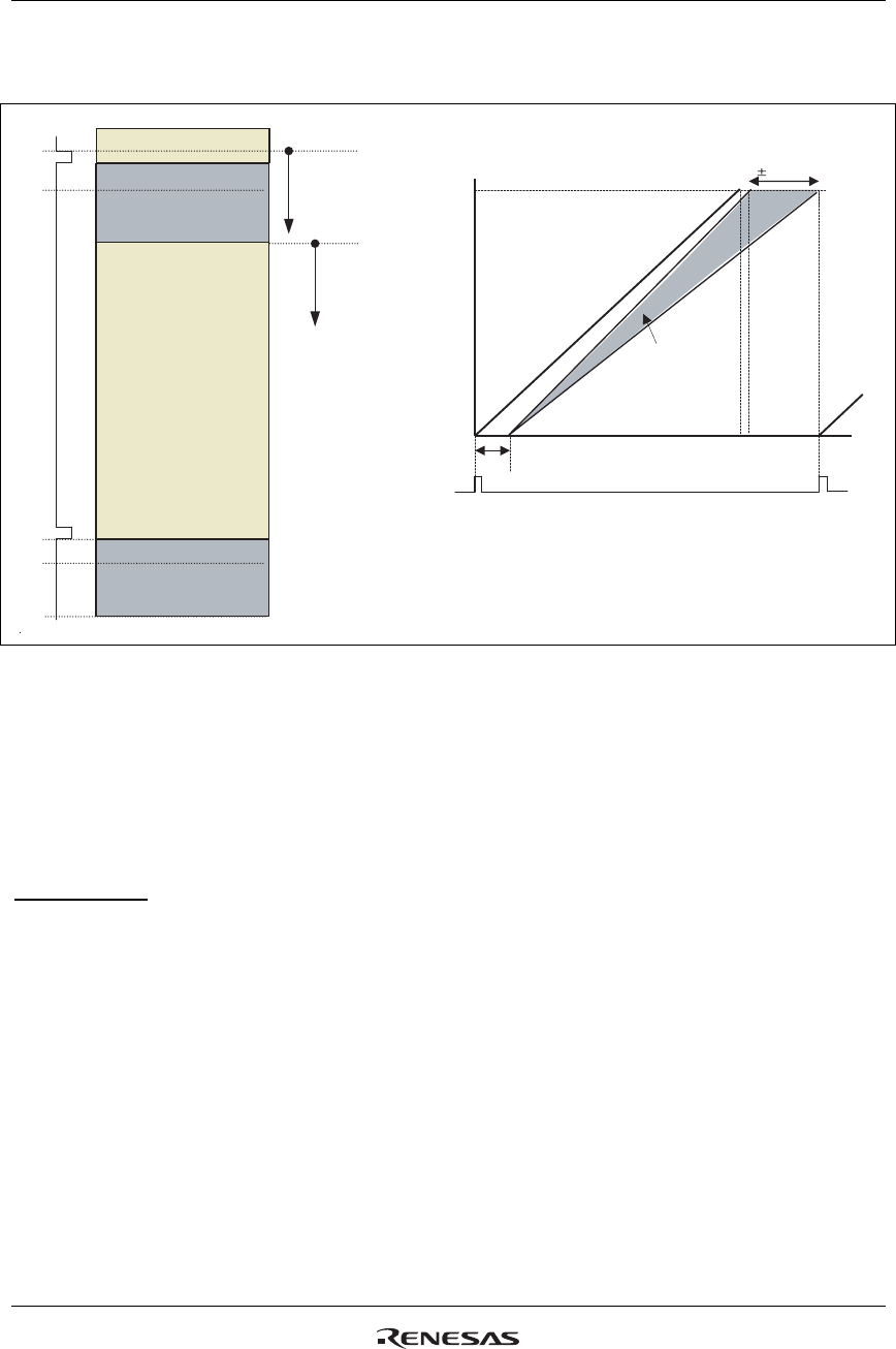
R61509V Target Spec
Rev. 0.11 April 25, 2008, page 118 of 181
starts the display operation of the data written in that line and can write moving picture data without
causing flicker on the display.
7%
FP+BP=16H
432
0
FMARK
16.67
(60Hz)
[ms]
FMARK
RAM
write
Display
operation
Back porch (14 lines)
Main panel
Moving picture
display
(432 lines)
Front porch (2 lines)
RC oscillation
Display
operation
[line]
RAM write
7.4MHz
Line processing
Back porch (14 lines)
Front porch (2 lines)
Figure 40
Note to display operation synchronous data transfer using FMARK signal
The above example of calculation gives a theoretical value. Possible causes of variances of internal
oscillator should be taken into consideration. Make enough margin in setting RAM write speed for
this operation.
FMP bit setting
The microcomputer detects FMARK signal outputted at the position defined by FMP bit. The R61509V
outputs an FMARK pulse when the R61509V is driving the line specified by FMP bits. The FMARK
signal can be used as a trigger signal to write display data in synchronization with display operation by
detecting the address where data is read out for display operation.
The FMARK output interval is set by FMI bits. Set FMI bits in accordance with display data rewrite cycle
and data transfer rate.
R61509V Target Spec
Rev. 0.11 April 25, 2008, page 119 of 181
Table 60 Table 61
FMP[8:0] FMARK output position
9’h000 0
9’h001 1st line
9’h002 2nd line
:
9’h1BD 445th line
9’h1BE 446th line
9’h1BF 447th line
9’h1C0 ~ 1FF Setting disabled
FMI[2] FMI[1] FMI[0] FMARK Output interval
0 0 0 One frame period
0 0 1 2 frame periods
0 1 1 4 frame periods
1 0 1 6 frame periods
Other setting Setting disabled
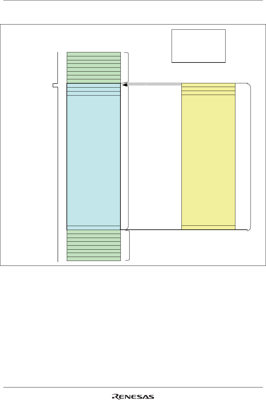
R61509V Target Spec
Rev. 0.11 April 25, 2008, page 120 of 181
FMP Setting Example
NL=6'h35
Front porch
Display area
FMP=9’h008
NL=6’h35 (432 lines)
FP=4’h8
BP=4’h8
VL=8’h00
Line address
Back porch
FMARK output position
FMP=9’h008
RAM physical line address
Base image
0 (1st line)
1 (2nd line)
2 (3rd line)
3 (4th line)
4 (5th line)
5 (6th line)
6 (7th line)
7 (8th line)
8 (1st line)
9 (2nd line)
10 (3rd line)
439 (432nd line)
440 (1st line)
441 (2nd line)
442 (3rd line)
443 (4th line)
444 (5th line)
445 (6th line)
446 (7th line)
447 (8th line)
AD[16:8]=9’h13F
AD[16:8]=9’h002
AD[16:8]=9’h000
AD[16:8]=9’h001
Figure 41
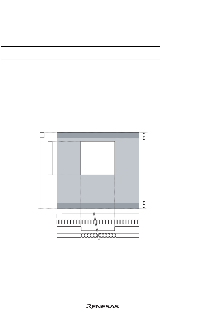
R61509V Target Spec
Rev. 0.11 April 25, 2008, page 121 of 181
RGB Interface
The R61509V supports the RGB interface. The interface format is set by RM[1:0] bits. The internal RAM
is accessible via RGB interface.
Table 62 RGB interface
RIM RGB Interface DB Pin
0 18-bit RGB interface DB17-0
1 16-bit RGB interface DB17-13, DB11-1
Note: Using multiple interface at a time is prohibited.
RGB Interface
The display operation via RGB interface is synchronized with VSYNCX, HSYNCX, and DOTCLK. The
data can be written only within the specified area with low power consumption by using window address
function. In RGB interface operation, front and back porch periods must be made before and after the
display period. When RGB interface is used, instructions should be transferred via clock synchronous serial
interface. RGB and 80-system bus interfaces cannot be used simultaneously.
VSYNCX
1. The front porch period continues until next VSYNCX input is detected.
2. Make sure to match the VSYNCX, HSYNCX, and DOTCLK frequencies to the resolution of liquid crystal panel.
Moving picture
display area
Display period (NL)
Back porch period (BP)
Front porch period (FP)
Notes:
Back porch period (BPP):
Front porch period (FPP):
Display period:
The number of lines for one frame:
14H ҈ BP ҈ 2H
14H ҈ FP ҈ 2H
FP + BP ҇ 16H
NL ҇ 432H
FP + NL + BP
VSYNCX: Frame synchronization signal
HSYNCX: Line synchronization signal
DOTCLK: Dot clock
ENABLE: Data enable signal
DB 17-0: RGB (6:6:6) display data
HSYNCX
DOTCLK
ENABLE (H)
DB17-0
ENABLE (V)
Figure 42 Display Operation via RGB Interface
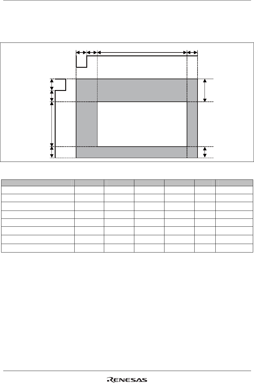
R61509V Target Spec
Rev. 0.11 April 25, 2008, page 122 of 181
Polarities of VSYNCX, HSYNCX, ENABLE, and DOTCLK Signals
The polarities of VSYNCX, HSYNCX, ENABLE, and DOTCLK signals can be changed by setting the
DPL, EPL, HSPL, and VSPL bits, respectively for convenience of system configuration.
㪧㪝㪟㫉㪻㪘㪟㪧㪙㪟㪺㫅㫐㫊㪟
㪭㫊㫐㫅㪺
㪙㪧
㪭㪙㪧
㪭㪘㪻㫉
㪭㪝㪧 㪝㪧
Valid data period
Figure 43
Table 63
Parameters Symbols Min. Typ. Max. Step Unit
Horizontal Synchronization Hsync 2 10 16 1 DOTCLKCYC
Horizontal Back Porch HBP 2 20 24 1 DOTCLKCYC
Horizontal Address HAdr - 240 - 1 DOTCLKCYC
Horizontal Front Porch HFP 2 10 16 1 DOTCLKCYC
Vertical Synchronization Vsync 1 2 4 1 Line
Vertical Back Porch VBP 1 2 - 1 Line
Vertical Address VAdr - 432 - 1 Line
Vertical Front Porch VFP 3 4 - 1 Line
Note: The values of typ. are based on the following conditions; the panel resolution is QVGA (240 ×
432), the clock frequency is 7.39MHz, and the frame frequency is about 60Hz.)
Vsync + VBP = BP. VFP = FP. Vadr = NL.
(Number of clocks per 1H) ≥ (Number of RTN clocks) × (1/1 div.) × (PCDIVL + PCDIVH)
The setting example is shown in the following page.
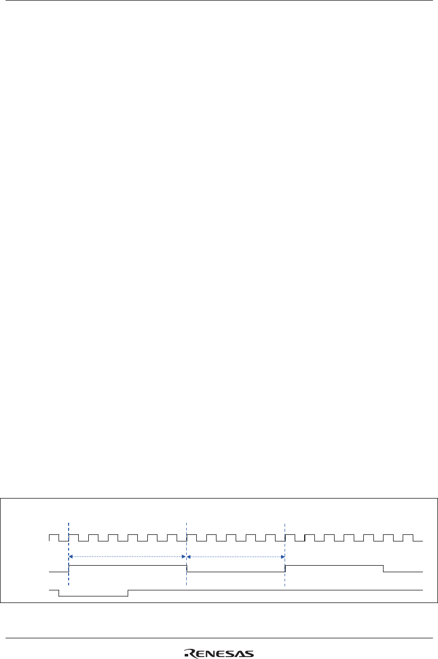
R61509V Target Spec
Rev. 0.11 April 25, 2008, page 123 of 181
Setting Example of Display Control Clock in RGB Interface Operation
Register
The display operation via DPI is performed in synchronization with the internal clock (PCLKD) that is
generated by dividing PCLK frequency.
PCDIVH[3:0]: When PCLKD is High, the number of clocks is set in unit of 1 clock.
PCDIVL[3:0]: When PCLKD is Low, the number of clocks is set in unit of 1 clock.
PCDIVH and PCDIVL (division ratio setting registers) should be set so that the difference between
PCLKD frequency and the internal oscillation clock (678kHz) is minimized.
Set PCDIVL to PCDIVH or PCDIVH − 1.
Make sure (number of PCLK frequency) ≥ (number of RTN clocks) ∗ (division ratio of DIV) ∗ (PCDIVH +
PCDIVL)
Setting example (frame frequency: 60Hz)
Internal clock: Internal oscillation clock = 678kHz
1/1 Div. = (DIVE[2:0] = 2’b0)
HFP = 10 clocks
FP = 8’h8, BP = 8’h8, NL = 6B (432 lines)
Æ 59.35Hz
PCLK: Hsync
= 10 clocks
HBP = 20 clocks
HFP = 10 clocks
60Hz × (8+432+8) lines (10+20+240+10) clocks = 7.53MHz
PCLK frequency = 7.53MHz
7.53MHz/678kHz
= 11.11 (Set PCDIVH and PCDIVL so that PCLK frequency is divided into
11.)
7.53/11 = 685kHz
685kHz / 25 clocks / 448 lines = 61.2Hz
PCDIVH = 4’h6
PCDIVL = 4’h5
㪧㪚㪛㪠㪭㪟㪔㪋㩾㪿㪍
㪧㪚㪛㪠㪭㪣㪔㪋㩾㪿㪌
㪧㪚㪣㪢
㪣㪭㪠㪛㪚㪧㪟㪭㪠㪛㪚㪧
㪧㪚㪣㪢㪛
㪟㪪㪰㪥㪚
Internal clock
Figure 44
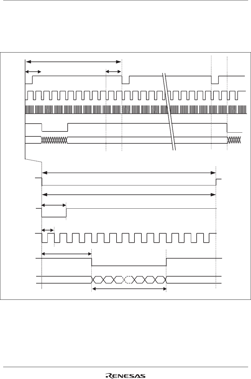
R61509V Target Spec
Rev. 0.11 April 25, 2008, page 124 of 181
RGB Interface Timing
The timing relationship of signals in RGB interface operation is as follows.
16-/18-Bit RGB Interface Timing
1H
1 clock
1H or more
One frame
Back porch period Front porch period
HLW ҈ 1CLK
DTST ҈ 1CLK
VSYNCX
HSYNCX
DOTCLK
ENABLE
DB17-0
VSYNCX
HSYNCX
DOTCLK
ENABLE
DB17-0
Valid data
Figure 45
Note: VLW: VSYNCX Low period
HLW: HSYNCX Low period
DTST: data transfer setup time
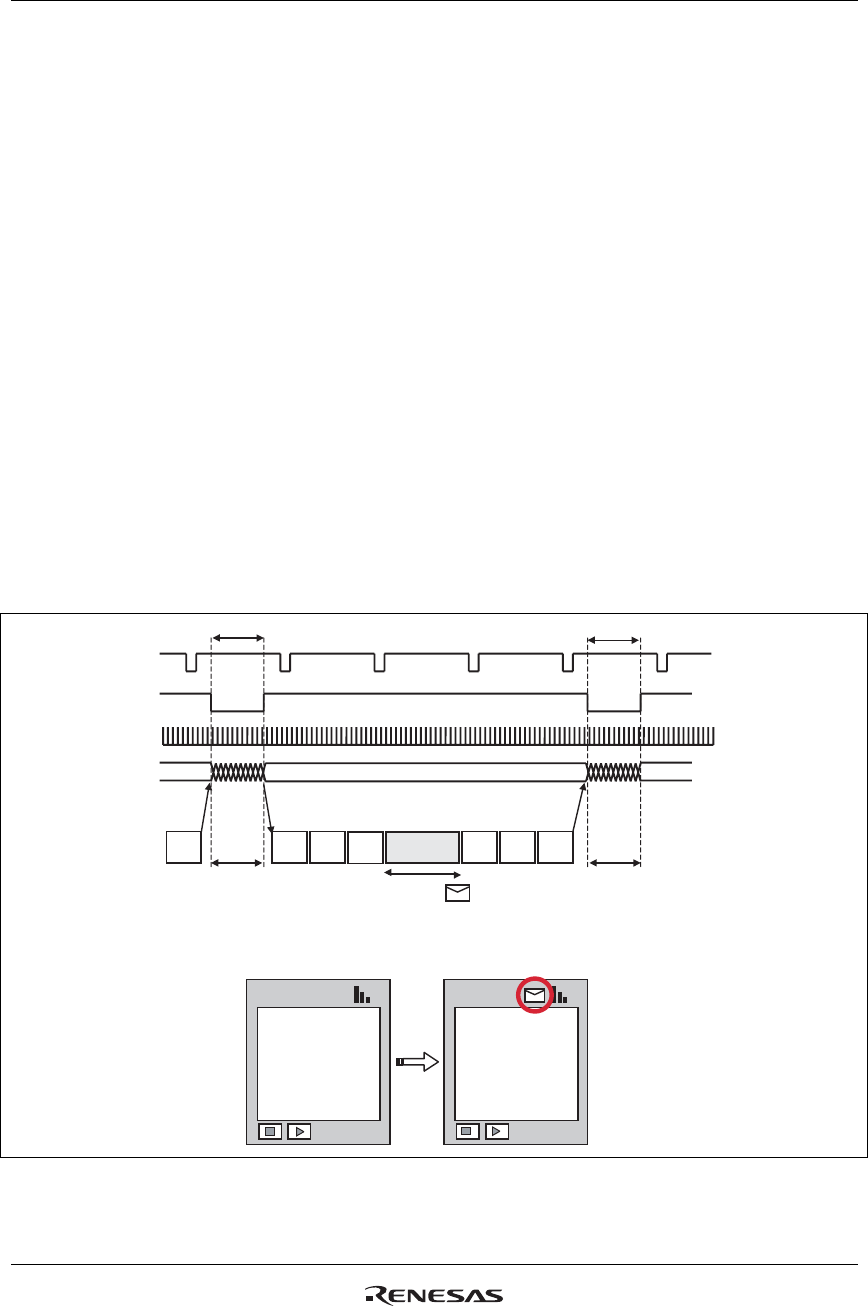
R61509V Target Spec
Rev. 0.11 April 25, 2008, page 125 of 181
Moving Picture Display via RGB Interface
The R61509V supports RGB interface for moving picture display and incorporates RAM for storing
display data, which provides the following advantages in displaying a moving picture.
1. The window address function enables transferring data only within the moving picture area
2. It becomes possible to transfer only the data written over the moving picture area
3. By reducing data transfer, it can contribute to lowering the power consumption of the whole system
4. The data in still picture area (icons etc.) can be written over via system interface while displaying a
moving picture via RGB interface
RAM access via system interface in RGB interface operation
The R61509V allows RAM access via system interface in RGB interface operation. In RGB interface
operation, data is written to the internal RAM in synchronization with DOTCLK while ENABLE is “Low”.
When writing data to the RAM via system interface, set ENABLE “High” to stop writing data via RGB
interface. Then set RM = “0” to enable RAM access via system interface. When reverting to the RGB
interface operation, wait for the read/write bus cycle time. Then, set RM = “1” and the index register to
R22h to start accessing RAM via RGB interface. If there is a conflict between RAM accesses via two
interfaces, there is no guarantee that the data is written in the RAM.
The following is an example of rewriting still picture data via system interface while displaying a moving
picture via RGB interface.
Update data in the
area other than
moving picture area
6/2
6/25
00:
00:
00
00
6/2
6/25
00:
00:
00
00
writing
still picture area
updating frame data updating frame data
VSYNCX
ENABLE
DOTCLK
DB17-0
System
interface
Note 3)
Note 3)
Moving picture
area
Moving picture
area
RAM
address
set
RM = 0
RAM
address
set
Index
R22
Index
R22
Index
R22
writing
moving picture area
writing
moving picture area
RM = 1
Notes:
1. In RGB interface operation, RAM address AD16-0 is set in the address counter on the falling edge of VSYNCX.
2. Set AD16-0 bits and the index R22h before starting RAM access via RGB interface.
3. When switching to the system interface operation after writing data via RGB interface, wait at least one write cycle (tcycw).
Figure 46 Updating the Still Picture Area while Displaying Moving Picture
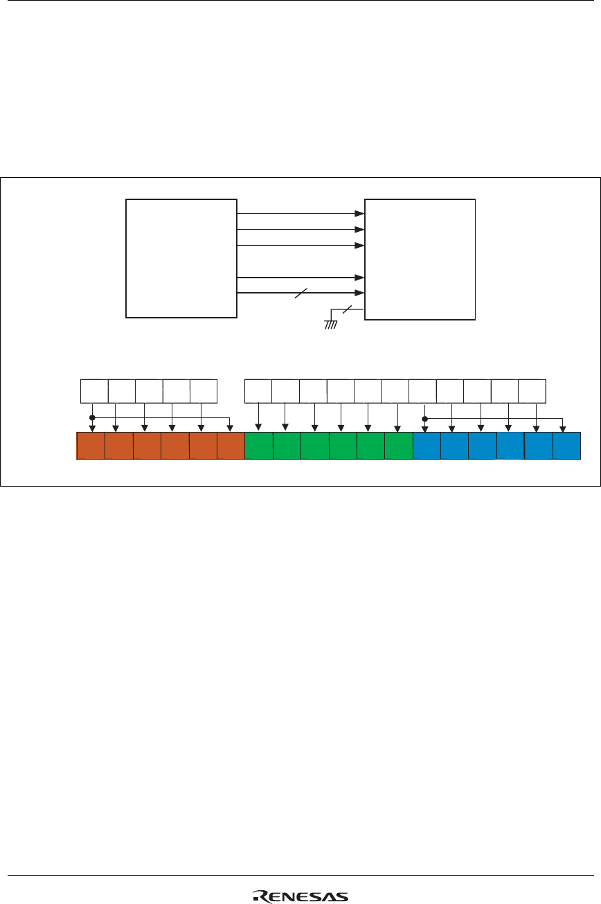
R61509V Target Spec
Rev. 0.11 April 25, 2008, page 126 of 181
16-Bit RGB Interface
The 16-bit RGB interface is selected by setting RIM = 1. The display operation is synchronized with
VSYNCX, HSYNCX, and DOTCLK signals. The display data is transferred to the internal RAM in
synchronization with the display operation via 16-bit ports while data enable signal (ENABLE) allows
RAM access via RGB interface.
Instruction bits can be transferred only via system interface.
HOST
PROCESSOR
16
2
Input
DB
17
DB
16
DB
15
DB
14
DB
13
DB
11
DB
10
DB
9
DB
8
DB
7
DB
6
DB
5
DB
4
DB
3
DB
2
DB
1
DB17-13, 11-1
DB12,0
VSYNCX
HSYNCX
DOTCLK
ENABLE
R61509V
RIM = 1
Data format for the16-bit interface (RIM = 1)
R5 R4 R3 R2 R1 R0 G5 G4 G3 G2 G1 G0 B5 B4 B3 B2 B1 B0
Note: 65,536-color display1 pixel
GRAM data
Figure 47 Example of 16-Bit RGB Interface and Data Format
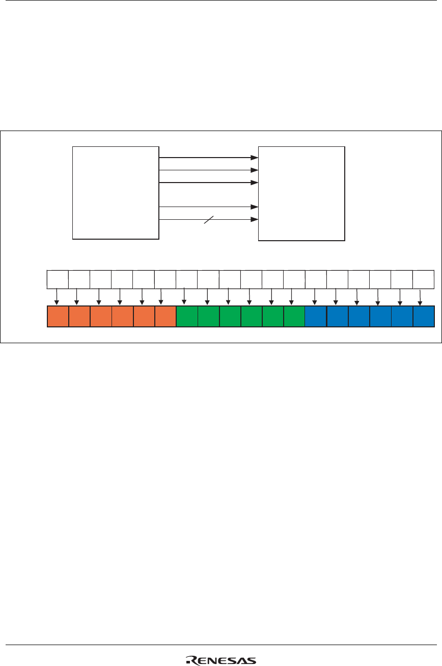
R61509V Target Spec
Rev. 0.11 April 25, 2008, page 127 of 181
18-bit RGB Interface
The 18-bit RGB interface is selected by setting RIM = 0. The display operation is synchronized with
VSYNCX, HSYNCX, and DOTCLK signals. The display data is transferred to the internal RAM in
synchronization with the display operation via 18-bit ports (DB17-0) while data enable signal (ENABLE)
allows RAM access via RGB interface.
Instruction bits can be transferred only via system interface.
HOST
PROCESSOR R61509V
18
DOTCLK
ENABLE
DB17-0
DB
17
DB
16
DB
15
DB
14
DB
13
DB
12
DB
11
DB
10
DB
9
DB
8
DB
7
DB
6
DB
5
DB
4
DB
3
DB
2
DB
1
DB
0
RIM = 0
Data format for the 18-bit interface (RIM = 0)
Input
GRAM write
data
1 pixel Note: Normal display in 262,144 colors
R5 R4 R3 R2 R1 R0 G5 G4 G3 G2 G1 G0 B5 B4 B3 B2 B1 B0
VSYNCX
HSYNCX
Figure 48 Example of 18-Bit RGB Interface and Data Format
R61509V Target Spec
Rev. 0.11 April 25, 2008, page 128 of 181
Notes to RGB Interface Operation
1. The following functions are not available in RGB interface operation.
Table 64 Functions Not Available in RGB Interface operation
Function RGB Interface Internal Display Operation
Partial display Not available Available
Scroll function Not available Available
2. The VSYNCX, HSYNCX, and DOTCLK signals must be supplied during display period.
3. The reference clock to generate liquid crystal panel controlling signals in RGB interface operation is
DOTCLK, not the internal clock generated from the internal oscillator.
4. When switching between the internal operation mode and the external display interface operation mode,
follow the sequences below in setting instruction.
5. In RGB interface operation, front porch period continues after the end of frame period until next
VSYNCX input is detected.
6. RGB and 80-system bus interfaces cannot be used simultaneously.
7. In RGB interface operation, RAM address AD16-0 is set in the address counter every frame on the
falling edge of VSYNCX.
Internal Clock Operation to RGB Interface (1)
Operation via RGB interface
RGB Interface (1) to Internal Clock Operation
Internal clock operation
AM = 0
RAM address set
Set DM1-0 = 01 and RM = 1
for RGB interface
Write data to RAM
via RGB interface
Wait one frame period
or more
Set index register to R202h
Display operation in
synchronization with
internal clocks
RGB interface operation Display operation in
synchronization with
VSYNCX, HSYNCX, and
DOTCLK
Display operation in
synchronization with VSYNCX,
HSYNCX, and DOTCLK
Internal clock operation
Set internal clock
operation mode*
(DM1-0 = 00 and RM = 0)
Display operation in
synchronization with
internal clocks
Note: Continue RGB interface signals at least for
one frame period after setting DM1-0, RM bits
to internal clock operation.
Note: Input the RGB interface signals before setting the DM1-0 and RM bits
to the RGB interface operation.
*Instruction setting for
the RGB interface operation
is enebled from the next frame period.
*Instruction setting to the
internal clock operation
is enebled from the next
frame period.
Wait one frame period
or more
Figure 49 RGB and Internal Clock Operation Mode Switching Sequences
R61509V Target Spec
Rev. 0.11 April 25, 2008, page 129 of 181
RAM Address and Display Position on the Panel
The R61509V has memory to store display data of 240RGB x 432 lines. The R61509V incorporates a
circuit to control partial display, which allows switching driving method between full-screen display mode
and partial display mode.
The R61509V makes display arrangement setting and panel driving position control setting separately and
specifies RAM area for each image displayed on the panel.
The following is the sequence of setting full-screen and partial display.
1. Set (PTSA, PTEA) to specify the RAM area for each partial image
2. Set the display position of each partial image on the base image by setting PTDP.
3. Set NL to specify the number of lines to drive the liquid crystal panel to display the base
image
4. After display ON, set display enable bits (BASEE, PTDE) to display respective images
Normal display BASEE = 1, PTDE = 0
Partial display BASEE = 0, PTDE = 1
5. Changes BASEE, PTDE settings when turning on and off the full and partial displays 1/2.
In driving the liquid crystal panel, the clock signal for gate line scan is supplied consecutively via interface
in accordance with the number of lines to drive the liquid crystal panel (NL setting).
When switching the display position in horizontal direction, set SS bit when writing RAM data.
Table 65
Display ENABLE Numbers of lines RAM area
Base image BASEE NL (VSA, VEA)
Note: The base image is displayed from the first line of the screen.
Table 66
Display ENABLE Display position RAM area
Partial image PTDE PTDP (PTSA, PTEA)
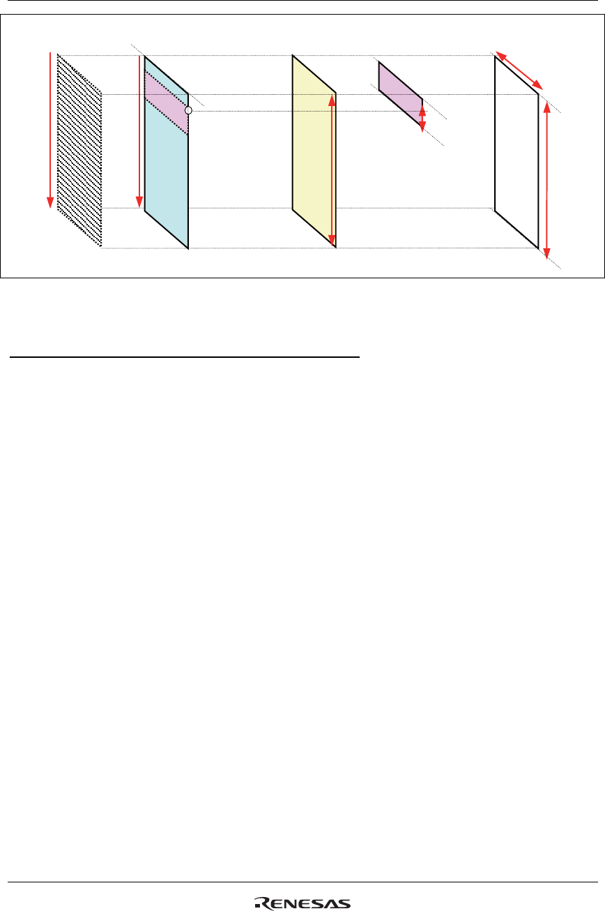
R61509V Target Spec
Rev. 0.11 April 25, 2008, page 130 of 181
(VSA,VEA)
9’h000
9’h1AF
NL
(HSA,HEA)
Window
Address
PTDP
1
PTSA0
PTEA0
䇼LCD䇽
Panel display
position
Display data
output position
Base image
RAM address Partial image
RAM address
RAM write
address
Partial
image
Base
image
Scan
direction
Figure 50 RAM Address, Display Position and Drive Position
Restrictions in Setting Display Control Instruction
There are restrictions in coordinates setting for display data, display position and partial display.
Screen setting
In setting the number of lines to drive the liquid crystal panel, make sure that the total number of lines is
432 lines or less (NL ≤ 432 lines).
Base image display
The base image is displayed from the first line of the screen: Base image display start position = 1st line
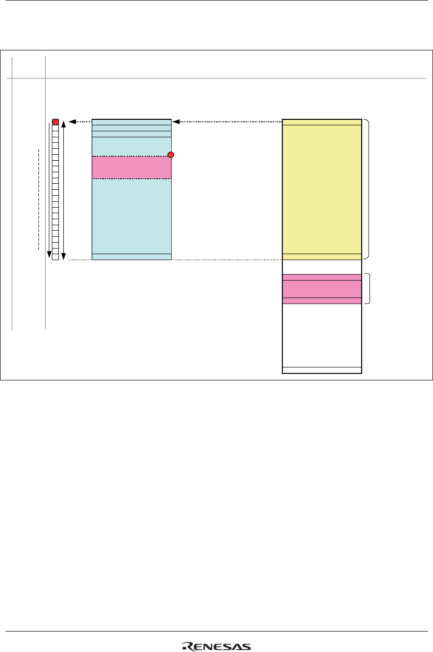
R61509V Target Spec
Rev. 0.11 April 25, 2008, page 131 of 181
The following figure shows the relationship among the RAM address, display position, and the lines driven
for the display.
0
3
NL
9’h000
n-1
(
n line
)
NL
PTDP
1
PTSA
PTEA
9’h1AF
1
2
4
5
NL
Base image
RAM area
Partial image
RAM area
Partial image
Display area
LCD panel
physical line address
RAM line address
Display
data output
order
Display screen
0 (1st line)
1 (2nd line)
2 (3rd line)
Figure 51 Display RAM Address and Panel Display Position
Note: This figure shows the relationship between RAM line address and the display position on the panel.
In the R61509V’s internal operation, the data is written in the RAM area specified by the window
address setting.
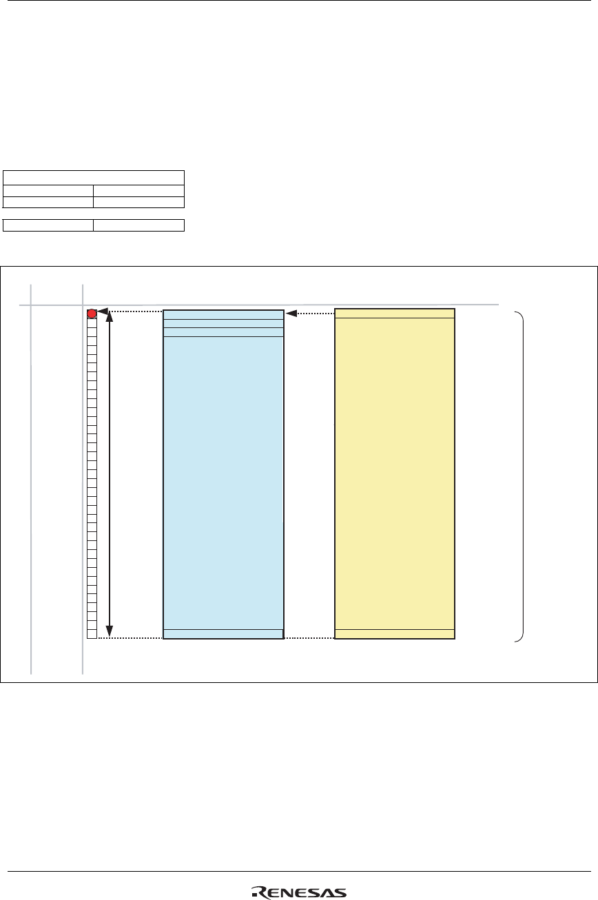
R61509V Target Spec
Rev. 0.11 April 25, 2008, page 132 of 181
Instruction Setting Example
The followings are examples of settings for 240(RGB) x 432(lines) panel.
1. Full screen display (no partial display)
The following is an example of settings for full screen display.
Table 67
Base image display instruction
BASEE 1
NL[5:0] 6’h35
PTDE 0
3
NL
(432 lines)
431 (432nd line)
1
2
4
5
432
9’h000
BSA=9'h000
BEA = 9’h1AF
LCD panel
physical line address
0 (1st line)
1 (2nd line)
2 (3rd line)
RAM line address
Display
data output
order
BASE image
RAM area
Base image
Figure 52 Full Screen Display (no Partial)
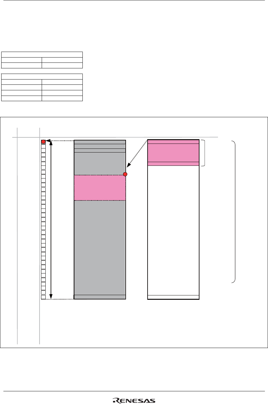
R61509V Target Spec
Rev. 0.11 April 25, 2008, page 133 of 181
2. Partial only
The following is an example of settings for displaying partial image 1 only and turning off the base image.
The partial image 1 is displayed at the position specified by PTDP0 bit.
Table 68
Base image display instruction
BASEE 0
NL[5:0] 6’h35
partial image 1 display instruction
PTDE 1
PTSA[8:0] 9’h000
PTEA[8:0] 9’h00F
PTDP[8:0] 9’h080
3
1
2
4
5
432 9’h1AF
PTSA=9’000
PTEA=9’00F
PTDP
Display
data output
order RAM line address
LCD panel
physical line address
Partial image
display area
Base image
(non-lit display)
Partial image
RAM area
Base image
RAM area
NL
(432 linrs)
0 (1st line)
1 (2nd line)
2 (3rd line)
431 (432nd line)
Figure 53 Partial Display
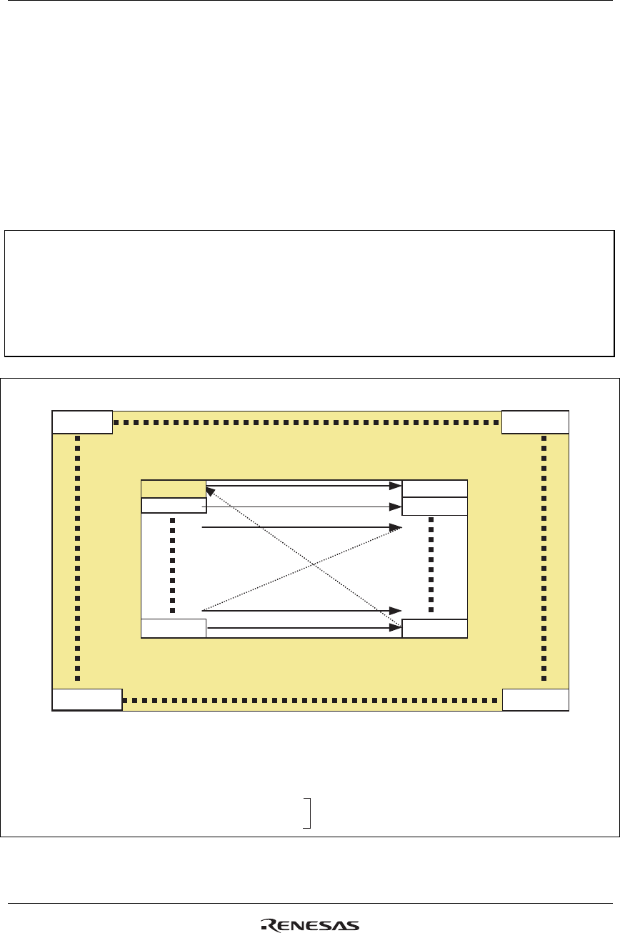
R61509V Target Spec
Rev. 0.11 April 25, 2008, page 134 of 181
Window Address Function
The window address function enables writing display data consecutively in a rectangular area (a window
address area) made in the internal RAM. The window address area is described by the horizontal address
register (start: HSA7-0, end: HEA7-0 bits) and the vertical address register (start: VSA8-0, end: VEA8-0
bits). The AM and ID bits set the transition direction of RAM address (either increment or decrement,
horizontal or vertical, respectively). Setting these bits enables the R61509V to write data including image
data consecutively without taking the data wrap position into account.
The window address area must be made within the GRAM address map area. Also, the AD16-0 bits (RAM
address set register) must be set to an address within the window address area.
[Window address area setting range]
(Horizontal direction) 8’h00 ≤ HSA ≤ HEA ≤ 8’hEF
(Vertical direction) 9’h000 ≤ VSA ≤ VEA ≤ 9’h1AF
[RAM Address setting range]
(RAM address) HSA ≤ AD7-0 ≤ HEA
VSA ≤ AD16-8 ≤ VEA
Window address area
GRAM address map
17'h00000 17'h000EF
17'h1AF00 17'h1AFEF
17'h02010
17'h02110
17'h05F10
17'h0212F
17'h0202F
17'h05F2F
ORG = 0 RAM address set = 17'02010 (arbitrary)
ORG = 1 RAM address set = 17'00000
Both are set to the same RAM address.
HSA = 8'h10, HEA = 8'h2F ID = 2'h3 (increment)
VSA = 9'h020, VEA = 9'h05F AM = 1'h0 (horizontal writing)
Window address area
Figure 54 Automatic Address Update within a Window Address Area
R61509V Target Spec
Rev. 0.11 April 25, 2008, page 135 of 181
Scan Mode Setting
The R61509V can set the gate pin assignment and the scan direction in the following 4 different ways by
setting SM and GS bits to realize various connections between the R61509V and the LCD panel.
SM Scan direction
0
Note: the numbers in the circles in the figure shows the order of scan.
G1ЈG2ЈG3ЈG4.... G429ЈG430ЈG431ЈG432
R61509V
432
430
2
main
Panel
176
431
429
1
(Non-bump view)
240
Interchanging forward direction (GS=0)
34
G4ЈG3ЈG2ЈG1....G432ЈG431ЈG430ЈG3429
R61509V
main
Panel
176
2
4
(Non-bump view)
240
432
Interchanging backward direction (GS=1)
432
430
Scan order (Gate line No.)
G4ЈG2ЈG431ЈG429 ....
G3ЈG1
G432ЈG430 ....
R61509V
1
2
216
main
Panel
(Non-bump view)
240
432
Left/right backward direction (GS=1)
215
217
218
432
431
1
Scan order (Gate line No.)
G2ЈG4....G1ЈG3.... G429ЈG431Ј
G430ЈG432
R61509V
432
431
217
main
Panel
(Non-bump view)
240
432
Left/right forward direction (GS=0)
218
216
215
1
2
Scan order (Gate line No.)
Scan order (Gate line No.)
1
3
431
429
(GS) (GS)
(GS)
(GS)
Figure 55
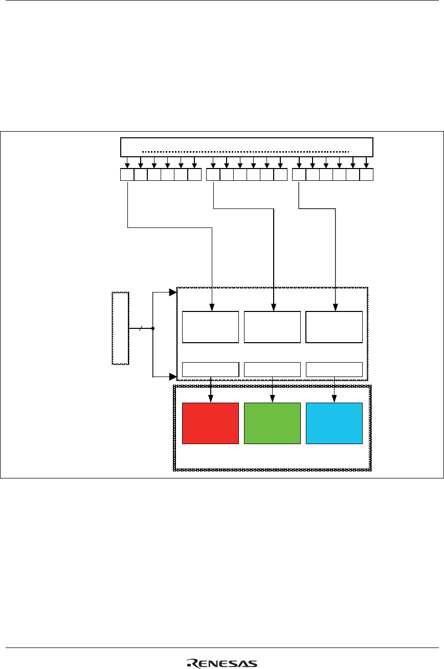
R61509V Target Spec
Rev. 0.11 April 25, 2008, page 136 of 181
8-Color Display Mode
The R61509V has a function to display in eight colors. In this display mode, only V0 and V63 are used
and power supplies to other grayscales (V1 to V62) are turned off to reduce power consumption.
In 8-color display mode, the γ-adjustment registers R300 to R309 are disabled and the power supplies to V1
to V62 are halted. The R61509V does not require GRAM data rewrite for 8-color display by writing the
MSB to the rest in each dot data to display in 8 colors.
2
R G B
LCD
V63
V0
B5
G5R5
R5R4R3R2R1R0G5G4G3G2G1G0B5B4B3B2B1B0
BSLBSM
LCD driver LCD driver LCD driver
Display data
GRAM
2-level grayscale
control
<R>
2-level grayscale
control
2-level grayscale
control
<G> <B>
Grayscale amplifier
Figure 56 8-Color Display Mode

R61509V Target Spec
Rev. 0.11 April 25, 2008, page 137 of 181
Frame-Frequency Adjustment Function
The R61509V supports a function to adjust frame frequency. The frame frequency for driving liquid
crystal can be adjusted by setting the DIVI, RTNI bits without changing the oscillation frequency.
By changing the DIVI and RTNI settings, the R61509V can operate at high frame frequency when
displaying a moving picture, which requires the R61509V to rewrite data in high speed, and it can operate
at low frame frequency when displaying a still picture.
Relationship between Liquid Crystal Drive Duty and Frame Frequency
The following equation represent the relationship between liquid crystal drive duty and frame frequency.
The frame frequency can be changed by setting the 1H period adjustment bit (RTNI) and the operation
clock frequency division ratio setting bit (DIVI).
Equation for calculating frame frequency
][
)(/ Hz
BPFPLinetioDivisionRalineocksNumberofCl
fosc
encyFrameFrequ ++××
=
fosc: RC oscillation frequency
Number of clocks per line: RTNI bit
Division ratio: DIVI bit
Line: number of lines to drive the LCD panel (NL bit)
Number of lines for front porch: FP
Number of lines for back porch: BP
Example of Calculation: when maximum frame frequency = 60 Hz
fosc: 678 kHz
Number of lines: 432 lines
1H period: 25 clock cycles (RTNI [4:0] = “11001”)
Division ratio of operating clock: 1/1
Front porch: 2 lines
Back porch: 14 lines
f
FLM = 678 (kHz) / 25 (clocks) × 1/1 × (432+2+14) (lines) ≒ 60.5 (Hz)
R61509V Target Spec
Rev. 0.11 April 25, 2008, page 138 of 181
Under the above conditions, the frame frequency can be changed according to the table shown below.
Table 69 Frame Frequency Setting (NL = 432 lines, BP = 14 lines, FP = 2 lines, fosc = 678 kHz)
RTNI[4:0] DIVI = 2’h0 DIVI = 2’h1
5’h00 - 5’h0F - -
5’h10 95 Hz 47 Hz
5’h11 89 Hz 45 Hz
5’h12 84 Hz 42 Hz
5’h13 80 Hz 40 Hz
5’h14 76 Hz 38 Hz
5’h15 72 Hz 36 Hz
5’h16 69 Hz 34 Hz
5’h17 66 Hz 33 Hz
5’h18 63 Hz 32 Hz
5’h19 61 Hz 30 Hz
5’h1A 58 Hz 29 Hz
5’h1B 56 Hz 28 Hz
5’h1C 54 Hz 27 Hz
5’h1D 52 Hz 26 Hz
5’h1E 50 Hz 25 Hz
5’h1F 49 Hz 24 Hz
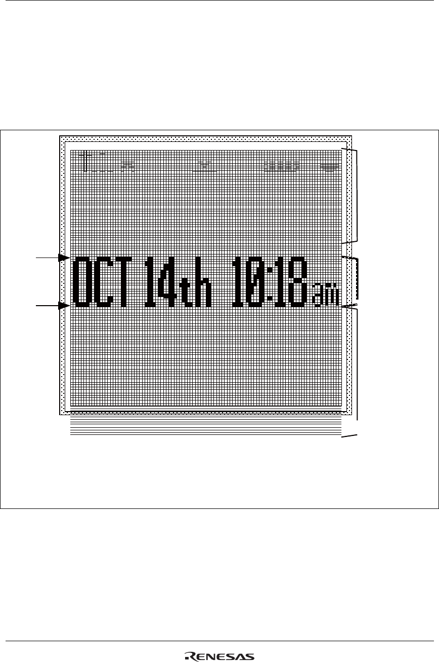
R61509V Target Spec
Rev. 0.11 April 25, 2008, page 139 of 181
Partial Display Function
The partial display function allows the R61509V to drive lines selectively to display partial images by
setting partial display control registers. The lines not used for displaying partial images are driven at non-
lit display level to reduce power consumption.
The power efficiency can be enhanced in combination with 8-color display mode. Check the display
quality when using low power consumption functions.
G41
G60
Non-lit display area
Non-lit display area
Partial image:
20 lines
Number of lines to drive LCD: NL = 6’h35 (432 lines)
Base image display enable: BASEE = 0
Partial image display RAM area: (PTSA, PTEA) = (9’h000, 9’h013)
Partial image display position: PTDP = 9’h028
Partial image display enable: PTDE = 1
Figure 57 Partial Display
Note: See the RAM Address and Display Position on the Panel for details on the relationship between the
display positions of partial images and respective RAM area setting.
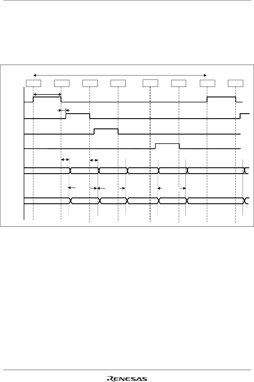
R61509V Target Spec
Rev. 0.11 April 25, 2008, page 140 of 181
Liquid Crystal Panel Interface Timing
The relationships between RGB interface signals and liquid crystal panel control signals in internal
operation and RGB interface operations are as follows.
Internal Clock Operation
FMAR
K
G1
G2
S
(
3n+1
)
VCOM
1H
(FMP=BP-1)
NOWI
432nd line
G432
R,G,B
S
(
3n+2
)
S
(
3n+3
)
n=0to239
R,G,B R,G,B
SDTI
SDTI
reference
point
reference
point
reference
point
reference
point
reference
point
reference
point
reference
point
reference
point
One Frame
First line Second line
Figure 58
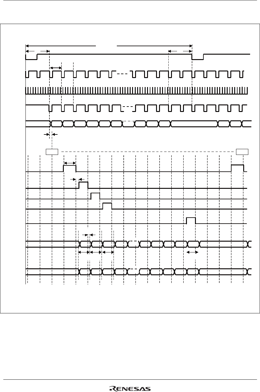
R61509V Target Spec
Rev. 0.11 April 25, 2008, page 141 of 181
RGB Interface Operation
1 2 3 4 5 6 432431430 1 2 3
BP
1H
5DOTCLK
FP
One frame
VSYNCX
HSYNCX
DOTCL
K
S
(
3n+1
)
ENABLE
DB
FMAR
K
G1
G2
G3
RGB 432 1
G432
VCOM
(FMP=BP-1)
1H
NOWE
S
(
3n+2
)
S
(
3n+3
)
n=0 to 239
RGB RGB
SDTE
Note: Transfer RGB data in one transfer via 16-bit port
See note
Reference
point
Reference
point
FIrst line
Second line
Third line 432nd line
Figure 59
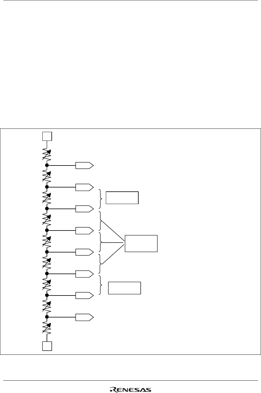
R61509V Target Spec
Rev. 0.11 April 25, 2008, page 142 of 181
γ Correction Function
γ Correction Function
The R61509V supports γ-correction function to make the optimal colors according to the characteristics of
the panel. The R61509V has registers for positive and negative polarities.
γ Correction Circuit
The following figure shows the γ-correction circuit. According to the settings of variable resistors R0 to R8,
the voltage level, the difference between VREG1OUT and VGS, is evenly divided into 8 grayscale
reference voltages (V0, V1, V8, V20, V43, V55, V62, and V63). Other 56-grayscale voltages are
generated by setting the level at a certain interval between the reference voltages. For grayscale voltage,
see “Grayscale Voltage Calculation Formula”.
㪭㪇
㪭㪈
㪭㪏
㪭㪉㪇
㪭㪋㪊
㪭㪌㪌
㪭㪍㪉
㪭㪍㪊
Linear
interpolation
Interpolation
adjustment
Interpolation
adjustment
R: Resistor outputting voltage evenly divided into 12
(1R): Trimming step
2~33R (1R)
1~32R (1R)
2~33R (1R)
4~19R (1R)
8~23R (1R)
0~31R (1R)
1~32R (1R)
2~33R (1R)
4~19R (1R)
VGS (=GND)
R0
R1
R2
R3
R4
R5
R6
R7
R8
VREG1OUT
Figure 60
R61509V Target Spec
Rev. 0.11 April 25, 2008, page 143 of 181
γ Correction Registers
The γ-correction registers include 42 bits for each of R, G, and B dots and 8-bit interpolation adjustment
registers.
Reference level adjustment registers
Table 70 Reference level adjustment registers
Gamma Control
Resistor Positive
polarity
Negative
polarity
R0 PR0P00[4:0] PR0N00[4:0]
R1 PR0P01[4:0] PR0N01[4:0]
R2 PR0P02[4:0] PR0N02[4:0]
R3 PR0P03[3:0] PR0N03[3:0]
R4 PR0P04[3:0] PR0N04[3:0]
R5 PR0P05[3:0] PR0N05[3:0]
R6 PR0P06[4:0] PR0N06[4:0]
R7 PR0P07[4:0] PR0N07[4:0]
R8 PR0P08[4:0] PR0N08[4:0]
R61509V Target Spec
Rev. 0.11 April 25, 2008, page 144 of 181
Table 71 Reference Level Adjustment Registers and Resistors
Register Register
Resistor Name Value Resistance Resistor Name Valie Resistance
5'h00 0R 4'h0 4R
5'h01 1R 4'h1 5R
5'h02 2R 4'h2 6R
R0 PR0*00[4:0]
5'h1F 31R
R5 PR0*05[3:0]
4'hF 19R
5'h00 1R 5'h00 2R
5'h01 2R 5'h01 3R
5'h02 3R 5'h02 4R
R1 PR0*01[4:0]
5'h1F 32R
R6 PR0*06[4:0]
5'h1F 33R
5'h00 2R 5'h00 1R
5'h01 3R 5'h01 2R
5'h02 4R 5'h02 3R
R2 PR0*02[4:0]
5'h1F 33R
R7 PR0*07[4:0]
5'h1F 32R
4'h0 4R 5'h00 2R
4'h1 5R 5'h01 3R
4'h2 6R 5'h02 4R
R3 PR0*03[3:0]
4'hF 19R
R8 PR0*08[4:0]
5'h1F 33R
4'h0 8R
4'h1 9R
4'h2 10R
R4 PR0*04[3:0]
4'hF 23R
Note: * indicates P / N.
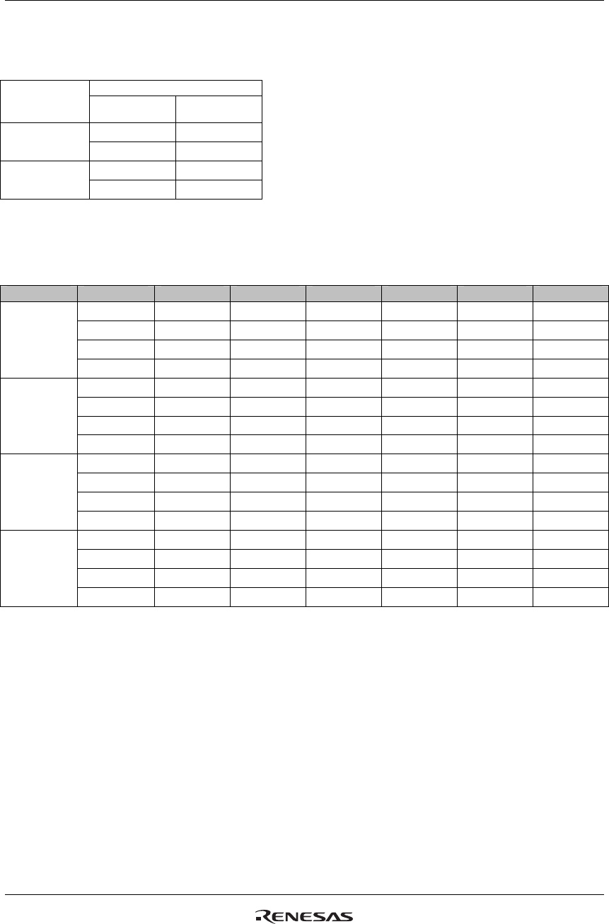
R61509V Target Spec
Rev. 0.11 April 25, 2008, page 145 of 181
Interpolation Registers
Table 72 Interpolation Registers
Gamma Control
Interpolation
adjustment Positive
polarity
Negative
polarity
PI0P0[1:0] PI0N0[1:0]
V2~V7 PI0P1[1:0] PI0N1[1:0]
PI0P2[1:0] PI0N2[1:0]
V56~V61 PI0P3[1:0] PI0N3[1:0]
Table 73 Interpolation factor for V2 to V7
(See “Grayscale Voltage Calculation Formula” for IPV* level)
PI0*0[1:0] PI0*1[1:0] IPV2 IPV3 IPV4 IPV5 IPV6 IPV7
2'h0 81% 67% 52% 39% 26% 13%
2'h1 78% 61% 43% 33% 22% 11%
2'h2 73% 52% 31% 23% 15% 8%
2'h0
2'h3 72% 50% 28% 21% 14% 7%
2'h0 80% 68% 56% 42% 28% 14%
2'h1 76% 62% 48% 36% 24% 12%
2'h2 70% 52% 35% 26% 17% 9%
2'h1
2'h3 69% 50% 31% 23% 16% 8%
2'h0 78% 70% 61% 46% 30% 15%
2'h1 74% 63% 53% 39% 26% 13%
2'h2 66% 53% 39% 29% 20% 10%
2'h2
2'h3 64% 50% 36% 27% 18% 9%
2'h0 78% 70% 63% 47% 31% 16%
2'h1 73% 64% 54% 41% 27% 14%
2'h2 65% 53% 41% 31% 20% 10%
2'h3
2'h3 63% 50% 37% 28% 19% 9%
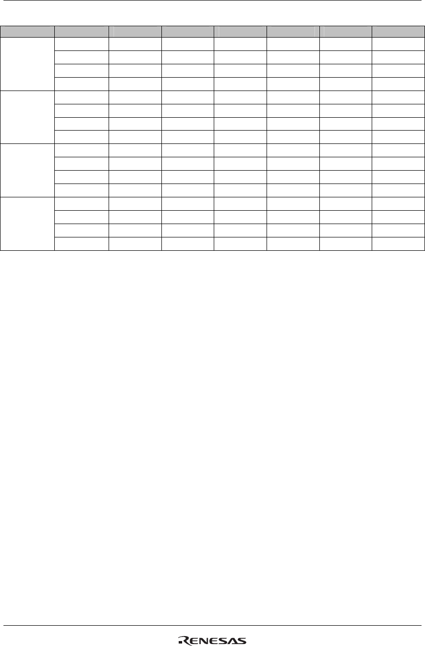
R61509V Target Spec
Rev. 0.11 April 25, 2008, page 146 of 181
Table 74 Interpolation Factor for V56 to V61
PI0*3[1:0] PI0*2[1:0] IPV56 IPV57 IPV58 IPV59 IPV60 IPV61
2'h0 87% 74% 61% 48% 33% 19%
2'h1 89% 78% 67% 57% 39% 22%
2'h2 92% 85% 77% 69% 48% 27%
2'h0
2'h3 93% 86% 79% 72% 50% 28%
2'h0 86% 72% 58% 44% 32% 20%
2'h1 88% 76% 64% 52% 38% 24%
2'h2 91% 83% 74% 65% 48% 30%
2'h1
2'h3 92% 84% 77% 69% 50% 31%
2'h0 85% 70% 54% 39% 30% 22%
2'h1 87% 74% 61% 47% 37% 26%
2'h2 90% 80% 71% 61% 47% 34%
2'h2
2'h3 91% 82% 73% 64% 50% 36%
2'h0 84% 69% 53% 38% 30% 22%
2'h1 86% 73% 59% 46% 36% 27%
2'h2 90% 80% 69% 59% 47% 35%
2'h3
2'h3 91% 81% 72% 63% 50% 37%
Note: * indicates P/N.
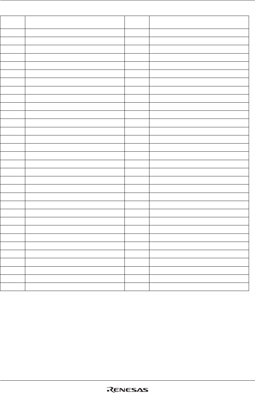
R61509V Target Spec
Rev. 0.11 April 25, 2008, page 147 of 181
Table 75 Grayscale Voltage Calculation Formula
Grayscale
voltage Formula Grayscale
voltage Formula
V0 ΔV x Σ(R1~R8)/SUMR V32 V43 + (V20 - V43) x 11/23
V1 ΔV x Σ(R2~R8)/SUMR V33 V43 + (V20 - V43) x 10/23
V2 V8 + (V1 - V8) x IPV2 V34 V43 + (V20 - V43) x 9/23
V3 V8 + (V1 - V8) x IPV3 V35 V43 + (V20 - V43) x 8/23
V4 V8 + (V1 - V8) x IPV4 V36 V43 + (V20 - V43) x 7/23
V5 V8 + (V1 - V8) x IPV5 V37 V43 + (V20 - V43) x 6/23
V6 V8 + (V1 - V8) x IPV6 V38 V43 + (V20 - V43) x 5/23
V7 V8 + (V1 - V8) x IPV7 V39 V43 + (V20 - V43) x 4/23
V8 ΔV x Σ(R3~R8)/SUMR V40 V43 + (V20 - V43) x 3/23
V9 V20 + (V8 - V20) x 11/12 V41 V43 + (V20 - V43) x 2/23
V10 V20 + (V8 - V20) x 10/12 V42 V43 + (V20 - V43) x 1/23
V11 V20 + (V8 - V20) x 9/12 V43 ΔV x Σ(R5~R8)/SUMR
V12 V20 + (V8 - V20) x 8/12 V44 V55 + (V43 - V55) x 11/12
V13 V20 + (V8 - V20) x 7/12 V45 V55 + (V43 - V55) x 10/12
V14 V20 + (V8 - V20) x 6/12 V46 V55 + (V43 - V55) x 9/12
V15 V20 + (V8 - V20) x 5/12 V47 V55 + (V43 - V55) x 8/12
V16 V20 + (V8 - V20) x 4/12 V48 V55 + (V43 - V55) x 7/12
V17 V20 + (V8 - V20) x 3/12 V49 V55 + (V43 - V55) x 6/12
V18 V20 + (V8 - V20) x 2/12 V50 V55 + (V43 - V55) x 5/12
V19 V20 + (V8 - V20) x 1/12 V51 V55 + (V43 - V55) x 4/12
V20 ΔV x Σ(R4~R8)/SUMR V52 V55 + (V43 - V55) x 3/12
V21 V43 + (V20 - V43) x 22/23 V53 V55 + (V43 - V55) x 2/12
V22 V43 + (V20 - V43) x 21/23 V54 V55 + (V43 - V55) x 1/12
V23 V43 + (V20 - V43) x 20/23 V55 ΔV x Σ(R6~R8)/SUMR
V24 V43 + (V20 - V43) x 19/23 V56 V62 + (V55 - V62) x IPV56
V25 V43 + (V20 - V43) x 18/23 V57 V62 + (V55 - V62) x IPV57
V26 V43 + (V20 - V43) x 17/23 V58 V62 + (V55 - V62) x IPV58
V27 V43 + (V20 - V43) x 16/23 V59 V62 + (V55 - V62) x IPV59
V28 V43 + (V20 - V43) x 15/23 V60 V62 + (V55 - V62) x IPV60
V29 V43 + (V20 - V43) x 14/23 V61 V62 + (V55 - V62) x IPV61
V30 V43 + (V20 - V43) x 13/23 V62 ΔV x (R7 + R8)/SUMR
V31 V43 + (V20 - V43) x 12/23 V63 ΔV x R8/SUMR
Note: Make sure that
ΔV = VREG1OUT – VGS
SUMR = Σ(R0~R8) ≥70R.
V63 ≥0.2V
R61509V Target Spec
Rev. 0.11 April 25, 2008, page 148 of 181
Frame Memory Data and the Grayscale Voltage
Table 76
Grayscale Voltage Grayscale Voltage
REV = 1 REV = 0 REV = 1 REV = 0
Frame memory
data Positive
polarity
Negative
polarity
Positive
polarity
Negative
polarity
Frame memory
data Positive
polarity
Negative
polarity
Positive
polarity
Negative
polarity
6'h00 V0 V63 V63 V0 6'h20 V32 V31 V31 V32
6'h01 V1 V62 V62 V1 6'h21 V33 V30 V30 V33
6'h02 V2 V61 V61 V2 6'h22 V34 V29 V29 V34
6'h03 V3 V60 V60 V3 6'h23 V35 V28 V28 V35
6'h04 V4 V59 V59 V4 6'h24 V36 V27 V27 V36
6'h05 V5 V58 V58 V5 6'h25 V37 V26 V26 V37
6'h06 V6 V57 V57 V6 6'h26 V38 V25 V25 V38
6'h07 V7 V56 V56 V7 6'h27 V39 V24 V24 V39
6'h08 V8 V55 V55 V8 6'h28 V40 V23 V23 V40
6'h09 V9 V54 V54 V9 6'h29 V41 V22 V22 V41
6'h0A V10 V53 V53 V10 6'h2A V42 V21 V21 V42
6'h0B V11 V52 V52 V11 6'h2B V43 V20 V20 V43
6'h0C V12 V51 V51 V12 6'h2C V44 V19 V19 V44
6'h0D V13 V50 V50 V13 6'h2D V45 V18 V18 V45
6'h0E V14 V49 V49 V14 6'h2E V46 V17 V17 V46
6'h0F V15 V48 V48 V15 6'h2F V47 V16 V16 V47
6'h10 V16 V47 V47 V16 6'h30 V48 V15 V15 V48
6'h11 V17 V46 V46 V17 6'h31 V49 V14 V14 V49
6'h12 V18 V45 V45 V18 6'h32 V50 V13 V13 V50
6'h13 V19 V44 V44 V19 6'h33 V51 V12 V12 V51
6'h14 V20 V43 V43 V20 6'h34 V52 V11 V11 V52
6'h15 V21 V42 V42 V21 6'h35 V53 V10 V10 V53
6'h16 V22 V41 V41 V22 6'h36 V54 V9 V9 V54
6'h17 V23 V40 V40 V23 6'h37 V55 V8 V8 V55
6'h18 V24 V39 V39 V24 6'h38 V56 V7 V7 V56
6'h19 V25 V38 V38 V25 6'h39 V57 V6 V6 V57
6'h1A V26 V37 V37 V26 6'h3A V58 V5 V5 V58
6'h1B V27 V36 V36 V27 6'h3B V59 V4 V4 V59
6'h1C V28 V35 V35 V28 6'h3C V60 V3 V3 V60
6'h1D V29 V34 V34 V29 6'h3D V61 V2 V2 V61
6'h1E V30 V33 V33 V30 6'h3E V62 V1 V1 V62
6'h1F V31 V32 V32 V31 6'h3F V63 V0 V0 V63
R61509V Target Spec
Rev. 0.11 April 25, 2008, page 149 of 181
Power Supply Generating Circuit
The following figures show the configurations of liquid crystal drive voltage generating circuit of the
R61509V.
Power Supply Circuit Connection Example 1 (VCI1 = VCIOUT)
In the following example, the VCI1 level can be adjusted.
㓏⺞㔚
↢ᚑ࿁〝
VGL
DDVDH
C13M
C13P
C21M
C21P
C22M
C22P
C11M
C11P
VCI1
VCIOUT
ജ࿁〝
ౝㇱၮḰ
㔚↢ᚑ࿁〝
VCOM
ജ࿁〝
VCOMR
VREG1
ࠡࡘ࠲
VGH
࠰ࠬ
࠼ࠗࡃ
S1-720
VCOM
ࡌ࡞⺞ᢛ࿁〝
VCILVL
VDD
C12M
C12P
࿁〝㧝
࿁〝㧞
(1)
(2)
(3)
(4)
(5)
(6)
G1-432
VGH
ࠥ࠻
࠼ࠗࡃ
VGL
VCC
GND
VCI
A
GND
IOVCC
GND
VCL
VCILVL
VCOM
VCOMH (16)
(17)
VCOML
R61509V
See note 2.
See note 1.
VREG1OUT
(7)
(8)
(9)
(10)
(11)
(15)
(12)
(13)
(14)
Figure 61
Notes: 1. The wiring resistances between the schottky diode and GND/VGL must be 5Ω or less.
2. The wiring resistances between the schottky diode and DDVDH/VGH must be 5Ω or less.
R61509V Target Spec
Rev. 0.11 April 25, 2008, page 150 of 181
Power Supply Circuit Connection Example 2 (VCI1 = VCI Direct Input)
In the following example, the electrical potential VCI is directly applied to VCI1. In this case, the
VCIOUT level cannot be adjusted internally but step-up operation becomes more effective. Make sure that
VCI≤3.0V.
㓏⺞㔚
↢ᚑ࿁〝
DDVDH
C13M
C13P
C21M
C21P
C22M
C22P
C11M
C11P
VCI1
VCIOUT
ജ࿁〝
ౝㇱၮḰ
㔚↢ᚑ࿁〝
VCOM
ജ࿁〝
VCOMR
VREG1
ࠡࡘ࠲
࠰ࠬ
࠼ࠗࡃ
S1-720
VCC
GND
VCI
A
GND
VCOM
ࡌ࡞⺞ᢛ࿁〝
VCILVL
VDD
C12M
C12P
࿁〝㧝
࿁〝㧞
(2)
G1-432
VGH
ࠥ࠻
࠼ࠗࡃ
VGL
VCI
IOVCC
GND
VCILVL
VCOM
VCOMH (16)
(17)
VCOML
VGL
VGH
VCL
R61509V
(11)
See note 3. (4)
(5)
(6)
(7)
(1)
See note 2.
(8)
(9)
(10)
(12)
(13)
(14)
See note 1.
(15)
VREG1OUT
Figure 62
Notes: 1. The wiring resistances between the schottky diode and GND/VGL must be 5Ω or less.
2. The wiring resistances between the schottky diode and DDVDH/VGH must be 5Ω or less.
3. When directly applying the VCI level to VCI1, set VC = 3’h7. Capacitor connection to VCIOUT is
not necessary.

R61509V Target Spec
Rev. 0.11 April 25, 2008, page 151 of 181
Specifications of Power-supply Circuit External Elements
The specifications of external elements connected to the power-supply circuit of the R61509V are as
follows.
Table 77 Capacitor
Capacitance Voltage proof Pin Connection
6 V (1) VREG1OUT, (3) VCI1, (4) C11P, C11M, (5) C12P, C12M,
(7) C13P, C13M, (14) VCL, (16) VCOMH, (17) VCOML
10 V (6) DDVDH, (8) C21P, C21M, (9) C22P, C22M
1µF
(B characteristics)
25 V (10) VGH, (12) VGL
Table 78 Schottky Diode
Specification Pin Connection
VF < 0.38 V/20 mA@25 °C, VR ≥ 25 V
(Recommended diode: HS*226)
(13) GND–VGL,
(11) DDVDH–VGH,
Table 79 Variable Resistor
Specification Pin Connection
> 200 kΩ (2) VCOMR
Table 80 Internal Logic Power Supply
Capacitance Voltage proof (recommended) Pin Connection
1µF (B characteristics) 3V (15) VDD
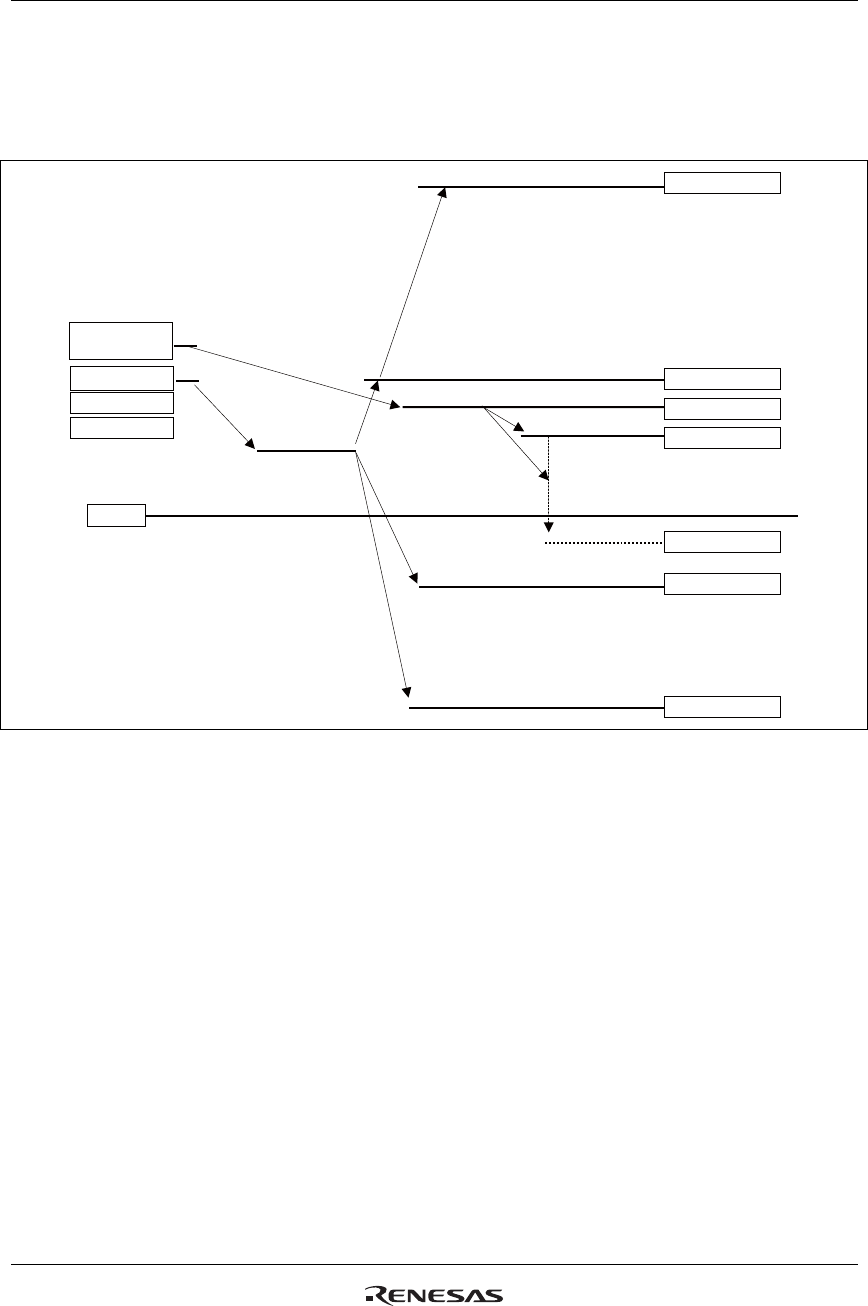
R61509V Target Spec
Rev. 0.11 April 25, 2008, page 152 of 181
Voltage Setting Pattern Diagram
The following are the diagrams of voltage generation in the R61509V and the TFT display application
voltage waveforms and electrical potential relationship.
VGH
BT
VC
VCI1
VREG1OUT
VCM/VCOMR
VRH
VREG1OUT
DDVDH
BT
VCOML
VDV
VGL
BT
VCL
㩷
VCOMH
IOVCC(1.65~3.3V)
GND(0V)
Internal reference
voltage (VCIR)
VCC(2.5~3.3V)
VCILVL(2.5~3.3V)
Figure 63
Notes: 1. The DDVDH, VGH, VGL, and VCL output voltages will become lower than their theoretical levels
(ideal voltages) due to current consumption at each output level. Make sure that output voltage
level in operation maintains the following relationships: (DDVDH – VREG1OUT) > 0.5V, (VCOML
– VCL) > 0.5V. Also make sure VGH-VGL ≤ 28V, VCI-VCL ≤ 6V. When the alternating cycle of
VCOM is high (e.g. polarity inverts every line cycle), current consumption will increase. In this
case, check the voltage before use.
2. In operation, setting voltages within the respective voltage ranges is recommended.
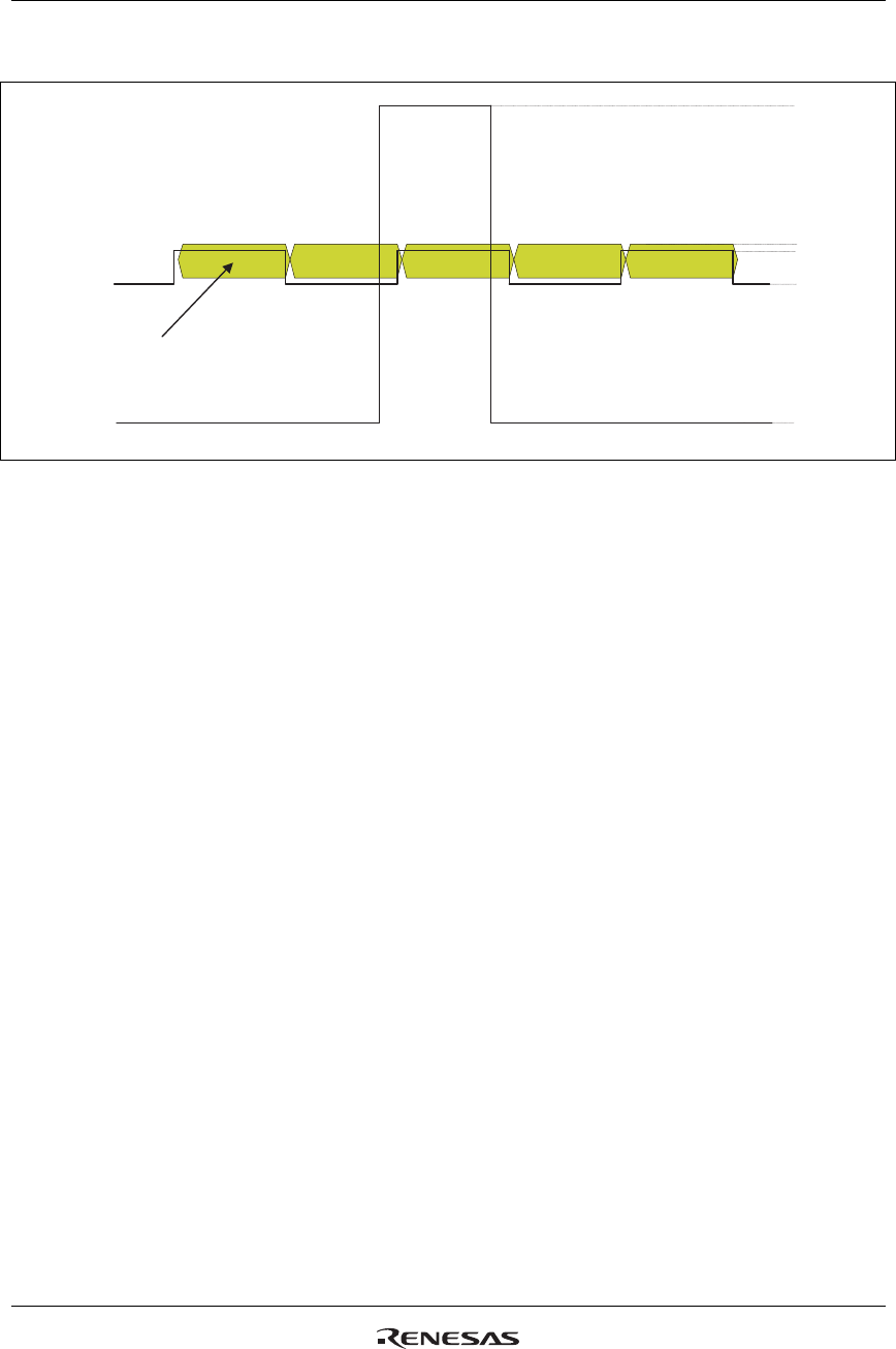
R61509V Target Spec
Rev. 0.11 April 25, 2008, page 153 of 181
Liquid Crystal Application Voltage Waveform and Electrical Potential
VCOM
Gn (panel interface output)
Sn (source driver output)
VGH
VREG1OUT
VCOMH
VCOML
Figure 64
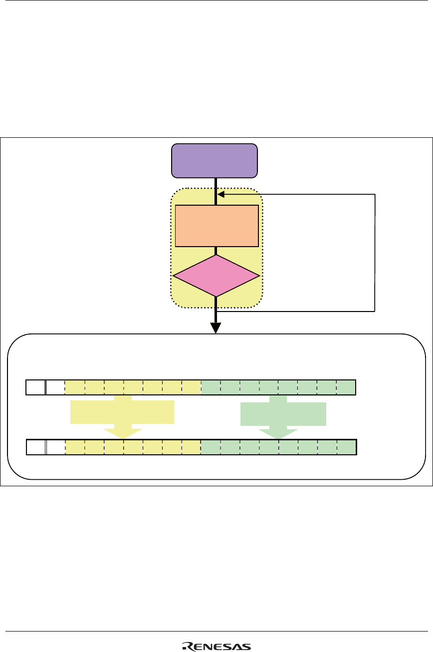
R61509V Target Spec
Rev. 0.11 April 25, 2008, page 154 of 181
VCOMH and VREG1OUT Voltage Adjustment Sequence
When adjusting the VCOMH voltage by setting VCM[6:0] (R280h, internal VCOMH level adjustment
circuit), follow the sequence below.
The R61509V can retain permanently the VREG1OUT and VCOMH level adjustment setting values in
NVM.
To write data to NVM, see “NVM Control” and NVM Write Sequence”.
㪠㫅㪻㪼㫏 㪈㪌 㪈㪋 㪈㪊 㪈㪉 㪈㪈 㪈㪇 㪐 㪏 㪎 㪍 㪌 㪋 㪊 㪉 㪈 㪇
㪍㪝㪈㪿
㩷
㩷
㩷
㪠㫅㪻㪼㫏 㪈㪌 㪈㪋 㪈㪊 㪈㪉 㪈㪈 㪈㪇 㪐 㪏 㪎 㪍 㪌 㪋 㪊 㪉 㪈 㪇
㪉㪏㪇㪿 㪭㪚㪤㩷
㪲㪍㪴 㩷
㪭㪚㪤㩷
㪲㪌㪴
㪭㪚㪤
㪲㪋㪴
㪭㪚㪤㩷
㪲㪊㪴
㪭㪚㪤㩷
㪲㪉㪴
㪭㪚㪤
㪲
㪈
㪴
㪭㪚㪤
㪲㪇㪴
㪬㪠㪛
㪲㪊㪴
㪬㪠㪛
㪲㪉㪴
㪬㪠㪛㩷
㪲㪇㪴
㪥㪭㪛㪘㪫㩷
㪲
㪈㪌
㪴
㪥㪭㪛㪘㪫㩷
㪲
㪈㪋
㪴
㪥㪭㪛㪘㪫㩷
㪲
㪈㪊
㪴
㪥㪭㪛㪘㪫
㪲
㪈㪉
㪴
㪥㪭㪛㪘㪫㩷
㪲
㪈㪈
㪴
㪥㪭㪛㪘㪫㩷
㪲
㪈㪇
㪴
㪥㪭㪛㪘㪫
㪲
㪐
㪴
㪥㪭㪛㪘㪫
㪲
㪏
㪴
㪥㪭㪛㪘㪫
㪲
㪎
㪴
㪥㪭㪛㪘㪫
㪲
㪍
㪴
㪥㪭㪛㪘㪫
㪲
㪌
㪴
㪥㪭㪛㪘㪫
㪲
㪋
㪴
㪥㪭㪛㪘㪫
㪲
㪊
㪴
㪥㪭㪛㪘㪫
㪲
㪉
㪴
㪥㪭㪛㪘㪫㩷
㪲
㪈
㪴
㪥㪭㪛㪘㪫㩷
㪲
㪇
㪴
㩷
㩷
㩷
㩷
㪬㪠㪛㩷
㪲㪈㪴
㩷
㩷
㪬㪠㪛
㪲㪎㪴
㪬㪠㪛
㪲㪍㪴
㪬㪠㪛
㪲㪋㪴
㪬㪠㪛
㪲㪌㪴
Display ON Sequence
Complete the VCOMH level adjustment.
The display on the panel will
flicker when the VCOMH
level is adjusted internally.
Set NVDAT[15] to 1.
NVM (1)
NVM Data Write Register
Set write data.
Adjust VCOMH
level
Set NVDAT[3:0] to the value set in
UID[7:0]. Then, write data to NVM.
Check the display
quality.
Set NVDAT[10:4] to the value set in the
VCM[6:0] after VCOMH level
adjustment. Then, write data to NVM.
VCOM level adjustment
R280h: VCM[6:0]
Set VCM[6:0] adjustment
value.
Figure 65
R61509V Target Spec
Rev. 0.11 April 25, 2008, page 155 of 181
NVM Control
The R61509V incorporates 16-bit NVM for user’s use.
• 7 bits are for VCOM adjustment (VCM register value is stored).
• 8 bits are for UID.
• 1 bit is for a dummy bit.
To write, read and erase data from/to the NVM, follow the sequences below. Data on the NVM is loaded to
internal registers automatically when the sequences are performed.
• Power On reset
• Exit shutdown mode
Data stored in the NVM is retained permanently even if power supply is turned off.
Table 81
Operation mode Power supply voltage (TBD) Time (TBD) Remarks Temperature
(TBD)
VPP1 9.2V±0.3V
Write
VPP3A Open or AGND
Write period:
150ms±50ms
- +20°C~+30C°
VPP1 9.2V±0.3V
Erase
VPP3A -9.2V±0.3V
Erase period:
10ms±1ms x n
time(s) (N ≤ 30, total
≤ 300ms)
Verify erase operation
at intervals of
10ms±1ms.
+20°C~+30C°
VPP1 Open or AGND Except
Write/Erase VPP3A Open or AGND
- - −40°C~+85C°
Note: NVM data rewrite (erase-write) operation should be performed up to 5 times per address.
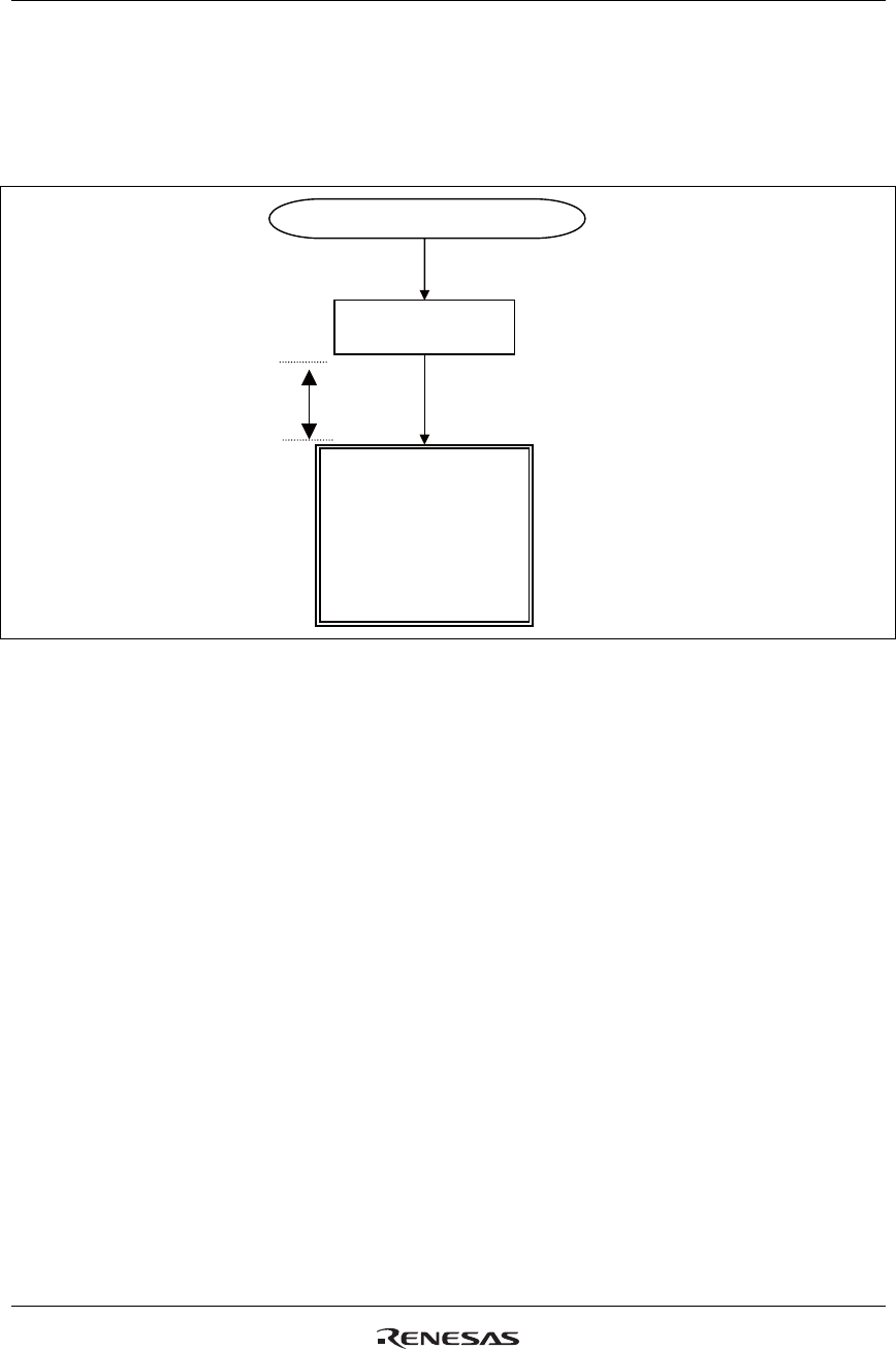
R61509V Target Spec
Rev. 0.11 April 25, 2008, page 156 of 181
NVM Load (Register Resetting) Sequence
Data on the NVM is loaded either automatically or by setting a command.
During the following sequence, the data written to the NVM is automatically loaded to the internal register.
NVM data read
Wait
1ms
or more
Except for the shutdown mode
Index: 6F0h
Command: 16’h0040
TE = 1’b0
CALB = 1’b1
EOP[1:0] = 2’b00
Index: 280h
VCM[6:0], UID[7:0]
Figure 66 NVM Load (Register Resetting) Sequence
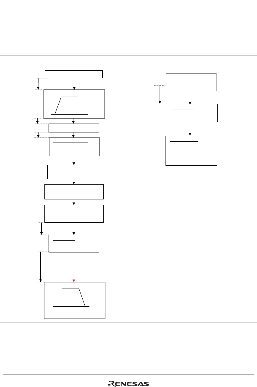
R61509V Target Spec
Rev. 0.11 April 25, 2008, page 157 of 181
NVM Write Sequence
Defined 16 bit data is written to the selected address. When “0” is written to these bits, the bits are set to
“0”. If the data is erased from the bit, the bit is returned to ”1”. The bit to which data is not written should
be set to “1”.
RS=0, DB=16’h0000
RS=0, DB=16’h0000
RS=0, DB=16’h0000
R
S
=
0,
DB=1
6
’h
0000
R6F1:16’h****
R6F0:16’h0010
(TE=0,CALB=0,EOP=2’h1)
R6F0:16’h0090
(TE=1,CALB=0,EOP=2’h1)
150msr50ms(TBD)
GND
VPP1=
9
.2r
0
.
3
V
VPP3A/VPP3B=GND
GND
VPP1
=
9.2
r
0.3
V
VPP3A =GND
6F0h:16’h0040
(CALB=1)
NVM Write Sequence NVM Load (Register Resetting) Sequence
1ms
or more
Power ON reset
Transfer synchronization
2msec
or more
1msec
or more
1msec
or more
NVM write setting
NVM write start
NVM write end
Power supply (VCC, VCI, IOVCC) ON
NVM write data set
1us
or more
(NVDAT=16’hXX (arbitrary data))
RA0: 16’h0000
(TE=0, EOP=2’h0,
NVAD=2’h0)
NVM load end
NVM load
(Automatically CALB = 0)
NVM data read
R280h: VCM[6:0], UID[7:0]
Instruction read
Figure 67 NVM Write Sequence
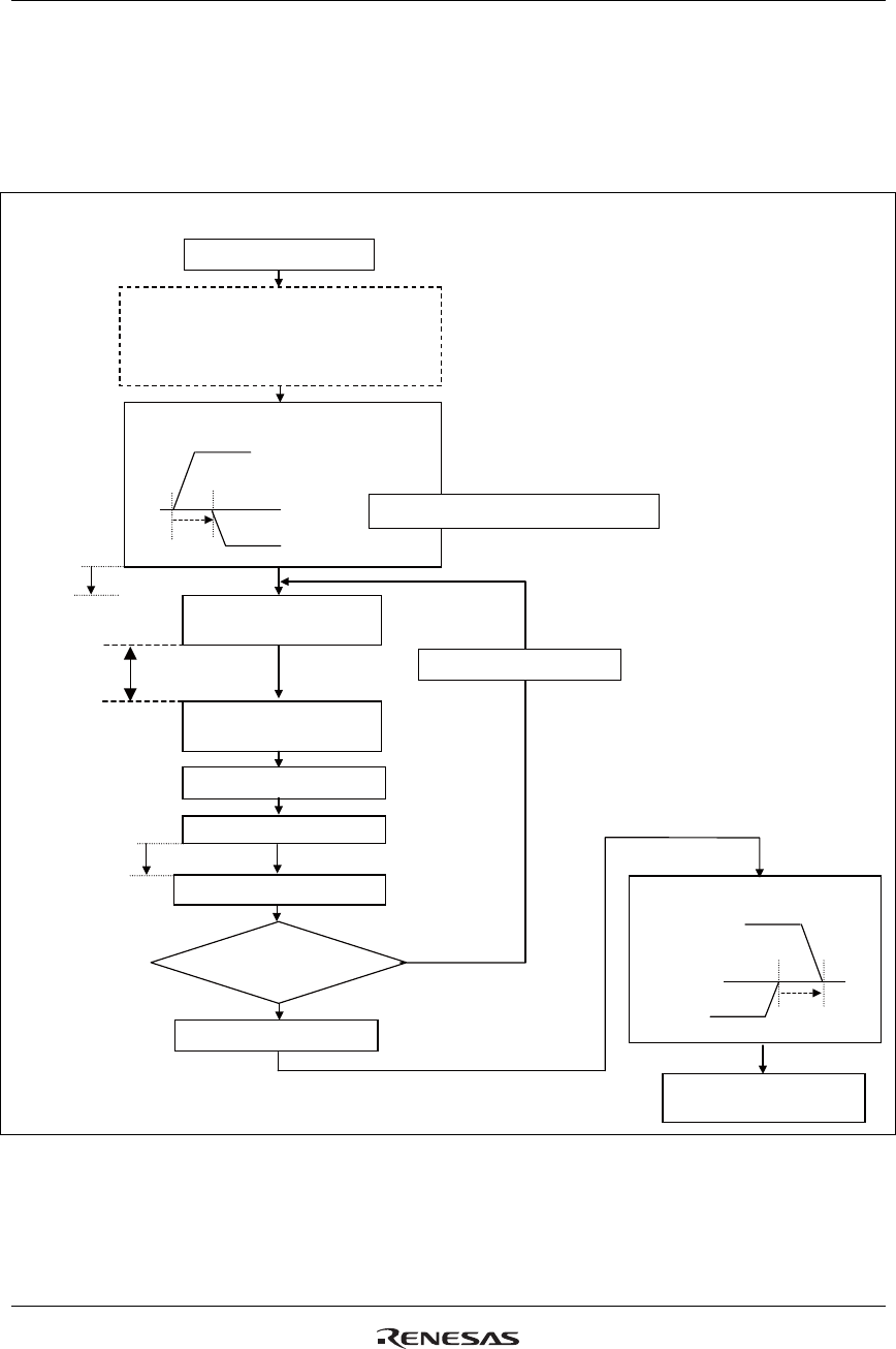
R61509V Target Spec
Rev. 0.11 April 25, 2008, page 158 of 181
NVM Erase Sequence
The data written to the selected 16 bits is erased all together. The bits from which data is erased are set to
“1”. To erase data from NVM, make sure VGL < VPP3A, and follow the sequence below after power
supply ON sequence.
㩷
㩷
㩷
㩷
㩷
㩷㩷
㪩㪍㪝㪇㪿
㪚㪘㪣㪙
㪔
㪈
㩷
㩷
NVM Erase Sequence
Power supply OFF
sequence
1ms or more
NVM erase power supply setting
To erase data from NVM, set the VC and BT bits
as follows to make sure VGL < VPP3A < -9.5V.
(R100h): BT[2:0] = 3’h6 (VGL = -10.8V)
(R101h): VC[2:0] = 3’h7 (VCI = 2.7V)
Power supply ON sequence
Fix VPP3B to GND.
Erase period
10ms±1ms
NVM power supply ON
NVM power supply OFF
1ms
or more
1ms
or more
1ms or more
VPP1 = 9.2±0.3V
VPP3A = -9.2±0.3V
GND
GND
R6F0h:
TE=1, EOP[1:0]=2’h03
R6F0h:
TE=0, EOP[1:0]=2’h00
R6F2h: NVVRF=1
R280h: NVM data read
R6F2h: NVVRF=0
VPP1 = 9.2±0.3V
VPP3 = -9.2±0.3V
NVM data read result:
15’h7FFF
NO
YES
Verify OFF
Verify ON
Start of rasing
End of erasing
R6F2h: NVVRF=0
Figure 68 NVM Erase Sequence
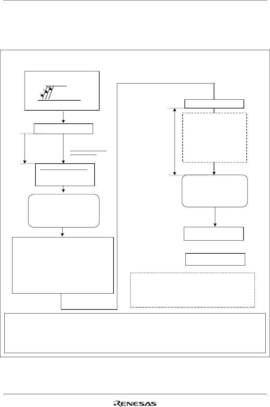
R61509V Target Spec
Rev. 0.11 April 25, 2008, page 159 of 181
Power Supply Setting Sequence
The following are the sequences for setting power supply ON/OFF instructions. Set power supply ON/OFF
instructions according to the following sequences in Display ON/OFF, Sleep set/exit sequences.
㪭㪚㪚
㪠
㪦㪭㪚㪚
㪭㪚
㪠
㪞
㪥㪛
㩷
㩷
㩷
㩷
Power Supply ON Sequence
Notes: 1. Set VCMR to 1 when using internal electric volume.
2. When NVM is in the status that the R61509V is shipped out, set the instruction register (R280h: VCM[6:0], and
UID[7:0]). If writing values to VCM[6:0] and UID[7:0] has been completed, setting this instruction register is
unnecessary.
(A) Liquid crystal
power supply OFF
(DCDC OFF) state
Display OFF state
(B) Liquid crystal
power supply ON
(DCDC ON) state
Display OFF state
OR
R102h: PSON=1, PON=1
Power ON reset
Transfer synchronization
1ms
or more
Power supply (VCC, VCI, IOVCC) ON
VCC → IOVCC → VCI
or VCC, IOVCC, VCI simultaneously
Display ON sequence
NVM erase sequence
Instruction user setting
R400h: NL[5:0]
R008h: BP[7:0], FP[7:0]
R300h~R309h: γ control
R010h: RTNI[4:0], DIVI[1:0]
R100h: BT[2:0], AP[1:0]
R101h: VC[2:0], DC0[2:0], DC1[2:0]
Other user settings: see notes 1 and 2.
RS=0, DB=16’h0000
RS=0, DB=16’h0000
RS=0, DB=16’h0000
RS=0, DB=16’h0000
Power supply startup time
(6 frames x 1/osc)
(1) Other mode setting instruction
(2) RAM write instruction,
etc.
Automatic NVM data load
Access is prohibited
1ms after reset.
(1) To turn the display on, follow “Display ON Sequence”
in “Instruction Setting Sequence and Refresh Sequence”.
(2) To erase data from NVM, follow “NVM Erase Sequence”.
Erase data from NVM according to “NVM Control”.
Figure 69
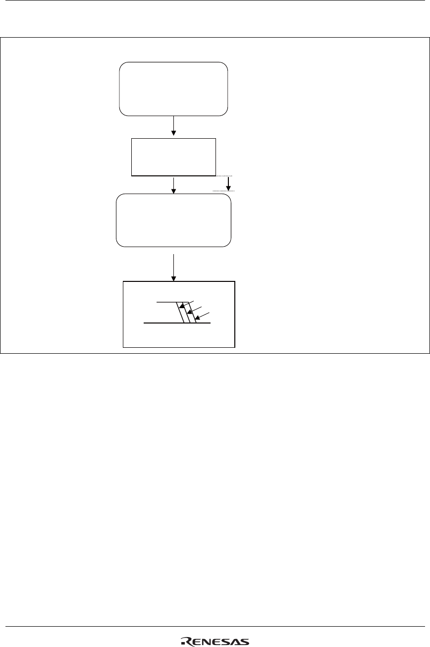
R61509V Target Spec
Rev. 0.11 April 25, 2008, page 160 of 181
ޣᶧ᥏㔚Ḯ
ࠝࡈࡈࡠ
ޤ
R102h: PON=0PSON=0
㪞
㪥㪛
Power Supply OFF Sequence
5 frames or more
(A) Liquid crystal
power supply OFF
(DCDC OFF)
Display OFF state
(B) Liquid crystal
power supply ON
(DCDC ON) state
Display OFF state
VCI → IOVCC → VCC
or VCC, IOVCC, VCI simultaneously
Power supply (VCC, VCI, IOVCC) OFF
IOVCC
VCC
VCI
Figure 70

R61509V Target Spec
Rev. 0.11 April 25, 2008, page 161 of 181
Notes to Power Supply ON Sequence
When voltages do not rise in the order of VCC, IOVCC and then VCI and have to change the order, please
follow the following note.
Note
Internal operation of the R61509V is unstable until VCC rises. If IOVCC rose before VCC rises, the
R61509V may be in “output” status. In this case, do not send or receive any data before power supply is
completed.
Changing order of voltage input will not cause troubles such as latchup or destruction of the LSI.
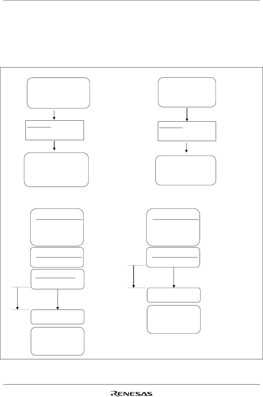
R61509V Target Spec
Rev. 0.11 April 25, 2008, page 162 of 181
Instruction Setting Sequence and Refresh Sequence
Display ON/OFF Sequences and Refresh Sequence
In setting instruction in the R61509V, follow the sequences below. To reduce malfunction caused by noise,
execute refresh sequence 1 regularly. To exit shutdown mode, execute refresh sequence 2.
㩷
㩷
㩷
㩷
㩷
㩷
㩷
㩷
㩷
㩷
Note: For power supply setting, see “Power Supply Setting Sequence”.
Display ON sequence Display OFF sequence
Refresh Sequence 1 Refresh Sequence 2
0.1ms
or more
0.3ms
or more
(B) Liquid crystal
power supply ON
(DCDC ON) state
Display OFF state
(C) Liquid crystal
power supply ON
(DCD ON) state
Display ON state
(B) Liquid crystal
power supply ON
(DCDC ON) state
Display OFF state
(C) Liquid crystal
power supply ON
(DCD ON) state
Display ON state
Display ON Display OFF
R007h: BASEE=1 R007h: BASEE=0
Transfer synchronization Transfer synchronization
RS=0, DB=16’h0000
RS=0, DB=16’h0000
RS=0, DB=16’h0000
RS=0, DB=16’h0000
RS=0, DB=16’h0000
RS=0, DB=16’h0000
RS=0, DB=16’h0000
RS=0, DB=16’h0000
Except the following instructions:
R600h: TRSR
R6F0h: CALB
R6F1h: NVDAT[15:0]
Except the following instructions:
R600h: TRSR
R6F0h: CALB
R6F1h: NVDAT[15:0]
NVM data load
All instruction initial setting
and user setting
Test register initialization Test register initialization
R600h: TRSR=1 R600h: TRSR=1
R6F0h: CALB=1
R600h: TRSR=0
R600h: TRSR=0
All instruction initial setting
and user setting
Figure 71
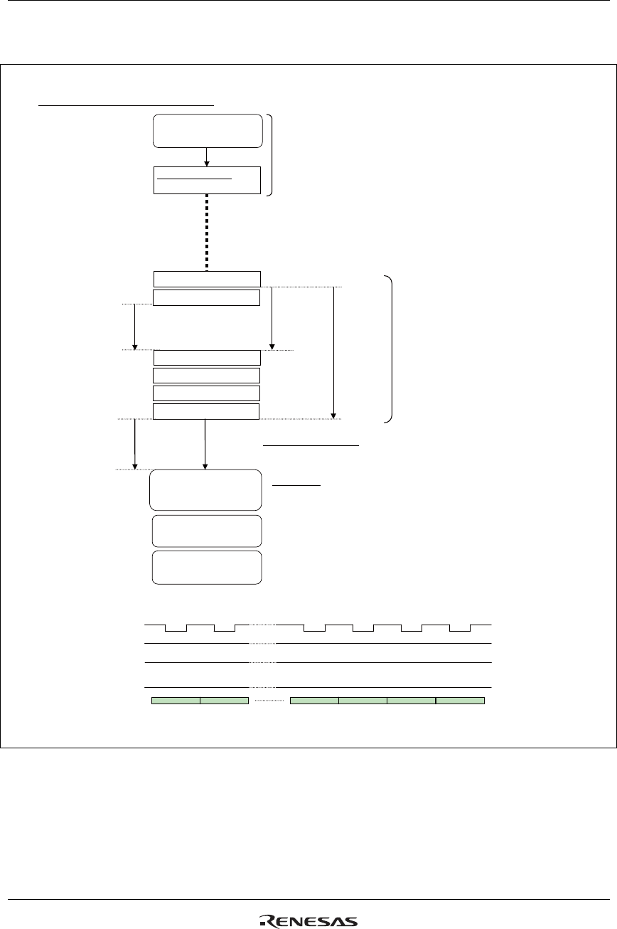
R61509V Target Spec
Rev. 0.11 April 25, 2008, page 163 of 181
Shutdown Mode Sequences
CSX=”Low”
(
1
)
CSX=”Low”
(
2
)
CSX=”Low”
(
3
)
CSX=”Low”
(
4
)
CSX=”Low”
(
5
)
CSX=”Low”
(
6
)
㩷
㩷
㩷
㩷
Waveforms in Exiting Shutdown Mode (Input CSX="Low")
Notes: 1. See AC characteristics in Electrical Characteristics for details on low width (PWLW), high width (PWHW), and cycle (tCYCW) periods.
2. Leave at least 1 ms between the 2nd and 3rd inputs of CSX = Low in exiting shutdown mode.
Shutdown Sequence (Exit shutdown mode by inputting CSX = “Low”)
18-/16-/9-/8-bit interface operation
VDD startup,
Oscillation startup period
Exit shutdown mode
Input CSX = “Low” 6 times.
Initialize the
R61509V.
Automatic NVM data load
1ms
or more
0.3ms
or more
Display OFF sequence
Display ON sequence
RAM data setting
Data and RS = Don’t care
Refresh sequence 2
“High”
“High”
“Low” or “High”
Don’t care Don’t care Don’t care Don’t care Don’t care Don’t care
Set shutdown mode
R100h: DSTB=1
Set shutdown mode
CSX
RDX
RS
Data
User setting
NL, BP, FP, γ control,
RTNI, DIVI, and others
Executing refresh sequence
regularly is recommended.
123456
Wait
1ms.
WRX
Figure 72
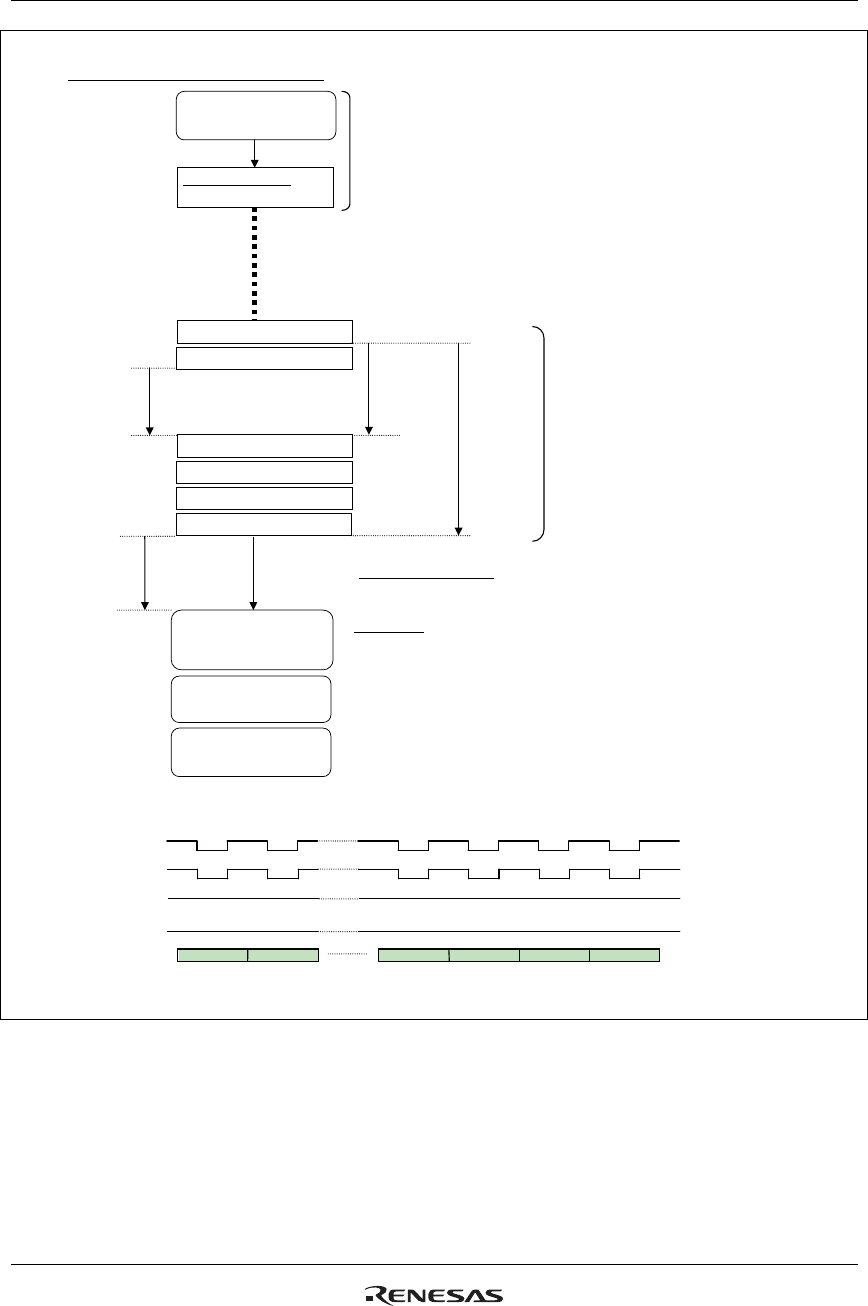
R61509V Target Spec
Rev. 0.11 April 25, 2008, page 164 of 181
Index Write
(
Data=16’h0000
)
Index Write
(
Data=16’h0000
)
Index Write
(
Data=16’h0000
)
Index Write
(
Data=16’h0000
)
Index Write
(
Data=16’h0000
)
Index Write
(
Data=16’h0000
)
㩷
Automatic NVM data load
Set shutdown mode
Notes: 1. See AC characteristics in Electrical Characteristics for details on low width (PWLW), high width (PWHW), and cycle (tCYCW) periods.
2. Leave 1 ms or more between the 2nd and 3rd inputs of Index Write.
“High”
“Low”
16’h0000 16’h0000 16’h0000 16’h0000 16’h0000 16’h0000
CSX
WRX
RDX
RS
Data
1ms
or more
0.3ms
or more
RAM data setting
Display ON sequence
Display OFF sequence
VDD startup,
Oscillation startup period
Initialize the
R61509V.
Refresh sequence 2
Set shutdown mode
R100h: DSTB=1
Exit shutdown mode
123456
Wait
1ms.
User setting
NL, BP, FP, γ control,
RTNI, DIVI, and others
Executing refresh sequence
regularly is recommended.
Shutdown Sequence (Exit shutdown mode by inputting CSX = “Low” and WRX = “Low” (Index Write))
(1) 18-/16-bit interface operation
Waveforms in Exiting Shutdown Mode (Input RS = “Low”and Index Write)
Figure 73
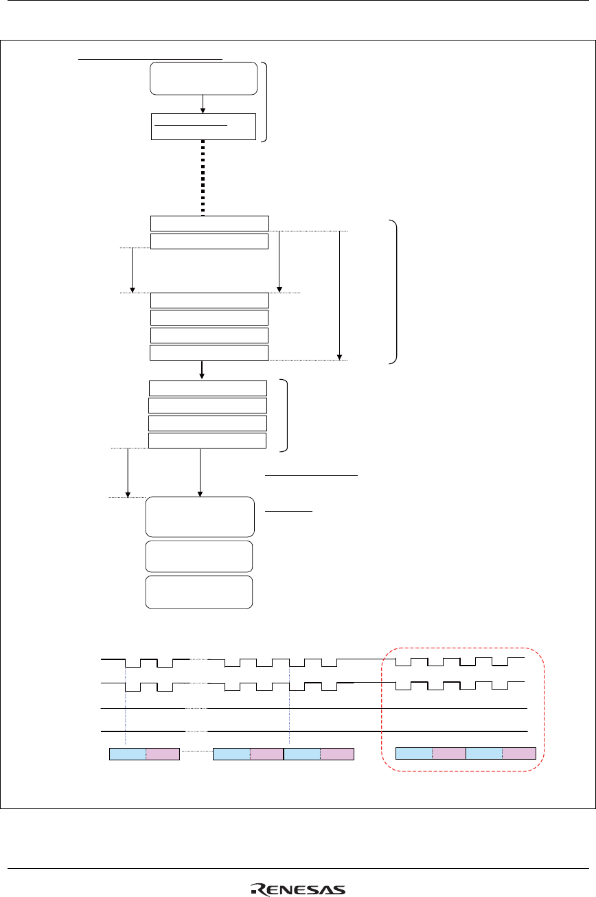
R61509V Target Spec
Rev. 0.11 April 25, 2008, page 165 of 181
Index Write
(
Data=8’h00
)
Index Write
(
Data=8’h00
)
Index Write
(
Data=8’h00
)
Index Write
(
Data=8’h00
)
Index Write
(
Data=8’h00
)
Index Write
(
Data=8’hFF
)
Index Write
(
Data=8’h00
)
Index Write
(
Data=8’h00
)
Index Write
(
Data=8’h00
)
Index Write
(
Data=8’h00
)
㩷
㩷
㩷 㩷
㩷
㩷
㩷
㩷
㩷
Notes: 1. See AC characteristics in Electrical Characteristics for details on low width (PWLW), high width (PWHW), and cycle (tCYCW) periods.
2. Leave at least 1 ms between the 2nd and 3rd Index write.
3. Set transfer synchronous command data 8'h00 when using 8 bit interface and 9'h000 when using 9-bit interface.
RAM data setting
Display ON sequence
Refresh sequence 2
VDD startup,
Oscillation startup period
Initialize the
R61509V.
Set shutdown mode
Display OFF sequence
Exit shutdown mode
(2) 9-/8-bit interface operation
0.3ms
or more
1ms
or more
Automatic NVM data load
RS
Data
“High”
“Low”
00h 00h 00h
00h
00h FFh 00h 00h 00h 00h
Upper IW Lower IW Upper IW Upper IW Upper IW Upper IW
Lower IW Lower IW Lower IW Lower IW
Set shutdown mode
R100h: DSTB=1
Transfer synchronization command (see note 3)
User setting
NL, BP, FP, γ control,
RTNI, DIVI, and others
Executing refresh sequence
regularly is recommended.
Transfer synchronization
1234561234
Waveforms in Exiting Shutdown Mode (Input RS = “Low”and Index Write)
Wait
1ms.
Execute transfer synchronization command by inputting RS = “Low” and Index Write after exiting shutdown mode.
CSX
WRX
RDX
Figure 74
R61509V Target Spec
Rev. 0.11 April 25, 2008, page 166 of 181
8-Color Mode Setting
R00Bh: COL=1
262,144-color mode
display
8-color mode display
8 color to 262,144 color mode
R00Bh: COL=0
262,144-color mode
display
8-color mode display
262,144 color to 8 color mode
Figure 75
Partial Display Setting
Partial Display Setting Sequence
Partial display setting
R500h: PTDP[8:0]
R501h: PTSA[8:0]
R502h: PTEA[8:0]
Partial display
Full-screen display
Set as required
Full-screen display
8-color display, low power
consumption settings
R007h: COL=1,
R009h: PTS
Base image display ON
Partial display OFF
R007h: BASEE=1, PTDE=0
Base image display OFF
Partial display ON
R007h: BASEE=0, PTDE=1
Figure 76
R61509V Target Spec
Rev. 0.11 April 25, 2008, page 167 of 181
Absolute Maximum Ratings
Table 82
Notes: 1. If used beyond the absolute maximum ratings, the LSI may be permanently damaged. It is
strongly recommended to use the LSI under the condition within the electrical characteristics in
normal operation. If exposed to the condition not within the electrical characteristics, it may affect
the reliability of the device.
2. Make sure VCC≥GND, and IOVCC≥GND.
3. Make sure VCI≥AGND.
4. Make sure DDVDH ≥ AGND.
5. Make sure DDVDH≥VCL.
6. Make sure AGND≥VGL.
7. Make sure VCI≥VGL.
8. The DC/AC characteristics of the die and wafer products are guaranteed at 85℃.
Items Symbol Unit Value Note
Power supply voltage 1 VCC, IOVCC V -0.3 ~ +4.6 1, 2
Power supply voltage 2 VCI – AGND V -0.3 ~ +4.6 1, 3
Power supply voltage 3 DDVDH – AGND V -0.3 ~ +6.5 1, 4
Power supply voltage 4 AGND – VCL V -0.3 ~ +4.6 1
Power supply voltage 5 DDVDH – VCL V -0.3 ~ +9.0 1, 5
Power supply voltage 7 AGND– VGL V -0.3 ~ +13.0 1, 6
Power supply voltage 8 VGH – VGL V -0.3 ~ +30.0 1
Power supply voltage 9 VCI – VGL V -0.3 ~ +6.5 1, 7
Power supply voltage 10 VPP1 V -0.3 ~ +10.0 1
Power supply voltage 11 VPP3A V -0.3 ~ +0.3 1
Input voltage Vt V -0.3 ~ IOVCC + 0.3 1
Operation temperature Topr ℃ -40 ~ +85 1, 8
Storage temperature Tstg ℃ -55 ~ +110 1
R61509V Target Spec
Rev. 0.11 April 25, 2008, page 168 of 181
Electrical Characteristics
DC Characteristics
(VCC= 2.50V~3.30V, VCI=2.50V~3.30V, IOVCC=1.65V~3.30V, Ta= -40°C~+85°C *See note 1)
Table 83
Items Symbol Unit Test condition Min. Typ. Max. Notes
Input high-level voltage VIH V
IOVCC=1.65V~3.30V 0.80×
IOVCC - IOVCC 2, 3
Input low-level voltage VIL V
IOVCC=1.65V~3.30V -0.3 - 0.20×
IOVCC 2, 3
Output high voltage 1
(DB0-17,FMARK) VOH1 V IOVCC=1.65V~3.30V,
IOH=-0.1mA
0.8×
IOVCC - - 2
Output low voltage 1
(DB0-17,FMARK) VOL1 V IOVCC=1.65V~3.30V,
IOL=0.1mA - - 0.20×
IOVCC 2
I/O leakage current ILI1 µA
Vin=0~IOVCC -1 - 1 4
Current consumption
((IOVCC-IOGND)+
(VCC-GND))
Normal operation mode (262,144 color
display)
IOP1 µA
fosc=678kHz (432-line drive), I80-IF,
IOVCC=VCC=3.00V, fFLM=60Hz,
Ta=25℃, RAM data: 18’h000000, See
other as well.
- 600 TBD 5, 6
Current consumption
((IOVCC-IOGND)+
(VCC-GND))
8-color, 64-line partial display on sub
display
Iop2 µA
fosc=678kHz (64-line partial display),
IOVCC=VCC=3.00V, fFLM=40Hz,
Ta=25℃, RAM data: 18h’000000, see
other as well.
- 300 - 5, 6
Current consumption
((IOVCC-IOGND)+
(VCC-GND))
Shutdown mode
Ishut1 µA
IOVCC=VCC=3.00V, I80-IF, Ta=25℃ - 0.1 1.0 5, 6
Current consumption
((IOVCC-IOGND)+
(VCC-GND))
RAM access mode 1
IRAM1 mA
IOVCC=2.40V, VCC=3.00V,
tCYCW=110ns, Ta=25℃, I80-8bit-I/F,
TRIREG=1’h1, Consecutive RAM access
during display operation, BC0=0, FP=5,
BP=8, γ register; 0(default), COL=0
- 3.0 - 5
LCD power supply current (VCI-GND)
262,144-color display Ici1 mA
IOVCC=1.8V, VCC=VCI=2.8V,
432-line drive, fFLM=60Hz, Ta=25℃,
Frame memory data: 18’h00000, REV=0,
BC0=0, FP[7:0]=8’h8, BP[7:0]=8’h8,
VC[2:0]=3’h1, BT[2:0]=3’h2,
VRH[4:0]=5’h18, VCM[6:0]=7’h7F,
VDV[4:0]=5’h11, AP[1:0]=2’h3,
DC0[2:0]=3’h3, DC1[2:0]=3’h4,
PR*P00=PR*N00=5’h00,
PR*P01=PR*N01=5’h02,
PR*P02=PR*N02=5’h04,
PR*P03=PR*N03=4’h8,
PR*P04=PR*N04=4’hF,
PR*P05=PR*N05=4’h8,
PR*P06=PR*N06=5’h04,
PR*P07=PR*N07=5’h02,
PR*P08=PR*N08=5’h04,
PIR*P0= PIR*P1= PIR*P2= PIR*P3=2'h0
PIR*N0= PIR*N1= PIR*N2= PIR*N3=2'h0
(*: 0, 1, 2)
No load on the panel.
- 3.5 TBD 6

R61509V Target Spec
Rev. 0.11 April 25, 2008, page 169 of 181
LCD power supply current (VCI-GND)
8-color, 64-line partial display
Ici2 mA
IOVCC=1.8V, VCC=VCI=2.8V,
64-line partial, fFLM=40Hz, Ta=25℃,
Frame memory data: 18’h00000, REV=0,
BC0=0, FP[7:0]=8’h8, BP[7:0]=8’h8,
VC[2:0]=3’h1, BT[2:0]=3’h2,
VRH[4:0]=5’h18, VCM[6:0]=7’h7F,
VDV[4:0]=5’h11, AP[1:0]=2’h3,
DC0[2:0]=3’h3, DC1[2:0]=3’h4,
PR*P00=PR*N00=5’h00,
PR*P01=PR*N01=5’h02,
PR*P02=PR*N02=5’h04,
PR*P03=PR*N03=4’h8,
PR*P04=PR*N04=4’hF,
PR*P05=PR*N05=4’h8,
PR*P06=PR*N06=5’h04,
PR*P07=PR*N07=5’h02,
PR*P08=PR*N08=5’h04,
PIR*P0= PIR*P1= PIR*P2= PIR*P3=2'h0
PIR*N0= PIR*N1= PIR*N2= PIR*N3=2'h0
(*: 0, 1, 2)
No load on the panel.
- 0.8 TBD 5, 6
VPP1-
AGND IVPP1W mA - - 30.0 6
NVM current
consumption Write VPP3A-
AGND IVPP3AW mA
VPP1=9.2V
VPP3A=GND
(Write period) - - 1.0 6
VPP1-
AGND IVPP1E mA - - 1.0 6
NVM current
consumption Erase VPP3A-
AGND IVPP3AE mA
VPP1=9.2V
VPP3A=-9.2V
(Erase period) - - 1.0 6
Output voltage dispersion ΔVO mV - - 5 - 7
Average output variance ΔVΔ mV - -35 - 35 8

R61509V Target Spec
Rev. 0.11 April 25, 2008, page 170 of 181
Step-up Circuit Characteristics
Table 84
Item Unit Test condition Min. Typ. Max. Note
DDVDH V
IOVCC=VCC=VCI=2.80[V], fosc=678[kHz], Ta=25℃,
VC=3’h1, AP=3’h3, BT=3’h2, DC0=3’h4 (div. 1/8),
DC1=3’h2 (div. 1/4), COL=0, D=2’h0,
C11=C12=C13=C21=C22=1[uF]/B characteristics,
DDVDH=VGH=VGL=VCL=1[uF]/B characteristics,
Iload1=-3 [mA], No load on the panel.
4.8 5.1 - -
VGH V
IOVCC=VCC=VCI=2.80[V], fosc=678[kHz], Ta=25℃,
VC=3’h1, AP=3’h3, BT=3’h2, DC0=3’h4 (div. 1/8),
DC1=3’h2 (div. 1/4), COL=0, D=2’h0,
C11=C12=C13=C21=C22=1[uF]/B characteristics,
DDVDH=VGH=VGL=VCL=1[uF]/B characteristics,
Iload2=-100[uA], No load on the panel.
14.4 15.1 - -
VGL V
IOVCC=VCC=VCI=2.80[V], fosc=678[kHz], Ta=25℃,
VC=3’h1, AP=3’h3, BT=3’h2, DC0=3’h4 (div. 1/8),
DC1=3’h2 (div. 1/4), COL=0, D=2’h0,
C11=C12=C13=C21=C22=1[uF]/B characteristics,
DDVDH=VGH=VGL=VCL=1[uF]/B characteristics,
Iload3=+100[uA], No load on the panel.
- -10.0 -9.6 -
Step-up
output
voltage
VCLV V
IOVCC=VCC=VCI=2.80[V], fosc=678[kHz], Ta=25℃,
VC=3’h1, AP=3’h3, BT=3’h2, DC0=3’h4 (div. 1/8),
DC1=3’h2 (div. 1/4), COL=0, D=2’h0,
C11=C12=C13=C21=C22=1[uF]/B characteristics,
DDVDH=VGH=VGL=VCL=1[uF]/B characteristics,
Iload4=+200[uA], No load on the panel.
- -2.55 -2.4 -
Internal Reference Voltage: Condition
(VCC= 2.50V~3.30V, Ta= -40°C~+85°C)
Table 85
Item Symbol
Unit Min. Typ. Max.
Note
Internal reference
voltage VCIR V - 2.50 - 12
R61509V Target Spec
Rev. 0.11 April 25, 2008, page 171 of 181
Power Supply Voltage Range
(Ta= -40°C~+85°C, GND=AGND=0V)
Table 86
Item Symbol
Unit Min. Typ. Max. Condition
Power Supply Voltage IOVCC V 1.65 1.80/2.80 3.30 -
Power Supply Voltage VCC V 2.50 2.80 3.30 -
Power Supply Voltage VCI V 2.50 2.80 3.30 -
V 8.9 9.2 9.5 Write
Power Supply Voltage VPP1 V 8.9 9.2 9.5 Erase
V -0.3 0.0 +0.3 Write
Power Supply Voltage VPP3A V -9.5 -9.2 -8.9 Erase
Output Voltage Range
(Ta= -40°C~+85°C, GND=AGND=0V)
Table 87
Item Symbol
Unit Min. Typ. Max. Condition
Grayscale, VCOM
reference
VREG1O
UT V - - DDVDH-0.5 -
Source driver V GND+0.2 - VREG1OUT -
VCOMH output VCOMH V - - VREG1OUT -
VCOML output VCOML V VCL+0.5 - - -
VCOM amplitude V - - 6.0 -
Step-up output DDVDH V 4.5 - 6.0 -
Step-up output VGH V 10.0 - 18.0 -
Step-up output VGL V -13.5 - -4.5 -
Step-up output VCL V -3.0 - -1.9 -
VCI-VCL V - - 6.0 -
VGH-VGL V - - 28.0 -
R61509V Target Spec
Rev. 0.11 April 25, 2008, page 172 of 181
AC Characteristics
(VCC= 2.50V~3.30V, IOVCC=1.65V~3.30V, Ta= -40°C~+85°C *See note 1)
Clock Characteristics
Table 88
Item Symbol Unit Test condition Min. Typ. Max. Note
Oscillation clock fosc kHz VCC=IOVCC=3.0V 631 678 725 9
80-system 18-/16-/9-/8-bit Bus interface Timing Characteristics
(1-/2-/3-transfer, IOVCC=1.65V~3.30V) TBD
Table 89
Items Symbol Unit
Test
condition Min. Typ. Max.
Write tCYCW ns Figure A 75
(TBD) - -
Bus cycle time
Read tCYCR ns Figure A 450 (TBD) - -
Write low- level pulse width PWLW ns Figure A 30
(TBD) - -
Read low-level pulse width PWLR ns Figure A 170 (TBD) - -
Write high-level pulse width PWHW ns Figure A 25 (TBD) - -
Read high-level pulse width PWHR ns Figure A 250 (TBD) - -
Write/ Read rise/fall time tWRr,
WRf ns Figure A - - 15
Write (RS to CSX,
WRX) ns Figure A 0 (TBD) - -
Setup time
Read (RS to CSX,
RDX)
tAS
ns Figure A 10 (TBD) - -
Address hold time tAH ns Figure A 2 (TBD) - -
Write data setup time tDSW ns Figure A 25
(TBD) - -
Write data hold time tH ns Figure A 10 (TBD) - -
Read data delay time tDDR ns Figure A - - 150
Read data hold time tDHR ns Figure A 5 (TBD) - -
R61509V Target Spec
Rev. 0.11 April 25, 2008, page 173 of 181
Clock Synchronous Serial Interface Timing Characteristics
(IOVCC=1.65V~3.30V) TBD
Table 90
Item Symbol Unit Test condition Min. Typ. Max.
Write (receive) tSCYC ns Figure B 100 (TBD) - 20,000
Serial clock cycle
time Read (transmit) tSCYC ns Figure B 350
(TBD) - 20,000
Write (receive) tSCH ns Figure B 40 (TBD) - -
Serial clock
high-level width Read (transmit) tSCH ns Figure B 150
(TBD) - -
Write (receive) tSCL ns Figure B 40 (TBD) - -
Serial clock
low-level width Read (transmit) tSCL ns Figure B 150
(TBD) - -
Serial clock rise/fall time tSCr,tSCf ns Figure B - - 15 (TBD)
Chip select setup time tCSU ns Figure B 20 (TBD) - -
Chip select hold time tCH ns Figure B 60 (TBD) - -
Serial input data setup time tSISU ns Figure B 30 (TBD) - -
Serial input data hold time tSIH ns Figure B 30 (TBD) - -
Serial output data delay time tSOD ns Figure B - - 130
(TBD)
Serial output data delay time tSOH ns Figure B 5 (TBD) - -
RGB Interface Timing Characteristics
(18-/16-bit RGB interface, IOVCC=1.65V~3.30V) TBD
Table 91
Item Symbol Unit Test condition Min. Typ. Max.
VSYNC/HSYNC setup time tSYNCS clock Figure D 0.5 (TBD) - 1.5
ENABLE setup time tENS ns Figure D 10 (TBD) - -
ENABLE hold time tENH ns Figure D 20 (TBD) - -
DOTCLK low-level pulse width PWDL ns Figure D 40 (TBD) - -
DOTCLK high-level pulse width PWDH ns Figure D 40 (TBD) - -
DOTCLK cycle time tCYCD ns Figure D 100 (TBD) - -
Data setup time tPDS ns Figure D 10 (TBD) - -
Data hold time tPDH ns Figure D 40 (TBD) - -
DOTCLK, VSYNCX and HSYNCX
rise/fall time
trgbr,
trgbf ns Figure D
- - 15

R61509V Target Spec
Rev. 0.11 April 25, 2008, page 174 of 181
LCD Driver Output Characteristics
Table 92
Item Symbol Unit Test condition Min. Typ. Max. Note
Source driver
output delay time tdds µs
VCC=IOVCC =2.80V, VC[2:0]=3’h7
VRH[4:0]=5’h1F,
fosc=678kHz (432-line drive), Ta=25°C,
PR*P00=PR*N00=5’h00,
PR*P01=PR*N01=5’h02,
PR*P02=PR*N02=5’h04,
PR*P03=PR*N03=4’h8,
PR*P04=PR*N04=4’hF,
PR*P05=PR*N05=4’h8,
PR*P06=PR*N06=5’h04,
PR*P07=PR*N07=5’h02,
PR*P08=PR*N08=5’h04,
PIR*P0= PIR*P1= PIR*P2= PIR*P3=2'h0
PIR*N0= PIR*N1= PIR*N2= PIR*N3=2'h0
Same change from the same grayscale at
all time-division source output pins.
Time to reach the target voltage ±35mV
from VCOM polarity inversion timing.
R=10kohm, C=30pF
- 25
(TBD) - 10
VCOM output
delay time tddv µs
VCC=IOVCC=2.80V, VC[2:0]=3’h7,
VRH[4:0] =5’h1F,
fosc=678kHz (432-line drive), Ta=25°C,
PR*P00=PR*N00=5’h00,
PR*P01=PR*N01=5’h02,
PR*P02=PR*N02=5’h04,
PR*P03=PR*N03=4’h8,
PR*P04=PR*N04=4’hF,
PR*P05=PR*N05=4’h8,
PR*P06=PR*N06=5’h04,
PR*P07=PR*N07=5’h02,
PR*P08=PR*N08=5’h04,
PIR*P0= PIR*P1= PIR*P2= PIR*P3=2'h0
PIR*N0= PIR*N1= PIR*N2= PIR*N3=2'h0
Time to reach ±35mV when shifting
between source V0⇔V63 in the worst
case of scenario.
R=100ohm, C=10nF
- 25 (TBD) - 11
Reset Timing Characteristics
Table 93(IOVCC=1.65V~3.30V)
Item Symbol Unit Test condition Min. Typ. Max.
Reset ”Low” level width tRES ms Figure C 1 - -
Reset rise time trRES µs Figure C - - 10
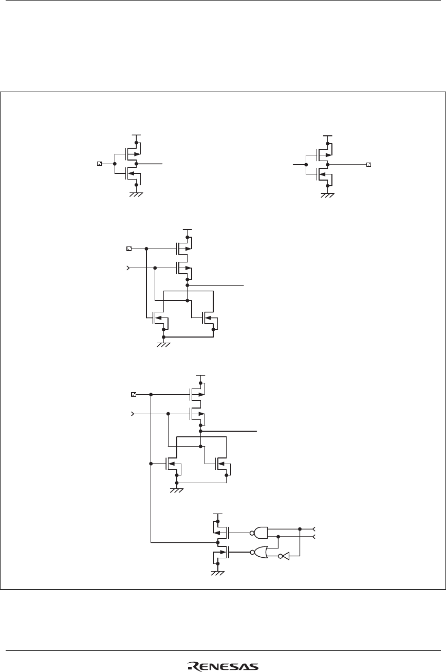
R61509V Target Spec
Rev. 0.11 April 25, 2008, page 175 of 181
Notes to Electrical Characteristics
Note 1. The DC/AC electrical characteristics of bare die and wafer products are guaranteed at 85℃.
Note 2. The following figures illustrate the configurations of input, I/O, and output pins.
GND
Output data
IOVCC
IOVCC IOVCC
IOVCC
IOVCC
GND GND
GND
GND
PMOS PMOS
PMOS
PMOS
PMOS
PMOS
PMOS
NMOS NMOS
NMOS
NMOS
NMOS
NMOS
NMOS
(Input circuit)
(Input circuit)
(Input circuit)
Pins: WR_SCL, RDX
Pins: DB17-DB0
Pins: FMARK, SDO
Pins: RESETX, IM2-1, IM0_ID
VSYNCX, HSYNCX, DOTCLK, ENABLE,
CSX, RDX, SDI
Input enable (CSX)
Input enable (CSX)
(Output circuit: three states)
Output enable
Output data
Figure 77
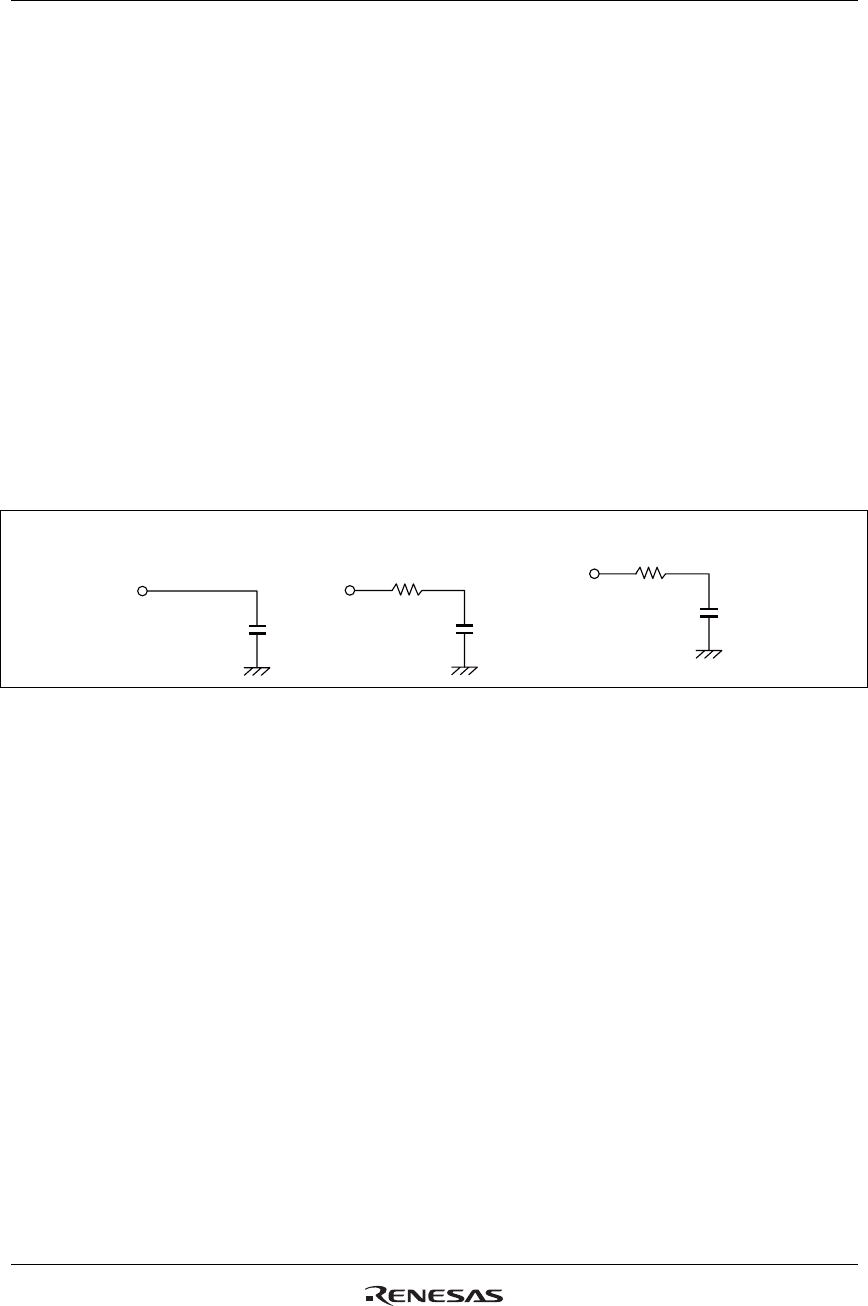
R61509V Target Spec
Rev. 0.11 April 25, 2008, page 176 of 181
Note 3: Test 1, 2 and 3 pins must be grounded. The VDDTEST and VREFC must be fixed to AGND. The
IM0_ID pin must be fixed to IOVCC or be grounded.
Note 4: This excludes the current in the output drive MOS.
Note 5: This excludes the current in the input/output lines. Make sure that the input level is fixed because
through current will increase in the input circuit when the CMOS input level takes a middle range
level. The current consumption is unaffected by whether the CSX pin is high or low while not
accessing via interface pins.
Note 7: The output voltage deviation is the difference in the voltages from adjacent source pins for the
same display area. This value is shown for reference.
Note 8: The average output voltage dispersion is the variance source-output voltage of different chips of the
same product. The average source output voltage is measured for each chip with same display area.
Note 9: This applies to internal oscillators when using an internal RC oscillator.
Note 10: The liquid crystal driver output delay time depends on the load on the liquid crystal panel. Adjust
the frame frequency and the cycle per line by checking the quality of display on the actual panel in
use.
Test Circuits
<Test circuits for AC characteristics>
Test Point
Test Point
30pF
10kΩ
<Test circuit for VCOM output characteristics>
Test Point
10nF
[Data bus DB17-DB0]
50pF Load capacitance C
<Test circuit for LCD output characteristics>
[Liquid output: S1-S720]
Load resistance R
100Ω
Load capacitance C
Figure 78
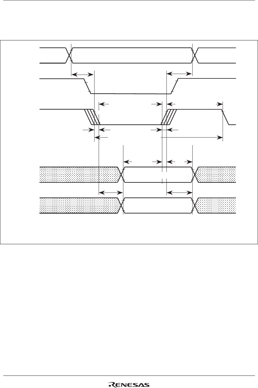
R61509V Target Spec
Rev. 0.11 April 25, 2008, page 177 of 181
Timing Characteristics
80-system Bus Interface
tDDR tDHR
VIL
VOL
tWRf
VIH
VIL
VIH
VIL
VIL
VIH
VIL
VIHVIH
VIL
VIH
RS
CSX
WRX
RDX
tAS tAH
PWHW PWHR
tWRr
tCYCW tCYCR
VIH
VIL
DB17-0
VIH
tDSW tH
VOH
VOL
DB17-0
VOH
PWLW PWLR
VIH
VIL
Note 2
Note 1
Write Data
Read Data
Note 1: PWLW and PWLR are defined by the overlap period when CSX is "Low" and either of WRX or RDX is "Low".
Note 2: Unused DB pins must be fixed at "IOVCC" or "GND".
Note 2
Figure A 80-system Bus Interface
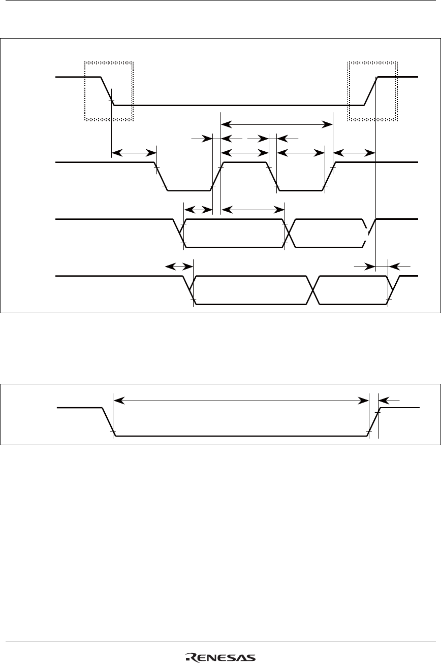
R61509V Target Spec
Rev. 0.11 April 25, 2008, page 178 of 181
Clock Synchronous Serial Interface
VILVIL
VIL
VIL
VIL
tsc
r
VIL
VIH
CSX
tSCYC
VIH
SCL
VIH
tCSU
SDI
VIH
VIH
VIL
VIH
tCH tSCH tSCL
tscf
VIH
tSISU tSISH
VOL1
SDO
VOH1
VOL1
VOH1
tSOD tSOH
Start: S End: P
Input Data Input Data
Output Data Output Data
Figure B Clock Synchronous Serial Interface Timing
Reset Operation
VIL
VIH
RESETX
tRES
VIL
trRES
Figure C Reset Timing
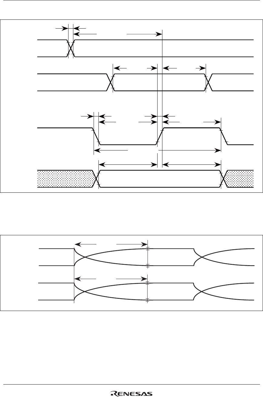
R61509V Target Spec
Rev. 0.11 April 25, 2008, page 179 of 181
RGB Interface
tPDH
VIL
VIH
VIL
VIH
VIL
VIL
VSYNCX
HSYNCX
VIH
VIH
VIL
ENABLE
VIH
tENS tENH
VIL
VIL
VIH
VIL
DOTCLK
VIH
PWDL PWDH
VIH
VIL
DB17-0
VIH
tPDS
tSYNCS
tCYCD
trgbf
trgbr
tr
g
bf tr
g
b
r
Write Data
Figure D RGB Interface Timing
LCD Driver and VCOM Output Characteristics
VCOM
S1-720
tDDs
tDDv
Target voltage r35mV
Target voltage r35mV
Target voltage r35mV
Target voltage r35mV
Figure E LCD Driver and VCOM Output Timing

Keep safety rst in your circuit designs!
1. Renesas Technology Corp. puts the maximum eort into making semiconductor products better and more reliable, but there is always the possibility that trouble may occur
with them. Trouble with semiconductors may lead to personal injury, re or property damage.
Remember to give due consideration to safety when making your circuit designs, with appropriate measures such as (i) placement of substitutive, auxiliary
circuits, (ii) use of nonammable material or (iii) prevention against any malfunction or mishap.
Notes:
1. This document is provided for reference purposes only so that Renesas customers may select the appropriate Renesas products for their use. Renesas neither makes
warranties or representations with respect to the accuracy or completeness of the information contained in this document nor grants any license to any intellectual property
rights or any other rights of Renesas or any third party with respect to the information in this document.
2. Renesas shall have no liability for damages or infringement of any intellectual property or other rights arising out of the use of any information in this document, including,
but not limited to, product data, diagrams, charts, programs, algorithms, and application circuit examples.
3. You should not use the products or the technology described in this document for the purpose of military applications such as the development of weapons of mass
destruction or for the purpose of any other military use. When exporting the products or technology described herein, you should follow the applicable export control laws
and regulations, and procedures required by such laws and regulations.
4. All information included in this document such as product data, diagrams, charts, programs, algorithms, and application circuit examples, is current as of the date this
document is issued. Such information, however, is subject to change without any prior notice. Before purchasing or using any Renesas products listed in this document,
please conrm the latest product information with a Renesas sales oce. Also, please pay regular and careful attention to additional and dierent information to be
disclosed by Renesas such as that disclosed through our website. (http://www.renesas.com)
5. Renesas has used reasonable care in compiling the information included in this document, but Renesas assumes no liability whatsover for any damages incurred as a result of
errors or omissions in the information included in this document.
6. When using or otherwise relying on the information in this document, you should evaluate the information in light of the total system before deciding about the applicability
of such information to the intended application. Renesas makes no representations, warranties or guarantees regarding the suitability of its products for any particular
application and specically disclaims any liability arising out of the application and use of the information in this document or Renesas products.
7. With the exception of products specied by Renesas as suitable for automobile applications, Renesas products are not designed, manufactured or tested for applications or
otherwise in systems the failure or malfunction of which may cause a direct threat to human life or create a risk of human injury or which require especially high quality and
reliability such as safety systems, or equipment or systems for transportation and trac, healthcare, combustion control, aerospace and aeronautics, nuclear power, or
undersea communication transmission. If you are considering the use of our products for such purposes, please contact a Renesas sales oce beforehand. Renesas shall
have no liability for damages arising out of the uses set forth above.
8. Notwithstanding the preceding paragraph, you should not use Renesas products for the purposes listed below:
(1) articial life support devices or systems
(2) surgical implantations
(3) healthcare intervention (e.g., excision, administration of medication, etc.)
(4) any other purposes that pose a direct threat to human life
Renesas shall have no liability for damages arising out of the uses set forth in the above and purchasers who elect to use Renesas products in any of the foregoing
applications shall indemnify and hold harmless Renesas Technology Corp., its aliated companies and their ociers, directors, and employees against any and all damages
arising out of such applications.
9. You should use the products described herein within the range specied by Renesas, especially with respect to the maximum rating, operating supply voltage range,
movement power voltage range, heat radiation characteristics, installation and other product characteristics. Renesas shall have no liability for malfunctions or damages
arising out of the use of Renesas products beyond such specied ranges.
10. Although Renesas endeavors to improve the quality and reliability of its products, IC products have specic characteristics such as the occurrence of failure at a certain
rate and malfunctions under certain use conditions. Please be sure to implement safety measures to guard against the possibility of physical injury, and injury or damage
caused by re in the event of the failure of a Renesas product, such as safety design for hardware and software including but not limited to redundancy, re control and
malfunction prevention, appropriate treatment for aging degradation or any other applicable measures. Among others, since the evaluation of microcomputer software
alone is very dicult, please evaluate the safety of the nal products or system manufactured by you.
11. In case Renesas products listed in this document are detached from the products to which the Renesas products are attached or axed, the risk of accident such as
swallowing by infants and small children is very high. You should implement safety measures so that Renesas products may not be easily detached from your products.
Renesas shall have no liability for damages arising out of such detachment.
12. This document may not be reproduced or duplicated, in any form, in whole or in part, without prior written approval from Renesas.
13. Please contact a Renesas sales oce if you have any questions regarding the information contained in this document, Renesas semiconductor products, or if you have any
other inquiries.
Sales Strategic Planning Div. Nippon Bldg., 2-6-2, Ohte-machi, Chiyoda-ku, Tokyo 100-0004, Japan
http://www.renesas.com
Renesas Technology America, Inc.
450 Holger Way, San Jose, CA 95134-1368, U.S.A
Tel: <1> (408) 382-7500 Fax: <1> (408) 382-7501
Renesas Technology Europe Limited.
Dukes Meadow, Millboard Road, Bourne End, Buckinghamshire, SL8 5FH, United Kingdom
Tel: <44> (1628) 585 100, Fax: <44> (1628) 585 900
Renesas Technology Europe GmbH
Dornacher Str. 3, D-85622 Feldkirchen, Germany
Tel: <49> (89) 380 70 0, Fax: <49> (89) 929 30 11
Renesas Technology Hong Kong Ltd.
7/F., North Tower, World Finance Centre, Harbour City, Canton Road, Hong Kong
Tel: <852> 2265-6688, Fax: <852> 2375-6836
Renesas Technology Taiwan Co., Ltd.
FL 10, #99, Fu-Hsing N. Rd., Taipei, Taiwan
Tel: <886> (2) 2715-2888, Fax: <886> (2) 2713-2999
Renesas Technology (Shanghai) Co., Ltd.
26/F., Ruijin Building, No.205 Maoming Road (S), Shanghai 200020, China
Tel: <86> (21) 6472-1001, Fax: <86> (21) 6415-2952
Renesas Technology Singapore Pte. Ltd.
1, Harbour Front Avenue, #06-10, Keppel Bay Tower, Singapore 098632
Tel: <65> 6213-0200, Fax: <65> 6278-8001
RENESAS SALES OFFICES
© 2008. Renesas Technology Corp., All rights reserved. Printed in Japan.
Colophon .1.0

R61509V Target Spec
Rev. 0.11 April 25, 2008, page 181 of 181
Revision Record
Rev. Date Page No. Contents of Modification Drawn
by
Approved by
0.11 2008/04/25 First issue
