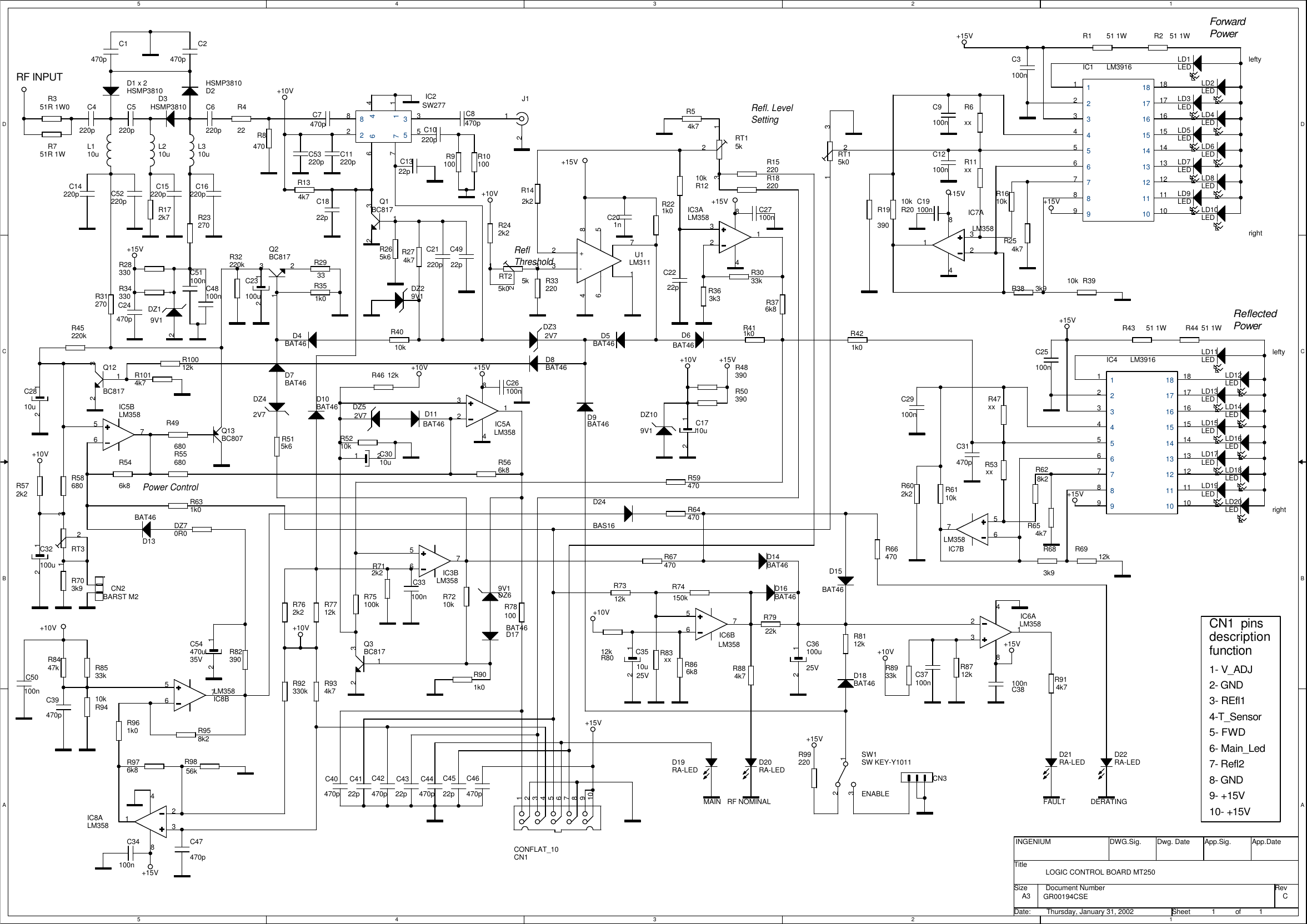
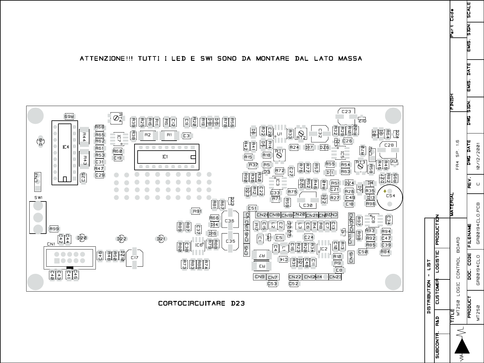
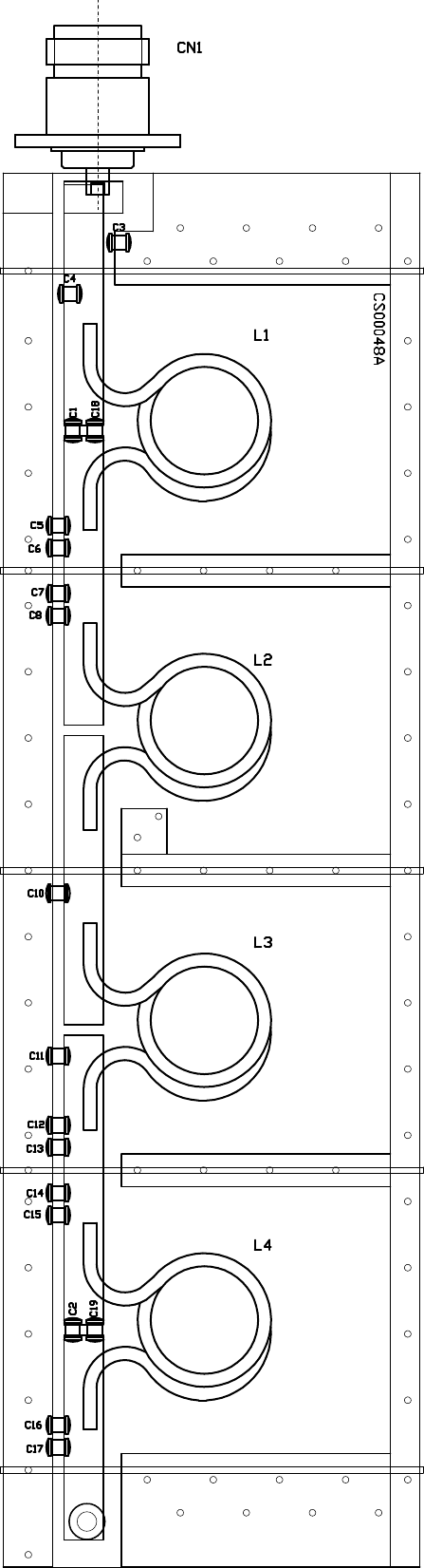
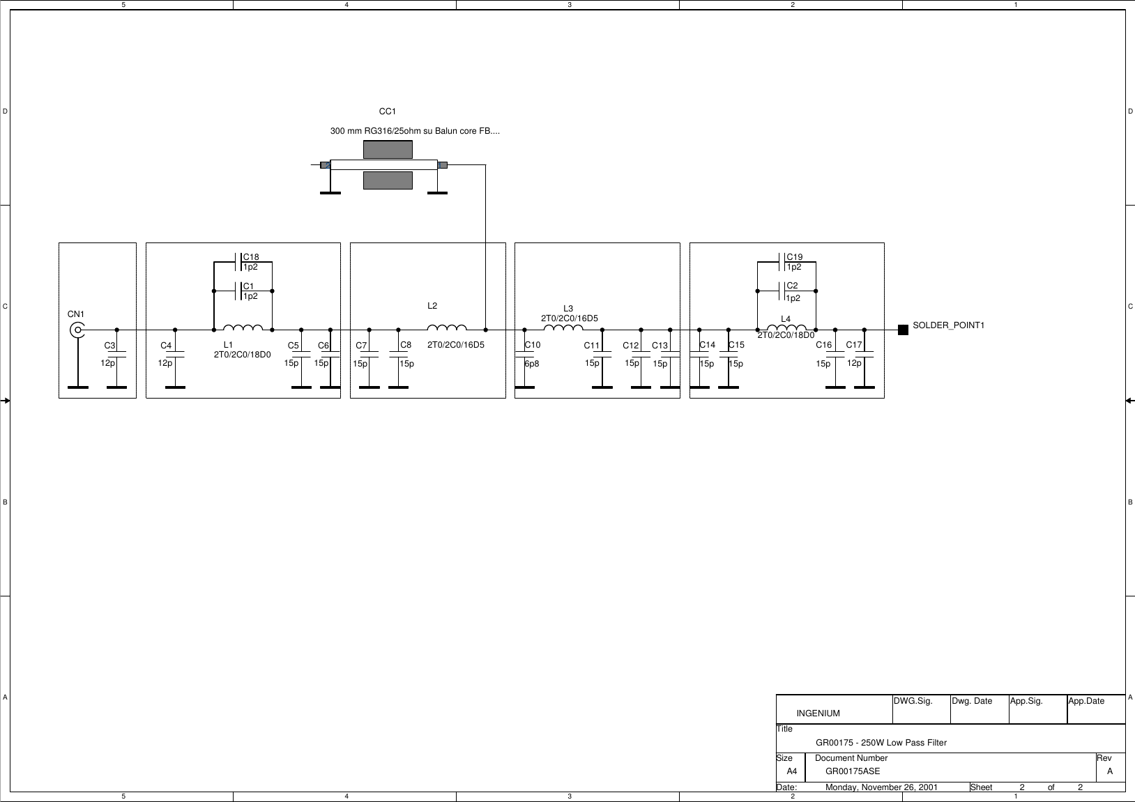
Richardson Electronics MT250 Low Power FM Transmitter User Manual Pages 1 to 13
Richardson Electronics Ltd Low Power FM Transmitter Pages 1 to 13
UserManual.wiki
>
Richardson Electronics
>
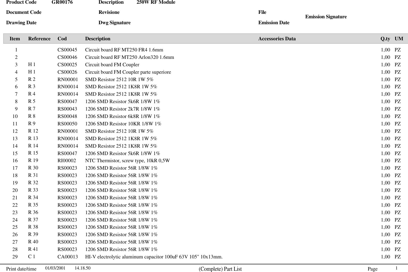
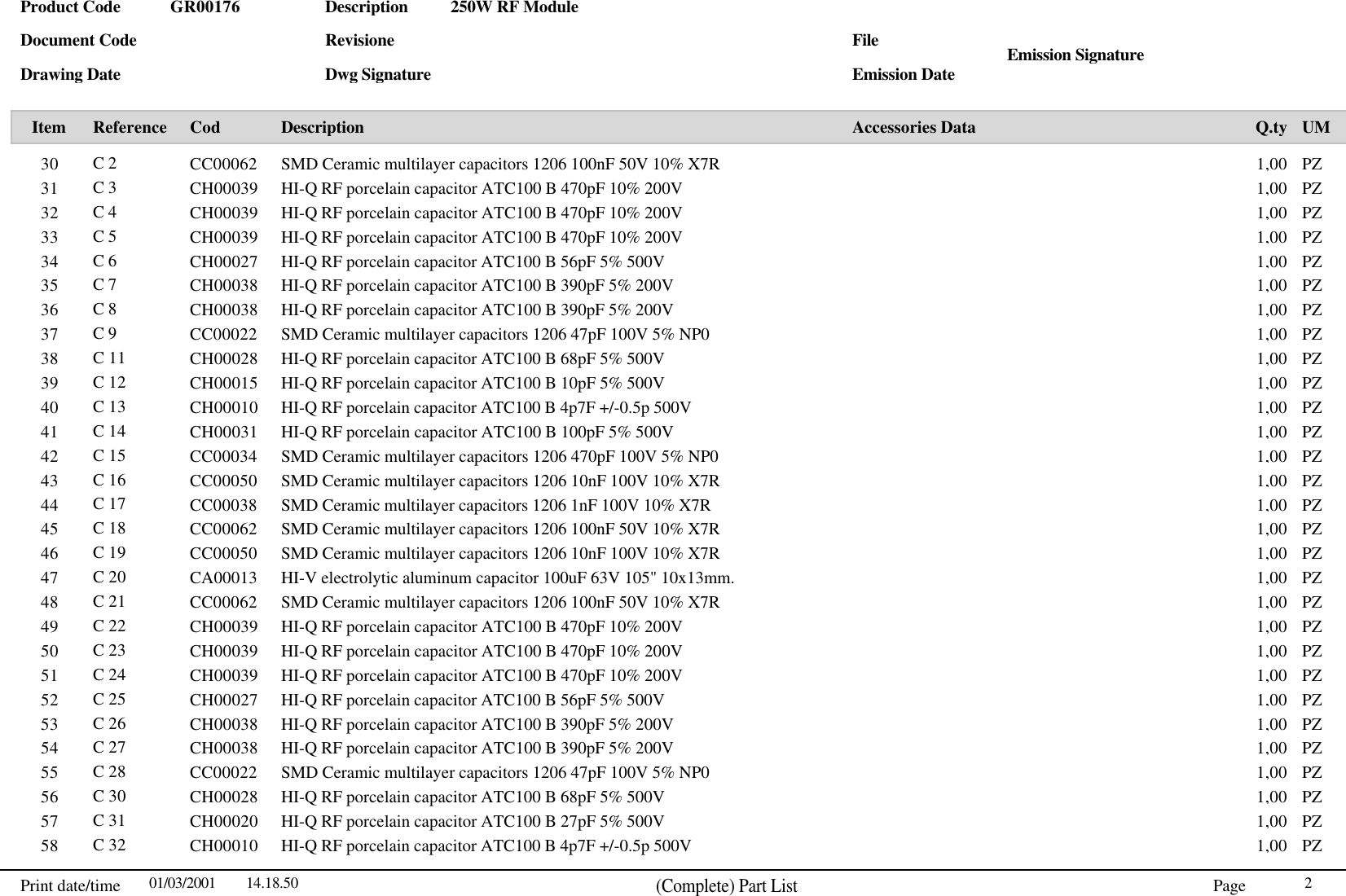
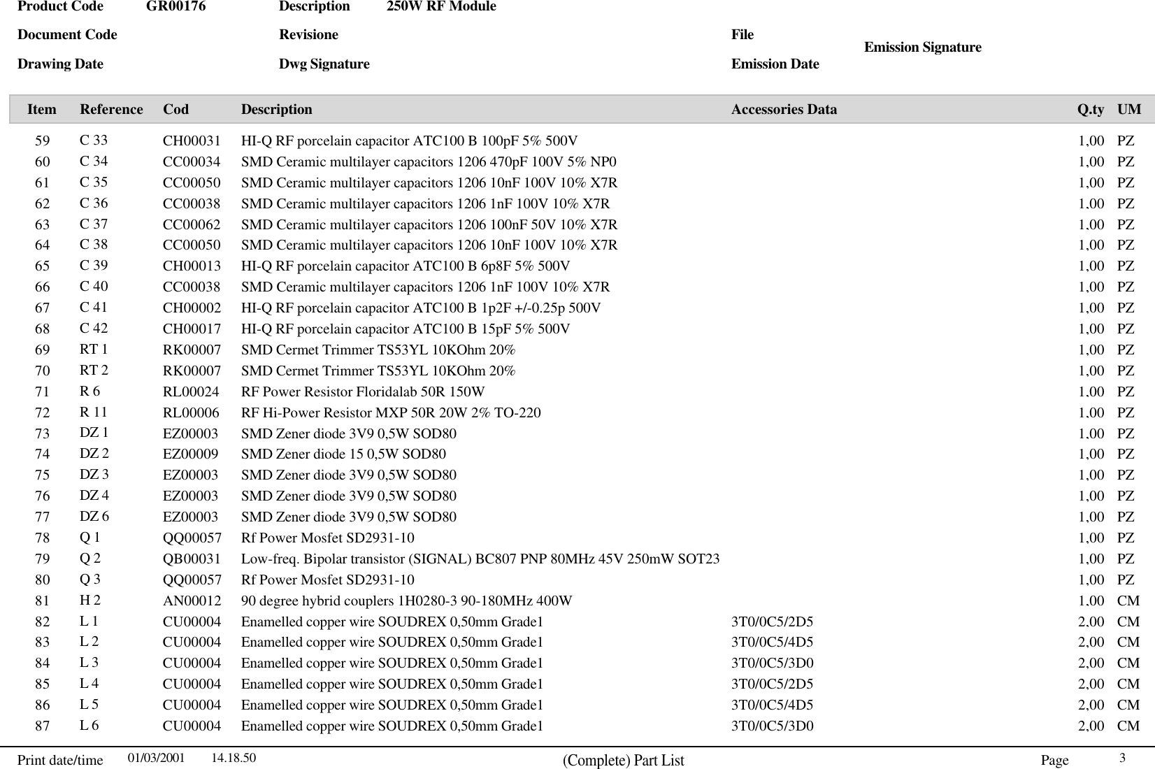
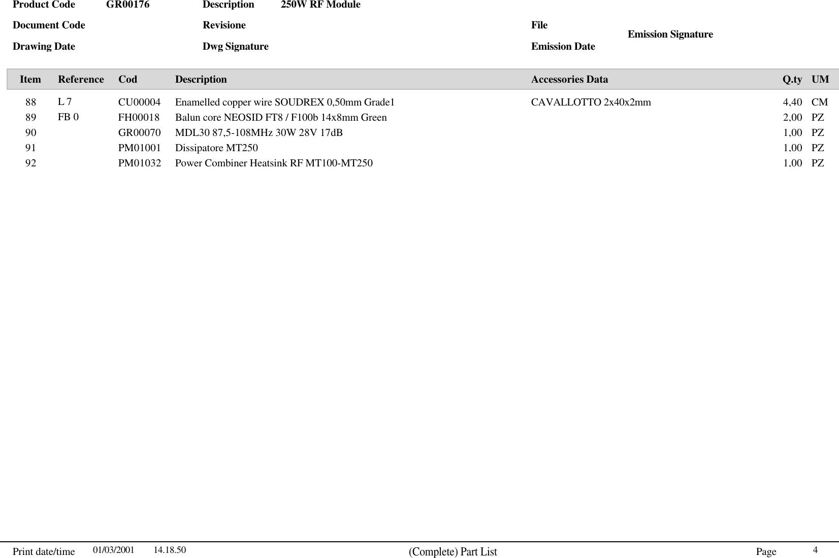
MT250 User Manual
Exhibit D Users Manual per 2 1033 c3
Navigation menu
Upload a User Manual
Namespaces
Wiki Guide
HTML
PDF
Info
Views
User Manual
Discussion / Help
Navigation