Rimage RFID1 13.56 MHz RFID Transceiver User Manual statement
Rimage Corporation 13.56 MHz RFID Transceiver statement
UserManual.wiki
>
Rimage
>
RFID1 User Manual
manual
Navigation menu
Upload a User Manual
Namespaces
Wiki Guide
HTML
PDF
Info
Views
User Manual
Discussion / Help
Navigation

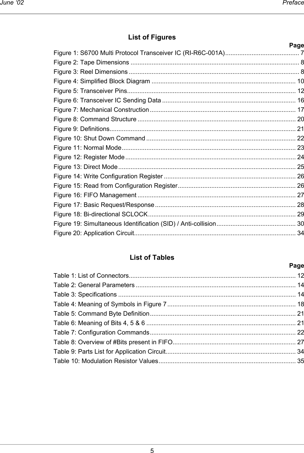
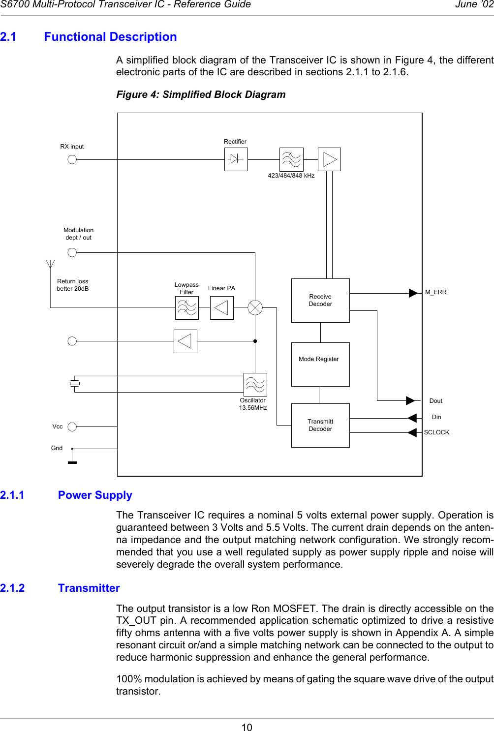
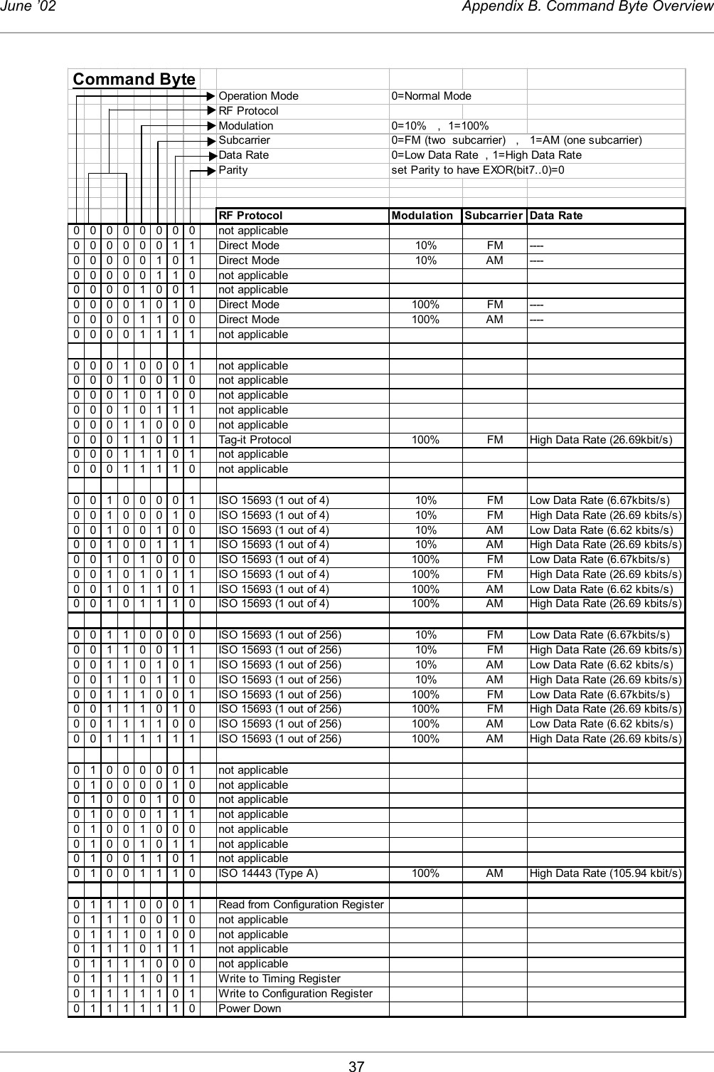
![7June ’02 Chapter 1. Introduction1.1 GeneralThis document provides information about the S6700 Multi Protocol Transceiver IC.It describes the integrated circuit and how to implement it. 1.2 System DescriptionThe HF Reader System Series 6000 works at a frequency of 13.56 MHz. It comprisesa reader, antenna and transponder (for example: smart label) and is used for wire-less identification.The system works according the “reader talks first” principle which means that thetransponder keeps quiet until the reader sends a request to it. The reader can rapidlyand simultaneously identify numerous transponders in the antenna’s field. It canwrite data to and read data from the transponders; either in addressed mode by usingthe factory programmed read only number, or in general mode to all of the transpond-ers in its field. The read/write capability of the transponder allows users to update thedata stored in the transponders memory anywhere along its movements. 1.3 Product DescriptionThe S6700 Multi Protocol Transceiver IC opens a rapid path for the development ofa broad range of 13.56 MHz RFID readers. It provides the receive/transmit functionsrequired to communicate with a variety of transponders that operate in the 13.56MHz ISM band. A transmit encoder converts the transmitted data stream into the se-lected protocol; protocol selection is done in the header of the transmitted data string.The transmitter can provide up to 200 mW of RF power to a matched 50 Ω load witha 5 V power supply. Higher output power can be obtained by an external amplifier. The receive decoder converts the signals from the RF receiver into a simple datastring. The digital interface provides on-chip data encoding and recovery, thereby minimiz-ing the software design efforts for the end user. Communication with the circuit isachieved by means of a three wire serial link. Figure 1: S6700 Multi Protocol Transceiver IC (RI-R6C-001A)1.4 Communications ProtocolsThe Transceiver IC can handle different RF protocols as follows: 1. Tag-it protocol. 2. ISO / IEC 15693-2 [2].3. ISO / IEC 14443-2 (Type A). 4. Direct mode where data can be passed directly thru to a transponder; using the correct modulation, timing, and command structure.](https://usermanual.wiki/Rimage/RFID1/User-Guide-303849-Page-9.png)