Rimage RFID1 13.56 MHz RFID Transceiver User Manual statement
Rimage Corporation 13.56 MHz RFID Transceiver statement
Rimage >
manual
1. Instruction Manual
The RFID1 is designed for use by Original Equipment Manufacturers (OEM) for inclusion into their products. There are no
end user instructions necessary for use or maintenance. See the following pages for the integration and usage
instructions.
FCC ID: QT5-RFID1

OFFICE CORRESPONDENCE
7725 Washington Ave. South; Minneapolis, Minnesota 55349 USA Phone: (952) 944-8144 Fax: (952) 944-7808
OEM Integration Instructions for Rimage P/N 626371-001, FCC ID: QT5-RFID1
File: RFID1 OEM.doc, 06-Feb-03 Phil Salisbury Page 1 of
1
CONFIDENTIAL, not to be released without written authorization from Rimage Corporation.
1. General
The RFID1 device is used by Original Equipment Manufacturers (OEM) to integrate close range (2-inch or less) ISO 15693
transponder communications into a product. There are no usage, calibration, or maintenance instructions necessary for the
end user. There are no calibrations necessary for the OEM. There are no special accessories required for either the OEM or
end user.
2. Identification Nameplate Requirements
The following information must be included as part of the permanent and end user visible equipment identification
nameplate. These markings may only be applied after the OEM has tested to ensure compliance with the relevant national
standards.
!
This device contains a radio transmitter FCC ID: QT5-RFID1; IC: 4496A-RFID1.
This device complies with part 15 of the FCC Rules. Operation is subject to the following two
conditions: (1) This device may not cause harmful interference, and (2) this device must accept
any interference received, including interference that may cause undesired operation.
3. Compliance Statement Requirements for User Documentation.
The following information must be included in the end user documentation provided by the OEM.
4. Transceiver Control
The RFID1 is based on the Texas Instruments RI-R6C-001A transceiver integrated circuit (IC). Control of this IC is
specified in Texas Instruments document 11-07-21-001+S6700+Reference+Guide+V3.pdf. Rimage has developed
controlling firmware and will work with the OEM to integrate that control into their product. The Rimage firmware sets up
the IC and manages data communications between the IC and the transponder.
Notice for the USA
This device contains a radio transmitter FCC ID: QT5-RFID1. This device complies with part 15 of the
FCC Rules. Operation is subject to the following two conditions: (1) This device may not cause harmful
interference, and (2) this device must accept any interference received, including interference that may
cause undesired operation. Any unauthorized modification to this equipment may result in the revocation
by the FCC of the user’s authority to operate this equipment.
Notice for Canada
This product contains a radio transmitter IC: 4496A-RFID1 in conformance with RSS-210: Issue 5: 2001.
The term “IC” before the radio certification number only signifies that Industry Canada Technical
specifications were met.
Notice for Europe
!
This product contains a radio transmitter (RFID1) in conformity with R&TTE directive
1999/5/EC through compliance with the following European Standards:
EN 300 330-2 v1.1.1: 2001; EN 301 489-3:2002 Class B Limit.

1
June ’02 Appendix C. Register Definition
11-07-21-001 June 2002
HF Reader System Series 6000
S6700 Multi Protocol Transceiver IC
RI-R6C-001A
Reference Guide
A TEXAS INSTRUMENTS TECHNOLOGY

2
S6700 Multi-Protocol Transceiver IC - Reference Guide June ’02
Edition Three - June 2002
This is the third edition of this manual. It describes the following product:
S6700 Multi Protocol Transceiver IC RI-R6C-001A-02
Texas Instruments (TI) reserves the right to make changes to its products or services
or to discontinue any product or service at any time without notice. TI provides cus-
tomer assistance in various technical areas, but does not have full access to data
concerning the use and applications of customer's products.
Therefore, TI assumes no liability and is not responsible for customer applications or
product or software design or performance relating to systems or applications incor-
porating TI products. In addition, TI assumes no liability and is not responsible for
infringement of patents and/or any other intellectual or industrial property rights of
third parties, which may result from assistance provided by TI.
TI products are not designed, intended, authorized or warranted to be suitable for life
support applications or any other life critical applications which could involve poten-
tial risk of death, personal injury or severe property or environmental damage.
The TIRIS and TI-RFID logos, the words TIRIS, TI-RFID and Tag-it are trademarks
or registered trademarks of Texas Instruments Incorporated.
Copyright 2002 Texas Instruments Incorporated (TI)
This document may be downloaded onto a computer, stored and duplicated as nec-
essary to support the use of the related TI products. Any other type of duplication,
circulation or storage on data carriers in any manner not authorised by TI represents
a violation of the applicable copyright laws and shall be prosecuted.
3
June ‘02 Preface
About This Manual
This reference guide for the S6700 Multi Protocol Transceiver IC is designed for use
by TI partners who are engineers experienced with Radio Frequency Identification
Devices (RFID).
Regulatory, safety and warranty notices that must be followed are given in
Chapter 5.
Conventions
If You Need Assistance
For more information, please contact the sales office or distributor nearest you. This
contact information can be found on our web site at:
http://www.ti-rfid.com
WARNING:
A WARNING IS USED WHERE CARE MUST BE TAKEN, OR A
CERTAIN PROCEDURE MUST BE FOLLOWED IN ORDER TO PRE-
VENT INJURY OR HARM TO YOUR HEALTH.
CAUTION:
This indicates information on conditions which must be
met, or a procedure which must be followed, which if not
heeded could cause permanent damage to the equipment
or software.
Note:
Indicates conditions which must be met, or procedures which must be
followed, to ensure proper functioning of the equipment or software.
Information:
Indicates information which makes usage of the equipment or soft-
ware easier

4
S6700 Multi-Protocol Transceiver IC - Reference Guide June ’02
Document Overview
Page
Chapter 1: Introduction. . . . . . . . . . . . . . . . . . . . . . . . . . . . . . . . . . . . . . . . . . . . . . . . . . . . . . . . . . . . 6
1.1 General .................................................................................................................... 7
1.2 System Description .................................................................................................. 7
1.3 Product Description .................................................................................................. 7
1.4 Communications Protocols....................................................................................... 7
1.5 Delivery .................................................................................................................... 8
Chapter 2: Transceiver IC Description . . . . . . . . . . . . . . . . . . . . . . . . . . . . . . . . . . . . . . . . . . . . . . . 9
2.1 Functional Description............................................................................................ 10
2.2 Pin Description ....................................................................................................... 12
Chapter 3: Technical Data . . . . . . . . . . . . . . . . . . . . . . . . . . . . . . . . . . . . . . . . . . . . . . . . . . . . . . . . 13
3.1 Specification Summary........................................................................................... 14
3.2 Mechanical Information .......................................................................................... 17
Chapter 4: Protocol Definition . . . . . . . . . . . . . . . . . . . . . . . . . . . . . . . . . . . . . . . . . . . . . . . . . . . . . 19
4.1 General Remarks and Basic Command Structure ................................................. 20
4.2 Operating Modes.................................................................................................... 23
4.3 RF Protocol ............................................................................................................ 25
4.4 Register Configuration............................................................................................ 26
4.5 Communication ...................................................................................................... 27
4.6 Power Management ............................................................................................... 31
4.7 Pin M_ERR ............................................................................................................ 31
Chapter 5: Regulatory, Safety and Warranty Notices . . . . . . . . . . . . . . . . . . . . . . . . . . . . . . . . . . 32
5.1 Regulatory Notes ................................................................................................... 33
Appendix A: Application Examples . . . . . . . . . . . . . . . . . . . . . . . . . . . . . . . . . . . . . . . . . . . . . . . . . . 34
Appendix B: Command Byte Overview . . . . . . . . . . . . . . . . . . . . . . . . . . . . . . . . . . . . . . . . . . . . . . . 36
Appendix C: Register Definition . . . . . . . . . . . . . . . . . . . . . . . . . . . . . . . . . . . . . . . . . . . . . . . . . . . . . 38
Appendix D: Terms & Abbreviations . . . . . . . . . . . . . . . . . . . . . . . . . . . . . . . . . . . . . . . . . . . . . . . . . 41

5
June ‘02 Preface
List of Figures
Page
Figure 1: S6700 Multi Protocol Transceiver IC (RI-R6C-001A).......................................... 7
Figure 2: Tape Dimensions ................................................................................................ 8
Figure 3: Reel Dimensions ................................................................................................. 8
Figure 4: Simplified Block Diagram .................................................................................. 10
Figure 5: Transceiver Pins................................................................................................ 12
Figure 6: Transceiver IC Sending Data ............................................................................ 16
Figure 7: Mechanical Construction ................................................................................... 17
Figure 8: Command Structure .......................................................................................... 20
Figure 9: Definitions.......................................................................................................... 21
Figure 10: Shut Down Command ..................................................................................... 22
Figure 11: Normal Mode................................................................................................... 23
Figure 12: Register Mode ................................................................................................. 24
Figure 13: Direct Mode ..................................................................................................... 25
Figure 14: Write Configuration Register ........................................................................... 26
Figure 15: Read from Configuration Register................................................................... 26
Figure 16: FIFO Management .......................................................................................... 27
Figure 17: Basic Request/Response ................................................................................ 28
Figure 18: Bi-directional SCLOCK.................................................................................... 29
Figure 19: Simultaneous Identification (SID) / Anti-collision............................................. 30
Figure 20: Application Circuit............................................................................................ 34
List of Tables
Page
Table 1: List of Connectors............................................................................................... 12
Table 2: General Parameters ........................................................................................... 14
Table 3: Specifications ..................................................................................................... 14
Table 4: Meaning of Symbols in Figure 7 ......................................................................... 18
Table 5: Command Byte Definition................................................................................... 21
Table 6: Meaning of Bits 4, 5 & 6 ..................................................................................... 21
Table 7: Configuration Commands................................................................................... 22
Table 8: Overview of #Bits present in FIFO...................................................................... 27
Table 9: Parts List for Application Circuit.......................................................................... 34
Table 10: Modulation Resistor Values.............................................................................. 35

CHAPTER 1
6
Introduction
Chapter 1:Introduction
This chapter introduces you to the S6700 Multi Protocol Transceiver IC.
Topic Page
1.1 General........................................................................................................7
1.2 System Description....................................................................................7
1.3 Product Description...................................................................................7
1.4 Communications Protocols ......................................................................7
1.5 Delivery .......................................................................................................8
7
June ’02 Chapter 1. Introduction
1.1 General
This document provides information about the S6700 Multi Protocol Transceiver IC.
It describes the integrated circuit and how to implement it.
1.2 System Description
The HF Reader System Series 6000 works at a frequency of 13.56 MHz. It comprises
a reader, antenna and transponder (for example: smart label) and is used for wire-
less identification.
The system works according the “reader talks first” principle which means that the
transponder keeps quiet until the reader sends a request to it. The reader can rapidly
and simultaneously identify numerous transponders in the antenna’s field. It can
write data to and read data from the transponders; either in addressed mode by using
the factory programmed read only number, or in general mode to all of the transpond-
ers in its field. The read/write capability of the transponder allows users to update the
data stored in the transponders memory anywhere along its movements.
1.3 Product Description
The S6700 Multi Protocol Transceiver IC opens a rapid path for the development of
a broad range of 13.56 MHz RFID readers. It provides the receive/transmit functions
required to communicate with a variety of transponders that operate in the 13.56
MHz ISM band. A transmit encoder converts the transmitted data stream into the se-
lected protocol; protocol selection is done in the header of the transmitted data string.
The transmitter can provide up to 200 mW of RF power to a matched 50 Ω load with
a 5 V power supply. Higher output power can be obtained by an external amplifier.
The receive decoder converts the signals from the RF receiver into a simple data
string.
The digital interface provides on-chip data encoding and recovery, thereby minimiz-
ing the software design efforts for the end user. Communication with the circuit is
achieved by means of a three wire serial link.
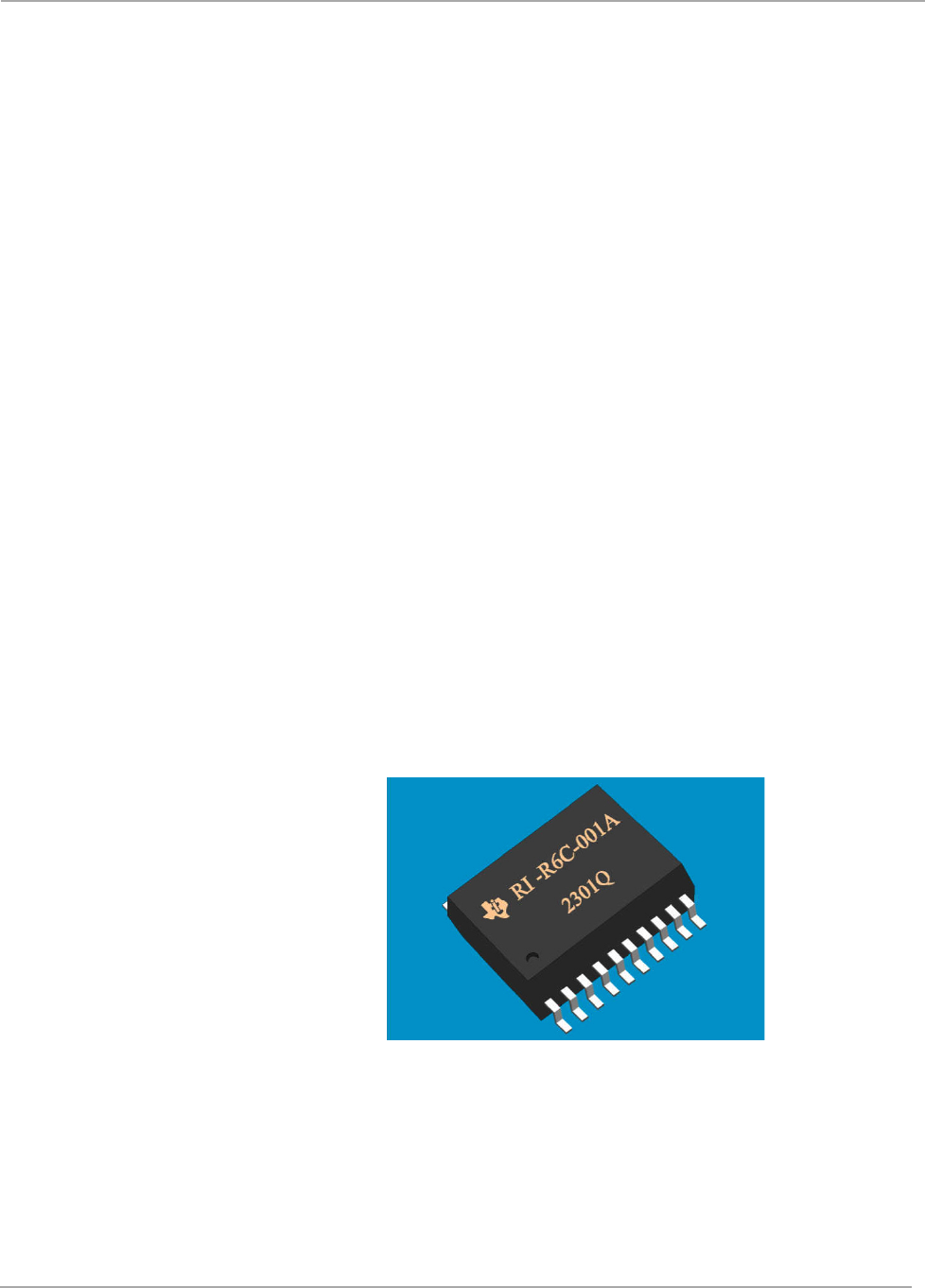
Figure 1: S6700 Multi Protocol Transceiver IC (RI-R6C-001A)
1.4 Communications Protocols
The Transceiver IC can handle different RF protocols as follows:
1. Tag-it protocol.
2. ISO / IEC 15693-2 [2].
3. ISO / IEC 14443-2 (Type A).
4. Direct mode where data can be passed directly thru to a transponder; using the
correct modulation, timing, and command structure.
8
S6700 Multi-Protocol Transceiver IC - Reference Guide June ’02
1.5 Delivery
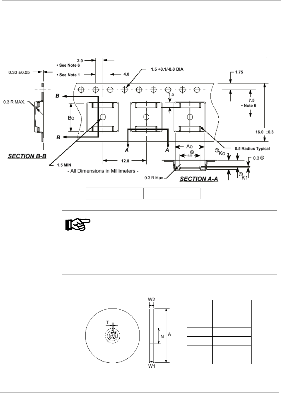
The Transceiver IC is available in an SSOP20 plastic package and will be delivered
in quantities of 1500 units packed tape-on-reel. The dimensions for the carrier tape
and reel are shown on Figure 2 and Figure 3.
Figure 2: Tape Dimensions
Figure 3: Reel Dimensions
A0 = 8.2 K1 = 2.3 K0 = 3.0 B0 = 7.6
Notes:
1) 10 sprocket hole pitch cumulative tolerance ± 0.2 mm.
2) Camber not to exceed 1 mm in 100 mm.
3) Material: Black Conductive Polystyrene.
4) Ao and Bo measured on a plane 0.3 mm above the bottom of the pocket.
5) Ko measured from a plane on the inside bottom of the pocket to the top
surface of the carrier.
6) Pocket position relative to sprocket hole measured as true position of
pocket, not pocket hole.
A 330.0 mm
N 102.0 mm
D 13.0 mm
R 10.1 mm
T 2.0 mm
W1 16.8 mm
W2 22.2 mm

CHAPTER 2
9
Transceiver IC Description
Chapter 2:Transceiver IC Description
This chapter describes the hardware of the S6700 Transceiver IC. It describes the
transceiver’s functionality and its interfaces.
Topic Page
2.1 Functional Description ............................................................................10
2.1.1 Power Supply .......................................................................................10
2.1.2 Transmitter ...........................................................................................10
2.1.3 Receiver ...............................................................................................11
2.1.4 Reference Clock and Internal Oscillator...............................................11
2.1.5 Reset Defaults and Power Management .............................................11
2.1.6 Serial communication interface ............................................................11
2.2 Pin Description.........................................................................................12
10
S6700 Multi-Protocol Transceiver IC - Reference Guide June ’02
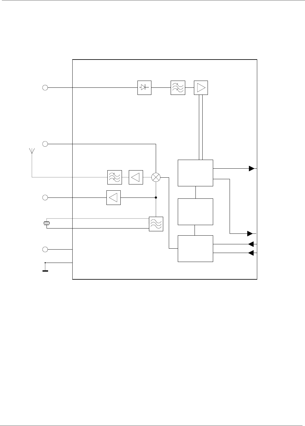
2.1 Functional Description
A simplified block diagram of the Transceiver IC is shown in Figure 4, the different
electronic parts of the IC are described in sections 2.1.1 to 2.1.6.
Figure 4: Simplified Block Diagram
2.1.1 Power Supply
The Transceiver IC requires a nominal 5 volts external power supply. Operation is
guaranteed between 3 Volts and 5.5 Volts. The current drain depends on the anten-
na impedance and the output matching network configuration. We strongly recom-
mended that you use a well regulated supply as power supply ripple and noise will
severely degrade the overall system performance.
2.1.2 Transmitter
The output transistor is a low Ron MOSFET. The drain is directly accessible on the
TX_OUT pin. A recommended application schematic optimized to drive a resistive
fifty ohms antenna with a five volts power supply is shown in Appendix A. A simple
resonant circuit or/and a simple matching network can be connected to the output to
reduce harmonic suppression and enhance the general performance.
100% modulation is achieved by means of gating the square wave drive of the output
transistor.
423/484/848 kHz
Linear PA
Lowpass
Filter
Din
Dout
SCLOCK
Transmitt
Decoder
Mode Register
Modulation
dept / out
Return loss
better 20dB
Receive
Decoder
Oscillator
13.56MHz
RX input
Vcc
Gnd
M_ERR
Rectifier

11
June ’02 Chapter 2. Transceiver IC Description
The ten percent modulation depth is obtained by means of switching a resistor in se-
ries with the output transistor source connection. Increasing the value of this resistor
further increases the modulation depth.
The transmit encoder converts the data into the selected RF Protocol to be trans-
ferred. The communications speed varies from 5 to 120 kbaud and must be at least
the speed of the selected transponder protocol. An input buffer is implemented in or-
der to have a sufficient number of bits available for the RF transmission.
2.1.3 Receiver
The receiver input is typically connected to the antenna through an external resistor.
The modulation from the tag is then recovered by means of a diode envelope detec-
tor.
The receiver decoder issues the received data directly to the controller in binary data
format. The communication speed and RF protocol is defined by the selected mode.
Start, stop and errors in the received data string are detected and indicated at the
output.
2.1.4 Reference Clock and Internal Oscillator
The reference clock can be obtained externally by applying a suitable clock signal to
the XTAL2 pin. A sine wave centered at VCC/2 or a CMOS logic compatible signal
is an acceptable external system clock. The built-in reference oscillator will work ei-
ther with a quartz crystal or a ceramic resonator. The nominal system clock frequen-
cy is 13.56 MHz, but the oscillator will work at any frequency from 4 MHz to 16 MHz.
A buffered version of the crystal oscillator signal is available for synchronization pur-
poses on pin 8 (XTAL_CLOCK).
2.1.5 Reset Defaults and Power Management
After a power on reset has been performed, the device is placed in its default config-
uration. There are three available power modes. In the first mode, the device is fully
powered. In the idle mode, only the reference oscillator and a minimal set of associ-
ated circuitry are running. In the power down mode, the device internal bias system
is completely switched off. The circuit is woken by applying a rising edge on the DIN
line while SCLOCK is held high.
2.1.6 Serial communication interface
The communication interface normally uses three wires:
SCLOCK, serial clock, bi-directional.
DIN, data input, as seen by the circuit
DOUT, data output, as seen by the circuit
The commands are sent with the most significant bit (MSB) in the first position. All
signals are internally synchronized with the system clock.
The bit protocol is fully described in Chapter 4.

12
S6700 Multi-Protocol Transceiver IC - Reference Guide June ’02
2.2 Pin Description
Figure 5 shows the Transceiver IC and the signals on each pin. They are further de-
scribed in Table 1.
Figure 5: Transceiver Pins
Table 1: List of Connectors
Pin
number Signal Name Description
1 VDD_TX Transmitter power supply
2 TX_OUT Output transistor drain connection
3 R_MOD External resistor to set 10% modulation depth mode
4 VSS_TX Transmitter section ground
5 XTAL1 Pin 1 of Xtal resonator
6 XTAL2 Pin 2 of Xtal resonator and external system clock input
7 VSS_DIG Digital section ground
8 XTAL_CLK Buffered output of Xtal oscillator
9 not used Grounded for normal operation
10 not used Grounded for normal operation
11 DOUT Data output for serial link
12 VDD_DIG Digital section power supply
13 DIN Data input for serial link
14 M_ERR Manchester Protocol error flag
15 SCLOCK Serial link clock
16 not used Leave open for normal operation
17 VDD_RX Receiver section power supply
18 not used Leave open for normal operation
19 VSS_RX Receiver section ground
20 RX_IN Receiver input
1 VDD_TX
2 TX_OUT
3 R_MOD
4 VSS_TX
5 XTAL1
6 XTAL2
7 VSS_DIG
8 XTAL_CLK
9
10
VSS_RX 19
RX_IN 20
VDD_RX 17
18
16
SCLOCK 15
M_ERR 14
DIN 13
VDD_DIG 12
DOUT 11

CHAPTER 3
13
Technical Data
Chapter 3:Technical Data
This chapter provides the technical specifications of the S6700 Transceiver IC. It also
provides information about packing and storage.
Topic Page
3.1 Specification Summary ...........................................................................14
3.2 Mechanical Information ...........................................................................17

14
S6700 Multi-Protocol Transceiver IC - Reference Guide June ’02
3.1 Specification Summary
These specifications apply under the following environmental conditions unless oth-
erwise stated:
Ambient temperature = -40 ºC to +85 ºC,
Input voltage = 5 Volts,
The on-board resonator was used.
Table 2: General Parameters
Parameter Condition Min Typ Max Unit
Interface Serial Interface, CMOS compatible
Package SSOP20
Lead frame material CDA C19400
Lead finish material Solder Plate 85/15 Sn/Pb
Operating temperature -40 +85 ºC
Storage temperature -55 +125 ºC
Power dissipation 500 mW
ESD protection MIL-STD-883, Method 3015 (2kV, 1.5 kΩ, 100 pF)
Table 3: Specifications
Parameter Condition Min Typ Max Unit
General DC Parameters:
Supply voltage (Vdd) Vdd with respect
to Vss 355.5Volt
Supply ripple See note 3 40 mVpp
Stand-by current consumption (Istb) Vdd=5.5 V - 1 50 µA
Idle mode current consumption (Idle1)
(Analog section off)
External clock
Vdd=5.5 V -1215mA
Idle mode current consumption (Idle2)
(Analog section off)
On board
resonator
Vdd=5.5 V
3711mA
Operating current (Iop) - 9 14 19 mA
Transmit current (Itr) See note 1 80 100 120 mA
Transmitter specifications:
Max peak voltage applied on drain of
output transistor ---32V
Max output transistor power dissipation - - - 500 mW
Output transistor ON resistance Id = 50 mA - 2 5 Ohm
Output power for five volts operation See note 1 180 200 - mW
Amplitude modulation depth adjustment
range in 10% mode, with external resistor
connected between R_MOD pin and
ground.
See note 1 0% - 90% -

15
June ’02 Chapter 3. Technical Data
Amplitude modulation depth in 10% mode
with 12 Ohm external resistor See note 1 10% 12% 16% -
Minimum depth for 100% ASK See note 1 40 - - dB
Rise and fall time for 100% ASK See note 1 - 2.5 4 µs
Rise and fall time for 10% modulation
depth (nominal external resistor used) See note 1 - 1 1.5 µs
Receiver specifications:
Input RF voltage range (RX_IN - VSS) With 1 k series
external resistor 1 1.8 - 4.9 Vdd Volt
Receiver sensitivity (FSK) See note 1 -40 -65 - dBm
Baseband receiver sensitivity (FSK) See note 1 -40 -65 - dBm
FSK IF filter cut off points 130 200-
1400 1800 kHz
Total gain, in FSK mode - 100 120 140 dB
Log amplifier section:
Limiting gain - 70 80 - dB
Sensitivity for AM recovery - -40 -55 - dBm
Sensitivity for FM recovery - -40 -65 - dBm
Serial Link and digital I/O:
Output voltage low (Vol) lmax=1mA 0 0.2 0.4 Volt
Output voltage high (Voh) 4.6 4.8 5 Volt
Output current drive (Iol) Vol ≤ 0.4 Volt 1 - - mA
Input voltage high (Vih) 0.7 Vdd - Vdd +
0.3 V
Input voltage low (Vil) -0.3 - 0.3
Vdd V
SCLOCK frequency See note 4 1.5 MHz
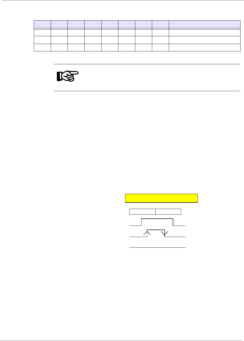
SCLOCK and DATA set up time See Figure 6 300 ns
Xtal Oscillator:
Frequency range (Fxtal) - 4 13.56 16 MHz
Start-up time (Tstart) - - 2 5 ms
Xtal series resistance 50 100 Ohm
External clock signal specifications: See note 2
Min sine wave amplitude AC coupled - 1 - Vdd Volt pp
Min sine wave amplitude, DC coupled
Input has to be
centered around
Vdd/2
1 - Vdd Volt pp
Table 3: Specifications
Parameter Condition Min Typ Max Unit
16
S6700 Multi-Protocol Transceiver IC - Reference Guide June ’02
Figure 6: Transceiver IC Sending Data
XTAL_CLK output specifications:
XTAL_CLK Low Level (Col) 1K load resistor 0 0.2 0.4 Volt
XTAL_CLK High Level (Coh) 1K load resistor 4.6 4.8 5.0 Volt
Rise and fall times (10%-90%) 1K load resistor//
12pF -3-ns
Notes:
1) This parameter is specified with the IC wired as shown in the
typical application circuit shown in Appendix A, with the trans-
mitter switched on.
2) The external clock symmetry is of paramount importance. It
has a direct influence on the transmitter output power. When
using a sine wave as an external clock input, it must not show
visible distortion. If a square wave is used, its duty cycle has to
be equal to 50%. In all cases, the resulting duty cycle should be
checked on the XTAL_CLK pin when it is configured as an out-
put.
3) The maximum ripple current could result in a 10% reduction of
the reading distance.
4) The minimum frequency must be high enough that the Trans-
ceiver IC always has data available to send.
Table 3: Specifications
Parameter Condition Min Typ Max Unit
Sclock
DOUT
T1
T1: typical 300ns
17
June ’02 Chapter 3. Technical Data
3.2 Mechanical Information
Figure 7: Mechanical Construction
See Table 4 on next page for details of the symbols in Figure 7.
18
S6700 Multi-Protocol Transceiver IC - Reference Guide June ’02
Table 4: Meaning of Symbols in Figure 7
Symbol Min. Nom. Max. See Note
A 1.73 1.86 1.99
A10.05 0.13 0.21
A21.68 1.73 1.78
b 0.25 - 0.38 8,10
b10.25 0.30 0.33 10
c 0.09 - 0.20 10
c1 0.09 0.15 0.16 10
D 7.07 7.20 7.33 4
E 5.20 5.30 5.38 4
e 0.65BSC
H 7.65 7.80 7.90
L 0.63 0.75 0.95 5
L1 1.25 Ref.
N20
α0° 4° 8°
R 0.09 0.15
Notes:
1) This package outline drawing complies with JEDEC Specifica-
tion No. MO-150.
2) Dimensions and Tolerances per ANSI.Y14.5M-1982.
3) "T" is a reference datum.
4) "D" & "E" are reference datums and do not include mold flash or
protrusions, but do include mold mismatch and are measured at
the parting line. Mold flash or protrusions shall not exceed 0.15
mm per side.
5) Dimension is the length of terminal for soldering to a substrate.
6) Terminal positions are shown for reference only.
7) Formed leads shall be planar with respect to one another within
0.08 mm at seating plane.
8) Dimension b does not include dambar protrusion/intrusion.
Allowable dambar protrusion shall be 0.13 mm total in excess of
b dimension at maximum material condition. Dambar intrusion
shall not reduce dimension b by more than 0.07 mm at least
material condition.
9) Controlling dimension: millimeters.
10) These dimensions apply to the flat section of the lead between
0.10 mm and 0.25 mm from lead tips.

CHAPTER 4
19
Protocol Definition
Chapter 4:Protocol Definition
This chapter provides information about the communication protocol used by the
S6700 Transceiver IC.
Topic Page
4.1 General Remarks and Basic Command Structure................................20
4.1.1 Definition of Start (S1), Stop (ES1) and Data bit..................................20
4.1.2 Command byte definition .....................................................................21
4.1.3 Transmitter Off Command....................................................................22
4.1.4 Transmitter On command ....................................................................22
4.2 Operating Modes......................................................................................23
4.2.1 Common Points (Normal and Register Mode) .....................................23
4.2.2 Normal Mode........................................................................................23
4.2.3 Register Mode......................................................................................24
4.3 RF Protocol...............................................................................................25
4.3.1 General ................................................................................................25
4.3.2 Direct Mode..........................................................................................25
4.4 Register Configuration ............................................................................26
4.4.1 Write Data to Configuration Register ...................................................26
4.4.2 Read Data from Configuration Register ...............................................26
4.5 Communication ........................................................................................ 27
4.5.1 FIFO Management ...............................................................................27
4.5.2 Basic Request/Response.....................................................................28
4.5.2.1 Definition TRAN1........................................................................ 28
4.5.2.2 Definition TRAN2:....................................................................... 28
4.5.3 Bi-directional SCLOCK.........................................................................29
4.5.4 Simultaneous Identification (SID) / Anti-collision..................................30
4.6 Power Management .................................................................................31
4.6.1 Idle Mode .............................................................................................31
4.6.2 Power Down Mode...............................................................................31
4.7 Pin M_ERR ................................................................................................31

20
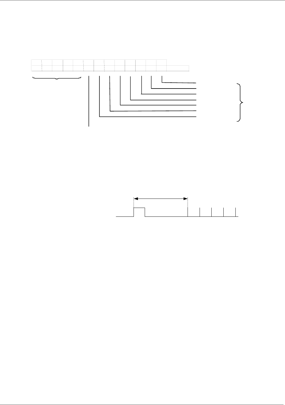
S6700 Multi-Protocol Transceiver IC - Reference Guide June ’02
4.1 General Remarks and Basic Command Structure
The protocol uses a simple three wire serial link between the Transceiver IC and a
remote controller (microprocessor) to transmit data and set up data. All signals trav-
elling on this interface must be resynchronised and debounced. It is important to al-
low a 70 ns debounce time before looking for any signal change. For example, if
SCLOCK rises 70 ns before DIN the Transceiver IC serial interface may see them as
rising together.
For each communication, the remote controller must send a command to perform an
appropriate sequence. A typical command is structured as follows: (S1, eight bits
command, data, ES1). More actions may follow a specific command but sending S1
will in general initiate a new sequence.
A sequence is defined as being all signals between the first S1 (that belongs to the
sequence) and the next S1 (that belongs to the next sequence).
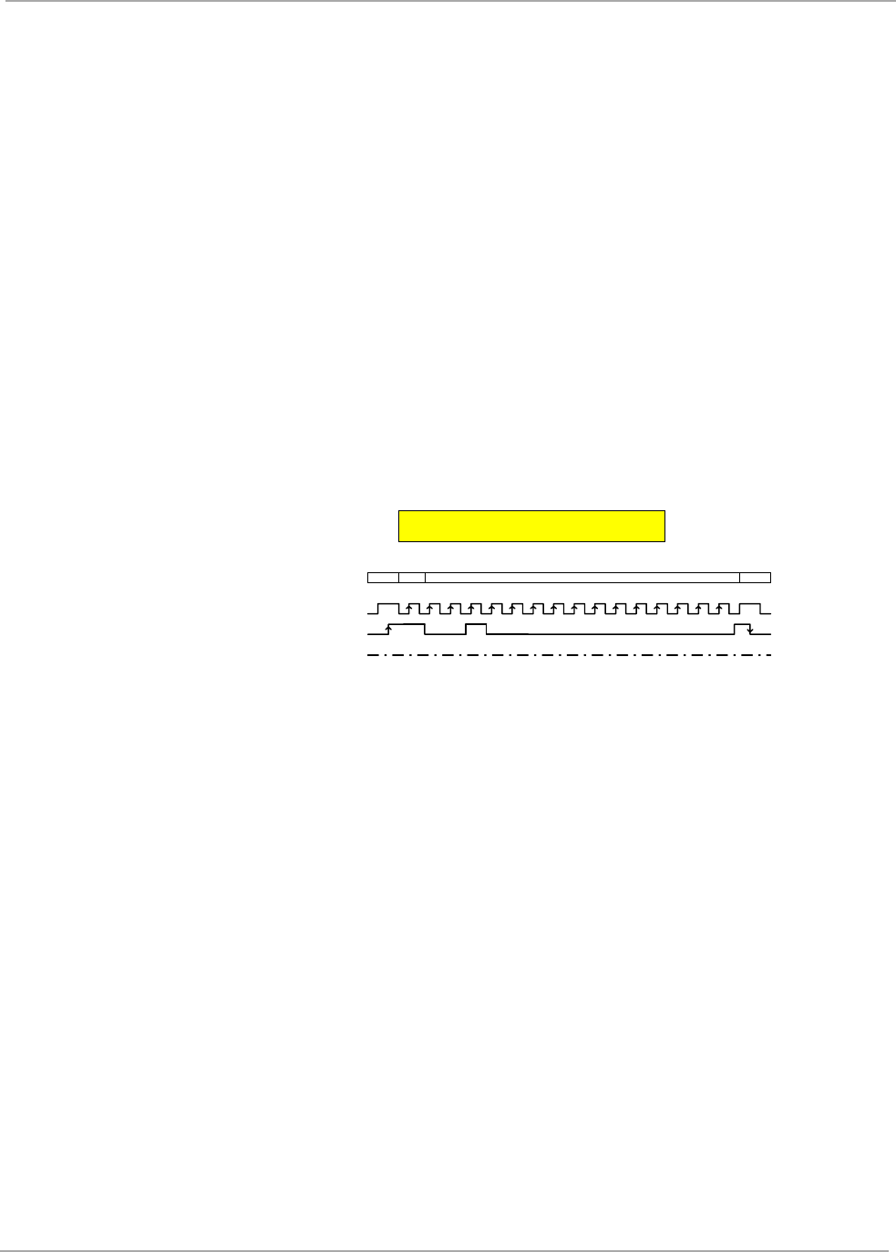
Figure 8: Command Structure
4.1.1 Definition of Start (S1), Stop (ES1) and Data bit
Start, stop, and data are indicated by the sequences:
- Start (S1) is defined as the start of the communication sequence between the
Transceiver IC and the micro-controller. It is a low-to-high transition on the DIN
line while SCLOCK is held high.
- Stop (ES1) is defined as the end of the communication sequence and is a
high-to-low transition on the DIN line while SCLOCK is held high.
- Each data bit is latched by the rising edge of SCLOCK. The value of the data
bit must be settled and has to remain the same while SCLOCK is high.
- The data on DIN can be changed while SCLOCK is low.
Size/length
S1 Start 1 Bit
Command Command byte 8 Bits
Bin. Data Binary data X Bits depending on message
ES1 Stop 1 Bit
Note:
You should switch the transmitter on (as described in section 4.1.4)
before you send the first command, otherwise it could happen that the
first command is not correctly performed.
S1 ES1B-DataCMD
bit 7 bit 0
Start Command Stop
Bin. Data
21
June ’02 Chapter 4. Protocol Definition
Figure 9: Definitions
4.1.2 Command byte definition
The command byte is defined in Table 5.
The configuration commands are used to communicate with the Transceiver IC ac-
cording to Table 7 below.
Table 5: Command Byte Definition
Bit no Description Function in High Level Function in Low Level
7 Mode bit 1 = Register Mode 0 = Normal Mode
6Table 6
Mode is selected according to Table 6
ISO 15693 (1out of 4) is the default register setting
5Table 6
4Table 6
3Modulation
Depth 1 = 100% 0 = 10%
2 AM / FSK 1 = AM selected 0 = FSK selected
1 Baud rate 1 = High Baud rate
According to ISO 15693
0 = Low Baud rate
according to ISO 15693
0 Parity of first byte Even parity
Table 6: Meaning of Bits 4, 5 & 6
Bit # 6 Bit # 5 Bit # 4 Definition
000 Direct Mode
0 0 1 Tag-it protocol
0 1 0 ISO 15693 / down link 1 out of 4
0 1 1 ISO 15693 / down link 1 out of 256
1 0 0 ISO 14443 Mode A
101 Reserved
110 Reserved
1 1 1 Configuration commands Table 7
Sclock
Din
Definitions
Symbolic S1= Start ES1 = StopBit = 1 Bit = 0
T1 T2 T3 T4 T5 T6
Minimum timings
T1: 300 ns T4: 600 ns
T2: 300 ns T5: 300 ns
T3: 66 ns T6: 300 ns
22
S6700 Multi-Protocol Transceiver IC - Reference Guide June ’02
4.1.3 Transmitter Off Command
Figure 10 shows a special and fast command to shut down the carrier. This can be
constructed with an S1 sequence followed by an ES1 sequence. Therefore, this has
been written 'S1' and 'ES1' in the symbolic representation.
The transmitter is kept 'ON' after a RF command was initiated. To switch the trans-
mitter OFF the following sequence is used:
- A transition of SCLOCK from low -to-high.
- A low -to-high transition followed by a high-to-low transition on the Din line
while SCLOCK is held high the whole time.
- A transition of SCLOCK from high to low.
Figure 10: Shut Down Command
The width of the pulse of Din must be at least 1.2 µs in order to secure the system,
and avoid any confusion between a TXOFF command and an S1 command, in case
any spurious spike(s) are present on the serial link.
It is not necessary to switch off the transmitter before sending another command and
data stream to the Transceiver IC.
4.1.4 Transmitter On command
The transmitter can be switched on with each of the RF commands in Table 5 except
for the configuration commands. The fastest command to switch the transmitter on
is a register mode command without data, using the sequence: S1, 1, ES1.
Table 7: Configuration Commands
Bit # 7 Bit # 6 Bit # 5 Bit # 4 Bit # 3 Bit # 2 Bit # 1 Bit # 0 Definition
01110001Read from Configuration Register
01111101Write to Configuration Register
01111110Power down
Note:
An overview of supported Command Bytes is given in Appendix B.
Symbolic
Sclock
Din
Dout
TX OFF
'ES1''S1'

23
June ’02 Chapter 4. Protocol Definition
4.2 Operating Modes
There are two operating modes available: normal mode and register mode.
4.2.1 Common Points (Normal and Register Mode)
Following the S1 bit and the command (either normal or register mode), the rest of
the sequence is the same.
The number of data bits is arbitrary. The controller sends ES1 when all data bits have
been sent. It is the responsibility of the controller to check that the number of data
bits is consistent. For example, sending 7 data bits in mode 1out 256 is not consist-
ent. The controller will have no feedback on this error, wrong data or no data at all
could be sent. The various CRC sent by the TAG should allow the controller to un-
derstand its mistake and, if necessary, to reinitiate a sequence.
The first bit ES1 will probably not finish the sequence since an answer from the TAG
will probably be expected. This is explained in figures 12, 14 and 15.
Note that S1 starts the sequence but does not physically modulate the carrier with a
SOF. The SOF will be generated by the Transceiver IC itself before sending data.
This SOF may depend on the mode. It may only be sent after several data bits have
been received by the Transceiver IC. For example, the SOF may be modulated only
when 8 bits have been received in the mode 1 out 256. This behaviour is similar in
the mode 1 out of 4.
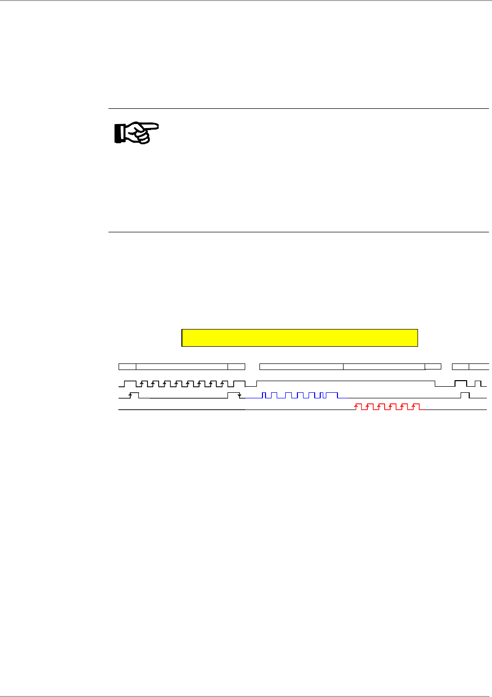
4.2.2 Normal Mode
Figure 11 represents the “Normal Mode”. The user sends some configuration inside
the command (definition see Table 5) and starts sending data that will be transmitted
by the way of modulating the carrier. SOF, data, EOF will be sent to the TAG. There
is no timing correlation between the data in the serial interface and the timing of the
data transmitted to the TAG. This is the reason why a buffer (FIFO) has been imple-
mented in the Transceiver IC. The signals related to the FIFO will be described in
FIFO management section 4.5.2.
Figure 11: Normal Mode
Example:
The data stream to address the Tag-it RF protocol is defined by the following se-
quence:
Size/length
Start (S1) 1 Bit
Command byte Bit #7 = L, Normal Mode
Bit #6 = L, Tag-it protocol
Bit #5 = L, “
ES1
data= to be sent to TAG
Normal Mode
Symbolic
Sclock
Din
Dout
command= normal mode
b7
S1
FIFO management is not shown here
b0
24
S6700 Multi-Protocol Transceiver IC - Reference Guide June ’02
Bit #4 = H, “
Bit #3 = H, 100% modulation
Bit #2 = L, FM demodulator
Bit #1 = H, this field is not applicable, it is set to default
Bit #0 = H, even parity
Data to the tag: Binary data are converted into the Tag-it RF-protocol
Stop (ES1) 1 Bit
4.2.3 Register Mode
Figure 12 represents the “Register Mode” command. This command is only one bit
long and not 8 bits long like all other commands.
In “Register Mode”, the configuration used is the one that has been previously pro-
grammed in the Transceiver IC. This configuration should be written using “Write to
Configuration Register” (Figure 14) during a previous communication with the Trans-
ceiver IC.
The Configuration Register definition is shown in Appendix C.
Figure 12: Register Mode
Example:
The data stream to address the RF protocol as defined in the registers is given by
the following sequence:
Size/length
Start (S1) 1 Bit
Command byte Bit #7 = if High the mode is set according to the
register settings.
Data to the tag: Arbitrary length binary data stream. The bits are en-
coded according to the protocol format defined in
the RF protocol registers
Stop (ES1): 1 Bit
ES1data= to be sent to TAG
Register mode
Symbolic
Sclock
Din
Dout
cmd
b7
S1
FIFO management is not shown here
25
June ’02 Chapter 4. Protocol Definition
4.3 RF Protocol
4.3.1 General
A description of the RF Protocol according to ISO 15693 and ISO 14443 can be
found in the relevant ISO documentation. The Tag-it protocol for Tag-it HF trans-
ponders is described in the Tag-it protocol, TI specification 11-04-21-002.
4.3.2 Direct Mode
In Direct Mode, the controller has to create all modulated signals sent to the TAG
since the transmitter input is directly connected to the input line Din. This signal has
the exact timing required by the TAG.
Figure 13: Direct Mode
The 'Direct Mode' is entered by S1, command (8 bits), ES1 and the Transceiver IC
is then set to “direct Mode”. At this point, no carrier modulation has been applied to
the TAG. After SCLOCK rises, DIN can directly control the modulation input, which
is then directly connected to the RF modulator.
The modulation depth 10% or 100%, the receiver channel settings and the demodu-
lation mode AM/FSK are defined by the command byte. The raw demodulated data
(Manchester coded) is available at DOUT and no further processing is performed by
the Transceiver IC when operating in this mode.
To exit this mode the SCLOCK line changes from high-to-low and the transmitter is
switched off.
Notes:
The transmission direction of the binary data depends on the defini-
tion of the selected RF Protocol and can be different between the
command byte and the binary data (RF Protocol). For example: for
ISO 15693 and ISO 14443 you must send the LSB first.
The binary data response for the Tag-it protocol and the ISO 15693
protocol contains two additional zeros (0 0) in the end of frame, to
indicate the end of transponder transmission. This sequence is
decoded as “0 0 ES”. The two zeros must be removed from the data
string before any further processing.
Symbolic
Sclock
Din
Dout
cmd=direct modeS1 Data = to be sent to TAGES1 TAG data manchester coded S1 new cmd
Direct Mode
TX off
26
S6700 Multi-Protocol Transceiver IC - Reference Guide June ’02
4.4 Register Configuration
4.4.1 Write Data to Configuration Register
The data bits following the command byte are written to the configuration register.
Figure 14: Write Configuration Register
Figure 14 represents the command “Write to Configuration Register” since the 8 bits
of command are 01111101. The data stream illustrated in Figure 14 is 8 bits long.
This sequence is used to define the active settings when operating in “Register
mode” (see sequence “'Register Mode”). The values for Bit 7 “Idle Mode” and bit 0
“Manchester Decoder” are also valid for “Normal Mode”.
After the bit ES1, the command “Write to Configuration Register” is finished. A new
bit S1 is expected to initiate a new sequence.
4.4.2 Read Data from Configuration Register
Read Data from Configuration Register: The data after the command byte are the
content of the registers and clocked out by the SCLOCK from the controller.
Figure 15: Read from Configuration Register
Figure 15 shows the “Read from Configuration Register” command, which is
01110001. The controller is reading the configuration register of the Transceiver IC.
This has nothing to do with the presence of a TAG or not. The controller can consider
this operation as reading a RAM via the three wires serial link interface. The control-
ler is allowed to send ES1 before having read all configuration bits if it does not need
to know all bits. The order of the configuration bits inside the Transceiver IC is then
important in case a specific part of the configuration is read frequently.
After the bit ES1, the command “Read from Configuration Register” is finished. A
new bit S1 is expected to initiate a new sequence.
ES1data= Configuration data to write
Write to Configuration Register
Symbolic
Sclock
Din
Dout
command=Write to Configuration Register
b7 b0
S1
ES1data = Configuration Register data on DoutSymbolic
Sclock
Din
Dout
command = Read from Configuration Register
b7 b0
S1
ESdata = Configuration dataSymbolic
Sclock
Din
Dout
command = Read from Configuration Register
b7 b0
S1
Read from
Configuration
Register
interupted
by RC
Read from Configuration Register
27
June ’02 Chapter 4. Protocol Definition
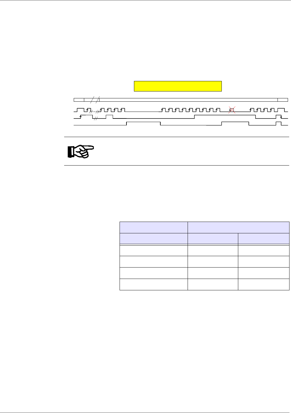
4.5 Communication
4.5.1 FIFO Management
Because the micro controller cannot control the timing of sending data to the TAG
the Transceiver IC must store the data from the micro controller. The capacity of stor-
age being limited, management of the buffer must be implemented. The buffer is im-
plemented as a 16 bit FIFO.
Figure 16: FIFO Management
The FIFO management is shown in Figure 16. The Transceiver IC indicates that its
buffer is full and asks the controller to stop sending data. The Transceiver IC does
so by raising DOUT while SCLOCK=0. The controller must wait until DOUT returns
to level 0 to send further data. The Transceiver IC indicates that its buffer is almost
empty under the following conditions:
Data is written with the commands “Write ASIC”, “Normal Mode” and “Register
Mode”. The FIFO management is not needed for the “Write ASIC” command, since
writing in the Transceiver IC is immediate. FIFO management will be used with the
“Normal Mode” and “Register Mode” commands.
Note:
As long as DOUT is at level 1 it is not permitted to send a clock signal
on the SCLOCK line.
Table 8: Overview of #Bits present in FIFO
# Bits present in FIFO
Mode DOUT is rising DOUT is falling
Tag-it 16 3
ISO 15693 1 out of 4 16 2
ISO 15693 1 out of 256 16 7
ISO 14443 16 3
data= to be sent to TAGSymbolic
Sclock
Din
Dout
cmdS1 ES1
FIFO Management
28
S6700 Multi-Protocol Transceiver IC - Reference Guide June ’02
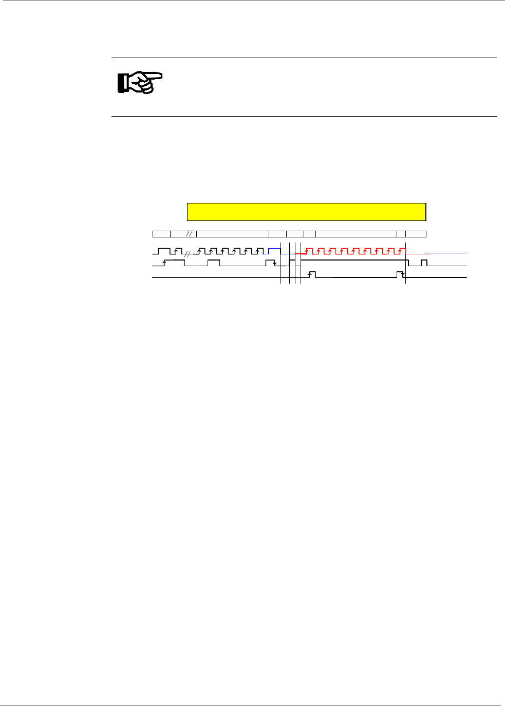
4.5.2 Basic Request/Response
The SCLOCK line becomes bi-directional.
DIN is always input for the Transceiver IC
DOUT is always an output for the Transceiver IC
SCLOCK is used by the Transceiver IC and the controller
Figure 17: Basic Request/Response
S1, cmd//, and ES1 are sent (cmd// = “normal mode” OR “register mode”). A SOF
followed by the data and terminated by EOF is transmitted to the TAG by amplitude
modulation of the carrier. (Remark: the FIFO management is not shown in figures 13,
15 and 17).
In a typical case, the TAG will now send its answer to the request. The ASIC has to
control the line SCLOCK since the data rate of the TAG will pace the data flow.
4.5.2.1 Definition TRAN1
During Transient 1 (TRAN1), the controller gives control of the SCLOCK line to the
Transceiver IC: DIN =0
Time a: The bit ES1 is finished.
Time b: The controller raises DIN, either to prepare a control mode change for
the SCLOCK line or to prepare an ES1.
Time c: DIN is falling. The controller definitely indicates that it will give the
SCLOCK line control to the Transceiver IC. SCLOCK =0 and both the
controller and the Transceiver IC are outputs.
Time d: DIN rises showing that the controller leaves the control of the bus until
DIN falls to ask the control of SCLOCK back. At time d, SCLOCK is still
equal to 0 but the pin SCLOCK of the controller is an input and the pin
SCLOCK of the Transceiver IC is an output.
When the Transceiver IC has control of SCLOCK, it will send a S2 that corresponds
to a SOF sent by the TAG, the data (7 bits in Figure 17) and an ES2 that corresponds
to the EOF of the TAG.
4.5.2.2 Definition TRAN2:
During Transient 2, the controller regains control of SCLOCK: DIN =1
The controller indicates its intention to regain control over SCLOCK by setting DIN=0
and initiate a change by making a pulse on DIN. It is during this pulse that the line
SCLOCK will change direction.
Note:
For the sake of clarity we have introduced a new convention: When
the Transceiver IC drives the line SCLOCK the start of the sequence
is marked S2 and the end ES2.
data= to be sent to TAG
Basic Request / Response
Symbolic
Sclock
Din
Dout
cmdS1 ES1
abcd e
TRAN1 S2 TAG data ES2 TRAN2

29
June ’02 Chapter 4. Protocol Definition
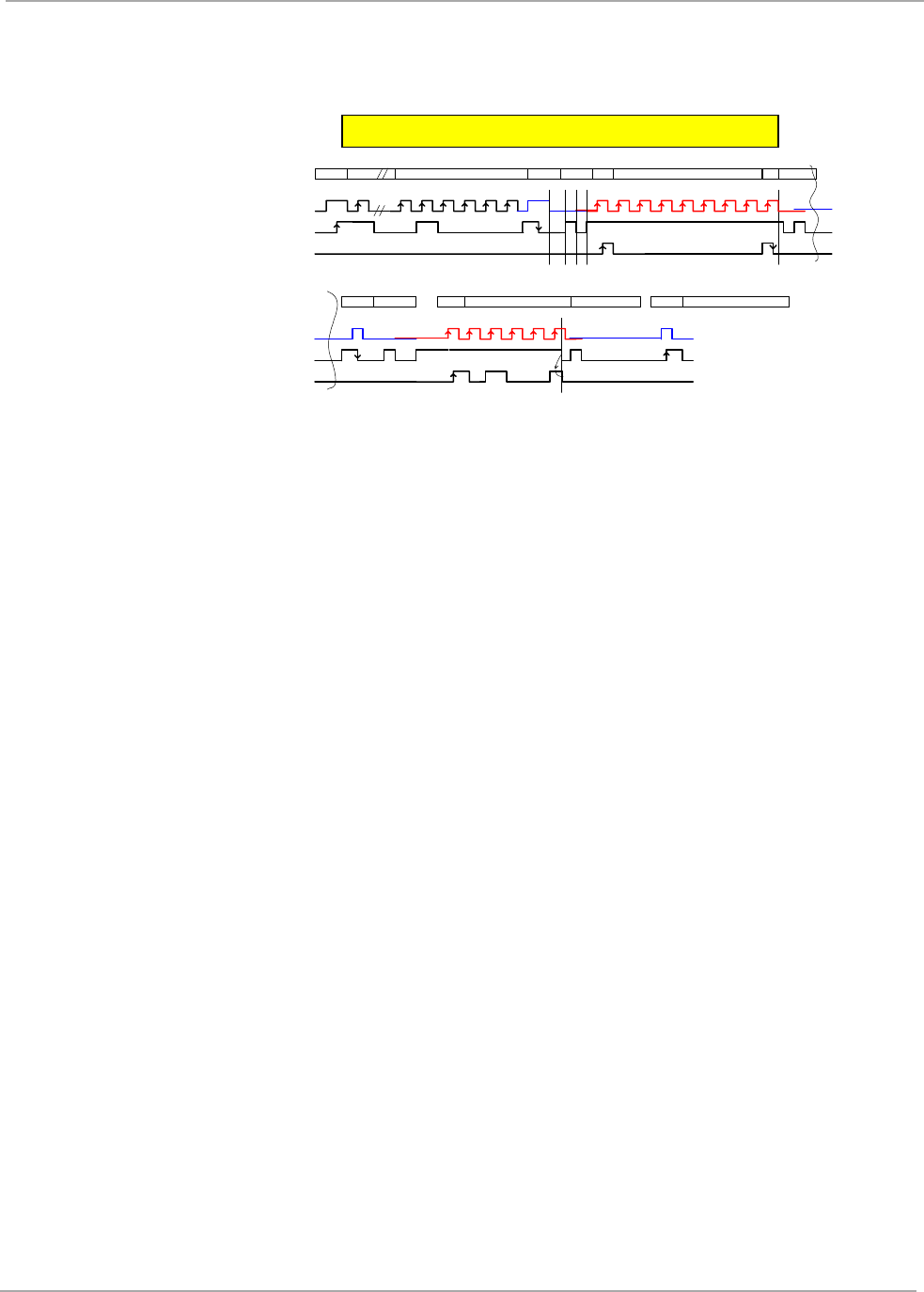
4.5.3 Bi-directional SCLOCK
Figure 18 shows an extreme case of successive changes of SCLOCK control. This
example demonstrates the principle, its purpose is not to show a typical case. Even
if this could be done, it is very unlikely that a user would implement such a case.
Figure 18: Bi-directional SCLOCK
A classical TRAN1 is shown at times a, b and c of Figure 18. This is described in sec-
tion 4.5.2.1.
At time d, the controller signals that it wants to take back control of SCLOCK. DIN
rises at time e. Between time e and time f, SCLOCK=0 both Transceiver IC and con-
troller are outputs. At time f, only the controller is an output.
At time g, the controller raises DIN to prepare an ES1.
Between time h1 to h2, a classical TRAN1 is performed. At time h2, the Transceiver
IC controls SCLOCK.
At time i, the Transceiver IC raises DOUT to be ready to send a data '1' to the con-
troller as SCLOCK is rising. At the same time (before or after), the controller resets
DIN showing it wants to take back the bus.
The falling of DOUT while SCLOCK=1 is normally an ES2.
At time k, the Transceiver IC resets SCLOCK to low. After this a TRAN2 can take
place. At time l, both Transceiver IC and controller are outputs. At time m, the Trans-
ceiver IC is an input and the controller is an output.
Symboli
c
Sclock
Din
Dout
Bi-directional SCLOCK
TRAN2TRAN1 ES1 TRAN1 data TRAN2
abc def g h2 ijklm
h1
30
S6700 Multi-Protocol Transceiver IC - Reference Guide June ’02
4.5.4 Simultaneous Identification (SID) / Anti-collision
Figure 19: Simultaneous Identification (SID) / Anti-collision
When you have read section 4.5.3 you (controller software developer) have all the
elements to establish a SID with the TAG, this is shown in Figure 19.
The sequence S1, cmd//, data, ES1, will send to the TAG a SOF, Data (=SID re-
quest), EOF. The last EOF can normally be seen as the marker of the beginning of
the first slot. The first TRAN1 allows the Transceiver IC to send the data received
from the TAG. The first bit sent is S2 (corresponding to a SOF sent by the TAG), TAG
data (7 bits on Figure 19), ES2 (corresponding to the EOF sent by the TAG). A
TRAN2 gives back the SCLOCK to the controller.
ES1 is then sent to modulate an EOF towards the TAG, delimiting a new slot. The
next signals are TRAN1, S2, TAG data (only 4 bits) but at this time, the controller is
not interested in continuing to read data. At time f, the controller resets DIN to ask for
control of SCLOCK. The Transceiver IC stops the process TRAN2 since
SCLOCK='1' by resetting DOUT. As soon as SCLOCK='0', the Transceiver IC ac-
knowledges it is ready to begin a TRAN2 by raising DOUT='1'. A TRAN2 can now
take place to give back the control to the controller.
Finally, the controller decides to start a new sequence by sending S1, which com-
pletes the SID sequence.
The two slots shown, as an example, are not typical since 16 slots may be used in
normal operation.
data= to be sent to TAG
Simultaneous Identification (SID)
Symbolic
Sclock
Din
Dout
cmdS1 ES1
abcd e
TRAN1 S2
f
TAG data ES2 TRAN2
ES1 TRAN1 S2 TAG data TRAN2 S1 new commandSymbolic
Sclock
Din
Dout
see below

31
June ’02 Chapter 4. Protocol Definition
4.6 Power Management
4.6.1 Idle Mode
The Transceiver IC can be switched to Idle mode by configuring Bit 7 of the Config-
uration Register to 1 with the command “Write to Configuration Register”. In this
mode, only the oscillator and the essential digital circuits are enabled. It can be
switched out of Idle mode by configuring Bit 7 of the Configuration Register to 0.
4.6.2 Power Down Mode
The Transceiver IC can be switched into “Power Down Mode” by sending the Power
Down configuration command (01111110) as described in section 4.1.2 and Table
7.
In Power Down Mode, the crystal will not be running, some analog circuitry may be
shut down, the carrier will be off, the configuration bits remain unchanged.
Consequently, the serial link (clocked by the crystal) will not be available. The con-
troller cannot communicate with the Transceiver IC in this mode.
To wake the Transceiver IC up, the controller has to send a bit S1 that will trigger
some asynchronous circuitry on board of the Transceiver IC. This action will reset
(asynchronously) the bit 'Power Down', and will restart the crystal oscillator. After a
delay of 10 ms, the serial link will operate again.
During a wake up phase, the controller will have to wait until the crystal oscillator has
reached its nominal operating conditions again. The controller (after this delay)
should initiate a new sequence (S1, cmd, and data, ES1). Note that the bit S1 used
to wake up the Transceiver IC is not initiating a sequence. In practice, to write a new
sequence to the Transceiver IC when the Transceiver IC is in Power Down Mode,
the controller must do: S1, delay (10 ms), S1, cmd, data, ES1 (where cmd can be
any command).
4.7 Pin M_ERR
The pin M_ERR is an output and has three functions:
- It will rise during ES1 if the bit #0 (parity) is wrong in the command
- It will rise as soon as bad data is decoded by the Manchester decoder while
receiving data. This tells the controller that the common bits of two Tags an-
swered at the same time within the same slot or the timing offset for synchro-
nizing of the Manchester decoder needs to be adjusted (see Appendix C -
Timing Register).
- If the FIFO Buffer is empty and the reader to transponder communication is
finished then a 22 µs pulse is generated on the M_ERR pin.

CHAPTER 5
32
Regulatory, Safety and Warranty Notices
Chapter 5:Regulatory, Safety and Warranty Notices
This chapter provides important information about regulatory constraints and safety
precautions.
Topic Page
5.1 Regulatory Notes .....................................................................................33

33
June ’02 Chapter 5. Regulatory, Safety and Warranty Notices
5.1 Regulatory Notes
An RFID system comprises an RF transmission device, and is therefore subject to
national and international regulations.
Prior to operating the S6700 Transceiver IC as a system together with antenna(s)
and power supply, the required FCC, PTT or relevant government agency approval
must be obtained. Sale, lease or operation in some countries may be subject to prior
approval by the government or other organization.
APPENDIX A
34
Application Examples
Appendix A:Application Examples
An Application Schematic which has been optimized to drive a 50 Ω resistive anten-
na using a 5 V power supply is shown in Figure 20.
Figure 20: Application Circuit
Table 9: Parts List for Application Circuit
Component Value Component Value
C1 10nF L1 4.2µH
C2 56pF L2 5.6µH
C3 10µF Tantalum L3 1.2µH
C4 100nF - -
C5 22pF R1 2.2kΩ
C6 100nF R2 12Ω
C7 22pF - -
C8 100nF - -
C9 47pF - -
L2
µC
A
NTENNA
C4C3
C7
1
2
3
4
5
6
7
8
9
10 11
12
13
14
15
16
17
18
19
20
VDD_TX
TX_OUT
R_MOD
VSS_TX
XTAL1
XTAL2
VSS_DIG
XTAL_CLK
DOUT
VDD_DIG
DIN
M_ERR
SCLOCK
VDD_RX
VSS_RX
RX_IN
VCC
VCC
C2
R1
XTAL 13.56 MHz
VCC
L3
C8
C6
L1
COAX
C5
R2
C9
C1
35
June ’02 Appendix A. Application Examples
At 5 V, this circuit will output typically 200 mW RF power when a suitable matched
50 Ω antenna is connected. At 3 V the output will be typically 80 mW RF power. Pro-
portionately lower RF outputs will result if you only have a simple resonating circuit.
Where the transmitter is intended to be on all the time, it is recommended that the
chip pad sizes and tracks are increased to provide a larger area for heat dissipation.
Care should be taken with board design to avoid excessive capacitance. When board
capacitance is too high, the value of the capacitance associated with the crystal may
need reducing to avoid an unstable clock. The suggested circuit shows capacitor val-
ues of 22 pF.
The Transceiver IC can be switched from 100% to 10% via the software. ISO 15693
specifies that the inlay should perform with modulation depths between 10% and
30% (in addition to 100%) and the required depth can be configured by changing re-
sistor R2 in the suggested circuit. Table 10 shows the resistance values required in
to change the depth of modulation.
Table 10: Modulation Resistor Values
Modulation%
Resistor
Value
(Ω
ΩΩ
Ω)
Comment
10 12 Minimum modulation depth
20 18 Recommended modulation depth
30 25 Maximum modulation depth
Note:
In order to achieve the highest possible read-out coverage we recom-
mend that you operate the reader at a modulation depth of 20% or
higher.

APPENDIX B
36
Command Byte Overview
Appendix B:Command Byte Overview
An overview of the Transceiver IC’s Command Byte is shown on the next page.

37
June ’02 Appendix B. Command Byte Overview
Operation Mode 0=Normal Mode
RF Protocol
Modulation 0=10% , 1=100%
Subcarrier 0=FM (two subcarrier) , 1=AM (one subcarrier)
Data Rate 0=Low Data Rate , 1=High Data Rate
Parity set Parity to have EXOR(bit7..0)=0
RF Protocol Modulation Subcarrier Data Rate
00000000 not applicable
0 0 0 0 0 0 1 1 Direct Mode 10% FM ----
0 0 0 0 0 1 0 1 Direct Mode 10% AM ----
00000110 not applicable
00001001 not applicable
0 0 0 0 1 0 1 0 Direct Mode 100% FM ----
0 0 0 0 1 1 0 0 Direct Mode 100% AM ----
00001111 not applicable
00010001 not applicable
00010010 not applicable
00010100 not applicable
00010111 not applicable
00011000 not applicable
0 0 0 1 1 0 1 1 Tag-it Protocol 100% FM High Data Rate (26.69kbit/s)
00011101 not applicable
00011110 not applicable
0 0 1 0 0 0 0 1 ISO 15693 (1 out of 4) 10% FM Low Data Rate (6.67kbits/s)
0 0 1 0 0 0 1 0 ISO 15693 (1 out of 4) 10% FM High Data Rate (26.69 kbits/s)
0 0 1 0 0 1 0 0 ISO 15693 (1 out of 4) 10% AM Low Data Rate (6.62 kbits/s)
0 0 1 0 0 1 1 1 ISO 15693 (1 out of 4) 10% AM High Data Rate (26.69 kbits/s)
0 0 1 0 1 0 0 0 ISO 15693 (1 out of 4) 100% FM Low Data Rate (6.67kbits/s)
0 0 1 0 1 0 1 1 ISO 15693 (1 out of 4) 100% FM High Data Rate (26.69 kbits/s)
0 0 1 0 1 1 0 1 ISO 15693 (1 out of 4) 100% AM Low Data Rate (6.62 kbits/s)
0 0 1 0 1 1 1 0 ISO 15693 (1 out of 4) 100% AM High Data Rate (26.69 kbits/s)
0 0 1 1 0 0 0 0 ISO 15693 (1 out of 256) 10% FM Low Data Rate (6.67kbits/s)
0 0 1 1 0 0 1 1 ISO 15693 (1 out of 256) 10% FM High Data Rate (26.69 kbits/s)
0 0 1 1 0 1 0 1 ISO 15693 (1 out of 256) 10% AM Low Data Rate (6.62 kbits/s)
0 0 1 1 0 1 1 0 ISO 15693 (1 out of 256) 10% AM High Data Rate (26.69 kbits/s)
0 0 1 1 1 0 0 1 ISO 15693 (1 out of 256) 100% FM Low Data Rate (6.67kbits/s)
0 0 1 1 1 0 1 0 ISO 15693 (1 out of 256) 100% FM High Data Rate (26.69 kbits/s)
0 0 1 1 1 1 0 0 ISO 15693 (1 out of 256) 100% AM Low Data Rate (6.62 kbits/s)
0 0 1 1 1 1 1 1 ISO 15693 (1 out of 256) 100% AM High Data Rate (26.69 kbits/s)
01000001 not applicable
01000010 not applicable
01000100 not applicable
01000111 not applicable
01001000 not applicable
01001011 not applicable
01001101 not applicable
0 1 0 0 1 1 1 0 ISO 14443 (Type A) 100% AM High Data Rate (105.94 kbit/s)
0 1 1 1 0 0 0 1 Read from Configuration Register
01110010 not applicable
01110100 not applicable
01110111 not applicable
01111000 not applicable
01111011 Write to Timing Register
0 1 1 1 1 1 0 1 Write to Configuration Register
01111110 Power Down
Command Byte
APPENDIX C
38
Register Definition
Appendix C:Register Definition
Configuration Register
The Configuration Register has 8 bits which are defined as following:
Bit
7 Idle Mode Off=0 On=1
6
5 RF Protocol Definition
4
3 Modulation: 10%=0 100%=1
2 Two subcarrier (FM)= 0 One subcarrier (AM)=1
1 Data Rate: Low=0 High=1
0 Manchester decoder: enabled=0 disabled=1
The default (factory) configuration is: 00100010
Bit6
Bit5
Bit4
000Direct Mode
0 0 1 Tag-It Mode
0 1 0 ISO 15693 / down link 1 out of 4
0 1 1 ISO 15693 / down link 1 out of 256
1 0 0 ISO 14443 Mode A
101Reserved
110Reserved
111Reserved
39
June ’02 Appendix C. Register Definition
Timing Register
The timing register is used to set the sampling point of the digital decoder to generate
binary data from the Manchester coded data stream (Timing Offset). The time is de-
fined from the end of transmission from the Transceiver IC to the transponder until
the beginning of the response from the transponder.
Certain variations are allowed for this timing offset and depending on the signal
strength and signal-to-noise ratio seen at the receiver input a change of the default
value may result in better reading results.
For test purposes the boundary scan signals can be feed to the pin M-ERR by setting
bit D7.
Conditions to set the timing offset:
• The first rising edge of the boundary scan must be in front of the start of the tag
response.
• The first boundary scan pulse can be set by changing the Timing Offset Bits
D6..D0.
• The weight of one bit shifts Tdelay by 295 ns (4/13.56 MHz).
Changing the value of this register is done with the command '0111 1011' followed
by a 13-bit data stream.
Example: Set Tdelay to 311.31 µs
Send command '0111 1011' followed by the 13-bit data stream
'1100 0000 1001 0'.
D12D11D10D9D8D7D6D5D4D3D2D1D0
11 00 00 010 11 00 Default
Timing Offset1 LS B
Timing Offset2
Timing O ffset3 To adjust the
Timing Offset4 boundary scan
Timing Offset5
Timing Offset6
Timing Offset7 MS B
Boundary scan: 0 = Normal, 1 = Boundary scan is added on pin M_ERR
Reserved
need to be the
Default value
M_ERR
Tdelay

40
S6700 Multi-Protocol Transceiver IC - Reference Guide June ’02
The changed setting remains active until the device is disconnected from power.
data= Timing settings to writeSymbolic
Sclock
Din
Dout
command = Timing Setting
b7 b0
S1
ES1
Sclock
Din
Dout
cont.data= Timing settings to write

APPENDIX D
41
Terms & Abbreviations
Appendix D:Terms & Abbreviations
A list of the abbreviations and terms used in various TI-RFID manuals can now be
found in a separate manual:
TI-RFID Product Manuals - Terms & Abbreviations
Document number: 11-03-21-002

42
S6700 Multi-Protocol Transceiver IC - Reference Guide June ’02