Rising Digital SECD-3I5A-02 SECD-3I5A-02display screen User Manual Manual
Shanghai Rising Digital Co.,Ltd. SECD-3I5A-02display screen Manual
Manual

1st
Shanghai Rising Digital Co.,Ltd.
SECD-3I5A-02 USER MANUAL
Document Number:
Dense level:
Version Number: V1.2

2nd
Shanghai Rising Digital Company
Revision History
Version Date AMD Reviser Instructions Approval
1.0 2012-09 A
Hongliang Liu,
Xiang Gao
Creation
(A-Add,M-Modify,D-Delete)
3r
d
SECD-3I5A-02(4GVersion)
1、Hardware performance indicators
1) Voltage input:
¾ circuits:4
¾ signal:0~5V.DC
¾ precision:0.5%
¾ resolution:0.025%
2) Resistance input :
¾ circuits:2
¾ precision:0.5%
¾ resolution:0.025%
3) Discrete input(low level):
¾ circuits:5
¾ signal peak:0~40V.DC
¾ frequency:0Hz~1KHz
4) Discrete input(high level):
¾ circuits:2
¾ signal peak:0~40V.DC
¾ frequency:0Hz~1KHz
5) Periodic input:
¾ circuits:1
¾ signal peak:1.2~40V.DC
¾ range:10Hz~70KHz
¾ precision:0.1%
6) PWM output:
¾ circuits:1
¾ frequency:50~2.55kHz
¾ current:0~0.75A
¾ precision:1%
¾ resolution:0.025%
4th
¾ features:overpressure、short circuit protection
7) Motor driver output:
¾ circuits:4(one stepper motor)
¾ contact capacity:40V.DC 1.2A
¾ frequency:0Hz~3KHz
¾ features:overpressure、short circuit protection
8) Digital output:
¾ circuits:4
¾ contact capacity:40V.DC 1.8A
¾ frequency:0Hz~1KHz
¾ features:overpressure、short circuit protection
9) Analog output:
¾ circuits:1
¾ signal peak:0~5V.DC
¾ precision:0.5%
¾ resolution:0.025%
10) Communication interface:
¾ CAN:1circuit,Rate of optional,ISO11898 CAN 2.0B、J1939
¾ Communications link:1circuit,4G/GSM
North American version- frequency band LTE-FDD B2/4/5/12/17,
WCDMA B2/4/5,GSM 850/1900
The European version—frequency band LTE-FDD B1/3/5/7/8/20,
WCDMA B1/5/8,GSM 850/900/1800/1900
The Chinese version—frequency band LTE-FDD B1/3/8,LTE-TDD
B38/39/40/41, WCDMA B1,TD-SCDMA B34/39, GSM
900/1800
¾ GPS link:1 circuit
11) Display parameters:
¾ resolution:320×240(3RGB)
12) Other indicators
¾ kernel: TMS320F28335(32bit DSP)
¾ proposed kernel:112.5MHz
¾ duty cycle: ≤5 ms
5th
¾ power supply: 18~36V.DC(Under the recommended
voltage 24 v DC 36 v can't work for a long time)
¾ output voltage: 5V.DC,0.75A
¾ Current consumption: 0.2A.DC(24V.DC)
¾ Working temperature: -20~+65℃
¾ Storage temperature: -25~+80℃
¾ overvoltage protection: 37.2V
¾ high temperature protection:80℃
¾ protection grade: IP65,all-round protection
¾ relative humidity: 10%~90%
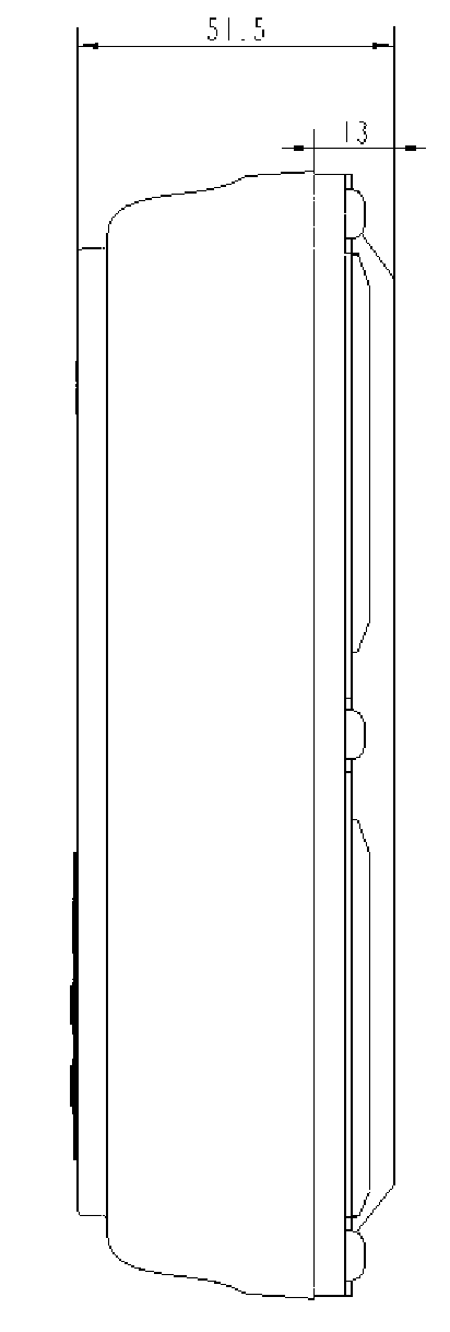
¾ overall dimensions: 183mm×127mm×51.5mm

6th
2、Installation drawing
Front view

7th
Rear view
8th
Right side chart

9th
Figure of the side

10th
3、Pin definition

11th
4、Terminal blocks that:
Signal name Parameter I/O
type Unit Range Precision Terminal number Instructions
Positive +24VIN Analog
input V 18~36 J1-25, J1-34 Analog output without load (open), switch
output without load (open), PWM output without
load (open), the standard + 24 VDC power
supply, the current consumption of about 0.2 A.
Negative GND Analog
input V 0 J1-8,J1-24,J1-33
Voltage input AI_V_i
(i=4)
Analog
input V 0~5 0.5% J1-21,J1-29,J1-30, J1-32
Resistance
input
AI_R_i
(i=2)
Analog
input Ω 0~130 0.5% J1-23,J1-31
A/D
AI
GND
+5VOUT
A/D
AI
GN
D
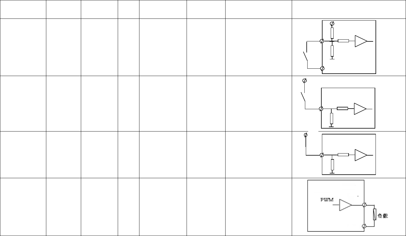
12th
Signal name Parameter I/O
type Unit Range Precision Terminal number Instructions
Discrete input
(low level)
DI_L_i
(i=1~5) Digital input V 0~40 J1-6,J1-12,J1-13,
J1-14,J1-15
Discrete input
(high level)
DI_H_i
(i=2) Digital input V 0~40 J1-4,J1-5
Periodic input TI_i
(i=1) Digital input Hz 10~70000 0.1% J1-3
Analog
output
A0_i
(i=1)
Analog
output V 0~5 J1-22
I/O
GND
DI
PI
I/O
PI
+24V
I/O
+24V
DI
13th
Signal name Parameter I/O
type Unit Range Precision Terminal number Instructions
PWM output PWM_i
(i=1)
Analog
output A 0~1.5 1% J1-10
CAN
high level line CAN_H Digital
input
output
V 2.5~5
0~2.5
J1-2
CAN by way of bus connection,terminal
120Ω resistance
CAN
low level line CAN_L J1-1
Program
reshipment jump
line
RS Digital
input J1-7 RS short, after receiving the program can
be heavy on electricity.
+5V power
output +5VOUT Analog
output V 5.0 ±5% J1-9 The external device, such as sensor with
power supply
Sleep mode
input SMI Digital
input V 0~36 J1-17
1) 0<SMI<6.5V
The controller into sleep mode;
2) 11V<SMI<36V)
Controller into the normal working mode.
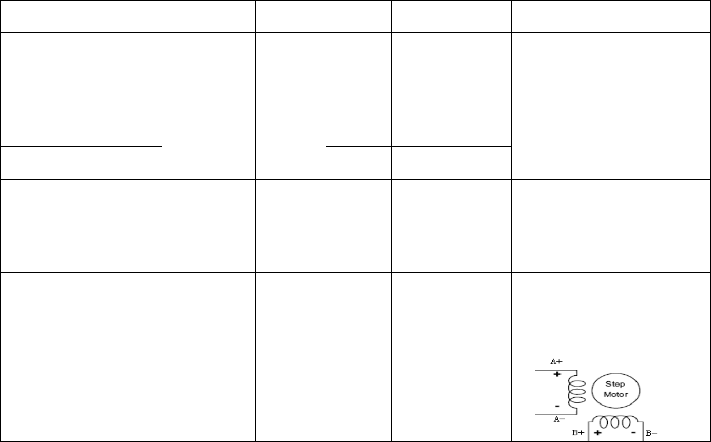
Motor driver output MO_i
(i=4)
Digital
output V 0~36 J1-11,J1-16 J1-19,J1-20

14th
5、Matters needing attention:
¾ 1、besides display shell well grounded, all connected to display the load, and so on input and output points must connect into a
closed loop, which all of the input and output must be connected with display corresponding to.
¾ 2、4G, GPS antenna installation, pay attention to the antenna will tighten the joint after use.
6、Radiation Exposure Statement
This transmitter must not be co‐located or operating in conjunction with any other antenna or transmitter. This device must be
installed and operated with a minimum distance of 20 cm away from radiator/antenna to user body.
7、Declaration of Conformity
Hereby Shanghai Rising Digital Co.,Ltd., declares that this SECD-3I5A-02display screen, SECD-5I7C-02 display
15th
screen,SECD-710F-02 display screen (Model No. SECD-3I5A-02, SECD-5I7C-02, SECD-710F-02) is in compliance with the
essential requirements and other relevant provisions of Directive 1999/5/EC.
Input Power:7~37 DC V, Normal 24DC V
Rating Current: 0.2A
Ambient Temperature ranges -20~+65℃℃
This device must be installed and operated with a minimum distance of 20 cm between the radiator and user body.
Manufacture
Shanghai Rising Digital Co.,Ltd.
Address:
No 318 ,Chuanda Road , Pudong New District, Shanghai,China
8、FCC Statement
FCC identification number is not visible when the device is installed inside another device, then the outside of the device into which
16th
the device is installed must also display a label referring to the enclosed device. This exterior label can use wording such as the
following: “FCC ID: 2AJONSECD-3I5A-02”
This device complies with part 15 of the FCC Rules. Operation is subject to the following two conditions:
(1) This device may not cause harmful interference, and
(2) This device must accept any interference received, including interference that may cause undesired operation.
Changes or modifications not expressly approved by the party responsible for compliance could void the user's authority to operate
the equipment.
NOTE: This equipment has been tested and found to comply with the limits for a Class B digital device, pursuant to Part 15 of the
FCC Rules. These limits are designed to provide reasonable protection against harmful interference in a residential installation. This
equipment generates, uses and can radiate radio frequency energy and, if not installed and used in accordance with the instructions,
may cause harmful interference to radio communications. However, there is no guarantee that interference will not occur in a
particular installation. If this equipment does cause harmful interference to radio or television reception, which can be determined by
turning the equipment off and on, the user is encouraged to try to correct the interference by one or more of the following measures:
‐‐ Reorient or relocate the receiving antenna.
‐‐ Increase the separation between the equipment and receiver.
‐‐ Connect the equipment into an outlet on a circuit different from that to which the receiver is connected.
‐‐ Consult the dealer or an experienced radio/TV technician for help.
The radios in this device have been designed and manufactured to not exceed stipulated emission limits for exposure to radio
frequency (RF) energy as required by the Federal Communications Commission of the U.S. Government 47 C.F.R. § 2.1091 and
17th
2.1093.
The antennas should be put up by the professional parts who take full responsibility for compliance with FCC15.203