Ritron RIT44-465 UHF-DIGITAL REPEATER User Manual TYPE OF EXHIBIT
Ritron Inc UHF-DIGITAL REPEATER TYPE OF EXHIBIT
UserManual.wiki
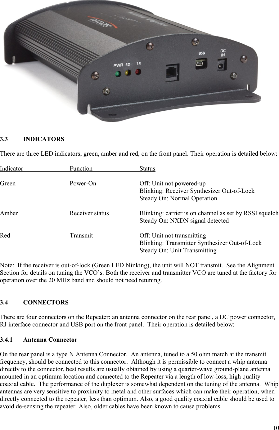
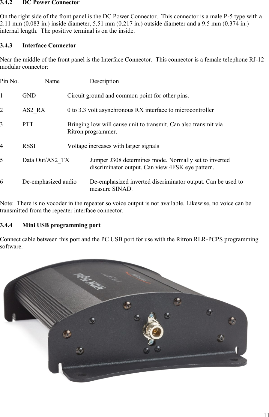
>
Ritron
>
RIT44 465 User Manual
User Manual
Navigation menu
Upload a User Manual
Namespaces
Wiki Guide
HTML
PDF
Info
Views
User Manual
Discussion / Help
Navigation