Ritron RIT44-465 UHF-DIGITAL REPEATER User Manual TYPE OF EXHIBIT
Ritron Inc UHF-DIGITAL REPEATER TYPE OF EXHIBIT
Ritron >
User Manual
1
Pub. RLR-465 MRM
10 April 2018
RLR-465NX
BY RITRON
PROGRAMMABLE NXDN 10W REPEATER
MAINTENANCE/REPAIR/OPERATING MANUAL
FOR USE BY AUTHORIZED SERVICE/MAINTENANCE PERSONNEL ONLY
2
Table of Contents
Pub. RLR-465 MRM .............................................................................................................................. 1
RLR-465NX ........................................................................................................................................... 1
PROGRAMMABLE NXDN 10W REPEATER ............................................................................................ 1
1. SPECIFICATIONS ................................................................................................................................ 3
2. INTRODUCTION .................................................................................................................................. 4
2.1 GENERAL .................................................................................................................................... 4
2.2 INSPECTION ............................................................................................................................... 4
2.3 MODEL IDENTIFICATION ....................................................................................................... 4
2.4 FCC REGULATIONS .................................................................................................................. 4
2.5 RF SAFETY ISSUES ................................................................................................................... 4
2.6 RITRON, INC. LIMITED WARRANTY..................................................................................... 7
3. OPERATION ......................................................................................................................................... 9
3.1 GENERAL OPERATION ............................................................................................................ 9
3.2 DUTY CYCLE/TEMPERATURE LIMITS ................................................................................. 9
3.3 INDICATORS .............................................................................................................................10
3.4 CONNECTORS ...........................................................................................................................10
3.4.1 Antenna Connector ..................................................................................................................10
3.4.2 DC Power Connector ...............................................................................................................11
3.4.3 Interface Connector .................................................................................................................11
3.4.4 Mini USB programming port ...................................................................................................11
4. REPEATER FEATURES ......................................................................................................................12
4.1 PROGRAMMING SETUP ..........................................................................................................12
4.2 COMPUTER SOFTWARE COPYRIGHTS ...............................................................................12
5. THEORY OF OPERATION .................................................................................................................12
5.1 DUPLEXER .................................................................................................................................13
5.2 RECEIVER ..................................................................................................................................13
5.2.1 Front-End .................................................................................................................................13
5.2.2 1st IF .........................................................................................................................................13
5.2.3 2nd IF Sub-System ....................................................................................................................13
5.2.4 1ST Local Oscillator/Receive Synthesizer ................................................................................14
5.2.5 2ND Local Oscillator .................................................................................................................14
5.2.6 Base band data .........................................................................................................................14
5.3 TRANSMITTER ..........................................................................................................................14
5.3.1 Transmit Synthesizer ...............................................................................................................14
5.3.2 RF Power Amplifier Stages .....................................................................................................15
5.3.3 Transmitter signaling ...............................................................................................................15
5.4 POWER DISTRIBUTION ...........................................................................................................15
5.5 MICROCONTROLLER ..............................................................................................................15
6. FACTORY ALIGNMENT ....................................................................................................................16
6.1 DUPLEXER .................................................................................................................................16
6.2 RECEIVER ..................................................................................................................................17
6.2.1 RX VCO Band adjustment and reference Oscillator tuning ....................................................17
6.2.2 RX filter alignment and Sensitivity .........................................................................................17
6.2.3 2nd IF local oscillator trimming for minimum filter distortion .................................................17
6.2.4 Squelch ....................................................................................................................................17
6.3 TRANSMITTER ..........................................................................................................................18
6.3.1 TX frequency adjustment ........................................................................................................18
6.3.2 TX VCO Band, Modulation Balance and Deviation adjustment .............................................18
6.3.4 TX power adjustment ..............................................................................................................18
3
1. SPECIFICATIONS
1.1 GENERAL
Modulation format NXDN Super Narrowband
Frequency Range 450-470 MHz
FCC ID AIERIT44-465
IC ID 1084A-RIT44465
RX/TX Separation: 5 MHz
Operational Bandwidth
Duplexer 50 kHz
Receiver and Transmitter 20 MHz
Synthesizer Step Size 6.25 kHz
Channels 1
Power Requirements
Receive 130mA at 13.8 VDC
Transmit:
5 watt maximum output 10 VDC nominal @ 2.0A
8 watt maximum output 12 VDC regulated @ 2.4A
10 watt maximum output 13.8 VDC regulated @ 2.8A
TX Timeout Timer 0-34 min, programmable by PC
Analog CW Morse Code Interval Timer 0-34 min, programmable by PC
Front Panel I/O Connector RJ-12
Programming port Mini USB
RF Connector Type N
Front Panel Indicators 1 Power Green LED
1 RX Amber LED
1 TX Red LED
Antenna Impedance 50 ohms resistive, VSWR 1.5:1 or less
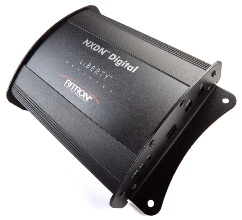
Dimensions 8”L x 5.75”W x 2.125” H
Weight 3.5 lbs.
Operating Temperature Range -30C to +50C
1.2 RECEIVER (At antenna connector)
Sensitivity 0.3 uV
Adjacent Channel Selectivity 40 dB (6.25 kHz offset with 1.3 kHz jammer deviation)
Spurious Response Rejection 75 dB
Image Rejection 90 dB
Intermodulation Rejection 73 dB
Frequency Stability 1.0 ppm
1.3 TRANSMITTER (At antenna connector)
Output Power 2 to 10 watts programmable
Duty Cycle 100% up to +30C (degraded linearly to 10% at +50C)
Frequency Stability 1.0 ppm
Spurious and Harmonics -25 dBm
4
2. INTRODUCTION
2.1 GENERAL
The RITRON RLR-465NX NXDN repeater is a synthesized table-top UHF repeater that operates in the
450 to 470 MHz FM communications band. This repeater is designed to handle super narrow band 6.25
kHz NXDN signals only. Its maximum output power level is 10 watts. Depending upon the type of power
supply which is available to power the unit it can be programmed for power output from 2 to 10 Watts. The
unit receives signals originating from handheld, mobile, or fixed stations on one frequency and
simultaneously retransmits the signals on a second frequency. This type of operation is described as full
duplex. The unit contains an integral duplexer which allows a single antenna to be used for simultaneous
transmission and reception. Full duplex operation with a repeater enables mobile and handheld units to
communicate over much greater distance than is possible without a repeater. The Repeater is designed to
be powered from an external DC power source. It draws about 140 mA in RX mode making it ideal for use
with a 12 volt lead acid battery.
The received NXDN signal is demodulated and is error corrected. The retransmitted signal is thus cleaned
up and received noise is not repeated as in a conventional analog repeater. All NXDN signals received can
be repeated. However, if the operator chooses, only specific received RAN codes are allowed to repeat. A
table of up to 10 RAN codes allows filtering of what can be repeated.
2.2 INSPECTION
Inspect the unit immediately after delivery and report any damages to the shipping company. The repeater
package should contain:
RLR-465NX repeater
RPS-3000 3Amp 13.8 VDC power supply
DC power supply cable
RLR-PCPS programing software
2.3 MODEL IDENTIFICATION
The Repeater’s model, serial number, and FCC identification number appear on a label attached to the rear
panel.
2.4 FCC REGULATIONS
The Federal Communications Commission (FCC) requires that the radio owner obtain a station license
before using the equipment to transmit. The user is not required to obtain an operating license. The station
licensee is responsible for proper operation and maintenance of his radio equipment and for ensuring that
transmitter power, frequency, and occupied bandwidth are within the limits specified by the station license.
This is effected by aligning the unit per the instructions in the Alignment section of this manual as well as
periodically checking that transmitter and deviation. Because the RLR-465NX contains a transmitter, THE
REPEATER MUST BE LICENSED BEFORE USE. A RITRON dealer can help with obtaining an FCC
license. There are no user adjustments available inside this product. All alignment steps and adjustments
including programming frequency, trimming frequency, setting modulation and power must be performed
by a qualified two-way radio technician. The programming software and hardware is available only to
RITRON authorized radio dealers and must not be made available to the end user.
2.5 RF SAFETY ISSUES
On August 25, 1997, the FCC adopted the second of two Orders finalizing its rules regarding compliance
with safety limits for human exposure to radio frequency (RF) emissions. All transmitting facilities,
operations and devices regulated by the FCC, including this product, must be in compliance with the RF
exposure limits contained in Code of Federal Regulations (CFR) 47 parts 1.1307(b)(1)-(b)(3). It is the
responsibility of the licensee or grantee to either take action to bring the facility, operation or device into
5
compliance or file an Environmental Assessment with the FCC. The following precautions should be taken
with regard to the use of this equipment:
PLEASE NOTE THE FOLLOWING WITH REGARD TO RF EXPOSURE FOR THIS PRODUCT,
EXPOSURE TO RADIO FREQUENCY ENERGY:
This product generates radio frequency (RF) energy when transmitting. This product has been evaluated for
compliance with the maximum permissible exposure limits for RF energy at the maximum power rating of
the unit. To meet the minimum separation distance and keep the maximum RF exposure at or below the
General Population/Uncontrolled limits in the country of use the table below to determine the minimum
distances. This product is not to be used by the general public in an uncontrolled environment unless
compliance with the Uncontrolled/General Population limits for RF exposure can be assured.
The receiver section of this device complies with Industry Canada license-exempt RSS standard(s).
Operation is subject to the following two conditions: (1) this device may not cause interference, and (2) this
device must accept any interference, including interference that may cause undesired operation of the
device.
This radio transmitter (RLR-465) has been approved by Industry Canada to operate with the antenna types
listed below with the maximum permissible gain and required antenna impedance for each antenna type
indicated. Antenna types not included in this list, having a gain greater than the maximum gain indicated
for that type, are strictly prohibited for use with this device.
The following 50 ohm antenna types can be used with the RLR-465:
Canadian
USA
Minimum
Minimum
Antenna
Antenna
Distance
Distance
Type
Gain(dBi)
(m)
(m)
Yagi
12
2.72
2.05
High gain Omni
10
2.16
1.63
5/8 wavelength
3
0.97
0.73
Quarter wave
2
0.86
0.65
Veuillez NOTER CE QUI SUIT À L'ÉGARD DE L'exposition aux RF SUR CE PRODUIT :
Ce produit génère de l'énergie radiofréquence (RF) lors de la transmission. Ce produit a été évalué pour la
conformité aux limites d'exposition maximales admissibles pour l'énergie RF à la puissance nominale
maximale de l'unité. Pour respecter la distance de séparation minimale et maintenir l'exposition maximale
aux fréquences radioélectriques égale ou inférieure aux limites de la population générale / non contrôlée du
pays d'utilisation, le tableau ci-dessous permet de déterminer les distances minimales. Ce produit ne doit
pas être utilisé par le grand public dans un environnement non contrôlé, sauf si les limites de la population
générale / non contrôlée pour l'exposition aux radiofréquences peuvent être respectées.Des gains plus
élevés que les antennes avec un dipôle sont capables de générer des champs dans la partie la plus solide de
leur domaine et, par conséquent, exigent une plus grande séparation de l'antenne. Ils peuvent être montés
plus haut que l'unité de répétition qui feront augmenter la séparation de l'opérateur de l'antenne. Ce produit
n'est pas d'être utilisées par le grand public dans un environnement non contrôlé à moins que le respect de
la population générale/incontrôlée des limites pour l'exposition aux RF peuvent être assurés.
Le récepteur de ce présent appareil est conforme aux CNR d'Industrie Canada applicables aux appareils
radio exempts de licence. L'exploitation est autorisée aux deux conditions suivantes : (1) l'appareil ne doit
pas produire de brouillage, et (2) l'utilisateur de l'appareil doit accepter tout brouillage radioélectrique
subi, même si le brouillage est susceptible d'en compromettre le fonctionnement.
Le présent émetteur radio (RLR-465) a été approuvé par Industrie Canada pour fonctionner avec les types
d'antenne énumérés ci-dessous et ayant un gain admissible maximal et l'impédance requise pour chaque

6
type d'antenne. Les types d'antenne non inclus dans cette liste, ou dont le gain est supérieur au gain
maximal indiqué, sont strictement interdits pour l'exploitation de l'émetteur.
Les types d'antenne de 50 ohms peut être utilisé avec le RLR-465 :
Canadian
USA
Minimum
Minimum
Antenna
Antenna
Distance
Distance
Type
Gain(dBi)
(m)
(m)
Yagi
12
2.72
2.05
High gain Omni
10
2.16
1.63
5/8 wavelength
3
0.97
0.73
Quarter wave
2
0.86
0.65
To limit exposure to RF energy to levels below the limit, please observe the following:
DO NOT OPERATE THIS EQUIPMENT unless all RF connectors are secure and any open
connectors are properly terminated.
GROUND ALL RADIO EQUIPMENT.
ALLOW ONLY QUALIFIED SERVICE PERSONNEL to service this product.
DO NOT ALLOW THIS EQUIPMENT to be set to power levels above its design limit or the licensed
maximum.
When used as directed, this series of radios is designed to comply with the FCC’s and Industry Canada’s
RF exposure limits for “Uncontrolled/General Population”. In addition, they are designed to comply with
the following Standards and Guidelines:
• United States Federal Communications Commission, Code of Federal Regulations; 47 CFR §§ 2 sub-
part J.
• American National Standards Institute (ANSI) / Institute of Electrical and Electronic Engineers (IEEE)
C95. 1-1992.
• Institute of Electrical and Electronic Engineers (IEEE) C95.1-1999 Edition.
Copyright Telecommunications Industry Association

7
2.6 RITRON, INC. LIMITED WARRANTY
RITRON, INC. ("RITRON") provides the following warranty against defects in materials and/or workmanship in this
RITRON Liberty Repeater and its Accessories under normal use and service during the applicable warranty period (as
stated below). "Accessories" means original power supply, antennas, cables and items contained in the programming
and programming/service kits.
WHAT IS COVERED FOR HOW LONG WHAT RITRON WILL DO
RLR-456 Digital Repeater 1 year During the first year after date of purchase, RITRON® will
repair or replace the defective product, at RITRON's
option, parts and labor included at no charge.
Accessories 90 days 90 days after date of purchase
WHAT THIS WARRANTY DOES NOT COVER:
• Any technical information provided with the covered product or any other RITRON products;
• Installation, maintenance or service of the product, unless this is covered by a separate written agreement with
RITRON;
• Any products not furnished by RITRON which are attached or used with the covered product, or defects or damage
from the use of the covered product with equipment that is not covered (such as defects or damage from the charging or
use of batteries other than with covered product):
• Defects or damage, including broken antennas, resulting from:
- misuse, abuse, improper maintenance, alteration, modification, neglect, accident or act of God,
- the use of covered products other than in normal and customary manner or,
- improper testing or installation;
• Defects or damages from unauthorized disassembly, repair or modification, or where unauthorized disassembly,
repair or modification prevents inspection and testing necessary to validate warranty claims;
• Defects or damages in which the serial number has been removed, altered or defaced.
• Batteries if any of the seals are not intact.
IMPORTANT: This warranty sets forth the full extent of RITRON’s express responsibilities regarding the covered
products, and is given in lieu of all other express warranties. What RITRON has agreed to do above is your sole and
exclusive remedy. No person is authorized to make any other warranty to you on behalf of RITRON. Warranties
implied by state law, such as implied warranties of merchantability and fitness for a particular purpose, are limited to
the duration of this limited warranty as it applies to the covered product. Incidental and consequential damages are not
re-coverable under this warranty (this includes loss of use or time, inconvenience, business interruption, commercial
loss, lost profits or savings). Some states do not allow the exclusion or limitation of incidental or consequential
damages, or limitation on how long an implied warranty lasts, so the above limitations or exclusions may not apply to
you. Because each covered product system is unique, RITRON disclaims liability for range, coverage, or operation of
the system as a whole under this warranty
.
WHO IS COVERED BY THIS WARRANTY: This warranty is given only to the purchaser or lessee of covered
products when acquired for use, not resale. This warranty is not assignable or transferable.
HOW TO GET WARRANTY SERVICE: To receive warranty service, you must deliver or send the defective
product, delivery costs and insurance prepaid, within the applicable warranty period, to RITRON, INC., 505 West
Carmel Drive, Carmel, Indiana 46032, Attention: Warranty Department. Please point out the nature of the defect in as
much detail as you can. You must retain your sales or lease receipt (or other written evidence of the date of purchase)
and deliver it along with the product. If RITRON chooses to repair or replace a defective product, RITRON may re-
place the product or any part or component with reconditioned product, parts or components. Replacements are covered
for the balance of the original applicable warranty period. All replaced covered products, parts or components become
RITRON’s property.
RIGHTS TO SOFTWARE RETAINED: Title and all rights or licenses to patents, copyrights, trademarks and trade
secrets in any RITRON software contained in covered products are and shall remain in RITRON. RITRON
nevertheless grants you a limited non-exclusive, transferable right to use the RITRON software only in conjunction
with covered products. No other license or right to the RITRON software is granted or permitted.
YOUR RIGHTS UNDER STATE LAW: This warranty gives you specific legal rights, and you may also have other
rights which vary from state to state.
8
WHERE THIS WARRANTY IS VALID: This warranty is valid only within the United States, the District of
Columbia and Puerto Rico.
9
3. OPERATION
3.1 GENERAL OPERATION
Test the Repeater for proper operation as the unit is received before attempting to reprogram and/or retune
it. There is no On/Off switch on the unit; it is powered up when a power supply is connected. Standard
factory programming is a receive frequency of 469.500 MHz and a transmit frequency of 464.500 MHz.
Custom set up can be requested from the factory.
Retune the internal duplexer if either the receive or transmit frequency are to be changed by more than 50
kHz. Note that the nominal transmit/receive spacing is 5 MHz for this product. Larger spacing may be
accommodated, but not smaller. See the Alignment section.
The Repeater is setup to accept a 13.8 volt/3amp RITRON RS-4A regulated source of power and can
provide up to 10 watts of output power at the antenna connector. See the duty cycle/temperature limits
below. The transmitter power output at the antenna connector can be programmed to vary from 2 watts to
the 10 watts. Ten Watts can only be realized by using at least a 13.8 volt source. If operating from a
nominal 12 volt lead acid battery the power will be somewhat lower depending on the voltage.
The RLR-465NX has a standard frequency separation of 5 MHz between transmit and receive. The normal
configuration is for the receive frequency to be above the transmit frequency. “Inverted” systems are
reversed with the transmit frequency higher than the receive frequency. The cables on the duplexer are
long enough to allow them to be swapped. Normally, the duplexer cables are tie-wrapped in a loop. The
tie-wraps can be cut to allow swapping the connections.
Unlike an analog repeater there is no transmitter “hang time”. This allows lower duty cycle operation
keeping the unit cooler since the transmitter turns off when there is no speech. The analog “hang time” kept
the repeater transmitter up for a number of seconds after speech to eliminate squelch tails and allow only
certain people repeater access. There is no squelch tails in digital communications.
3.2 DUTY CYCLE/TEMPERATURE LIMITS
Due to internal heating of the RF transmitter components, there is a limit on the maximum duty cycle of the
repeater depending upon temperature and output power. The repeater is designed for 100% duly cycle at 25
C or below. It should be linearly de-rated to 10% at 50 C. Lower power settings will improve this
slightly. Also adjusting the final FET output matching cap for minimum current drain while transmitting
will reduce heat generation. Once the PCB reaches 55 C the repeater will power down to 2 Watts. Full
power operation will resume when the temperature falls to 52 C. If the repeater temperature reaches 60 C
the repeater will shut down.
Usage data is available on the “Usage” tab. Amongst other data it logs the six warmest repeater “events”.
An “event” or conversation starts when at least 2 minutes of no transmission has occurred on the repeater.
This data informs the operator of start and stop temperatures as well as conversation durations and
transmitter duty cycle usage.
10
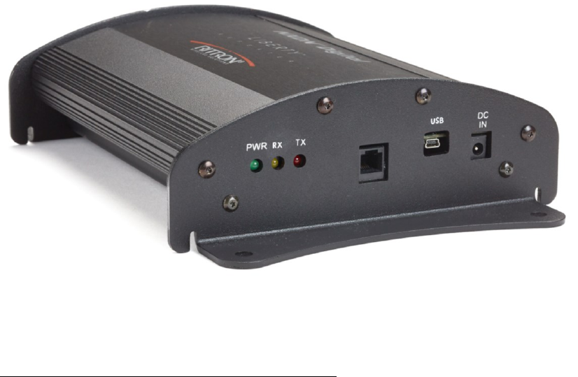
3.3 INDICATORS
There are three LED indicators, green, amber and red, on the front panel. Their operation is detailed below:
Indicator Function Status
Green Power-On Off: Unit not powered-up
Blinking: Receiver Synthesizer Out-of-Lock
Steady On: Normal Operation
Amber Receiver status Blinking: carrier is on channel as set by RSSI squelch
Steady On: NXDN signal detected
Red Transmit Off: Unit not transmitting
Blinking: Transmitter Synthesizer Out-of-Lock
Steady On: Unit Transmitting
Note: If the receiver is out-of-lock (Green LED blinking), the unit will NOT transmit. See the Alignment
Section for details on tuning the VCO’s. Both the receiver and transmitter VCO are tuned at the factory for
operation over the 20 MHz band and should not need retuning.
3.4 CONNECTORS
There are four connectors on the Repeater: an antenna connector on the rear panel, a DC power connector,
RJ interface connector and USB port on the front panel. Their operation is detailed below:
3.4.1 Antenna Connector
On the rear panel is a type N Antenna Connector. An antenna, tuned to a 50 ohm match at the transmit
frequency, should be connected to this connector. Although it is permissible to connect a whip antenna
directly to the connector, best results are usually obtained by using a quarter-wave ground-plane antenna
mounted in an optimum location and connected to the Repeater via a length of low-loss, high quality
coaxial cable. The performance of the duplexer is somewhat dependent on the tuning of the antenna. Whip
antennas are very sensitive to proximity to metal and other surfaces which can make their operation, when
directly connected to the repeater, less than optimum. Also, a good quality coaxial cable should be used to
avoid de-sensing the repeater. Also, older cables have been known to cause problems.
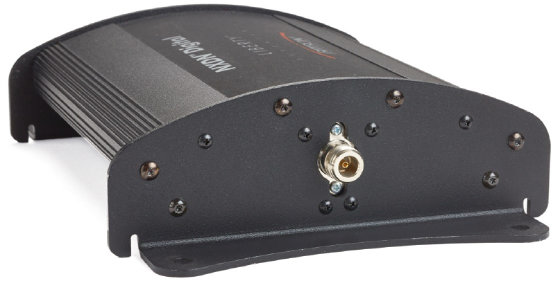
11
3.4.2 DC Power Connector
On the right side of the front panel is the DC Power Connector. This connector is a male P-5 type with a
2.11 mm (0.083 in.) inside diameter, 5.51 mm (0.217 in.) outside diameter and a 9.5 mm (0.374 in.)
internal length. The positive terminal is on the inside.
3.4.3 Interface Connector
Near the middle of the front panel is the Interface Connector. This connector is a female telephone RJ-12
modular connector:
Pin No. Name Description
1 GND Circuit ground and common point for other pins.
2 AS2_RX 0 to 3.3 volt asynchronous RX interface to microcontroller
3 PTT Bringing low will cause unit to transmit. Can also transmit via
Ritron programmer.
4 RSSI Voltage increases with larger signals
5 Data Out/AS2_TX Jumper J308 determines mode. Normally set to inverted
discriminator output. Can view 4FSK eye pattern.
6 De-emphasized audio De-emphasized inverted discriminator output. Can be used to
measure SINAD.
Note: There is no vocoder in the repeater so voice output is not available. Likewise, no voice can be
transmitted from the repeater interface connector.
3.4.4 Mini USB programming port
Connect cable between this port and the PC USB port for use with the Ritron RLR-PCPS programming
software.
12
4. REPEATER FEATURES
The RLR-465NX repeater may be programmed with a transmit frequency, receive frequency, and a number
of other features:
Transmit time-out timer This feature determines how long the unit may transmit continuously
before the transmitter automatically shuts off. It is delivered from the
factory as “0” meaning no time out.
Morse code identifier The repeater can be programmed to transmit a Morse code identifier
at a specified time interval as required by the FCC
RAN The repeater can be set up to repeat all NXDN traffic.
It can also be set up to allow up to only 10 unique RAN codes.This
helps eliminate a inadvertent NXDN on channel signal from triggering
the repeater.
Low Voltage voice alert When the input voltage to the repeater falls below 11 volts the repeater
will transmit an NXDN voice message alerting users to a low battery
condition. This alert will repeat every 30 minutes until the voltage
recovers. A custom voice message can be writen using a portable radio
by clicking “Record Low voltage Voice” and then PTTing the portable
while speaking the message. This alert voice message can have a RAN
code and/or source and destination ID so as to target a specific radio
such as the system operator.
High temperature operation The RLR-465NX has sufficient heatsinking to allow the repeater to
work continuously at temperatures of 25 degrees Celsius or below. At
higher temperatures with prolonged usage the thermal sensor on the
PCB will sense an excessive temperature at 55 C and reduce power
output to 2 Watts. A power of 10 Watts will resume when the
temperature falls below 52 C. A temperature of 60 C will shut the
transmitter down until temperature cools to 59 C and resume 2 Watts.
4.1 PROGRAMMING SETUP
RITRON programming kit RLR-PCPK supports programming the RLR-465NX repeater using a PC
compatible computer. To use the programming software, connect the Repeater to the computer USB port
of the PC. The software includes on-screen instructions and Help files.
4.2 COMPUTER SOFTWARE COPYRIGHTS
The RITRON, Inc. products described in this manual include copyrighted RITRON, Inc. computer
programs. Laws in the United States and other countries grant to RITRON, Inc. certain exclusive rights in
its copyrighted computer programs, including the exclusive right to distribute copies of the programs, make
reproductions of the programs, and prepare derivative works based on the programs. Accordingly, any
computer programs contained in RITRON, Inc. products may not be copied or reproduced in any manner
without the express written permission of RITRON. The purchase of RITRON, Inc. products does not
grant any license or rights under the copyrights or other intellectual property of RITRON, Inc., except for
the non-exclusive, royalty-free license to use that arises in the sale of a product, or as addressed in a written
agreement between RITRON, Inc. and the purchaser of RITRON, Inc. products.
5. THEORY OF OPERATION
This repeater is designed to handle super narrow band 6.25 kHz NXDN. It will receive on one frequency
and transmit on another a nominal 5 MHz offset. It has no voice vocoder so it cannot receive voice on a
13
speaker or transmit voice from a microphone. It is designed to operate at 13.8 VDC to yield 10 Watts
output. The repeater can be set up to repeat all super narrowband signals on the receive frequencies or be
set up via a table to repeat only certain RAN codes. For further explanation see the RITRON programmer
and help file. The unit draws about 140 mA in receive mode and about 3 Amps in transmit mode. This
allows it to be battery operated or battery backed up.
5.1 DUPLEXER
The duplexer allows for simultaneous transmission and reception of RF signals. There is a receive path and
a transmit path which connect to the RF input and output of the main PCB and a common point at the
antenna connector.
In the receive path is a two-cavity notch filter. This filter allows the receive signal from the antenna
connector to pass through with about 1.5 dB loss, but notches the transmitter RF output signal by 70 dB or
more to prevent overloading the receiver. The transmit path also contains a two-cavity notch filter, this one
tuned to the receive frequency. This filter removes transmitter noise which exists at the receive frequency
and which would interfere with the desired receive signal, if not removed. This filter has about 1.75 dB
loss. Because the notches are very narrow, the duplexer must be re-tuned if the frequency of operation is
changed by more than 50 kHz. If the repeater receive frequency is lower than the transmit frequency then
these two notch filters are physically reversed. The coaxial connectors will cross if this is the case. The low
pass filter, which is physically next to the transmitter connector, will be routed to the receive connector and
the high pass filter, next to the receive connector, will be routed to the transmit connector.
5.2 RECEIVER
5.2.1 Front-End
The receiver front-end comprises the RF amplifier stages with associated filters and the first mixer. The
input signal from the J101 (RX IN) passes through a two resonator bandpass filter formed around L101 and
L102. This filter is narrow enough at 10 MHz to protect the receive RF amplifier, but wide enough to keep
its insertion loss low at 2 dB. This filter stage is followed by the RF amplifier. The RF amplifier stage has
a gain of about 12 dB and a noise figure of 1.5 dB. This stage, along with the first filter, are largely
responsible for the sensitivity of the Repeater. The RF amplifier is followed by a two resonator bandpass
filter formed around L103 and L104. This filter is somewhat narrower than the two-pole filter and thus has
a higher insertion loss at 7 dB. The total filtering action is to limit the number of off-channel interfering
signals that the receiver might be exposed to and to remove signals at the spurious response frequencies of
the mixer which follows. More amplification through Q102 is needed to overcome this second filter section
insertion loss.
The job of the 1st mixer, U101 is to convert signals at the receive frequency to that of the 1st IF at 43.65
MHz. It does this by mixing the 1st local oscillator signal at a frequency 43.65 MHz below that of the
desired receive frequency to the IF frequency of 43.65 MHz. The 43.65 MHz output of U101 exits through
T102 and is routed to the 1st IF filter. U101 has a conversion gain of 2 dB and a noise figure of 10 dB.
This performance in combination with the front-end RF amplifier stages determines the sensitivity of the
receiver.
5.2.2 1st IF
The 1st IF stage consists of two two-pole monolithic crystal filters separated by an amplifier. The two
filters are FL101 and FL102. These filters are bandpass in response with a bandwidth of 4 kHz and an
insertion loss of 1.5 dB. To overcome the losses of the filters and to prevent interaction between them, they
are separated by an amplifier formed around Q109.
5.2.3 2nd IF Sub-System
14
IC U102 is responsible for converting signals at the 1st IF to the 2nd IF where additional filtering and
amplification take place. The 43.65 MHz signals enters U102 at pin 16. It is then mixed with the 2nd local
oscillator signal at pin 1 to product a signal at the 2nd IF of 450 kHz at pin 3. The 2nd IF signal at pin 3 is
filtered by the FL103, the 2nd IF filter. This filter is a bandpass filter with a bandwidth of 4 kHz and an
insertion loss of 5 dB. The output of the filter re-enters U102 at pin 5 where it is amplified and then limited
to remove amplitude modulation components. The limited signal is then mixed against a 90 phase shifted
version of itself and filtered by Y101. This acts as an FM demodulator. The demodulated output exits
U102 at pin 9.
5.2.4 1ST Local Oscillator/Receive Synthesizer
The local oscillator signal for the 1st mixer is generated by the receive synthesizer. The receive synthesizer
is based around a voltage controlled oscillator (VCO) and a synthesizer sub-system IC which handles the
digital portion of the synthesizer. The voltage controlled oscillator is an oscillator whose frequency can be
controlled by a voltage. The receive voltage controlled oscillator is formed around Q107 with varactor
diode D101 and D102 electronically controlling the frequency. A sample of the oscillator frequency is
sampled by R124 and C160 and sent to U104, an integrated monolithic Phase-Locked Loop (PLL)
synthesizer IC. Inside U104, the VCO frequency is divided by programmable digital dividers to a
frequency in the 50 kHz range. FL104, the 36.4 MHz receive reference oscillator’s frequency is also
divided down to the 50 kHz range. A phase/frequency detector compares the two divided down
frequencies and generates an error signal at U104, pin 2 which is filtered and used to pull the VCO on
frequency. By controlling the VCO divider number, the locked frequency can be changed. The divider
numbers are loaded into U104 by the microprocessor. The 20 MHz tuning range of the VCO is set by
C150. Because the VCO is locked to the receive reference oscillator, FL104, the frequency stability of
FL104 determines the frequency stability of the VCO and thus the 1st local oscillator.
The output of the VCO is amplified by Q104 and Q106 to about 5 dBm to drive the 1st mixer. For
alignment purposes, a sample of the 1st local oscillator is available at TP101. For proper mixing operation,
the VCO is made to oscillate at a frequency 43.65 MHz below the receive frequency.
5.2.5 2ND Local Oscillator
To convert the 1st IF signals at 43.65 MHz to the 2nd IF frequency of 450 kHz, requires a 2nd local oscillator
frequency of 43.2 MHz (43.65 – 0.450). This is created by multiplying the 14.4 MHz output frequency of
FL105 by three in Q103.
5.2.6 Base band data
Discriminator audio from U102 passes to U103-C and it is amplified and through U103-D where is
equalized. It is then sent to the NXDN decoder IC U302 for demodulation. The main controller U301 reads
the data and performs needed tasks such as error correction, RAN and ID decoding.
5.3 TRANSMITTER
5.3.1 Transmit Synthesizer
The transmit synthesizer operates similar to the receive synthesizer except that the oscillator is locked to
the transmit frequency rather than offset by the 1st IF frequency. The transmit VCO is formed around Q207
and electronically tuned by D202 and D203. The oscillator frequency is sampled by R227 and C226 and
routed to U201, the transmit synthesizer IC. The oscillator frequency is divided down around 50 kHz and
compared in phase and frequency to the divided transmit reference oscillator signal. The error signal is
filtered and sent to the varactor diode D202 and D203 to lock the VCO on frequency. The reference is
created by dividing down the transmit reference oscillator frequency of 36.4 MHz from FL201. To
modulate the transmitter, the VCO must allow for frequency modulation other than what is required to put
it on frequency. This is effected by D204. The 20 MHz tuning range tuning range of the VCO is set by
15
C296. Q212 is an electronic switch which keeps the transmit VCO turned off when the unit is not
transmitting.
5.3.2 RF Power Amplifier Stages
The output of the VCO buffer stage, Q205 is at a level of about 5 dBm. This is amplified to the 2 to 10
watt level by Q201, Q202, Q203, and Q204. Q210 allows the first two amplifier stages to be turned on
after the transmit VCO is locked and on frequency. After this the RF power output is ramped up by
increasing the bias voltage on the last two FETs. The output power can be adjusted by programmer and the
voltage appears at pin 9 of U203-C, which sets the bias voltage on the current control loop. This current
control loop formed by current sensor Q211 and op-amp U202 maintain the FET final (Q201) current. As
the gain of the driver stages change due to temperature the current loop keeps the power steady. It does this
by changing the FET bias on the final two FETs Q202 and Q201. Q201 is followed by an impedance
matching network and a low-pass filter to remove transmitter frequency harmonics. This amplifier can
output about 15 Watts into the duplexer which dissipates 4 to 5 Watts when a full 10 Watts is needed.
5.3.3 Transmitter signaling
Once a transmit NXDN packet is ready the main microcontroller U301 will send it to the transmitter
NXDN modulator IC U303. It sends the NXDN 4FSK signal out pin 23 via the TX_MOD line. The
TX_MOD line is sent to a summing amplifier U205-C. Also summed into the amp is the Morse code ID
signal CWID from the microcontroller. The CWID is fed through a 5-pole low-pass filter which removes
audio harmonics and keeps the signal within FCC occupied bandwidth limits. After the summing amplifier
the NXDN signal is sent through a deviation pot U204-C and then through a summing amplifier which
trims the reference oscillator bias voltage to bring the RF carrier on frequency. The last pot to go through is
the balance pot U203-B which adjusts the VCO modulating signal level to form a nice “eye” pattern.
5.4 POWER DISTRIBUTION
Power enters the unit through J601 and is protected from reverse voltage by D601 through D604 diodes.
The 4 Amp fuse will blow if either a short or reverse polarity on the supply exists. A 6 volt switching
power supply exists to reduce current consumption both in receive mode and in transmit mode. This keeps
the unit cooler by eliminating excess power dissipation in voltage regulators.
5.5 MICROCONTROLLER
U301 controls the following radio functions:
1) USB programming of the radio via J302.
2) NXDN packet handling and FEC error correction through U302 and U303.
3) Radio status indicators via RED, AMBER and GREEN LEDs.
4) PCB temperature monitoring via U609. Causes “overheat” shut back when too hot.
5) Power supply under voltage monitoring via U103-B. Useful when a battery only supply is used.
6) Low voltage voice message and can be programmed via RITRON programmer and portable radio.
7) Sends CW ID periodically. Programmable 1 to 34 minutes.
8) Loads RX and TX frequency synthesizers as well as deviation, balance and frequency trim pots.
16
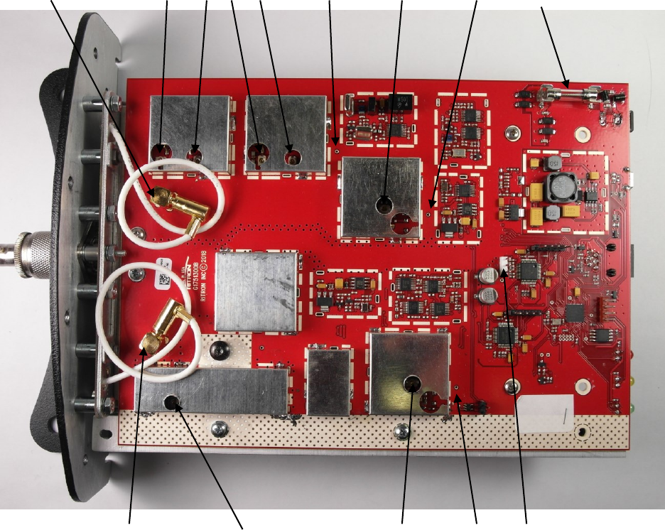
RX SMB connector RX BPF tuning caps TP101 RX VCO C150 TP102 4 Amp fuse
TX SMB connector RF power adj C206 TX VCO C296 TP201 J308
6. FACTORY ALIGNMENT
6.1 DUPLEXER
Tuning the duplexer requires either a network analyzer or an accurate RF signal generator and low level RF
detector. If the customer uses a repeater transmit frequency that is lower than the receive frequency the
coaxial cable connections are direct. That is to say, the transmit duplexer cavities are directly below the
transmitter and the receive duplexer cavities are below the receiver section. Otherwise the cables will cross
each other when connected to the RF board.
1) Disconnect power from the repeater. Disconnect SMB coaxial connectors from the RF board.
Inserting a flat screw drive between the connector parts and twisting will aid in releasing the cable.
Do not pull on the cable base as this could damage the cable. Connect SMB adapters and coaxial
cables to test instrument. If desired test equipment can go through both duplexers at once. This
will produce notches at two frequencies 5 MHz apart.
2) To adjust transmit duplexer to notch receive frequency where TX frequency is below RX
frequency, set or look at response at receive frequency. Adjust screws under transmitter to
minimize response at RX frequency.
17
3) To adjust transmit duplexer to notch TX frequency where TX frequency is below RX frequency,
set or look at response at transmit frequency. Adjust screws under receiver to minimize response at
TX frequency.
4) Tighten nuts when finished.
6.2 RECEIVER
6.2.1 RX VCO Band adjustment and reference Oscillator tuning
1) Go to the “Alignment” tab and click “Frequency/Power” then “Center Frequency Adjustment”.
This will load a 425 MHz local oscillator frequency into the RX synthesizer.
2) Adjust the C150 band shifting cap to yield a 3.8 +/- 0.2 VDC tuning voltage on TP102. The RX
band will now operate anywhere in the 20 MHz RX band after being programmed to that
frequency by the RITRON programmer. The VCO tuning voltage will range from about 1 volt at
450 MHz to 4 volts at 470 MHz.
3) Connect probe to the receiver local oscillator test point TP101 and measure the 425 MHz
frequency. Perform next three steps if more than +/- 200 Hz off.
4) “Center Frequency Adjustment”: adjust “RX Freq Trim” to yield 425 MHz +/- 50 Hz
5) “Frequency Positive Correction Factor”: adjust “RX Freq Trim” to yield 425 MHz +/- 50 Hz
6) “Frequency Negative Correction Factor”: adjust “RX Freq Trim” to yield 425 MHz +/- 50 Hz. The
36.4 MHz RX reference crystal is now calibrated. Click “Program Repeater” to save.
7) Click the “Main” tab to return to the repeater’s programmed RX frequency. The VCO tuning
voltage will change to correspond to that frequency.
6.2.2 RX filter alignment and Sensitivity
1) Connect receive duplexer cable to RX port (J101). Set signal generator to -118 dBm with 1.5 kHz
deviation on a 1 kHz tone and connect to duplexer antenna port.
2) Connect oscilloscope and SINAD meter to pin 6 of RJ-12 connector. This is the de-emphasized
output.
3) Adjust C102, C108, C115 and C121 to maximize SINAD. Signal generator can be temporarily set
higher if need be to see 1 kHz sine wave. Unit should obtain at least -118 dBm sensitivity for a 12
dB SINAD when tuned up.
6.2.3 2nd IF local oscillator trimming for minimum filter distortion
8) Modulate RX carrier frequency with square wave of 400 Hz. Raise the amplitude to about -110
dBm.
9) Click the “Miscellaneous” tab and then the “IF Trim” radio button. Connect scope probe to the flat
output port (pin 5) of the RJ-12 connector. Jumper J308 should be connecting pins 2 and 3 to get
the RX signal. These are the lower two pins as seen on the picture above. This is the factory
default.
10) Adjust the “IF Trim” for symmetrical ringing on the demodulated and band pass limited square
wave. This adjusts the 43.2 MHz 2nd local oscillator frequency to center the signal in the 450 kHz
pass band. The DC discriminator output level will also vary as this is adjusted. The adjacent
channel rejection is also affected by this tuning.
6.2.4 Squelch
11) Although squelch levels are not used in NXDN communications the carrier detect amber LED can
be set to serve as a diagnostic of channel activity. Recall the amber LED will flash when RSSI
detection level is exceeded and be a solid color when and NXDN signal is detected.
12) Click the “Alignment” tab then “CD calibration” and follow the instructions on that tab. Here you
will calibrate at two predefined RF levels and once done set the squelch on and off levels in two
other boxes. This is done by typing in your desired “Carrier Detect ON” and “Carrier Detect OFF”
levels in the boxes. The yellow RX LED will blink when a carrier is detected in this range.
18
6.3 TRANSMITTER
1) Connect the TX RF port J201 of the PCB to the service monitor. Do not go through the Duplexer
since we will need to tune at various frequencies across the 450 to 470 MHz range.
6.3.1 TX frequency adjustment
2) Click the “Alignment” tab and “Frequency/Power” then click “Center Frequency Adjustment”. By
clicking the “Transmit” button at the top of the form you can now adjust the TX reference
oscillator center frequency to 469.000000 MHz +/- 50 Hz. Next, do the same with “Positive
Correction factor” and “Negative Correction Factor” both to be set to 469.000000 Mhz. These
three will calibrate the TX crystal tuning curve. When this is performed the green box next to the
scroll bar will indicate the present setting. Click either “Transmit” again or “Receive” to return to
receive mode.
6.3.2 TX VCO Band, Modulation Balance and Deviation adjustment
3) To set up the modulation of the transmitter we will start by balancing the top and bottom of the
operating band. We will next set the deviation at the top and bottom of the band to 1350 Hz. This
way any frequency programmed in the unit will interpolate between these settings. To get best
performance we will align balance using the internally generated 1031 Hz 4FSK NXDN signal
using a test set capable of decoding and displaying NXDN 4FSK signaling parameters.
4) Click the “Alignment” tab and “Deviation/Balance”. Now click “Analog” to toggle into “NXDN
1031” mode. Click “Auto alignment- Upper Edge Balance”. Now click the “Transmit”. Now
adjust the transmitter VCO range pot C296 so that the VCO tuning voltage at TP201 measures 4.0
+/- 0.2 volts. Now adjust the “Auto alignment- Upper Edge Balance” slider bar to yield the best
“eye” pattern on the NXDN test set. Stop transmitting. Repeat this for the lower frequency edge.
Once balance is set click “NXDN 1031” button to toggle back to “Analog” mode. Click “Auto
alignment- Upper Edge Deviation” and “Transmit”. Adjust the slider to yield 1350 +/- 50 Hz peak
deviation. Here, an internal 600 Hz sine wave is generated. Repeat the above procedure for the
“Auto alignment- Lower edge”. The VCO tuning voltage should read about 1 volt.
5) Alternate analog method- If an NXDN test set is not available the following can be performed.
Click the “Alignment” tab and “Deviation/Balance”. Now in “Analog” mode click “Auto
alignment- Upper Edge Balance”. Click the “Transmit”. Now adjust the transmitter VCO range
pot C296 so that the VCO tuning voltage at TP201 measures 4.0 +/- 0.2 volts. Now adjust the
“Auto alignment- Upper Edge Balance” slider bar to yield flattest square wave on the transmitter
recovered audio. Stop transmitting. Repeat this for the lower frequency edge. Once balance is set
click “Auto alignment- Upper Edge Deviation” and “Transmit”. Adjust the slider to yield 1350 +/-
50 Hz peak deviation. Here, an internal 600 Hz sine wave is generated. Repeat the above
procedure for the “Auto alignment- Lower edge”. The VCO tuning voltage should read about 1
volt.
6.3.3 Alternate TX Modulation Balance and Deviation adjustment
6) The “Alignment” tab allows for calibration over the entire 20 MHz band by calibrating at the
edges and interpolating across the frequency band to find the right pot settings. If the user wants to
“tweek” the settings on his frequency he can go to the “Alignment” tab and
“Deviation/Balance”and adjust these same parameters. However, if adjustments are made in this
section the processor’s interpolation capability and settings will be overwritten.
6.3.4 TX power adjustment
7) Reconnect the TX SMB cable to J201 so that the duplexer is now used.
19
8) For power, click “Alignment” tab and “Frequency/Power”. Click “High Power” and “Transmit”.
Set slider bar to desired power between 2 and 10 W. Confirm that while transmitting power input
voltage on the input fuse is 13.8 +/- 0.2 VDC. Lower voltages can be used but will result in lower
power output.
9) While transmitting adjust FET output cap C206 for maximum power. Look at current consumed
and adjust a bit to minimize current if possible. A non-metal tuning tool must be used to avoid
incorrect tuning.
10) On “Alignment” tab adjust low power to 2 Watts. This will be the reduced power output should
the repeater PCB temperature ever exceed 55 degrees C. This power output will persist until the
temperature reaches 52 degrees C. Click “Program Repeater” to save settings.