SAGEMCOM BROANDS HIALLNC GSM/GPRS/GNSS Module User Manual HiAllNC
SAGEMCOM SAS GSM/GPRS/GNSS Module HiAllNC
UserManual.wiki
>
SAGEMCOM BROANDS
>
HIALLNC User Manual
User Manual
Navigation menu
Upload a User Manual
Namespaces
Wiki Guide
HTML
PDF
Info
Views
User Manual
Discussion / Help
Navigation
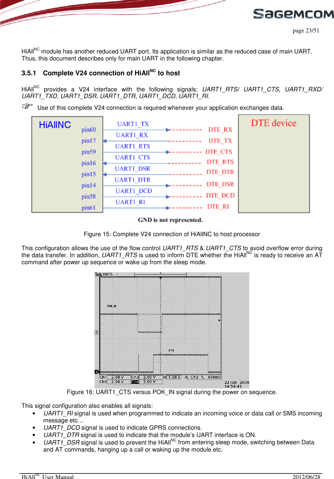
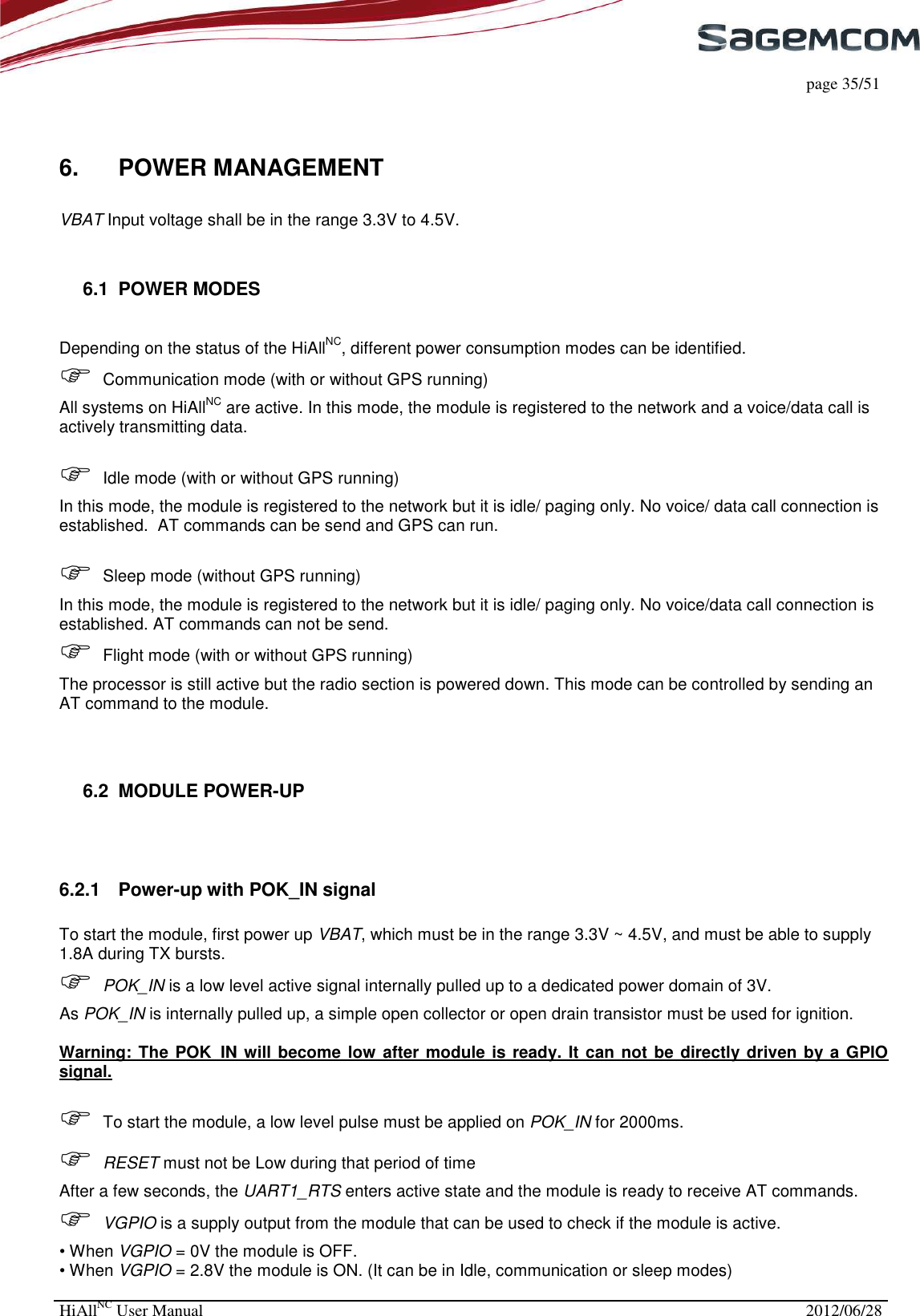
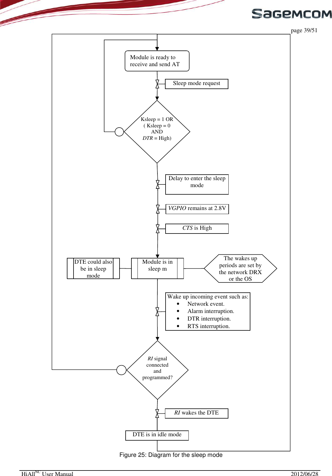
![Page 5/51 HiAllNC User Manual 2012/06/28 1 OVERVIEW 1.1 OBJECT OF THE DOCUMENT The aim of this document is to provide technical guidelines to help the customer to design solutions based on HiAllNC module. 1.2 REFERENCE DOCUMENTS [1] URD1 5717.1 004 72589 - HiAllNC Technical Specification [2] URD1 5635.1 008 70248 - AT Command Set for SAGEMCOM Modules [3] URD1 5635.1 118 72618 – Radio Application Note for Hilo Modules [4] URD1 5696 3 001 72497 - HiLoNC-3GPS Technical Specification 1.3 DOCUMENT MODIFICATIONS The information presented in this document should be accurate and reliable. However Sagemcom assumes no responsibility for its use, nor any infringement of patents or other third party rights which may result from its use. This document is subject to change without notice. 1.4 CONVENTIONS SIGNAL NAME: All signal names written on the pins of the HiAllNC module are in italics. Specific attention must be granted to the information given here. 1.5 TERMS AND ABBREVIATION ADC Analog to Digital Converter CODEC Coder-Decoder CLIP Calling Line Identification Presentation COLP Connected Line Identification Presentation CLIR Calling Line Identification Restriction COLR Connected Line Identification Restriction CTS Clear To Send CSD Circuit Switched Data CS Codec Scheme DCS Digital Communications System DSR Data Set Ready DTR Data Terminal Ready EDGE Enhanced Data Rate for GSM Evolution EGSM Extended GSM ENS Enhanced network selection EONS Enhanced operator name string ESD Electrostatic Discharge ETS European Telecommunication Standard FTA Full Type Approval GLONASS GLObal NAvigation Satellite System GNSS Global aeronautical Navigation Satellite System GSM Global System for Mobile communication GPRS General Packet Radio Services GPS Global Positioning System](https://usermanual.wiki/SAGEMCOM-BROANDS/HIALLNC/User-Guide-1749079-Page-5.png)
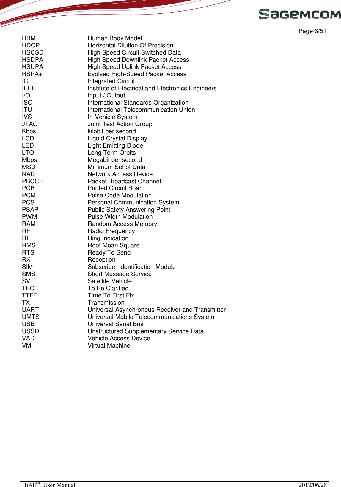
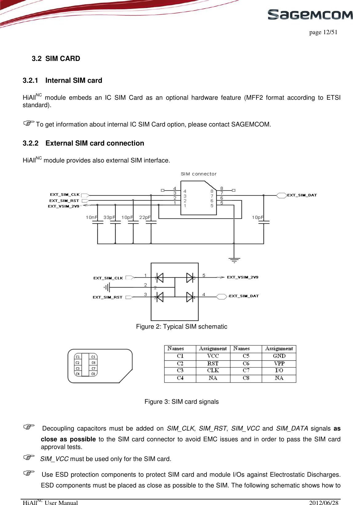
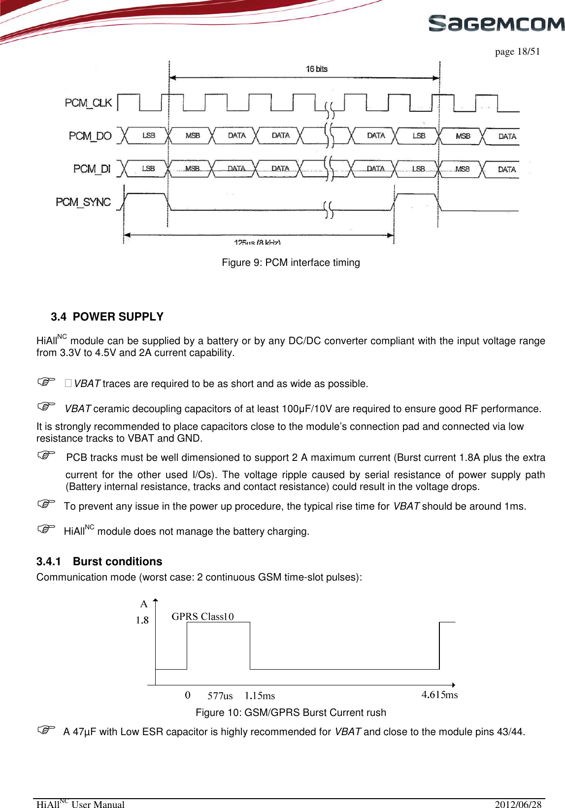
![page 13/51 HiAllNC User Manual 2012/06/28 protect SIM access of the 6 pin connector. This must be performed every time when the SIM card holder is accessed by the end user. If it is necessary to use long SIM bus lines of over 100mm, it is recommended to adopt serial resistors to avoid electrical overshoot on SIM bus signals. Use 56 Ω for the clock line and 10Ω for the reset and data lines. To use external SIM detection function, a GPIO pad must be connected to SIM holder. Figure 4: SIM schematic with protection serial resistors & EXT_SIM_DET signal The schematic above includes a hardware SIM card presence detector. When SIM card is not inserted into SIM holder, Pin9 and Pin10 of SIM holder are disconnected. A GPIO detects a high level during boot. Then there is no initialization to SIM card. When SIM card is inserted, Pin9 is short to Pin10 by mechanic contact, and a GPIO detects a low level during boot. A 22pF capacitor is recommended on EXT_SIM_DET. SIM card must not be removed from its holder while it is still powered. Switch the module off properly with the AT command, then remove the SIM card from its holder. 3.2.3 SIM CARD priority The SIM card selection is performed thanks to KSIMSEL parameter. HiAllNC shall be configured to support to one of the following configuration: - KSIMSEL=0 external SIM only - KSIMSEL=1 internal SIM only - KSIMSEL=2 priority to external SIM if both SIM cards are presents Change of KSIMSEL value is taken into account only after reboot Use of EXT_SIM_DET is mandatory to support KSIMSEL=2 feature (see KSIMSEL description in reference [2])](https://usermanual.wiki/SAGEMCOM-BROANDS/HIALLNC/User-Guide-1749079-Page-13.png)
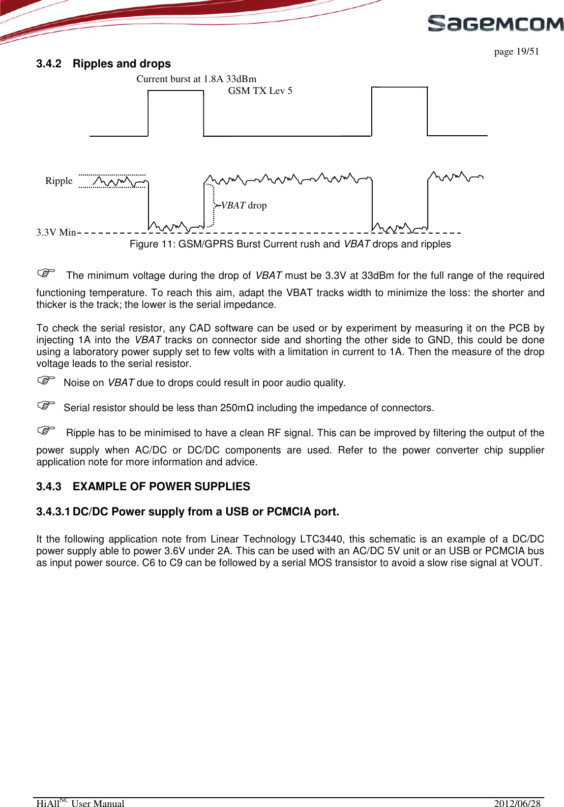
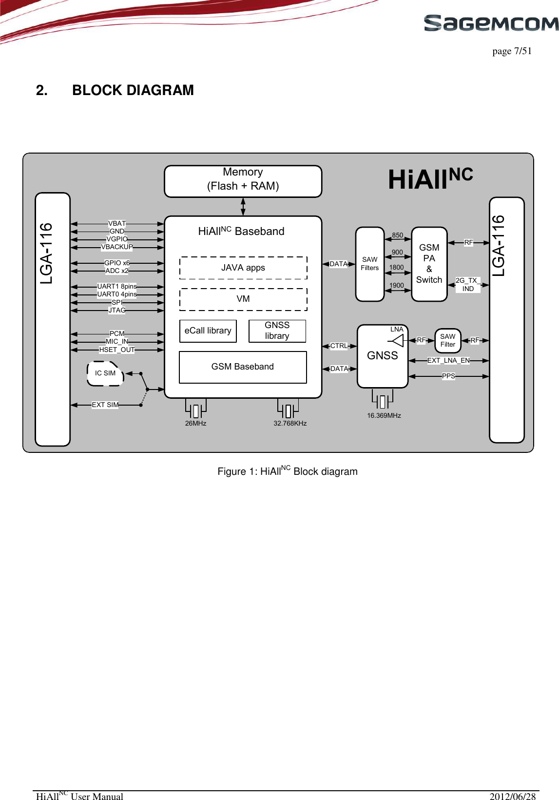
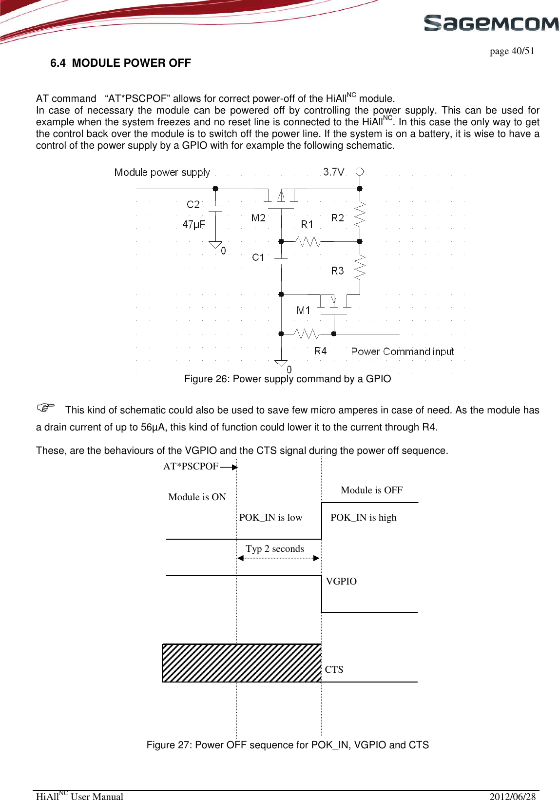
![page 20/51 HiAllNC User Manual 2012/06/28 Figure 12: DC/DC power supply schematic example 3.4.3.2 Simple high current low dropout voltage regulator If the whole power consumption is not an issue, this example of a simple voltage regulator preceded by an AC/DC to 5V converter, can be used to power the module. Figure 13: Example of power supply based on regulator MIC29302WU 3.4.3.3 Simple 4V boost converter The input can be preceded by an AC/DC converter to get the 5V. PGOOD signal can be checked before the ignition of the module. The voltage output is given by: VOUT = 1.24V × [1 + (R1 / R2)] To have 3.7V out R1=100K & R2=49.9K)](https://usermanual.wiki/SAGEMCOM-BROANDS/HIALLNC/User-Guide-1749079-Page-20.png)
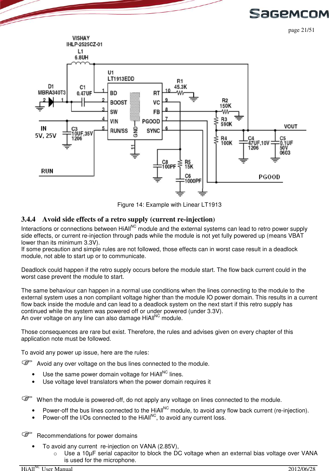
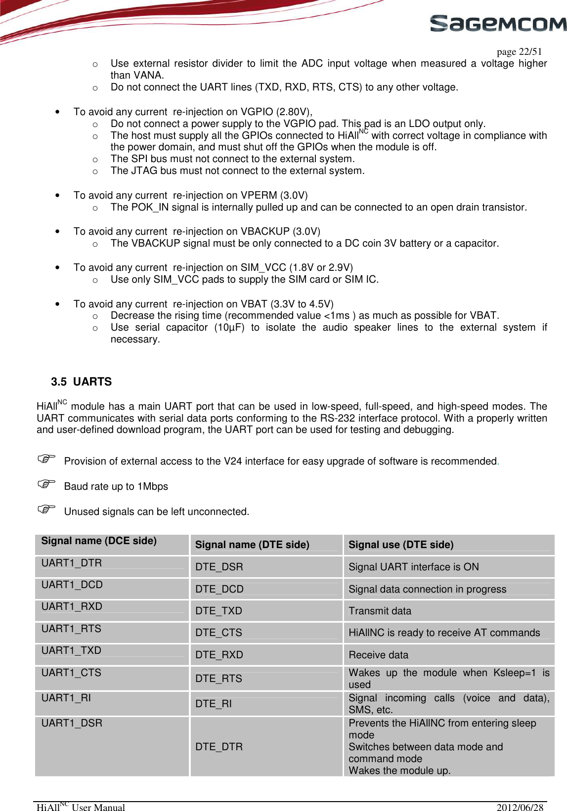
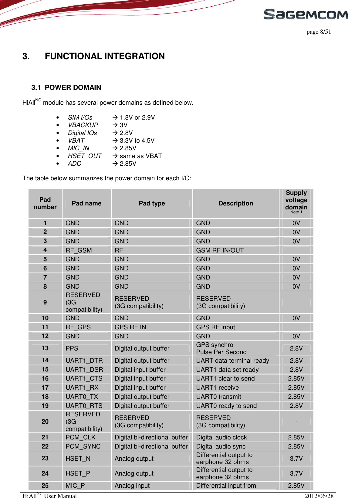
![page 43/51 HiAllNC User Manual 2012/06/28 8. RADIO INTEGRATION Radio engineering skills are mandatory to get accurate radio performance on customer’s product 8.1 GSM antenna connection RF lines shall match 50 ohms impedance In order to achieve optimum sensitivity and output power in radiated mode, it is strongly recommended to implement a matching circuit, as shown on schematic below Figure 28: GSM antenna connection schematic More information about GSM radio design can be found in [3]. 8.2 GNSS antenna connection 8.2.1 Reference schematics HiAllNC module supports both passive and active antenna. HiAllNC embeds a high performance SAW filter. No external filtering is required. Typical schematic for passive antenna is similar to GSM antenna schematic above. If active antenna use, HiAllNC module can be configure to output a GPS_LNA_EN signal, allowing disabling the external LDO when GNSS receiver is in stand-by or shut-down mode. Enabling GPS_LNA_EN is performed through AT+GNSSRUN command If active antenna connection, a power supply shall be connected to the GNSS feed point, according to schematic example below:](https://usermanual.wiki/SAGEMCOM-BROANDS/HIALLNC/User-Guide-1749079-Page-43.png)
![page 44/51 HiAllNC User Manual 2012/06/28 Figure 29: GNSS active antenna connection schematic 8.2.2 Antenna detection For passive antenna, the command AT+KGNSSAD can be used to perform antenna detection. For active antenna, a GPIO can be used to detect the antenna power consumption. The customer needs to fit the current sense circuitry on its own board and match the detection level to the VGPIO level. 8.3 RADIO LAYOUT DESIGN Radio layout guidelines are defined in document [3]](https://usermanual.wiki/SAGEMCOM-BROANDS/HIALLNC/User-Guide-1749079-Page-44.png)