SAGEMCOM BROANDS HIALLNC GSM/GPRS/GNSS Module User Manual HiAllNC
SAGEMCOM SAS GSM/GPRS/GNSS Module HiAllNC
User Manual

Page 1/51
HiAll
NC
User Manual 2012/06/28
HiAllNC User Manual

Page 2/51
HiAll
NC
User Manual 2012/06/28
SOMMAIRE / CONTENTS
1
OVERVIEW...................................................................................................................................................................5
1.1
OBJECT OF THE DOCUMENT.........................................................................................................................5
1.2
REFERENCE DOCUMENTS.............................................................................................................................5
1.3
DOCUMENT MODIFICATIONS ........................................................................................................................5
1.4
CONVENTIONS...................................................................................................................................................5
1.5
TERMS AND ABBREVIATION ..........................................................................................................................5
2.
BLOCK DIAGRAM.......................................................................................................................................................7
3.
FUNCTIONAL INTEGRATION...................................................................................................................................8
3.1
POWER DOMAIN................................................................................................................................................8
3.2
SIM CARD...........................................................................................................................................................12
3.2.1
Internal SIM card........................................................................................................................................12
3.2.2
External SIM card connection ..................................................................................................................12
3.2.3
SIM CARD priority......................................................................................................................................13
3.3
AUDIOS...............................................................................................................................................................14
3.3.1
Analogue audio connection ......................................................................................................................14
3.3.1.1
Connecting microphone and speaker........................................................................................................14
3.3.1.1.1
Notes for microphone ...........................................................................................................................14
3.3.1.1.2
Notes for speaker ..................................................................................................................................15
3.3.1.2
Recommended characteristics for the microphone and speaker ...............................................................16
3.3.1.2.1
Recommended characteristics for the microphone ...............................................................................16
3.3.1.2.2
Recommended characteristics for the speaker......................................................................................16
3.3.1.3
DTMF OVER GSM network....................................................................................................................17
3.3.2
Digital PCM Audio......................................................................................................................................17
3.4
POWER SUPPLY ..............................................................................................................................................18
3.4.1
Burst conditions..........................................................................................................................................18
3.4.2
Ripples and drops ......................................................................................................................................19
3.4.3
EXAMPLE OF POWER SUPPLIES ........................................................................................................19
3.4.3.1
DC/DC Power supply from a USB or PCMCIA port..........................................................................19
3.4.3.2
Simple high current low dropout voltage regulator............................................................................20
3.4.3.3
Simple 4V boost converter....................................................................................................................20
3.4.4
Avoid side effects of a retro supply (current re-injection)............................................................................21
3.5
UARTS.................................................................................................................................................................22
3.5.1
Complete V24 connection of HiAll
NC
to host ..........................................................................................23
3.5.2
Complete V24 interface with PC..............................................................................................................24
3.5.3
Partial V24 (RX-TX-RTS-CTS) connection of HiAllNC to host............................................................25
3.5.4
Partial V24 (RX-TX) – connection HiAll
NC
- host ...................................................................................26
3.6
SPI ........................................................................................................................................................................27
3.7
GPIOS .................................................................................................................................................................27
3.8
ADCS...................................................................................................................................................................28
3.9
BACKUP BATTERY ..........................................................................................................................................28
3.9.1
Backup battery function features .............................................................................................................28
3.9.2
Current consumption on the backup battery..........................................................................................28
3.9.3
Internal HiAll
NC
charging function.............................................................................................................28
3.9.4
Capacitor backup battery technology......................................................................................................29
4.
UNUSED PINS POLICY.............................................................................................................................................30
5.
SCALABILITY WITH HILO
NC
-3GPS........................................................................................................................32
6.
POWER MANAGEMENT ..........................................................................................................................................35
6.1
POWER MODES ...............................................................................................................................................35
6.2
MODULE POWER-UP ......................................................................................................................................35
6.2.1
Power-up with POK_IN signal..................................................................................................................35
6.2.2
IO DC Presence before Power on...........................................................................................................36
6.2.3
MODULE RESET.......................................................................................................................................36
6.3
POWER ON AND SLEEP DIAGRAMS ..........................................................................................................37
6.4
MODULE POWER OFF....................................................................................................................................40
6.5
MODULE SLEEP MODE ..................................................................................................................................41
7.
ESD & EMC RECOMMENDATIONS .......................................................................................................................42
7.1
HiAll
NC
MODULE ................................................................................................................................................42

Page 3/51
HiAll
NC
User Manual 2012/06/28
7.2
Module handling.................................................................................................................................................42
7.3
Customer’s product with HiAll
NC
......................................................................................................................42
7.4
Analysis ...............................................................................................................................................................42
7.5
Recommendations to avoid ESD issues ........................................................................................................42
8.
RADIO INTEGRATION..............................................................................................................................................43
8.1
GSM antenna connection......................................................................................................................................43
8.2
GNSS antenna connection...................................................................................................................................43
8.2.1
Reference schematics...............................................................................................................................43
8.2.2
Antenna detection ......................................................................................................................................44
8.3
RADIO LAYOUT DESIGN ................................................................................................................................44
9.
AUDIO INTEGRATION .............................................................................................................................................45
9.1
MECHANICAL INTEGRATION AND ACOUSTICS ......................................................................................45
9.2
ELECTRONICS AND LAYOUT .......................................................................................................................45
10.
LAYOUT RECOMMENDATIONS ON CUSTOMER BOARD ............................................................................47
10.1
GENERAL RECOMMENDATIONS ON LAYOUT.....................................................................................47
10.1.1
Ground.........................................................................................................................................................47
10.1.2
Power supplies ...........................................................................................................................................47
10.1.3
Clocks ..........................................................................................................................................................48
10.1.4
Data bus and other signals.......................................................................................................................48
10.1.5
Radio............................................................................................................................................................48
10.1.6
Audio............................................................................................................................................................48
10.2
EXAMPLE OF LAYOUT FOR CUSTOMER’S BOARD............................................................................49
11.
LABEL .....................................................................................................................................................................49
12.
FCC LEGAL INFORMATION................................................................................................................................49
12.1
FCC REGULATIONS ....................................................................................................................................49
12.2
RF EXPOSURE INFORMATION.................................................................................................................50
12.3
IC REGULATIONS.........................................................................................................................................50

Page 4/51
HiAll
NC
User Manual 2012/06/28
FIGURES LIST
Figure 1: HiAll
NC
Block diagram .............................................................................................................................................7
Figure 2: Typical SIM schematic ...........................................................................................................................................12
Figure 3: SIM card signals......................................................................................................................................................12
Figure 4: SIM schematic with protection serial resistors & EXT_SIM_DET signal..............................................................13
Figure 5: Analogue audio connection.....................................................................................................................................14
Figure 6: Filter and ESD protection of microphone ...............................................................................................................15
Figure 7: Filter and ESD protection of 32 ohms speaker........................................................................................................15
Figure 8: Example of D class TPA2010D1 1Watt audio amplifier connections ....................................................................16
Figure 9: PCM interface timing..............................................................................................................................................18
Figure 10: GSM/GPRS Burst Current rush ............................................................................................................................18
Figure 11: GSM/GPRS Burst Current rush and VBAT drops and ripples...............................................................................19
Figure 12: DC/DC power supply schematic example.............................................................................................................20
Figure 13: Example of power supply based on regulator MIC29302WU ..............................................................................20
Figure 14: Example with Linear LT1913 ...............................................................................................................................21
Figure 15: Complete V24 connection of HiAllNC to host processor.....................................................................................23
Figure 16: UART1_CTS versus POK_IN signal during the power on sequence. ..................................................................23
Figure 17: Connection to a data cable ....................................................................................................................................24
Figure 18: Example of a connection to a data cable with a MAX3238E................................................................................25
Figure 19: Partial V24 connection (4 wires) of HiAll
NC
to host processor.............................................................................25
Figure 20: Partial V24 connection (2 wires) of HiAll
NC
to host processor.............................................................................26
Figure 21: SPI HE10 pin – TOP VIEW..................................................................................................................................27
Figure 22: internal charging of backup battery or 10uF capacitor..........................................................................................29
Figure 23: Reset command of the HiAll
NC
by an external GPIO............................................................................................36
Figure 24: Diagram for the power on .....................................................................................................................................38
Figure 25: Diagram for the sleep mode ..................................................................................................................................39
Figure 26: Power supply command by a GPIO ......................................................................................................................40
Figure 27: Power OFF sequence for POK_IN, VGPIO and CTS...........................................................................................40
Figure 28: GSM antenna connection schematic .....................................................................................................................43
Figure 29: GNSS active antenna connection schematic .........................................................................................................44
Figure 30: Layout of audio differential signals on a layer n...................................................................................................48
Figure 31: Adjacent layers of audio differential signals.........................................................................................................48
Figure 32: 6 layers PCB stack-up ...........................................................................................................................................49

Page 5/51
HiAll
NC
User Manual 2012/06/28
1 OVERVIEW
1.1 OBJECT OF THE DOCUMENT
The aim of this document is to provide technical guidelines to help the customer to design solutions based on
HiAll
NC
module.
1.2 REFERENCE DOCUMENTS
[1] URD1 5717.1 004 72589 - HiAll
NC
Technical Specification
[2] URD1 5635.1 008 70248 - AT Command Set for SAGEMCOM Modules
[3] URD1 5635.1 118 72618 – Radio Application Note for Hilo Modules
[4] URD1 5696 3 001 72497 - HiLo
NC
-3GPS Technical Specification
1.3 DOCUMENT MODIFICATIONS
The information presented in this document should be accurate and reliable. However Sagemcom assumes no
responsibility for its use, nor any infringement of patents or other third party rights which may result from its use.
This document is subject to change without notice.
1.4 CONVENTIONS
SIGNAL NAME: All signal names written on the pins of the HiAll
NC
module are in italics.
Specific attention must be granted to the information given here.
1.5 TERMS AND ABBREVIATION
ADC Analog to Digital Converter
CODEC Coder-Decoder
CLIP Calling Line Identification Presentation
COLP Connected Line Identification Presentation
CLIR Calling Line Identification Restriction
COLR Connected Line Identification Restriction
CTS Clear To Send
CSD Circuit Switched Data
CS Codec Scheme
DCS Digital Communications System
DSR Data Set Ready
DTR Data Terminal Ready
EDGE Enhanced Data Rate for GSM Evolution
EGSM Extended GSM
ENS Enhanced network selection
EONS Enhanced operator name string
ESD Electrostatic Discharge
ETS European Telecommunication Standard
FTA Full Type Approval
GLONASS GLObal NAvigation Satellite System
GNSS Global aeronautical Navigation Satellite System
GSM Global System for Mobile communication
GPRS General Packet Radio Services
GPS Global Positioning System

Page 6/51
HiAll
NC
User Manual 2012/06/28
HBM Human Body Model
HDOP Horizontal Dilution Of Precision
HSCSD High Speed Circuit Switched Data
HSDPA High Speed Downlink Packet Access
HSUPA High Speed Uplink Packet Access
HSPA+ Evolved High-Speed Packet Access
IC Integrated Circuit
IEEE Institute of Electrical and Electronics Engineers
I/O Input / Output
ISO International Standards Organization
ITU International Telecommunication Union
IVS In-Vehicle System
JTAG Joint Test Action Group
Kbps kilobit per second
LCD Liquid Crystal Display
LED Light Emitting Diode
LTO Long Term Orbits
Mbps Megabit per second
MSD Minimum Set of Data
NAD Network Access Device
PBCCH Packet Broadcast Channel
PCB Printed Circuit Board
PCM Pulse Code Modulation
PCS Personal Communication System
PSAP Public Safety Answering Point
PWM Pulse Width Modulation
RAM Random Access Memory
RF Radio Frequency
RI Ring Indication
RMS Root Mean Square
RTS Ready To Send
RX Reception
SIM Subscriber Identification Module
SMS Short Message Service
SV Satellite Vehicle
TBC To Be Clarified
TTFF Time To First Fix
TX Transmission
UART Universal Asynchronous Receiver and Transmitter
UMTS Universal Mobile Telecommunications System
USB Universal Serial Bus
USSD Unstructured Supplementary Service Data
VAD Vehicle Access Device
VM Virtual Machine
page 7/51
HiAll
NC
User Manual 2012/06/28
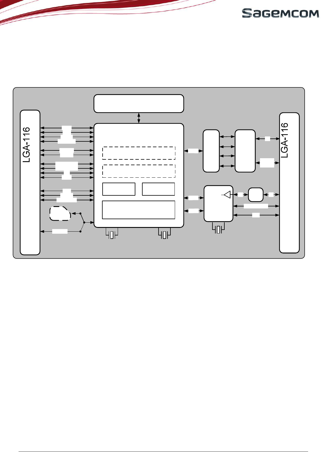
2. BLOCK DIAGRAM
850
HiAllNC
GSM Baseband
eCall library GNSS
library
VM
JAVA apps
Memory
(Flash + RAM)
GNSS
SAW
Filters
GSM
PA
&
Switch
900
1800
1900
DATA
CTRL
DATA
16.369MHz
26MHz 32.768KHz
IC SIM
EXT SIM
UART1 8pins
UART0 4pins
VBAT
GND
VGPIO
VBACKUP
GPIO x6
ADC x2
SPI
MIC_IN
HSET_OUT
PCM
RF
RF
JTAG
HiAllNC Baseband
EXT_LNA_EN
PPS
2G_TX_
IND
SAW
Filter
RF
LNA
Figure 1: HiAll
NC
Block diagram
page 8/51
HiAll
NC
User Manual 2012/06/28
3. FUNCTIONAL INTEGRATION
3.1 POWER DOMAIN
HiAll
NC
module has several power domains as defined below.
• SIM I/Os 1.8V or 2.9V
• VBACKUP 3V
• Digital IOs 2.8V
• VBAT 3.3V to 4.5V
• MIC_IN 2.85V
• HSET_OUT same as VBAT
• ADC 2.85V
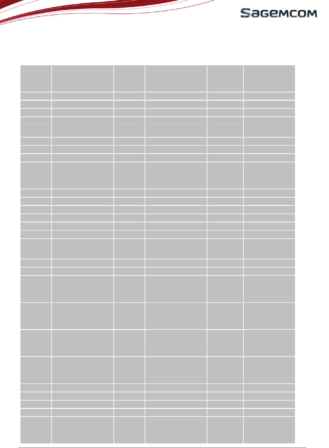
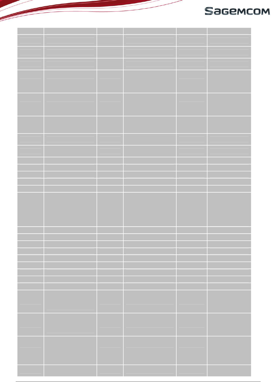
The table below summarizes the power domain for each I/O:
Pad
number Pad name Pad type Description
Supply
voltage
domain
Note 1
1 GND GND GND 0V
2 GND GND GND 0V
3 GND GND GND 0V
4 RF_GSM RF GSM RF IN/OUT
5 GND GND GND 0V
6 GND GND GND 0V
7 GND GND GND 0V
8 GND GND GND 0V
9 RESERVED
(3G
compatibility)
RESERVED
(3G compatibility) RESERVED
(3G compatibility)
10 GND GND GND 0V
11 RF_GPS GPS RF IN GPS RF input
12 GND GND GND 0V
13 PPS Digital output buffer GPS synchro
Pulse Per Second 2.8V
14 UART1_DTR Digital output buffer UART data terminal ready 2.8V
15 UART1_DSR Digital input buffer UART1 data set ready 2.8V
16 UART1_CTS Digital input buffer UART1 clear to send 2.85V
17 UART1_RX Digital input buffer UART1 receive 2.85V
18 UART0_TX Digital output buffer UART0 transmit 2.85V
19 UART0_RTS Digital output buffer UART0 ready to send 2.8V
20 RESERVED
(3G
compatibility)
RESERVED
(3G compatibility) RESERVED
(3G compatibility) -
21 PCM_CLK Digital bi-directional buffer Digital audio clock 2.85V
22 PCM_SYNC Digital bi-directional buffer Digital audio sync 2.85V
23 HSET_N Analog output Differential output to
earphone 32 ohms 3.7V
24 HSET_P Analog output Differential output to
earphone 32 ohms 3.7V
25 MIC_P Analog input Differential input from 2.85V
page 9/51
HiAll
NC
User Manual 2012/06/28
microphone
26 MIC_N Analog input Differential input from
microphone 2.85V
27 RESET Digital input Module Reset 2.8V
28 VBACKUP Power supply input/output Backup battery power
supply 3V
29 VBAT Power supply input +3.7V power supply
(nominal) 3.7V
30 ADC1 Analog input Analog input to digital
converter 2.85V
31 ADC0 Analog input Analog input to digital
converter 2.85V
32 POK_IN Digital input Module power on signal 3V
33 SIM_VCC Power supply output SIM power supply 1.8V/2.9V
34 SIM_DATA Digital bi-directional buffer SIM data 1.8V/2.9V
35 SIM_CLK Digital output buffer SIM clock 1.8V/2.9V
36 GPIO1 Digital bi-directional buffer
General purpose
input/output 1 2.8V
37 SPI_IRQ Digital input buffer Serial peripheral interface.
To be connected for debug
purpose. 2.8V
38 RESERVED
(futur use) RESERVED
(futur use) RESERVED
(futur use)
39 GPS_EXT_LN
A_EN Digital output buffer GPS LNA Enable 2.8V
40 GPIO2 Digital bi-directional buffer General purpose
input/output 2 2.8V
41 GPIO3 Digital bi-directional buffer General purpose
input/output 3 2.8V
42 TRST Digital bi-directional buffer JTAG reset 2.8V
43 VBAT_PA Power supply input for PA +3.7V power supply
(nominal) 3.7V
44 VBAT_PA Power supply input for PA +3.7V power supply
(nominal) 3.7V
45 GND GND GND 0V
46 GND GND GND 0V
47 GND GND GND 0V
48 GND GND GND 0V
49 GND GND GND 0V
50 GND GND GND 0V
51 GND GND GND 0V
52 GND GND GND 0V
53 GND GND GND 0V
54 GND GND GND 0V
55 GND GND GND 0V
56 GND GND GND 0V
57 VBAT Power supply input +3.7V power supply
(nominal) 3.7V
58 UART1_DCD Digital output buffer UART data carrier detect 2.8V
59 UART1_RTS Digital output buffer UART1 ready to send 2.85V
60 UART1_TX Digital output buffer UART1 transmit 2.85V
61 UART1_RI Digital output buffer UART1 ring indicator 2.8V
62 UART0_RX Digital input buffer UART0 receive 2.85V
63 UART0_CTS Digital input buffer UART0 clear to send 2.8V
64 RESERVED RESERVED RESERVED -
page 10/51
HiAll
NC
User Manual 2012/06/28
(3G
compatibility) (3G compatibility) (3G compatibility)
65 PCM_OUT Digital output buffer Digital audio out 2.85V
66 PCM_IN Digital input buffer Digital audio in 2.85V
67 RESERVED
(3G
compatibility)
RESERVED
(3G compatibility) RESERVED
(3G compatibility) -
68 RESERVED
(3G
compatibility)
RESERVED
(3G compatibility) RESERVED
(3G compatibility) -
69 RESERVED
(3G
compatibility)
RESERVED
(3G compatibility) RESERVED
(3G compatibility) -
70 RESERVED
(3G
compatibility)
RESERVED
(3G compatibility) RESERVED
(3G compatibility) -
71 VGPIO Power supply Power supply for external
components 2.8V
72 SPI_IN Digital input buffer Serial peripheral interface.
To be connected for debug
purpose. 2.8V
73 SPI_OUT Digital output buffer Serial peripheral interface.
To be connected for debug
purpose. 2.8V
74 SPI_SEL Digital bi-directional buffer Serial peripheral interface.
To be connected for debug
purpose. 2.8V
75 SPI_CLK Digital bi-directional buffer Serial peripheral interface.
To be connected for debug
purpose. 2.8V
76 TMS Digital input buffer JTAG mode select input 2.8V
77 TDI Digital input buffer JTAG data input 2.8V
78 TDO Digital output buffer JTAG data output 2.8V
79 SIM_RST Digital output buffer SIM reset 1.8V/2.9V
80 JTAG_TEST Digital input buffer JTAG TEST input 2.8V
81 RESERVED
(Factory use) RESERVED
(Factory use) Factory use. Do not
connect.
82 TCK Digital input buffer JTAG clock input 2.8V
83 GPIO4 Digital bi-directional buffer General purpose
input/output 4 2.8V
84 GPIO5 Digital bi-directional buffer General purpose
input/output 5 2.8V
85 GPIO6 Digital bi-directional buffer General purpose
input/output 6 2.8V
86 VIO_SEL Digital input buffer VGPIO voltage selection
87 2G_RF_IND Digital output buffer 2G Transmit indicator 2.85V
88 RTCK Digital output buffer JTAG return clock 2.8V
89 GND GND GND 0V
90 GND GND GND 0V
91 GND GND GND 0V
92 GND GND GND 0V
93 GND GND GND 0V
94 GND GND GND 0V
95 GND GND GND 0V
96 GND GND GND 0V
97 GND GND GND 0V
page 11/51
HiAll
NC
User Manual 2012/06/28
98 GND GND GND 0V
99 GND GND GND 0V
100 GND GND GND 0V
101 GND GND GND 0V
102 GND GND GND 0V
103 GND GND GND 0V
104 GND GND GND 0V
105 GND GND GND 0V
106 GND GND GND 0V
107 GND GND GND 0V
108 GND GND GND 0V
109 GND GND GND 0V
110 GND GND GND 0V
111 GND GND GND 0V
112 GND GND GND 0V
113 GND GND GND 0V
114 GND GND GND 0V
115 GND GND GND 0V
116 GND GND GND 0V
Note 1: VIO_SEL (Pad86) left unconnected
.
Do not power the module I/O with a voltage over the specified limits, this could damage the module.
page 12/51
HiAll
NC
User Manual 2012/06/28
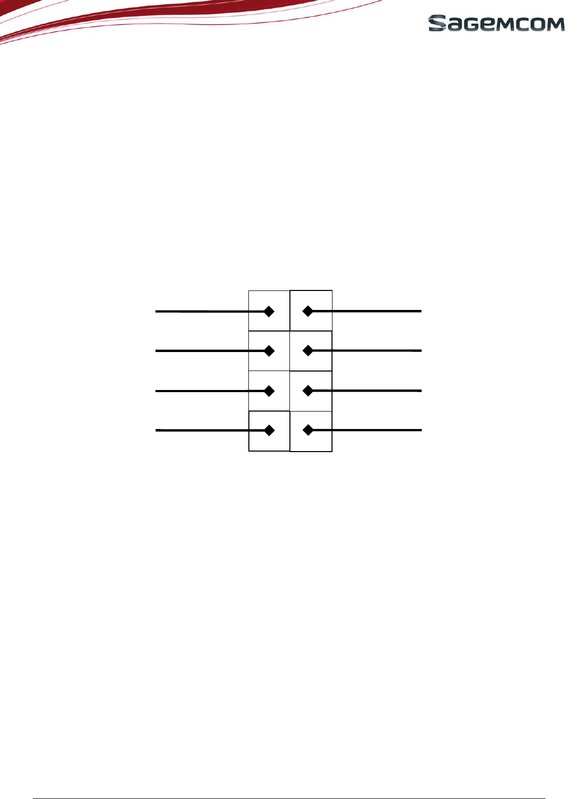
3.2 SIM CARD
3.2.1 Internal SIM card
HiAll
NC
module embeds an IC SIM Card as an optional hardware feature (MFF2 format according to ETSI
standard).
To get information about internal IC SIM Card option, please contact SAGEMCOM.
3.2.2 External SIM card connection
HiAll
NC
module provides also external SIM interface.
Figure 2: Typical SIM schematic
Figure 3: SIM card signals
Decoupling capacitors must be added on SIM_CLK, SIM_RST, SIM_VCC and SIM_DATA signals as
close as possible to the SIM card connector to avoid EMC issues and in order to pass the SIM card
approval tests.
SIM_VCC must be used only for the SIM card.
Use ESD protection components to protect SIM card and module I/Os against Electrostatic Discharges.
ESD components must be placed as close as possible to the SIM. The following schematic shows how to
page 13/51
HiAll
NC
User Manual 2012/06/28
protect SIM access of the 6 pin connector. This must be performed every time when the SIM card holder
is accessed by the end user.
If it is necessary to use long SIM bus lines of over 100mm, it is recommended to adopt serial resistors to
avoid electrical overshoot on SIM bus signals. Use 56 Ω for the clock line and 10Ω for the reset and data
lines.
To use external SIM detection function, a GPIO pad must be connected to SIM holder.
Figure 4: SIM schematic with protection serial resistors & EXT_SIM_DET signal
The schematic above includes a hardware SIM card presence detector. When SIM card is not inserted into SIM
holder, Pin9 and Pin10 of SIM holder are disconnected. A GPIO detects a high level during boot. Then there is
no initialization to SIM card. When SIM card is inserted, Pin9 is short to Pin10 by mechanic contact, and a GPIO
detects a low level during boot.
A
22pF capacitor is recommended on EXT_SIM_DET.
SIM card must not be removed from its holder while it is still powered. Switch the module off properly with
the AT command, then remove the SIM card from its holder.
3.2.3 SIM CARD priority
The SIM card selection is performed thanks to KSIMSEL parameter.
HiAll
NC
shall be configured to support to one of the following configuration:
- KSIMSEL=0 external SIM only
- KSIMSEL=1 internal SIM only
- KSIMSEL=2 priority to external SIM if both SIM cards are presents
Change of KSIMSEL value is taken into account only after reboot
Use of EXT_SIM_DET is mandatory to support KSIMSEL=2 feature (see KSIMSEL description in
reference [2])
page 14/51
HiAll
NC
User Manual 2012/06/28
3.3 AUDIOS
The HiAll
NC
module provides both analogue and digital audio interfaces.
3.3.1 Analogue audio connection
HiAll
NC
module features one input path and one output path for analogue audio. Both the input path and the
output path are differential. The design examples in the following chapter will take into account the EMC, ESD
protections, and reducing the possible TDMA noise in sensitive area by performing the given routing rules.
Note that acoustic engineering competences are mandatory to get accurate audio performance on
customer’s product.
3.3.1.1 Connecting microphone and speaker
HiAll
NC
module can manage an external microphone (MIC_P/MIC_N) in differential mode and an external
speaker (HSET_OUT_P / HSET_OUT_N) in differential mode. Thus, one speaker and one microphone can be
connected to the module. The 1.4V voltage to bias the microphone is implemented in the module.
The speaker connected to the module should be 32 ohms.
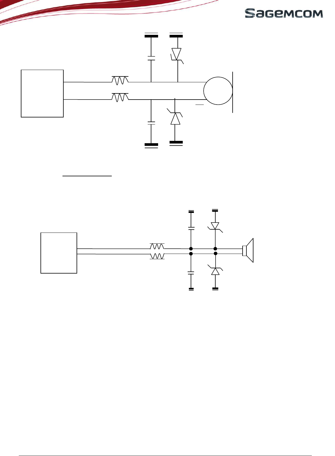
ESD protection
Figure 5: Analogue audio connection
If the design is ESD or EMC sensitive, we strongly recommend reading the notes below.
A poor audio quality could either come from the PCB routing and placement or from the chosen components (or
even both).
3.3.1.1.1 Notes for microphone
Pay attention to the microphone device, it must not be sensitive to RF disturbances.
As described in the layout chapter, differential pairs must be routed in parallel and same length (MIC_P
and MIC_N signals)
If you need to have deported microphone out of the board with long wires, you should pay attention to the
EMC and ESD effect. In those cases, add the following protections to improve your design.
To ensure proper operation of such sensitive signals, they have to be isolated from the others by
analogue ground on customer’s board layout. (Refer to Layout design chapter)
HiAllNC Speaker
MIC
page 15/51
HiAll
NC
User Manual 2012/06/28
Figure 6: Filter and ESD protection of microphone
3.3.1.1.2 Notes for speaker
As explained for the microphone, if the speaker is deported out of the board or is sensitive to ESD, use the
schematic here to improve the audio.
Figure 7: Filter and ESD protection of 32 ohms speaker
HSET_OUT_P, HSET_OUT_N tracks must be larger than other tracks: 0.1mm.
As described in the layout chapter, differential pairs must be routed in parallel and same length
(HSET_OUT_P and HSET_OUT_N signals)
The impedance of audio chain (filter + speaker) must be lower than 32Ω.
To use an external audio amplifier connected to a loud-speaker, use serial capacitors of 10nF on HiAll
NC
audio outputs to connect the audio amplifier.
MIC
33pF
33pF
Ferrite Bead
Ferrite Bead
+
ESD protection
ESD protection
HiAll
NC
HiAll
NC
HSET_OUT_P
HSET_OUT_N
speaker
Ferrite Bead
Ferrite Bead
18pF
18pF
ESD protection
ESD protection
page 16/51
HiAll
NC
User Manual 2012/06/28
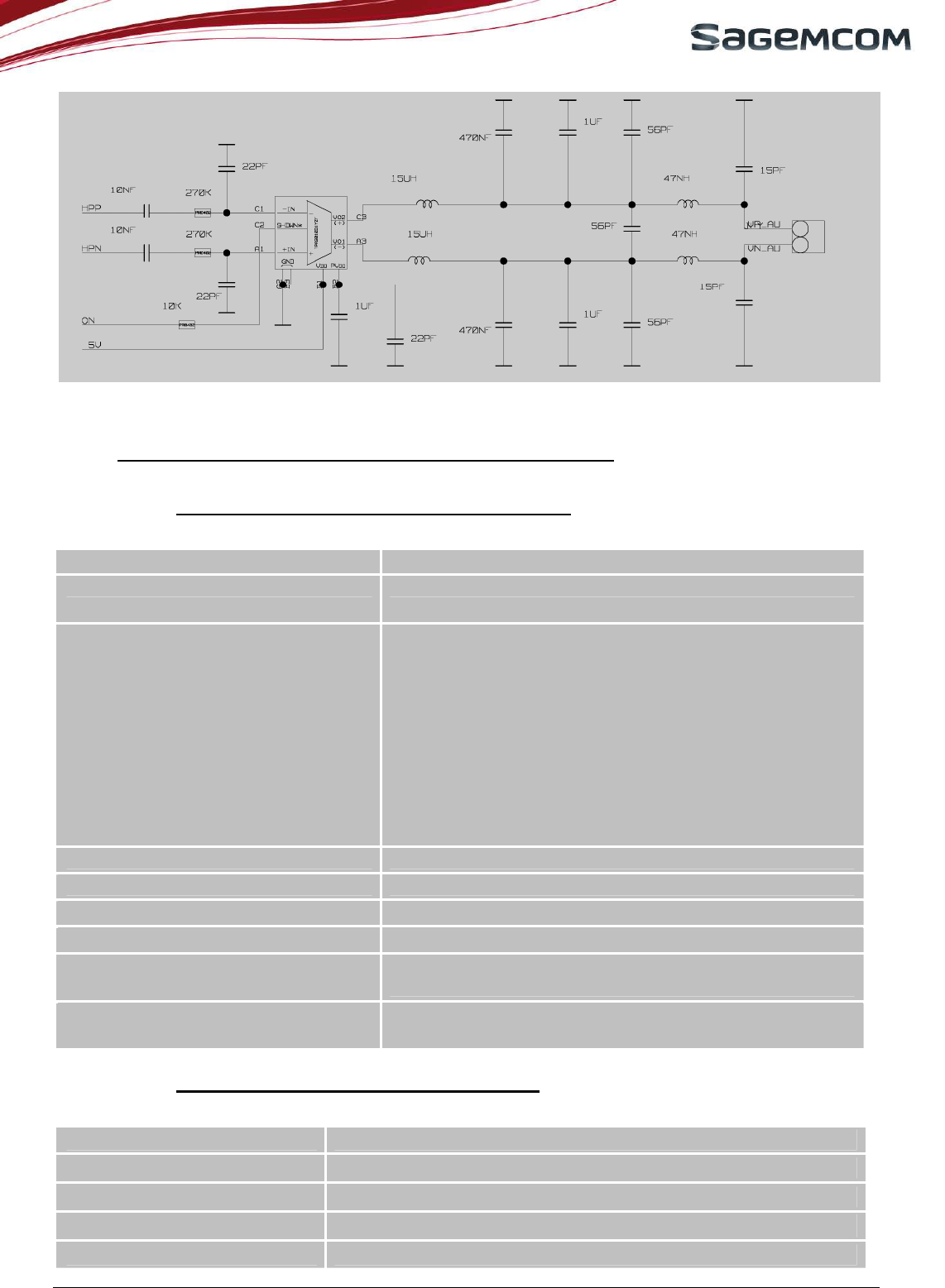
Figure 8: Example of D class TPA2010D1 1Watt audio amplifier connections
3.3.1.2 Recommended characteristics for the microphone and speaker
3.3.1.2.1 Recommended characteristics for the microphone
Item to be inspected Acceptance criterion
Sensitivity - 40 dB SPL +/-3 dB (0 dB = 1 V/Pa @ 1kHz)
Frequency response Limits (relatives values)
Freq. (Hz) Lower limit Upper limit
100 -1 1
200 -1 1
300 -1 1
1000 0 0
2000 -1 1
3000 -1.5 1.5
3400 -2 2
4000 -2 2
Current consumption 1 mA (maximum)
Operating voltage DC 1 to 3 V (minimum)
S / N ratio 55 dB minimum (A-Curve at 1 kHz, 1 Pa)
Directivity Omni-directional
Maximum input sound pressure level 100 dB SPL (1 kHz)
Maximum distortion 1%
Radio frequency protection Over 800 -1200 MHz and 1700 -2000 MHz, S/N ratio 50
dB minimum (signal 1 kHz, 1 Pa)
3.3.1.2.2 Recommended characteristics for the speaker
Item to be inspected Acceptance criterion
Input power: rated / max 0.1W (Rate)
Audio chain impedance 32 ohm +/- 10% at 1V 1KHz
Frequency Range 300 Hz ~ 4.0 KHz
Sensitivity (S.P.L) >105 dB at 1KHz with IEC318 coupler,
page 17/51
HiAll
NC
User Manual 2012/06/28
Distortion 5% max at 1K Hz, nominal input power
3.3.1.3
DTMF OVER GSM network
Former systems used to transmits data through DTMF modulation on RTC telephone lines.
Audio DTMF tones are not guaranteed over GSM network
This is due to the nature of the GSM Voice CODEC - it is specifically designed for the human voice and does
not faithfully transmit DTMF.
When you press the buttons on your GSM handset during a call, this goes in the Signalling channel - it does not
generate in-band DTMF; the actual DTMF tones are generated in the network.
Therefore if your design needs the DTMF functionality, you should know their transmission over the network is
not at all guaranteed (because of voice codec). This could work or fail depending very strongly on the GSM
network provider. SAGEMCOM does not guarantee any success on using this function.
However tests on HiAll
NC
shown this feature can work on some GSM Networks. Successful transmissions and
receptions have been done with 300ms of characters duration and 200mVpp as input level on microphone
input.
If this function is needed, first try with your network and those parameters then (if success) try to tune
them to fit your specification.
3.3.2 Digital PCM Audio
The HiAll
NC
module features a PCM interface. The PCM interface is a high speed full duplex interface that can
be used to send and receive digital audio data to external audio ICs.The HiAll
NC
PCM interface is highly
configurable:
- PCM master or slave mode
- 8bits or 16 bits data word length
- MSB or LSB first
- Rising or falling sampling clock edge
- Configurable PCM bit clock rate up to 1MHz
Signals Module connector pin
number Description
PCM_CLK 21 Clock
PCM_IN 66 Digital audio input
PCM_OUT 65 Digital audio output
PCM_SYNC 22 Audio signal frame synchronization
page 18/51
HiAll
NC
User Manual 2012/06/28
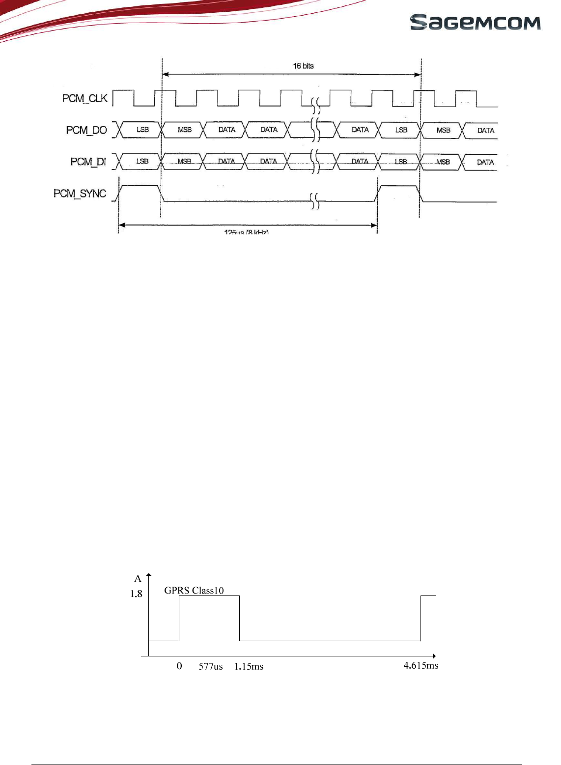
Figure 9: PCM interface timing
3.4 POWER SUPPLY
HiAll
NC
module can be supplied by a battery or by any DC/DC converter compliant with the input voltage range
from 3.3V to 4.5V and 2A current capability.
>
VBAT traces are required to be as short and as wide as possible.
VBAT ceramic decoupling capacitors of at least 100µF/10V are required to ensure good RF performance.
It is strongly recommended to place capacitors close to the module’s connection pad and connected via low
resistance tracks to VBAT and GND.
PCB tracks must be well dimensioned to support 2 A maximum current (Burst current 1.8A plus the extra
current for the other used I/Os). The voltage ripple caused by serial resistance of power supply path
(Battery internal resistance, tracks and contact resistance) could result in the voltage drops.
To prevent any issue in the power up procedure, the typical rise time for VBAT should be around 1ms.
HiAll
NC
module does not manage the battery charging.
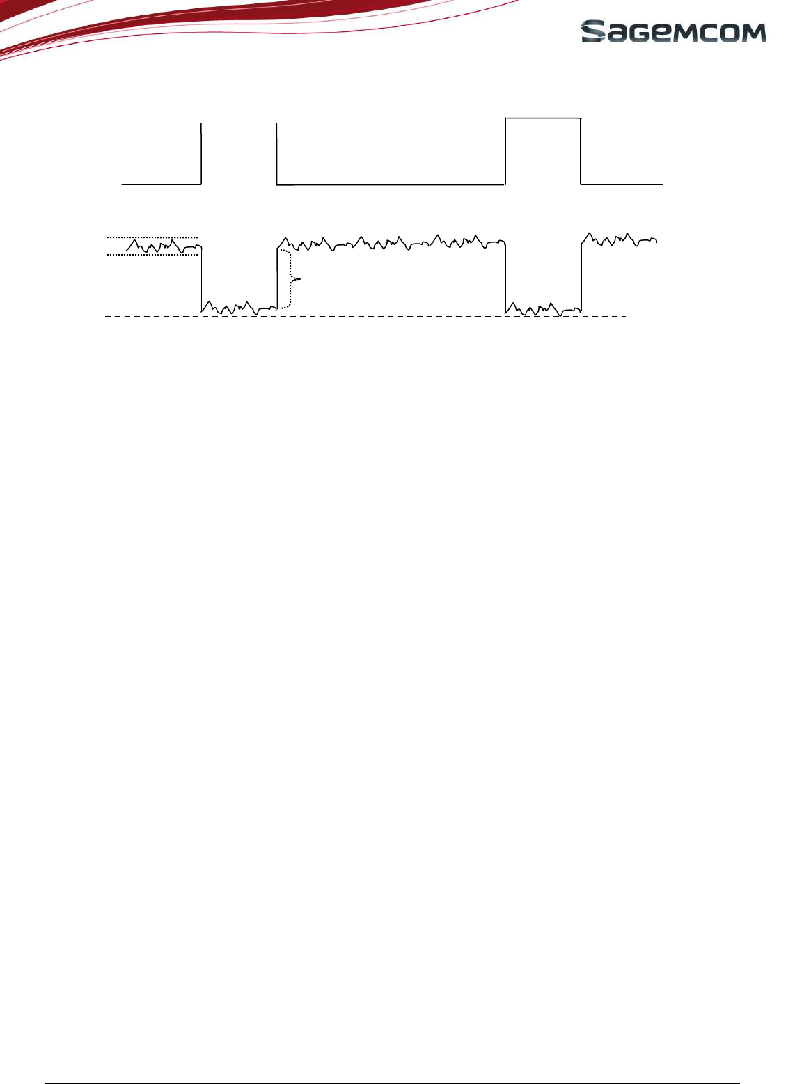
3.4.1 Burst conditions
Communication mode (worst case: 2 continuous GSM time-slot pulses):
Figure 10: GSM/GPRS Burst Current rush
A 47µF with Low ESR capacitor is highly recommended for VBAT and close to the module pins 43/44.
page 19/51
HiAll
NC
User Manual 2012/06/28
3.4.2 Ripples and drops
Figure 11: GSM/GPRS Burst Current rush and VBAT drops and ripples
The minimum voltage during the drop of VBAT must be 3.3V at 33dBm for the full range of the required
functioning temperature. To reach this aim, adapt the VBAT tracks width to minimize the loss: the shorter and
thicker is the track; the lower is the serial impedance.
To check the serial resistor, any CAD software can be used or by experiment by measuring it on the PCB by
injecting 1A into the VBAT tracks on connector side and shorting the other side to GND, this could be done
using a laboratory power supply set to few volts with a limitation in current to 1A. Then the measure of the drop
voltage leads to the serial resistor.
Noise on VBAT due to drops could result in poor audio quality.
Serial resistor should be less than 250mΩ including the impedance of connectors.
Ripple has to be minimised to have a clean RF signal. This can be improved by filtering the output of the
power supply when AC/DC or DC/DC components are used. Refer to the power converter chip supplier
application note for more information and advice.
3.4.3 EXAMPLE OF POWER SUPPLIES
3.4.3.1 DC/DC Power supply from a USB or PCMCIA port.
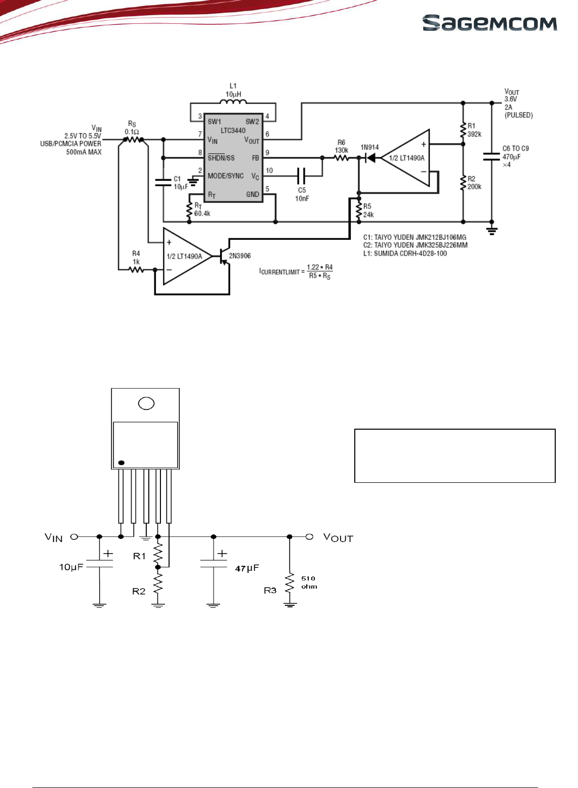
It the following application note from Linear Technology LTC3440, this schematic is an example of a DC/DC
power supply able to power 3.6V under 2A. This can be used with an AC/DC 5V unit or an USB or PCMCIA bus
as input power source. C6 to C9 can be followed by a serial MOS transistor to avoid a slow rise signal at VOUT.
3.3V Min
Ripple
VBAT drop
Current burst at 1.8A 33dBm
GSM TX Lev 5
page 20/51
HiAll
NC
User Manual 2012/06/28
Figure 12: DC/DC power supply schematic example
3.4.3.2 Simple high current low dropout voltage regulator
If the whole power consumption is not an issue, this example of a simple voltage regulator preceded by an
AC/DC to 5V converter, can be used to power the module.
Figure 13: Example of power supply based on regulator MIC29302WU
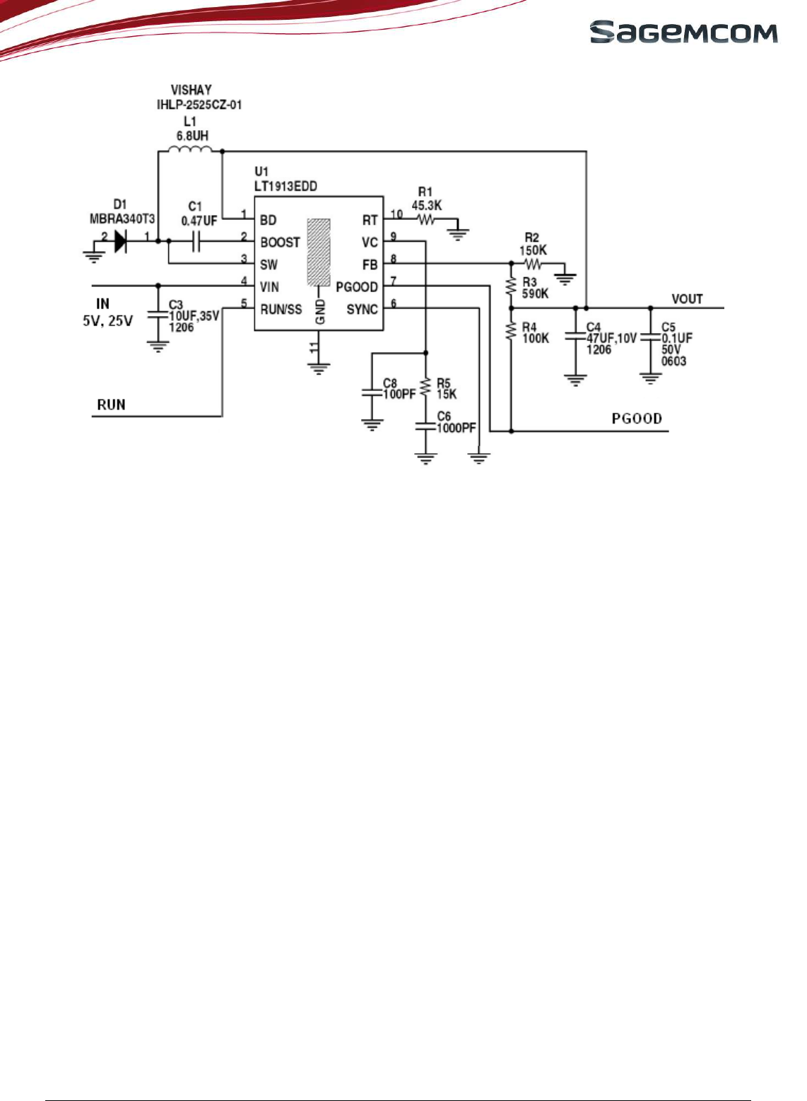
3.4.3.3 Simple 4V boost converter
The input can be preceded by an AC/DC converter to get the 5V. PGOOD signal can be checked before the
ignition of the module.
The voltage output is given by:
VOUT = 1.24V × [1 + (R1 / R2)]
To have 3.7V out R1=100K & R2=49.9K)
page 21/51
HiAll
NC
User Manual 2012/06/28
Figure 14: Example with Linear LT1913
3.4.4 Avoid side effects of a retro supply (current re-injection
)
Interactions or connections between HiAll
NC
module and the external systems can lead to retro power supply
side effects, or current re-injection through pads while the module is not yet fully powered up (means VBAT
lower than its minimum 3.3V).
If some precaution and simple rules are not followed, those effects can in worst case result in a deadlock
module, not able to start up or to communicate.
Deadlock could happen if the retro supply occurs before the module start. The flow back current could in the
worst case prevent the module to start.
The same behaviour can happen in a normal use conditions when the lines connecting to the module to the
external system uses a non compliant voltage higher than the module IO power domain. This results in a current
flow back inside the module and can lead to a deadlock system on the next start if this retro supply has
continued while the system was powered off or under powered (under 3.3V).
An over voltage on any line can also damage HiAll
NC
module.
Those consequences are rare but exist. Therefore, the rules and advises given on every chapter of this
application note must be followed.
To avoid any power up issue, here are the rules:
Avoid any over voltage on the bus lines connected to the module.
• Use the same power domain voltage for HiAll
NC
lines.
• Use voltage level translators when the power domain requires it
When the module is powered-off, do not apply any voltage on lines connected to the module.
• Power-off the bus lines connected to the HiAll
NC
module, to avoid any flow back current (re-injection).
• Power-off the I/Os connected to the HiAll
NC
, to avoid any current loss.
Recommendations for power domains
• To avoid any current re-injection on VANA (2.85V),
o Use a 10µF serial capacitor to block the DC voltage when an external bias voltage over VANA
is used for the microphone.
page 22/51
HiAll
NC
User Manual 2012/06/28
o Use external resistor divider to limit the ADC input voltage when measured a voltage higher
than VANA.
o Do not connect the UART lines (TXD, RXD, RTS, CTS) to any other voltage.
• To avoid any current re-injection on VGPIO (2.80V),
o Do not connect a power supply to the VGPIO pad. This pad is an LDO output only.
o The host must supply all the GPIOs connected to HiAll
NC
with correct voltage in compliance with
the power domain, and must shut off the GPIOs when the module is off.
o The SPI bus must not connect to the external system.
o The JTAG bus must not connect to the external system.
• To avoid any current re-injection on VPERM (3.0V)
o The POK_IN signal is internally pulled up and can be connected to an open drain transistor.
• To avoid any current re-injection on VBACKUP (3.0V)
o The VBACKUP signal must be only connected to a DC coin 3V battery or a capacitor.
• To avoid any current re-injection on SIM_VCC (1.8V or 2.9V)
o Use only SIM_VCC pads to supply the SIM card or SIM IC.
• To avoid any current re-injection on VBAT (3.3V to 4.5V)
o Decrease the rising time (recommended value <1ms ) as much as possible for VBAT.
o Use serial capacitor (10µF) to isolate the audio speaker lines to the external system if
necessary.
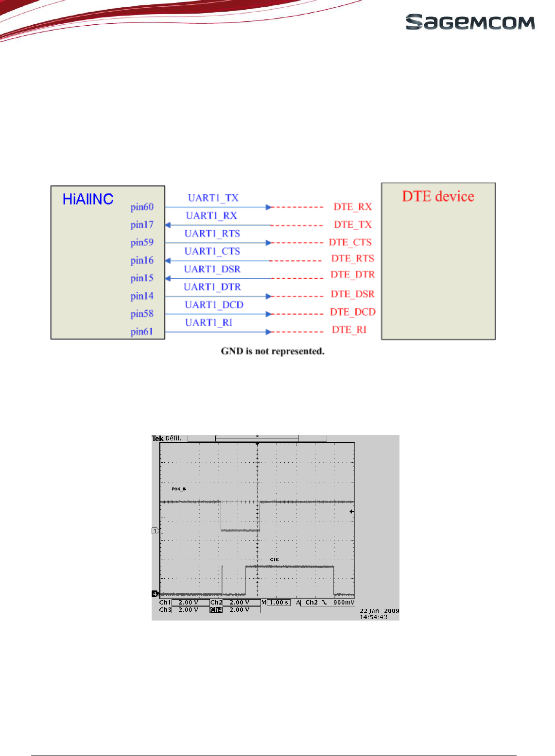
3.5 UARTS
HiAll
NC
module has a main UART port that can be used in low-speed, full-speed, and high-speed modes. The
UART communicates with serial data ports conforming to the RS-232 interface protocol. With a properly written
and user-defined download program, the UART port can be used for testing and debugging.
Provision of external access to the V24 interface for easy upgrade of software is recommended.
Baud rate up to 1Mbps
Unused signals can be left unconnected.
Signal name (DCE side) Signal name (DTE side) Signal use (DTE side)
UART1_DTR DTE_DSR Signal UART interface is ON
UART1_DCD DTE_DCD Signal data connection in progress
UART1_RXD DTE_TXD Transmit data
UART1_RTS DTE_CTS HiAllNC is ready to receive AT commands
UART1_TXD DTE_RXD Receive data
UART1_CTS DTE_RTS Wakes up the module when Ksleep=1 is
used
UART1_RI DTE_RI Signal incoming calls (voice and data),
SMS, etc.
UART1_DSR
DTE_DTR
Prevents the HiAllNC from entering sleep
mode
Switches between data mode and
command mode
Wakes the module up.
page 23/51
HiAll
NC
User Manual 2012/06/28
HiAll
NC
module has another reduced UART port. Its application is similar as the reduced case of main UART.
Thus, this document describes only for main UART in the following chapter.
3.5.1 Complete V24 connection of HiAll
NC
to host
HiAll
NC
provides a V24 interface with the following signals: UART1_RTS/ UART1_CTS, UART1_RXD/
UART1_TXD, UART1_DSR, UART1_DTR, UART1_DCD, UART1_RI.
Use of this complete V24 connection is required whenever your application exchanges data.
Figure 15: Complete V24 connection of HiAllNC to host processor
This configuration allows the use of the flow control UART1_RTS & UART1_CTS to avoid overflow error during
the data transfer. In addition, UART1_RTS is used to inform DTE whether the HiAll
NC
is ready to receive an AT
command after power up sequence or wake up from the sleep mode.
Figure 16: UART1_CTS versus POK_IN signal during the power on sequence.
This signal configuration also enables all signals:
• UART1_RI signal is used when programmed to indicate an incoming voice or data call or SMS incoming
message etc…
• UART1_DCD signal is used to indicate GPRS connections.
• UART1_DTR signal is used to indicate that the module’s UART interface is ON.
• UART1_DSR signal is used to prevent the HiAll
NC
from entering sleep mode, switching between Data
and AT commands, hanging up a call or waking up the module etc.
page 24/51
HiAll
NC
User Manual 2012/06/28
Avoid supplying power to the main UART before the HiAll
NC
is ON, as this may result in power up
sequence error.
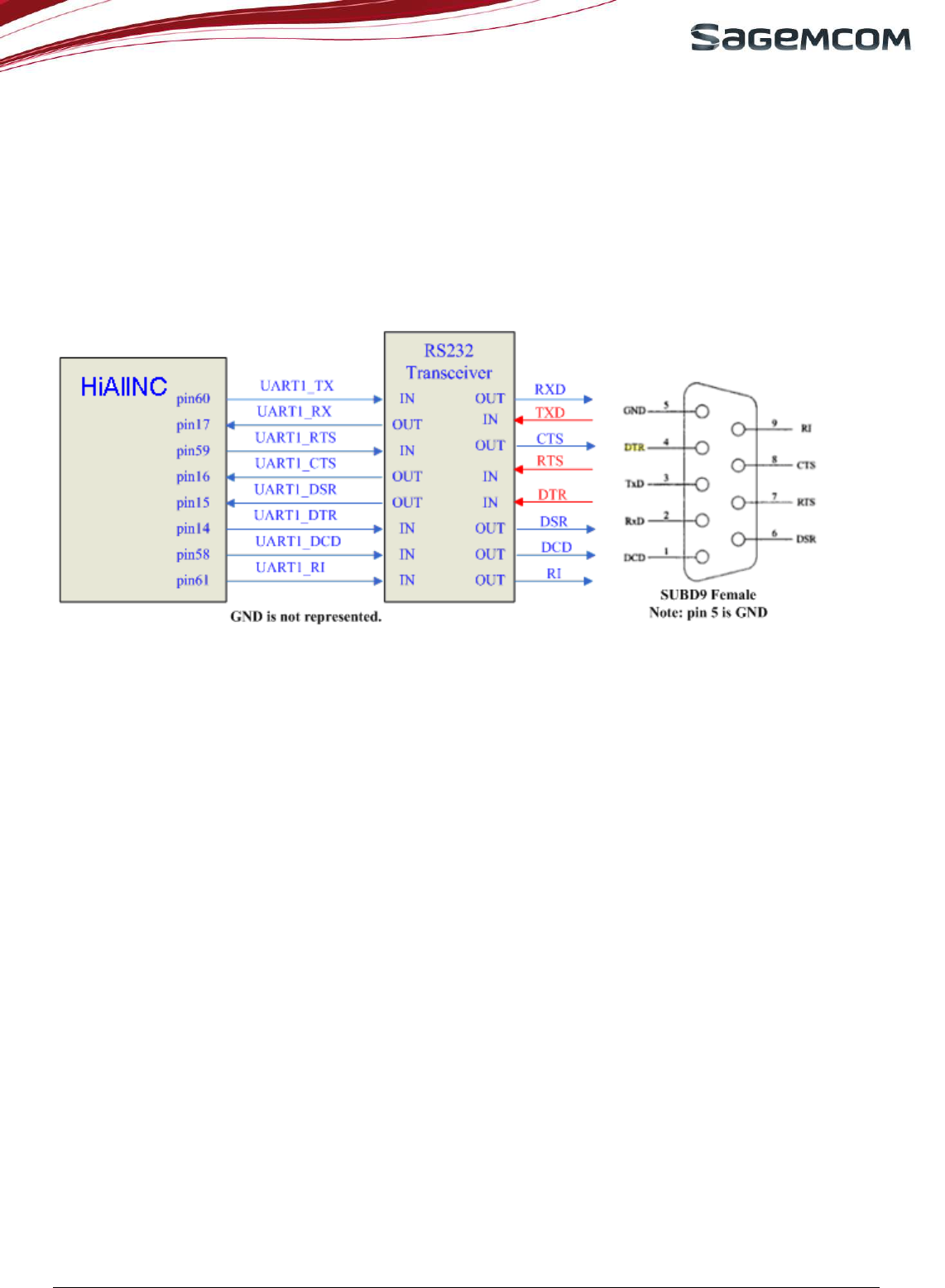
3.5.2 Complete V24 interface with PC
It supports speeds up to 1Mbps (115.2 Kbps with auto bauding).
To use the V24 interface, some level shifter components are necessary, as HiAll
NC
signals need to be converted
to +/- 5V signals compatible with a PC.
Figure 17: Connection to a data cable
Avoid supplying the UART before HiAll
NC
module is ON, as this could result in power up sequence error.
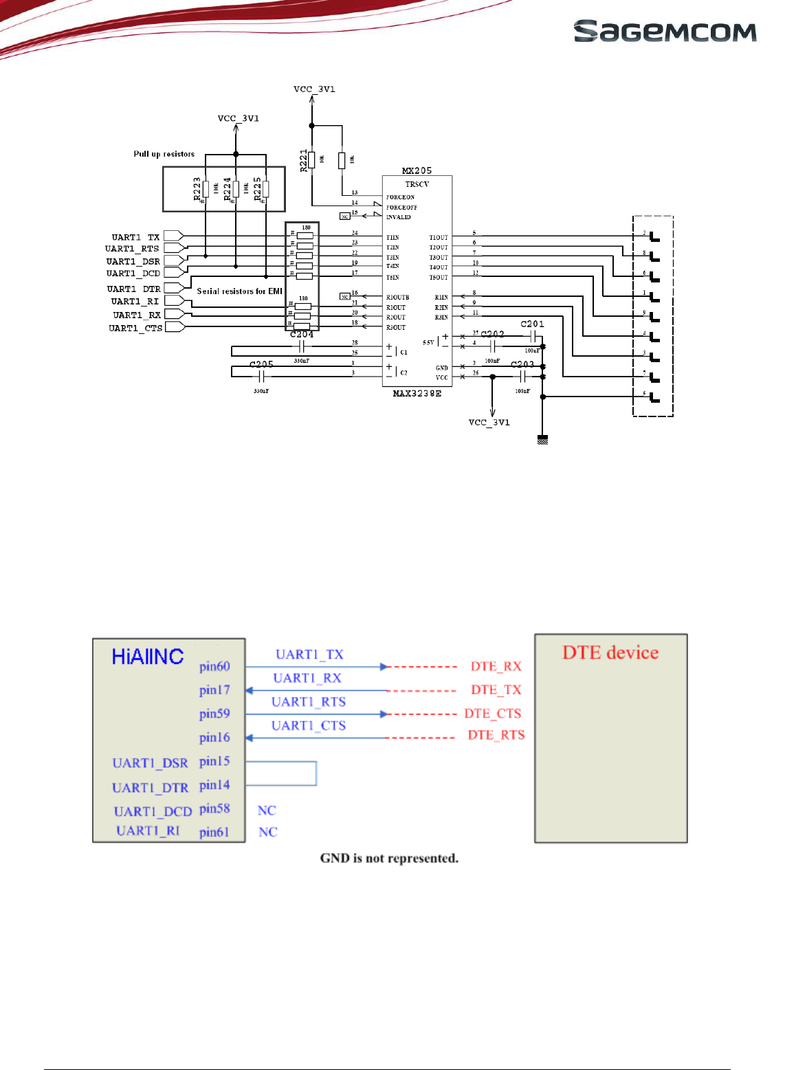
To create your own data cable (for software download purpose…etc…) refer to the following schematic as an
example with a MAX3238E:
• VCC_3V1 is an LDO output (VBAT to VCC_3V1) enabled by VGPIO from the module. Yet it can be any
voltage between 3V and 5V (see MAX3238E or MAX3237E specification).
• 180Ω are serial resistors aimed to limit the EMC and ESD propagation.
• Additional voltage level translator must be added to the design when GPIO of HiAll
NC
module was set to
1.8V mode.
page 25/51
HiAll
NC
User Manual 2012/06/28
Figure 18: Example of a connection to a data cable with a MAX3238E
3.5.3 Partial V24 (RX-TX-RTS-CTS) connection of HiAllNC to host
When using only UART1_RXD/ UART1_TXD/ UART1_RTS/ UART1_CTS instead of the complete V24 link, the
following schematic could be used.
Figure 19: Partial V24 connection (4 wires) of HiAll
NC
to host processor
As UART1_DTR is active (low electrical level) once HiAll
NC
is switched on, UART1_DSR is also active
(low electrical level), therefore the AT command AT+KSLEEP can switch between the two sleep modes.
UART1_DCD and UART1_RI can remain disconnected and floating when not in use. Otherwise use
100KΩ to pull up to power.
This configuration allows use of flow control UART1_RTS & UART1_CTS to avoid overflow error during data
transfer. Moreover UART1_RTS is used to indicate when the HiAll
NC
module is ready to receive an AT
page 26/51
HiAll
NC
User Manual 2012/06/28
command after power up sequence or wake up from sleep mode.
UART1_RI signal is a stand alone signal that can be used with any one of the following configuration.
Consult the AT command specification for more information about this signal and its use.
This configuration allows to use the flow control UART1_RTS & UART1_CTS to avoid any overflow error
during the data transfer, UART1_CTS is moreover used to signal when the HiAll
NC
is ready to receive an AT
command after a power up sequence or a wake up from sleep mode.
However this configuration does not allow signals such as:
• UART1_RI signal used when programmed to indicate an incoming voice or data call or SMS incoming
etc…
• UART1_DCD signal used to indicate DATA connections.
• UART1_DTR signal used to indicate module UART interface is ON.
• UART1_DSR signal is used to prevent HiAll
NC
from entering sleep mode or to switch between DATA
and AT commands or to hang up a call or to wake up the module etc….
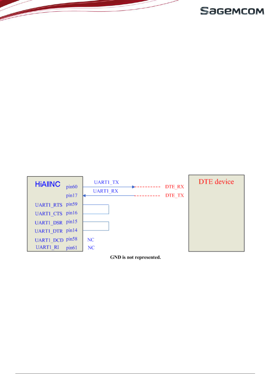
3.5.4 Partial V24 (RX-TX) – connection
HiAll
NC
- host
When using only UART1_RXD/ UART1_TXD instead of the complete V24 link, the following schematic could be
used.
Figure 20: Partial V24 connection (2 wires) of HiAll
NC
to host processor
As UART1_DTR is active (low electrical level) once HiAll
NC
is switched on, UART1_DSR is also active
(low electrical level), therefore the AT command “AT+KSLEEP” can switch between the two available sleep
modes.
As UART1_RTS is active (low electrical level) once HIALLNC is switched on, UART1_CTS is also active
(low electrical level), therefore the AT command “AT+ KSLEEP” can switch between the two available sleep
modes. The HiAll
NC
firmware allows activation of UART1_RTS during sleep state even when looped to the
UART1_CTS signal.
Note that this configuration does not allow the below signals:
• UART1_RI signal used when programmed to indicate an incoming voice or data call or incoming SMS
etc….
• UART1_DCD signal used to indicate GPRS connections.
• UART1_DTR signal used to indicate the module UART interface is ON.
• UART1_DSR signal used to prevent the HiAll
NC
module from entering sleep mode.
page 27/51
HiAll
NC
User Manual 2012/06/28
3.6
SPI
HiAllNC module manages a host SPI interface. This SPI interface is only dedicated for software traces.
SAGEMCOM strongly recommends leaving this interface externally accessible for SW traces (e.g.
access by test point pads)
In case of needs SAGEMCOM may request to connect a dedicated trace cable to the customer’s electronic
board.
If tests points have been foreseen, simply solder 5 wires to a small HE10 male connector using the following
schematic. This connector will be linked to the dedicated cable and used to log the software traces with a PC
software provided by SAGEMCOM.
Figure 21: SPI HE10 pin – TOP VIEW
3.7 GPIOS
Six GPIOs are available on HiAll
NC
. All GPIOs have optional internal pull-up resistors. Customer applications
can directly access them through appropriate AT commands such as:
• Output: pin is set to High or Low state
• Input: pin is read on request and customer application is responded to.
Different scenarios are possible to cover a maximum range of customer applications:
• Synchronous answer to AT command
• Asynchronous answer to AT command
Customer’s application prior to the read request has configured the GPIO to react to falling/rising edges. The
customer application is notified asynchronously by AT command answer when the configured trigger occurs.
By using other special AT commands, GPIOs can be used to, for example:
• to make an I/O toggling while the module is attached to the network
• to make an I/O toggling when a programmed temperature is reached
• as input to detect the presence of an antenna (with some external additional electronic circuit)
• as input to detect the SIM card presence …etc
GND (White) SPI_OUT (Red)
SPI_CLK (Yellow) SPI_IRQ (Green)
SPI_SEL (Brown)
SPI_IN (Black)
VCC_3.7V (Blue)
NC
Male connector located on the Customers' hardware
(HE10 male 8 pins)

page 28/51
HiAll
NC
User Manual 2012/06/28
3.8 ADCS
Two ADC input pads are available on HiAll
NC
module, which can be used to read the value of the voltage
applied. Following characteristics must be met to allow proper performances:
• The input signal voltage must be within 0V to 3V
• The input impedance of the pad is 150KΩ
• The input capacitance typically is 10pF.
• 10 bits resolution
• Maximum sampling frequency is 200KHz.
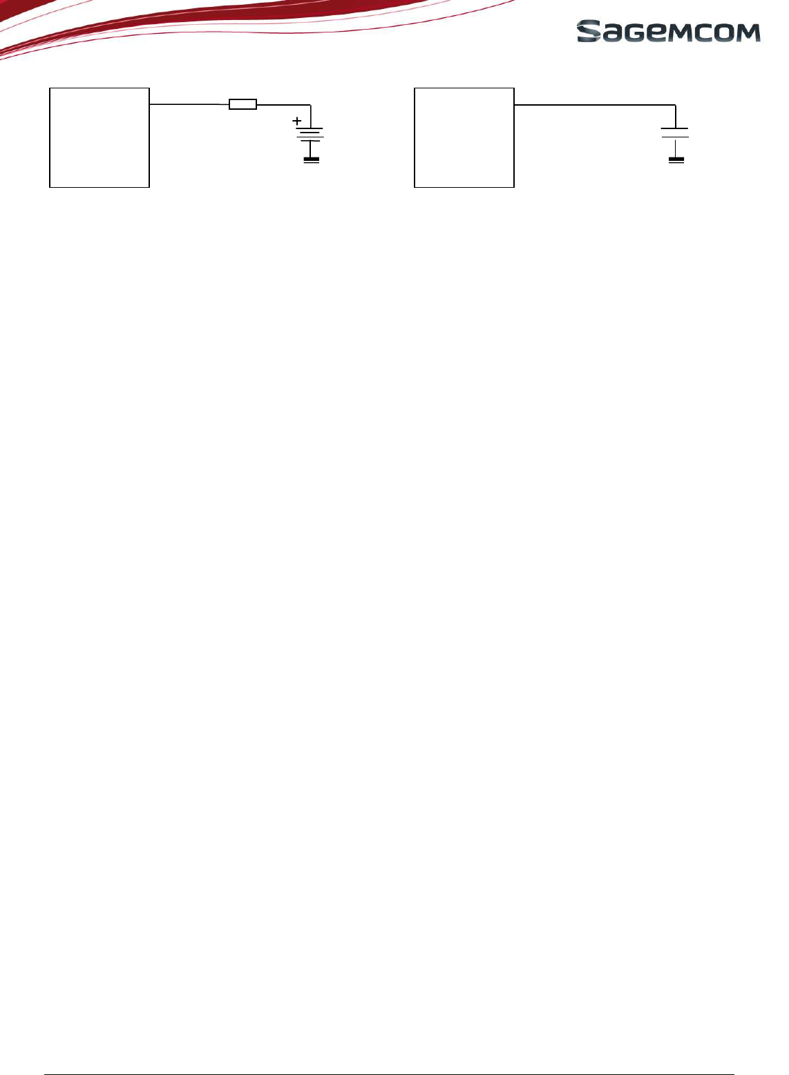
3.9 BACKUP BATTERY
3.9.1 Backup battery function features
A backup battery can be connected to the module in order to supply internal RTC (Real Time Clock) when the
main power supply is disconnected.
With external backup battery:
• If VBAT < 3V, internal RTC is supplied by VBACKUP.
• If VBAT ≥3V, internal RTC is supplied by VBAT.
Without backup battery
• If VBAT ≥ 1.5V, internal RTC is supplied by VBAT.
• If VBAT < 1.5V, internal RTC is not supplied.
VBACKUP input of the module has to be connected to a 10µF capacitor (between VBACKUP and GND).
3.9.2 Current consumption on the backup battery
When the power supply is removed, the internal RTC will be supplied by backup battery.
To calculate the backup battery capacity, consider that current consumption for RTC on the backup
battery is up to 1000µA in worst case conditions.
Signals Min current Max current
VBACKUP 1000µA
3.9.3 Internal
HiAll
NC
charging function
HiAll
NC
has a charging function that does not require any additional external power supply (power supply for the
charging is provided by the HiAll
NC
).
Charge of the back-up battery occurs only when main power supply VBAT is provided.
The recommended schematic is given hereafter:
page 29/51
HiAll
NC
User Manual 2012/06/28
Figure 22: internal charging of backup battery or 10uF capacitor
The value of resistor R depends on the charging current value of the backup battery manufacturer.
3.9.4 Capacitor backup battery technology
SAGEMCOM strongly recommends using Supercap technology.
These kinds of backup battery have not the drawbacks of the Lithium Ion rechargeable battery.
As there are only capacitors:
• The maximum discharge current is generally bigger,
• There is no problem of over-discharge: the capacitor is able to recover its full charge even if its voltage
has previously fallen to 0V.
• There is no need to regulate the charging current.
Moreover, this kind of battery is available in the same kind of package than the Lithium Ion cell and fully
compatible on a mechanical point of view. The only disadvantage is that the capacity of this kind of battery is
significantly smaller than Manganese Silicon Lithium Ion battery. But for this kind of use (supply internal RTC
when the main battery is removed), the capacity is generally enough.
VBACKUP
HiAll
NC
10µF capacitor
VBACKUP
HiAll
NC
R
Backup battery
page 30/51
HiAll
NC
User Manual 2012/06/28
4. UNUSED PINS POLICY
The table below defines the connection requirement of unused pins, as well as mandatory connections.
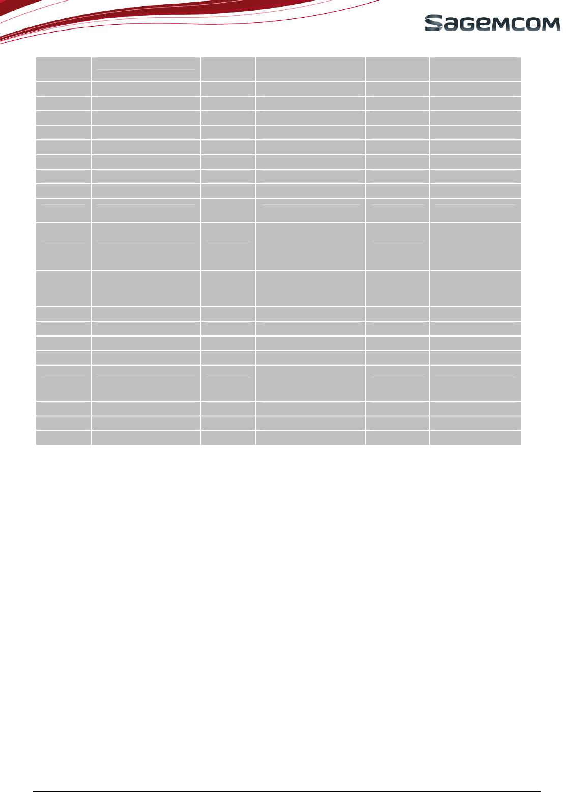
LGA Pin Signal Name Connection when not used / Mandatory
connection
1-3 GND 0V
4 RF_GSM GSM Antenna
5-8 GND 0V
9 RESERVED
(3G compatibility) Left Open
10 GND 0V
11 RF_GPS GPS Antenna
12 GND 0V
13 PPS Left Open
14 UART1_DTR Loop to UART1_DSR
15 UART1_DSR Loop to UART1_DTR
16 UART1_CTS Loop to UART1_RTS
17 UART1_RX UART1_RX
18 UART0_TX Left Open
19 UART0_RTS Loop to UART0_CTS
20 RESERVED
(3G compatibility) Left Open
21 PCM_CLK Left Open
22 PCM_SYNC Left Open
23 HSET_N Left Open
24 HSET_P Left Open
25 MIC_P Left Open
26 MIC_N Left Open
27 RESET Left Open
28 VBACKUP C=10µF
29 VBAT VBAT
30 ADC1 Left Open
31 ADC0 Left Open
32 POK_IN POWER ON
33 SIM_VCC SIM VCC (external SIM)
Left Open (if embedded SIM, and no plan to
support external SIM)
34 SIM_DATA SIM DATA (external SIM)
Left Open (if embedded SIM, and no plan to
support external SIM)
35 SIM_CLK SIM CLK (external SIM)
Left Open (if embedded SIM, and no plan to
support external SIM)
36 GPIO1 Left Open
37 SPI_IRQ Left Open
38 RESERVED
(futur use) Left Open
39 GPS_EXT_LNA_EN Left Open
40 GPIO2 Left Open
page 31/51
HiAll
NC
User Manual 2012/06/28
41 GPIO3 Left Open
42 TRST Left Open
43 VBAT_PA VBAT_PA
44 VBAT_PA VBAT_PA
45-56 GND 0V
57 VBAT VBAT
58 UART1_DCD Left Open
59 UART1_RTS Loop to UART1_CTS
60 UART1_TX UART1_TX
61 UART1_RI Left Open
62 UART0_RX Left Open
63 UART0_CTS Loop to UART0_RTS
64 RESERVED
(3G compatibility) Left Open
65 PCM_OUT Left Open
66 PCM_IN Left Open
67 RESERVED
(3G compatibility) Left Open
68 RESERVED
(3G compatibility) Left Open
69 RESERVED
(3G compatibility) Left Open
70 RESERVED
(3G compatibility) Left Open
71 VGPIO Left Open
72 SPI_IN Left Open
73 SPI_OUT Left Open
74 SPI_SEL Left Open
75 SPI_CLK Left Open
76 TMS Left Open
77 TDI Left Open
78 TDO Left Open
79 SIM_RST SIM RST (external SIM)
Left Open (if embedded SIM, and no plan to
support external SIM)
80 JTAG_TEST Left Open
81 RESERVED
(Factory use) Left Open
82 TCK Left Open
83 GPIO4 Left Open
84 GPIO5 Left Open
85 GPIO6 Left Open
86 VIO_SEL Left Open
87 2G_RF_IND Left Open
88 RTCK Left Open
89-116 GND 0V
page 32/51
HiAll
NC
User Manual 2012/06/28
5. SCALABILITY WITH HILO
NC
-3GPS
The table below defines the pin & supply voltage matching between HiAll
NC
and HiLo
NC
-3GPS .
Pad
number HiAll
NC
Pad name
Supply
voltage
domain
Note 1
Hilo
NC
-3GPS
Pad name
Supply
voltage
domain Note
1-3 GND 0V GND 0V
4 RF_GSM RF
5-8 GND 0V GND 0V
9 RESERVED
(Not connected
internally) AUX AUX signal can
be left connected
to HiAll
NC
pad
10 GND 0V GND 0V
11 RF_GPS GPS
12 GND 0V GND 0V
13 PPS 2.8V RESERVED
(Not connected
internally)
PPS signal can
be left connected
to Hilo
NC
-3GPS
pad
14 UART1_DTR 2.8V UART_DTR 1.8V
15 UART1_DSR 2.8V UART_DSR 1.8V
16 UART1_CTS 2.85V UART_CTS 1.8V
17 UART1_RX 2.85V UART_RX 1.8V
18 UART0_TX 2.85V SDIO_CMD 2.85V
19 UART0_RTS 2.8V SDIO_DATA2 2.85V
20 RESERVED
(Not connected
internally) - SDIO_DATA0 2.85V
21 PCM_CLK 2.85V PCM_CLK 1.8V
22 PCM_SYNC 2.85V PCM_SYNC 1.8V
23 HSET_N 3.7V RESERVED
(Not connected
internally)
HSET_N signal
can be left
connected to
Hilo
NC
-3GPS pad
24 HSET_P 3.7V
RESERVED
(Not connected
internally)
HSET_P signal
can be left
connected to
Hilo
NC
-3GPS pad
25 MIC_P 2.85V
RESERVED
(Not connected
internally)
MICP_P signal
can be left
connected to
Hilo
NC
-3GPS pad
26 MIC_N 2.85V
RESERVED
(Not connected
internally)
MIC_N signal can
be left connected
to Hilo
NC
-3GPS
pad
27 RESET 2.8V RESET 1.8V
28 VBACKUP 3V VBACKUP 3V
29 VBAT 3.7V VBAT 3.7V
30 ADC1 2.85V ADC 2.1V
31 ADC0 2.85V RESERVED
(Not connected
internally)
ADC0 signal can
be left connected
to Hilo
NC
-3GPS
pad
page 33/51
HiAll
NC
User Manual 2012/06/28
32 POK_IN 3V PWON 1.8V
33 SIM_VCC 1.8V/2.9
V SIM_VCC 1.8V/2.9V
34 SIM_DATA 1.8V/2.9
V SIM_DATA 1.8V/2.9V
35 SIM_CLK 1.8V/2.9
V SIM_CLK 1.8V/2.9V
36 GPIO1 2.8V
RESERVED
(Not connected
internally)
GPIO1 signal can
be left connected
to Hilo
NC
-3GPS
pad
37 SPI_IRQ 2.8V
RESERVED
(Not connected
internally)
SPI_IRQ signal
can be left
connected to
Hilo
NC
-3GPS pad
38 RESERVED
(Not connected
internally) RESERVED
(Not connected
internally)
39 GPS_EXT_LNA_EN 2.8V GPS_LNA_EN
GPIO1 1.8V
40 GPIO2
2.8V SIM_DET
GPIO2 1.8V
41 GPIO3 2.8V GPIO3 1.8V
42 TRST 2.8V TRST 1.8V
43 VBAT_PA 3.7V VBAT 3.7V
44 VBAT_PA 3.7V VBAT 3.7V
45-56 GND 0V GND 0V
57 VBAT 3.7V RESERVED
(Not connected
internally) 3.7V
HiAll
NC
mandatory
connection
VBAT can be left
connected to
Hilo
NC
-3GPS pad
58 UART1_DCD 2.8V UART_DCD 1.8V
59 UART1_RTS 2.85V UART_RTS 1.8V
60 UART1_TX 2.85V UART_TXD 1.8V
61 UART1_RI 2.8V UART_RI 1.8V
62 UART0_RX 2.85V SDIO_CLK 2.85V
63 UART0_CTS 2.8V SDIO_DATA3 2.85V
64 RESERVED - SDIO_DATA1 2.85 V
65 PCM_OUT 2.85V PCM_OUT 1.8V
66 PCM_IN 2.85V PCM_IN 1.8V
67 RESERVED
(Not connected
internally) - USB_DN 3.075V
USB_DP can be
left connected to
HiAll
NC
pad if tied
to static signal
68 RESERVED
(Not connected
internally) - USB_DP 3.075V
USB_DP can be
left connected to
HiAll
NC
pad if tied
to static signal
69 RESERVED
(Not connected
internally) - USB_VBUS 5V
USB_VBUS can
be left connected
to HiAll
NC
pad if
tied to static
signal
70 RESERVED
(Not connected - PWM 2.85V PWM can be left
connected to
page 34/51
HiAll
NC
User Manual 2012/06/28
internally) HiAll
NC
pad if tied
to static signal
71 VGPIO 2.8V VGPIO 2.85V
72 SPI_IN 2.8V SPI_IN 1.8V
73 SPI_OUT 2.8V SPI_OUT 1.8V
74 SPI_SEL 2.8V SPI_SEL 1.8V
75 SPI_CLK 2.8V SPI_CLK 1.8V
76 TMS 2.8V TMS 1.8V
77 TDI 2.8V TDI 1.8V
78 TDO 2.8V TDO 1.8V
79 SIM_RST 1.8V/2.9
V SIM_RST 1.8V/2.9V
80 JTAG_TEST 2.8V
RESERVED
(Not connected
internally)
JTAG_TEST
signal can be left
connected to
Hilo
NC
-3GPS
81 RESERVED
(Factory use, left
open) RESERVED
(Not connected
internally) Do not connect
82 TCK 2.8V TCK 1.8V
83 GPIO4 2.8V GPIO4 1.8V
84 GPIO5 2.8V GPIO5 1.8V
85 GPIO6 2.8V GPIO6 1.8V
86 VIO_SEL RESERVED
(Not connected
internally)
87 2G_RF_IND 2.85V 2G_RF_IND 1.8V
88 RTCK 2.8V RTCK 1.8V
89-116 GND 0V GND 0V
Note 1: VIO_SEL (pad86) left unconnected
.

page 35/51
HiAll
NC
User Manual 2012/06/28
6. POWER MANAGEMENT
VBAT Input voltage shall be in the range 3.3V to 4.5V.
6.1 POWER MODES
Depending on the status of the HiAll
NC
, different power consumption modes can be identified.
Communication mode (with or without GPS running)
All systems on HiAll
NC
are active. In this mode, the module is registered to the network and a voice/data call is
actively transmitting data.
Idle mode (with or without GPS running)
In this mode, the module is registered to the network but it is idle/ paging only. No voice/ data call connection is
established. AT commands can be send and GPS can run.
Sleep mode (without GPS running)
In this mode, the module is registered to the network but it is idle/ paging only. No voice/data call connection is
established. AT commands can not be send.
Flight mode (with or without GPS running)
The processor is still active but the radio section is powered down. This mode can be controlled by sending an
AT command to the module.
6.2 MODULE POWER-UP
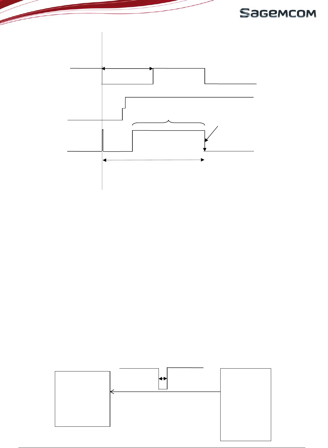
6.2.1 Power-up with POK_IN signal
To start the module, first power up VBAT, which must be in the range 3.3V ~ 4.5V, and must be able to supply
1.8A during TX bursts.
POK_IN is a low level active signal internally pulled up to a dedicated power domain of 3V.
As POK_IN is internally pulled up, a simple open collector or open drain transistor must be used for ignition.
Warning: The POK_IN will become low after module is ready. It can not be directly driven by a GPIO
signal.
To start the module, a low level pulse must be applied on POK_IN for 2000ms.
RESET must not be Low during that period of time
After a few seconds, the UART1_RTS enters active state and the module is ready to receive AT commands.
VGPIO is a supply output from the module that can be used to check if the module is active.
• When VGPIO = 0V the module is OFF.
• When VGPIO = 2.8V the module is ON. (It can be in Idle, communication or sleep modes)
page 36/51
HiAll
NC
User Manual 2012/06/28
Figure 24: Power ON sequence
6.2.2 IO DC Presence before Power on
When VBAT is available but the module has not yet powered up, the following I/O's raise their output.
POK_IN raise to 3V
VBACKUP raise to 3V
HSET_N raise to 1.4V
HSET_P raise to 1.4V
6.2.3 MODULE RESET
To reset the module, a low level pulse must be sent on RESET pin during 10 ms. This action will immediately
restart the HiAll
NC
module. It is therefore useless to perform a new ignition sequence (POK_IN) after.
SAGEMCOM recommends using this feature in case of emergency, freeze of module or abnormal longer
time to respond to AT Commands, this signal is the only way to get the control back over the HiAll
NC
module.
RESET is a low level active signal internally pulled up to a dedicated power domain.
As RESET is internally pulled up, a simple open collector or open drain transistor can be used to control it.
Figure 23: Reset command of the HiAll
NC
by an external GPIO
HiAll
NC
Module
DCE
HOST
DTE
RESET
10ms
2.4V min
0.4V max
GPIO
2.8V
POK_IN
VGPIO
spike
Software Loading
Module is ready
to receive AT
commands
Module is
OFF
Module is
ON
2000ms
CTS
Typ 5 seconds
Max 7 seconds

page 37/51
HiAll
NC
User Manual 2012/06/28
The RESET signal will reset the registers of the CPU and reset the RAM memory as well.
As RESET is referenced to VGPIO domain (internally to the module) it is impossible to make a reset
before the module starts or try to use the RESET as a way to start the module.
An other solution more costly would be to use MOS transistor to switch off the power supply and restart the
power up procedure using the POK_IN input line
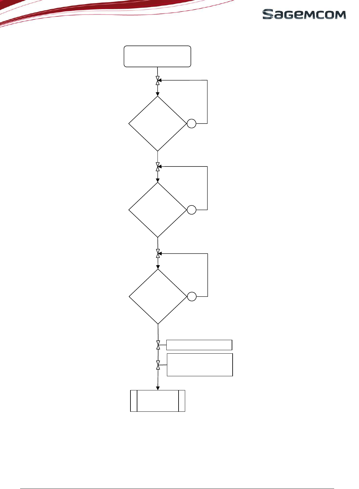
6.3 POWER ON AND SLEEP DIAGRAMS
Those 2 diagrams show the behaviours of the module and the DTE during the power on and then in the sleep
modes.
page 38/51
HiAll
NC
User Manual 2012/06/28
Figure 24: Diagram for the power on
DTE is in idle mode
VGPIO rise to 2.8V
U.A.R.T.
closed ?
VBAT≥3.3
Volts min
stable?
POK_IN
LOW for 2s
AND Reset
High?
CTS is Low and /or
KSUP
notified if KSREP
activated
Module is ready
to receive and
send AT
page 39/51
HiAll
NC
User Manual 2012/06/28
Figure 25: Diagram for the sleep mode
Ksleep = 1 OR
( Ksleep = 0
AND
DTR = High)
Module is ready to
receive and send AT
VGPIO remains at 2.8V
RI signal
connected
and
programmed?
Module is in
sleep m
Sleep mode request
Delay to enter the sleep
mode
CTS is High
The wakes up
periods are set by
the network DRX
or the OS
DTE could
also
be in sleep
mode
Wake up incoming event such as:
• Network event.
• Alarm interruption.
• DTR interruption.
• RTS interruption.
RI wakes the DTE
DTE is in idle mode
page 40/51
HiAll
NC
User Manual 2012/06/28
6.4 MODULE POWER OFF
AT command “AT*PSCPOF” allows for correct power-off of the HiAll
NC
module.
In case of necessary the module can be powered off by controlling the power supply. This can be used for
example when the system freezes and no reset line is connected to the HiAll
NC
. In this case the only way to get
the control back over the module is to switch off the power line. If the system is on a battery, it is wise to have a
control of the power supply by a GPIO with for example the following schematic.
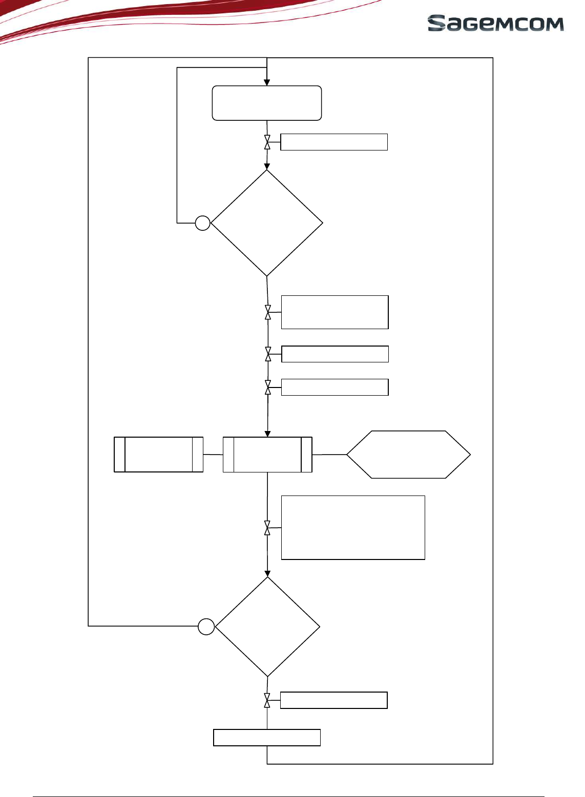
Figure 26: Power supply command by a GPIO
This kind of schematic could also be used to save few micro amperes in case of need. As the module has
a drain current of up to 56µA, this kind of function could lower it to the current through R4.
These, are the behaviours of the VGPIO and the CTS signal during the power off sequence.
Figure 27: Power OFF sequence for POK_IN, VGPIO and CTS
POK_IN is low
VGPIO
Module is ON Module is OFF
Typ 2 seconds
AT*PSCPOF
CTS
POK_IN is high

page 41/51
HiAll
NC
User Manual 2012/06/28
6.5 MODULE SLEEP MODE
The AT command “AT+KSLEEP” allows to configure the sleep mode.
When AT+KSLEEP=1 is configured:
• The HiAll
NC
module decides by itself when it enters in sleep mode (no more task running).
• “0x00” character on serial link wakes up the HiAll
NC
module.
When AT+KSLEEP=0 is configured:
• When UART1_DTR is deactivated (high electrical level), the HiAll
NC
module enters in sleep mode after
a while.
• On UART1_DTR activation (low electrical level), the HiAll
NC
module wakes up.
When AT+KSLEEP=2 is configured:
• The HiAll
NC
module does not enter in sleep mode.
In sleep mode the module reduces its power consumption and remains waiting for the wake up signals either
from the network (i.e. Read paging block depending on the DRX value of the network) or the operating system
(i.e. timers wake up timers activated) or the host controller (i.e. character on serial link or UART1_DTR signal).

page 42/51
HiAll
NC
User Manual 2012/06/28
7. ESD & EMC RECOMMENDATIONS
7.1
HiAll
NC
MODULE
HiAll
NC
module alone can hold up to 2KV on each of the 116 pads including the RF pad.
7.2 Module handling
HiAll
NC
modules are designed and packaged in tape-and-real for factories SMT process.
HiAll
NC
modules contain electronic circuits sensitive to human hand's electrostatic electricity.
Handling without ESD protection could result in permanent damages or even destruction of the module.
7.3 Customer’s product with
HiAll
NC
If customer’s design must stand more than 2kV on electrostatic discharge, following recommendation must be
followed.
7.4 Analysis
ESD current can penetrate inside the device via the typical following components:
• SIM connector
• Microphone
• Speaker
• Battery / data connector
• All pieces with conductive paint.
In order to avoid ESD issues, efforts shall be done to decrease the level of ESD current on electronic
components located inside the device
7.5 Recommendations to avoid ESD issues
Insure good ground connections of the HiAll
NC
module to the customer’s board.
Flex (if any) shall be shielded and FPC connectors shall be correctly grounded at each extremity.
Put capacitor on battery 100nF or varistor or ESD diode in parallel on battery and charger wires (if any)
and on all power wires connected to the module.
Uncouple microphone and speaker by putting capacitor or varistor in parallel of each wire of these
devices.
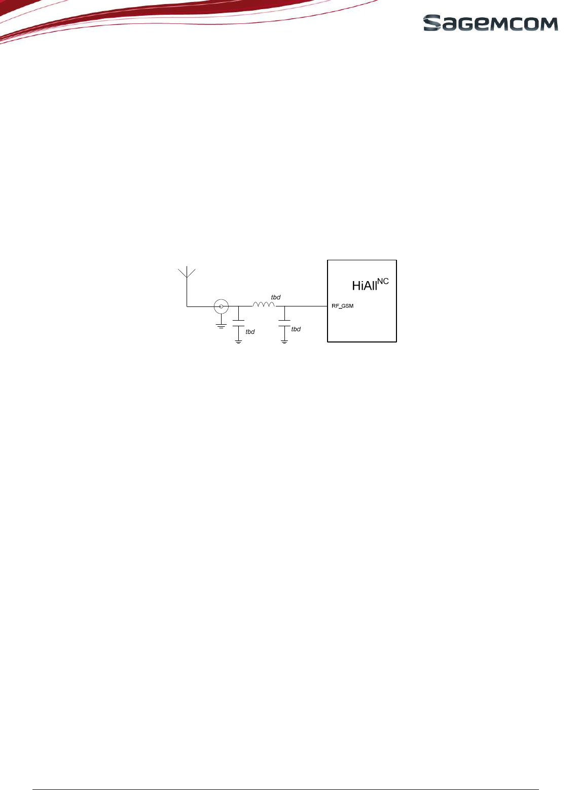
page 43/51
HiAll
NC
User Manual 2012/06/28
8. RADIO INTEGRATION
Radio engineering skills are mandatory to get accurate radio performance on customer’s product
8.1
GSM antenna connection
RF lines shall match 50 ohms impedance
In order to achieve optimum sensitivity and output power in radiated mode, it is strongly recommended to
implement a matching circuit, as shown on schematic below
Figure 28: GSM antenna connection schematic
More information about GSM radio design can be found in [3].
8.2 GNSS
antenna connection
8.2.1 Reference schematics
HiAll
NC
module supports both passive and active antenna.
HiAll
NC
embeds a high performance SAW filter. No external filtering is required.
Typical schematic for passive antenna is similar to GSM antenna schematic above.
If active antenna use, HiAll
NC
module can be configure to output a GPS_LNA_EN signal, allowing
disabling the external LDO when GNSS receiver is in stand-by or shut-down mode.
Enabling GPS_LNA_EN is performed through AT+GNSSRUN command
If active antenna connection, a power supply shall be connected to the GNSS feed point, according to
schematic example below:
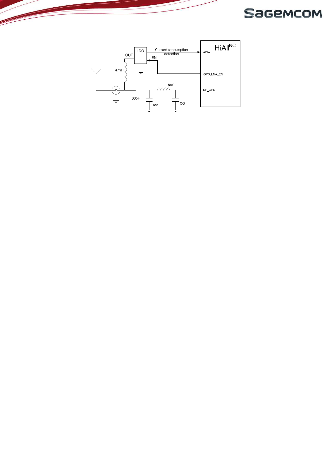
page 44/51
HiAll
NC
User Manual 2012/06/28
Figure 29: GNSS active antenna connection schematic
8.2.2 Antenna detection
For passive antenna, the command AT+KGNSSAD can be used to perform antenna detection.
For active antenna, a GPIO can be used to detect the antenna power consumption. The customer needs to fit
the current sense circuitry on its own board and match the detection level to the VGPIO level.
8.3 RADIO LAYOUT DESIGN
Radio layout guidelines are defined in document [3]

page 45/51
HiAll
NC
User Manual 2012/06/28
9. AUDIO INTEGRATION
FTA audio mandatory tests only deal with handset mode so a particular care must be brought to the design of
audio (mechanical integration, gasket, electronic) in this mode.
The audio related standard are 3GPP TS 26.131 & 3GPP TS 26.132.
Note that acoustic competences are mandatory to get accurate audio performance on customer’s product.
9.1 MECHANICAL INTEGRATION AND ACOUSTICS
Particular care to Handset Mode:
To achieve a more ideal audio output design (speaker part):
The speaker must be completely sealed on front side.
The front aperture must be compliant with the speaker supplier’s specifications
The back volume must be completely sealed.
The sealed back volume must be compliant with the speaker supplier’s specifications
Pay attention to the design of the speaker gasket (elastomer).
Make sure to leave sufficient space for the artificial ear gasket.
To achieve a more ideal audio input design (microphone part):
Pay attention to the design of the microphone (elastomer).
All receivers must be completely sealed on front side.
Microphone sensitivity depends on the shape of the device but should be in the range of –40 ±3 dBV/Pa.
Recommend to use the pre-amplified microphone. If needed, use a pre-amplification stage.
As audio input and output are strongly linked:
Place the microphone and the speaker as far away as possible from one another.
9.2 ELECTRONICS AND LAYOUT
Avoid Distortion & Burst noise
Audio signals must be symmetric (same components on each path).
Differential signals must be routed in parallel.
Audio layer must be surrounded by 2 ground layers.
The link from one component to the ground must be as short as possible.

page 46/51
HiAll
NC
User Manual 2012/06/28
Separate the PCBs for the microphone and the speaker if possible.
Reduce the number of electronic components as much as possible (to avoid loss of quality and greater
dispersion).
Audio tracks must be larger than 0.5 mm.

page 47/51
HiAll
NC
User Manual 2012/06/28
10. LAYOUT RECOMMENDATIONS ON CUSTOMER BOARD
10.1 GENERAL RECOMMENDATIONS ON LAYOUT
There are many different types of signals in the module which may be interfered each other. Particularly, Audio
signals are very sensitive to external signals such as VBAT... Therefore it is very important to follow some rules
to avoid signal disruption or abnormal behaviour.
Magnetic fields generated by VBAT tracks may cause speaker interference and burst noise. In this case,
modify layout of the VBAT tracks to reduce the phenomenon.
10.1.1 Ground
Ensure the ground plane is as complete as possible
Grounding of components should be connected to the ground layer through a number of irregularly
distributed vias.
Top and bottom layer should set aside as much space for the ground plane as possible. Flood remaining
empty surfaces of the layout of those two layers with a ground plane connected to the main ground through as
many vias as possible.
Proper grounding is crucial to end-product performance. At least one layer must be a dedicated ground
plane. This ground plane is the common point referenced by all end-product circuits.
In addition to the dedicated ground plane layer, unused space on all PCB layers should be filled with
grounding to provide the most robust grounding possible from layer to layer.
Bypass capacitors should be connected directly to their surface layer ground fill. Multiple vias should
connect each capacitor directly to the main ground plane, with one via in the capacitor’s pad plus several vias
within the surface layer ground fill area.
Digital ground should connect directly to the main ground plane. In addition, each layer between layer 1
and the main ground should include ground fills directly below the center grid area’s digital pins, with each stack
of vias connecting to each ground fill area. The large mass of copper tied together using this technique provides
optimal electrical grounding and thermal conductivity.
The analog/RF ground pins are connected to each other, but isolated from the digital ground (until main
ground). Like the digital pins, the analog/RF pins should connect directly to the main ground plane. In addition,
each layer between layer 1 and the main ground should include ground fills directly below the outer layer’s
analog/RF pins, with each stack of vias connecting to each ground fill area. The large mass of copper tied
together using this technique provides optimal electrical grounding and thermal conductivity.
10.1.2 Power supplies
A layer for power supply signals (VBAT, VGPIO,SIM_VCC_VCC) is recommended.
Looping of power signal layouts must be avoided in device design.
Ensure suitable power supply (VBAT, VGPIO,SIM_VCC) track width and thickness.
page 48/51
HiAll
NC
User Manual 2012/06/28
10.1.3 Clocks
Clock signals must be shielded between two grounds layer and bordered with ground vias.
10.1.4 Data bus and other signals
Data bus must be routed on the same layer with equivalent track length and avoiding long parallel routing.
Lines crossings shall be perpendicular
Suitable signals track width, thickness for other signals.
Data bus must be protected by upper and lower ground plans
10.1.5 Radio
Provide a 50 Ohm micro strip line for antenna connection
For RF matching components do not locate matching inductors too close to shield walls (this may cause
electromagnetic coupling and inductor de-Q).
10.1.6 Audio
Differential signals have to be routed together, parallel (for example HSET_OUT_P/HSET_OUT_N,
MIC_P/MIC_N).
Audio signals have to be isolated, by pair, from all the other signals (ground all around each pair).
Cancel any loops between VBAT and GND next to the speaker to avoid the TDMA burst noise in the
speaker during a communication.
The single-end audio signal should be adopted the same rules as differential signals.
Figure 30: Layout of audio differential signals on a layer n
Figure 31: Adjacent layers of audio differential signals
Layer n-1
Layer n
Layer n+1
GND
HSET_OUT_P
GND
GND
HSET_OUT_P
GND
HSET_OUT_N
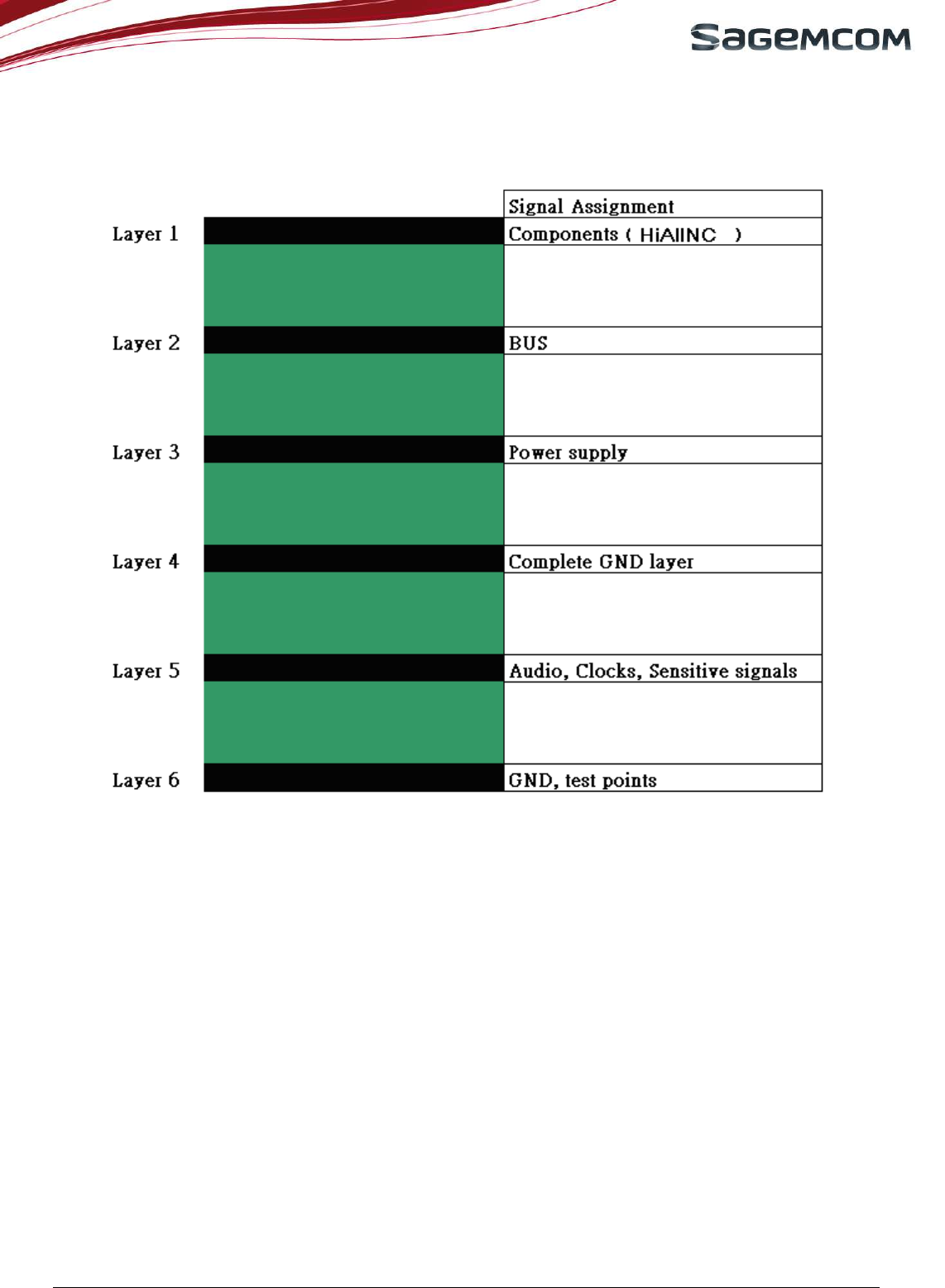
page 49/51
HiAll
NC
User Manual 2012/06/28
10.2 EXAMPLE OF LAYOUT FOR CUSTOMER’S BOARD
The following figure is an example of layer allocation for a 6 layers circuit (for reference purpose only):
Depending on the customer’s design, the layout could also be 4 layers.
Figure 32: 6 layers PCB stack-up
11. LABEL
The HiAll
NC
module is labelled with its own FCC ID (VW3HIALLNC) on the shield side. When the module is
installed in customer’s product, the FCC ID label on the module will not be visible. To avoid this case, an
exterior label must be stuck on the surface of customer’s product signally to indicate the FCC ID of the enclosed
module. This label can use wording such as the following: “Contains Transmitter module FCC ID:
VW3HIALLNC” or “Contains FCC ID: VW3HIALLNC ”.
12. FCC LEGAL INFORMATION
12.1 FCC REGULATIONS
This device complies with part 15 of the FCC Rules. Operation is subject to the following two conditions: (1) This
device may not cause harmful interference, and (2) this device must accept any interference received, including
interference that may cause undesired operation.

page 50/51
HiAll
NC
User Manual 2012/06/28
This device has been tested and found to comply with the limits for a Class B digital device, pursuant to Part 15
of the FCC Rules. These limits are designed to provide reasonable protection against harmful interference in a
residential installation. This equipment generates uses and can radiate radio frequency energy and, if not
installed and used in accordance with the instructions, may cause harmful interference to radio communications.
However, there is no guarantee that interference will not occur in a particular installation If this equipment does
cause harmful interference to radio or television reception, which can be determined by turning the equipment
off and on, the user is encouraged to try to correct the interference by one or more of the following measures:
Reorient or relocate the receiving antenna
Increase the separation between the equipment and receiver.
Connect the equipment into an outlet on a circuit different from that to which the receiver is connected.
Consult the dealer or an experienced radio/TV technician for help.
Changes or modifications not expressly approved by the party responsible for compliance could void the user’s
authority to operate the equipment.
12.2 RF EXPOSURE INFORMATION
This Modular Approval is limited to OEM installation for mobile and fixed applications only. The antenna
installation and operating configurations of this transmitter, including any applicable source-based time-
averaging duty factor, antenna gain and cable loss must satisfy MPE categorical Exclusion Requirements of
§2.1091.
The antenna(s) used for this transmitter must be installed to provide a separation distance of at least 20 cm
from all persons, must not be collocated or operating in conjunction with any other antenna or transmitter,
except in accordance with FCC multi-transmitter product procedures.
The end user has no manual instructions to remove or install the device and a separate approval is required for
all other operating configurations, including portable configurations with respect to 2.1093 and different antenna
configurations.
According to the MPE RF explore report, maximum antenna gain allowed for use with this device is 7.3dBi for
GSM850 and 2.9dBi for PCS1900.
When the module is installed in the host device, the FCC ID label must be visible through a window on the final
device or it must be visible when an access panel, door or cover is easily re-moved. If not, a second label must
be placed on the outside of the final device that contains the following text: ―Contains FCC ID: VW3HIALLNC.
12.3 IC REGULATIONS
IMPORTANT NOTE
IC Radiation Exposure Statement:
This equipment complies with IC RSS-102 radiation exposure limits set forth for an uncontrolled environment.
This equipment should be installed and operated with minimum distance 20cm between the radiator & your
body.
This device and its antenna(s) must not be co-located or operating in conjunction with any other antenna or
transmitter.
This Class B digital apparatus complies with Canadian ICES-003.
Cet appareil numérique de la classe B est conforme à la norme NMB-003 du Canada.
Under Industry Canada regulations, this radio transmitter may only operate using an antenna of a type and
maximum (or lesser) gain approved for the transmitter by Industry Canada. To reduce potential radio

page 51/51
HiAll
NC
User Manual 2012/06/28
interference to other users, the antenna type and its gain should be so chosen that the equivalent isotropically
radiated power (e.i.r.p) is not more than necessary for successful communication.
Conformément à la réglementation d'Industrie Canada, le présent émetteur radio peut fonctionner avec une
antenne d'un type et d'un gain maximal (ou inférieur) approuvé pour l'émetteur par Industrie Canada. Dans le
but de réduire les.risques de brouillage radioélectrique à l'intention des autres utilisateurs, il faut choisir le type
d'antenne et son gain de sorte que la puissance isotrope rayonnée équivalente (p.i.r.e.) ne dépasse pas
l'intensité nécessaire à l'établissement d'une communication satisfaisante.
Labeling Requirements for the Host Device (from Section 3.2.1, RSS-Gen, Issue 3, December 2010):The host
device shall be properly labeled to identify the module within the host device.The Industry Canada certification
label of a module shall be clearly visible at all times when installed in the host device, otherwise the host device
must be labeled to display the Industry Canada certification number of the module, preceded by the words ―
Contains transmitter module‖, or the word ―Contains‖, or similar wording expressing the same meaning, as
follows: Contains transmitter module IC: 9140A-HIALLNC.
This device complies with Industry Canada license-exempt RSS standard(s). Operation is subject to the
following two conditions: (1) this device may not cause interference, and (2) this device must accept any
interference, including interference that may cause undesired operation of the device.Le présent appareil est
conforme aux CNR d'Industrie Canada applicables aux appareils radio exempts de licence.
L'exploitation est autorisée aux deux conditions suivantes: (1) l'appareil ne doit pas produire de brouillage, et (2)
l'utilisateur de l'appareil doit accepter tout brouillage radioélectrique subi, même si le brouillage est susceptible
d'en.compromettre le fonctionnement.
This radio transmitter (identify the device by certification number, or model number if Category II) has been
approved by Industry Canada to operate with the antenna types listed below with the maximum permissible gain
and required antenna impedance for each antenna type indicated. Antenna types not included in this list, having
a gain greater than the maximum gain indicated for that type, are strictly prohibited for use with this device.
Conformément à la réglementation d'Industrie Canada, le présent émetteur radio peut fonctionner avec une
antenne d'un type et d'un gain maximal (ou inférieur) approuvé pour l'émetteur par Industrie Canada. Dans le
but de réduire les risques de brouillage radioélectrique à l'intention des autres utilisateurs, il faut choisir le type
d'antenne et son gain de sorte que la puissance isotrope rayonnée équivalente (p.i.r.e.) ne dépasse pas
l'intensité nécessaire à l'établissement d'une communication satisfaisante.